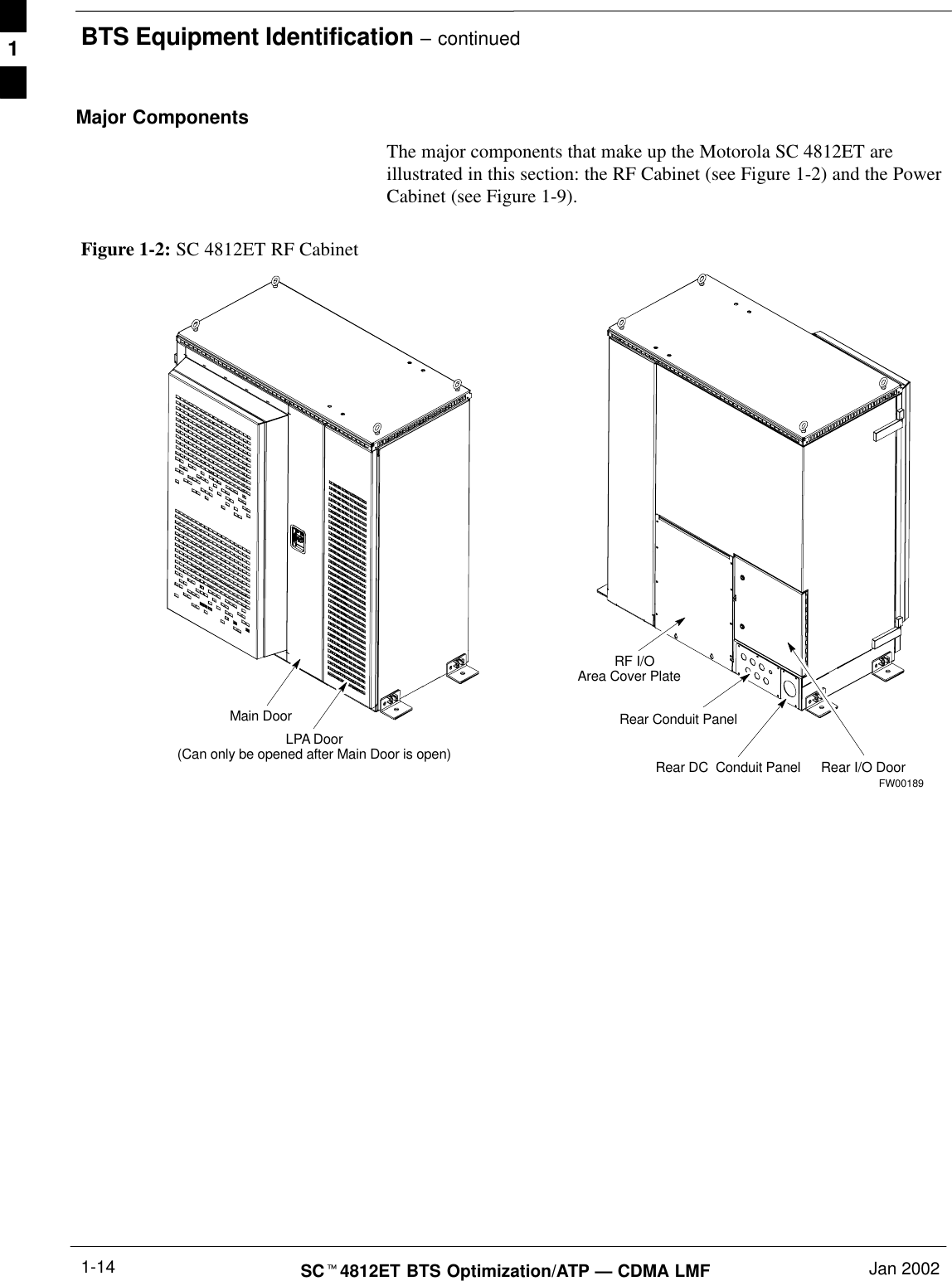
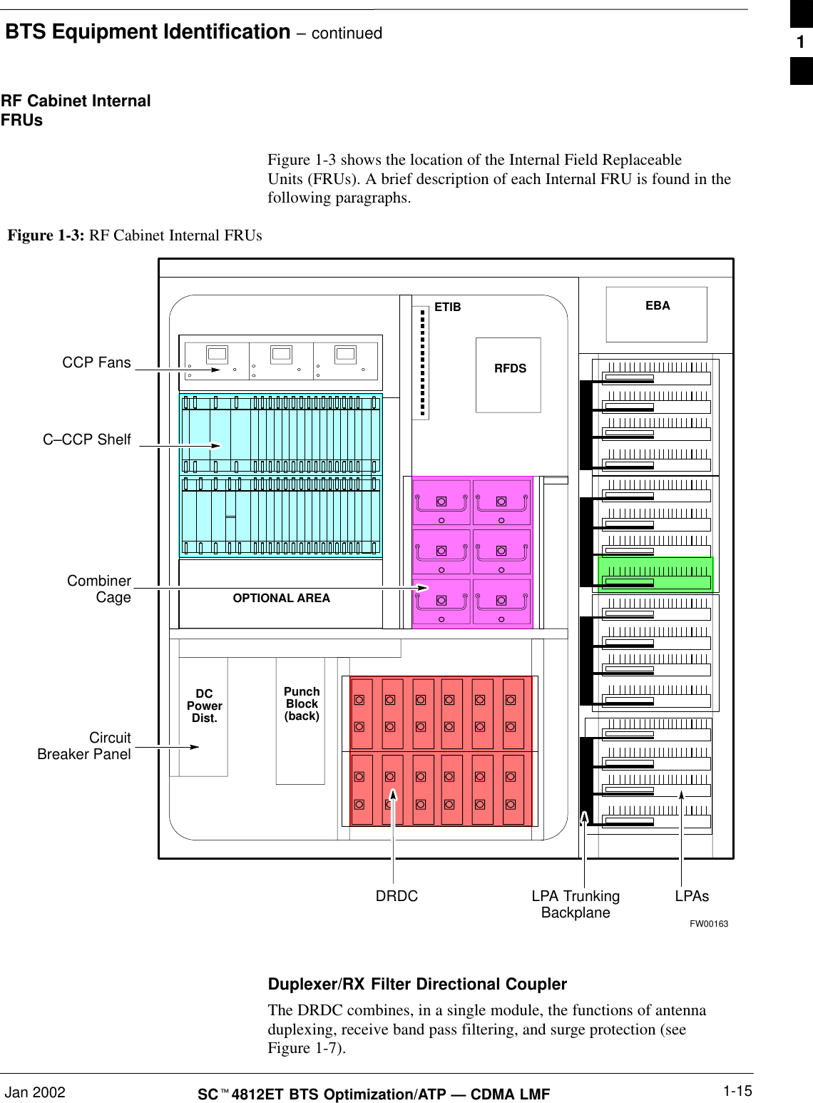
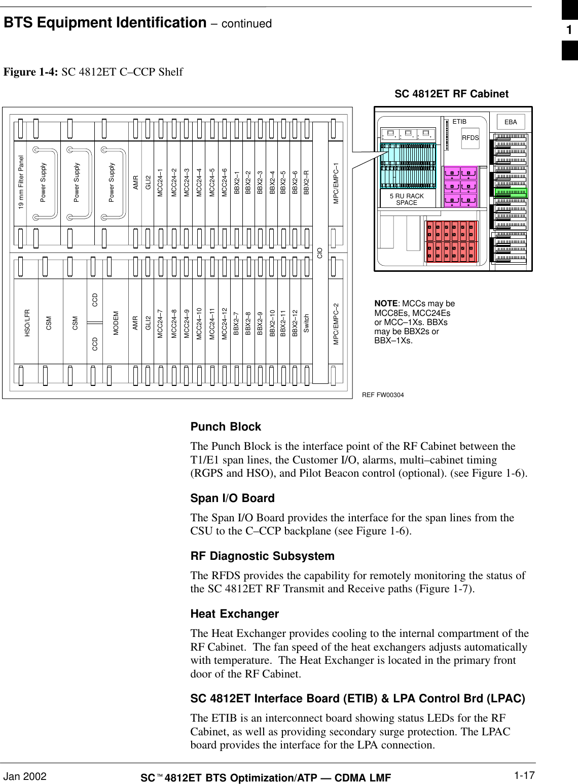
Nokia Solutions and Networks T5CT1 Cellular CDMA base station User Manual IHET5CT1 GLI2 Manual 1 of 6
Nokia Solutions and Networks Cellular CDMA base station IHET5CT1 GLI2 Manual 1 of 6
Contents
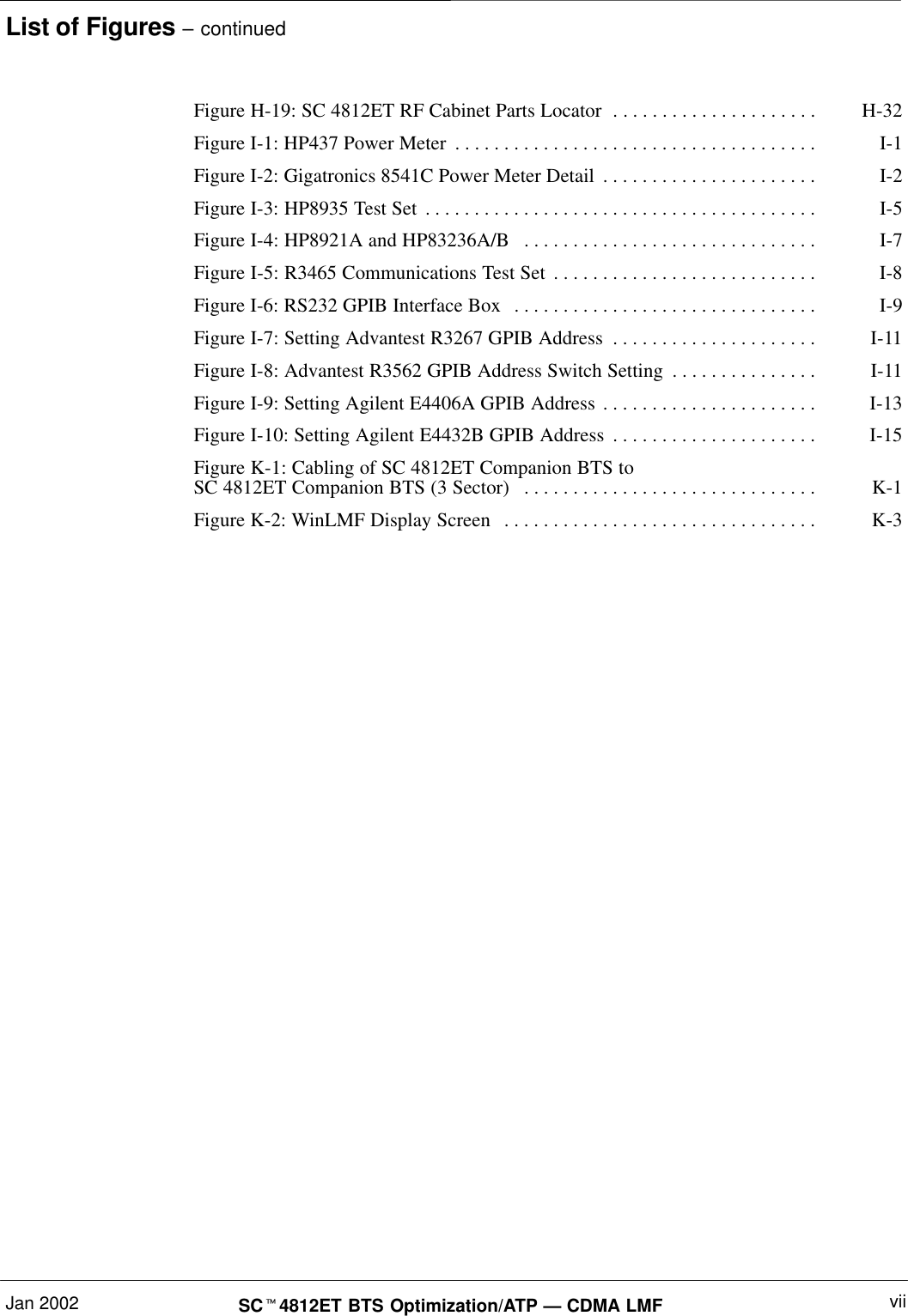
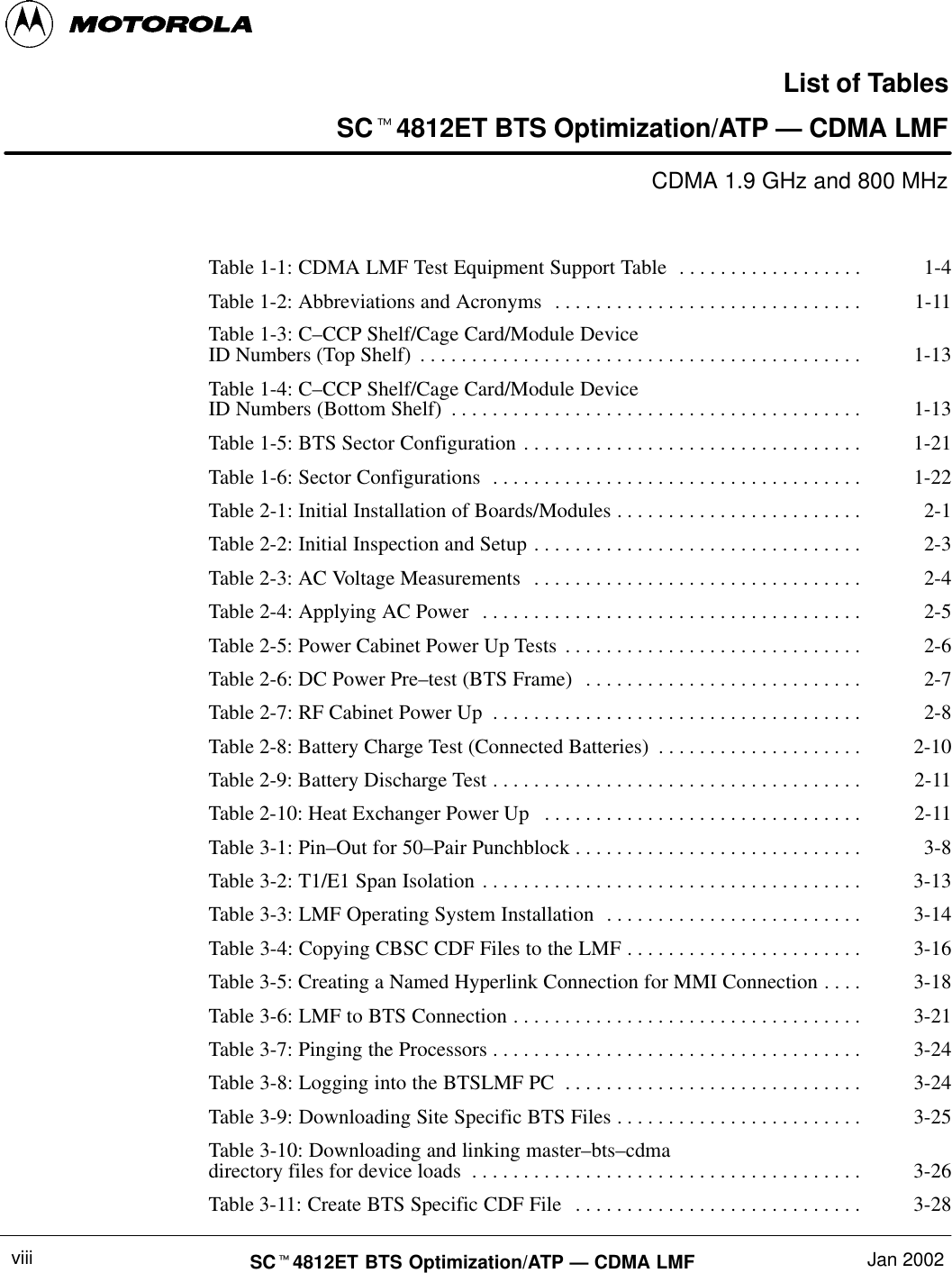
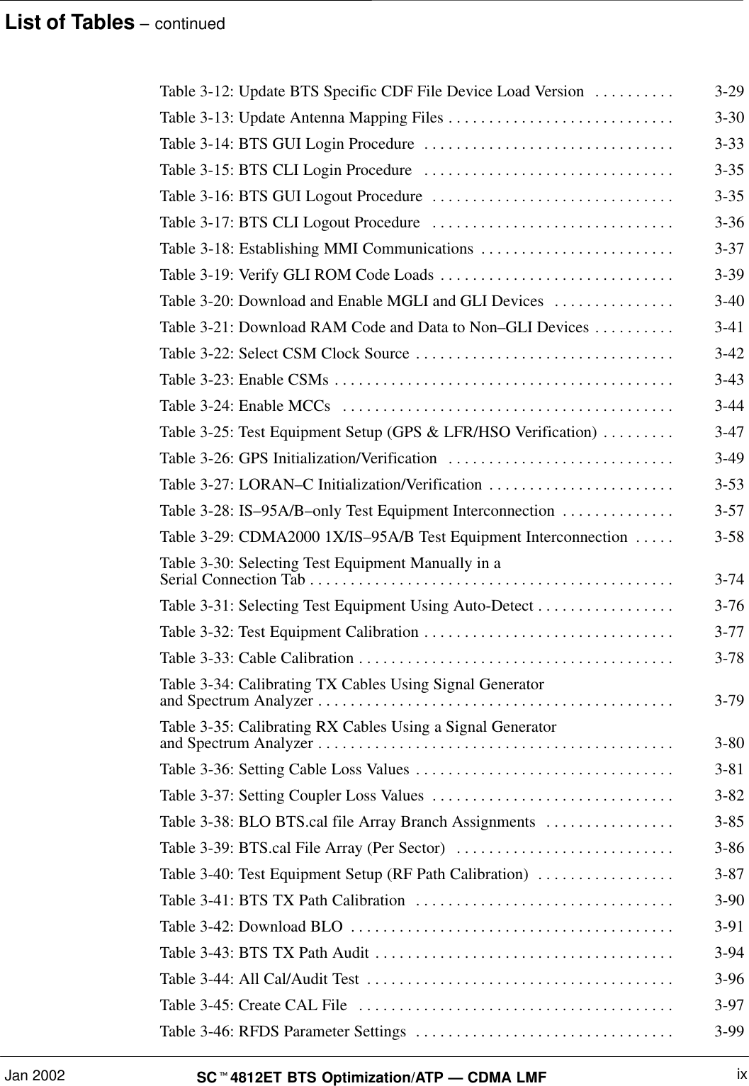
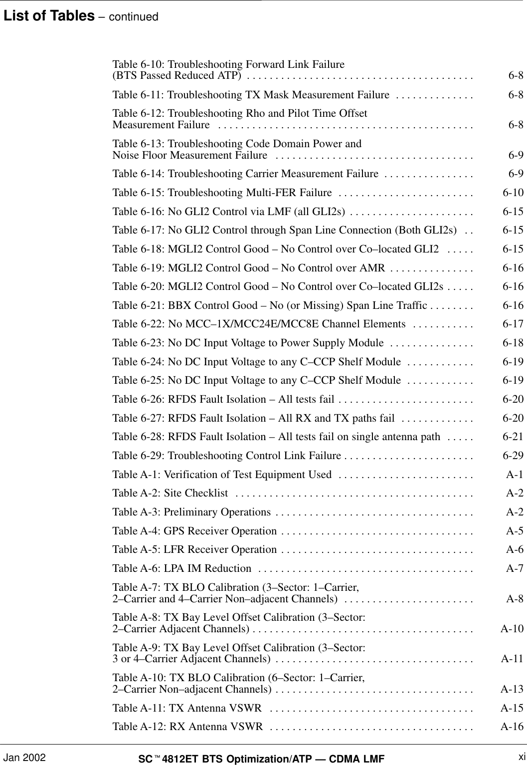
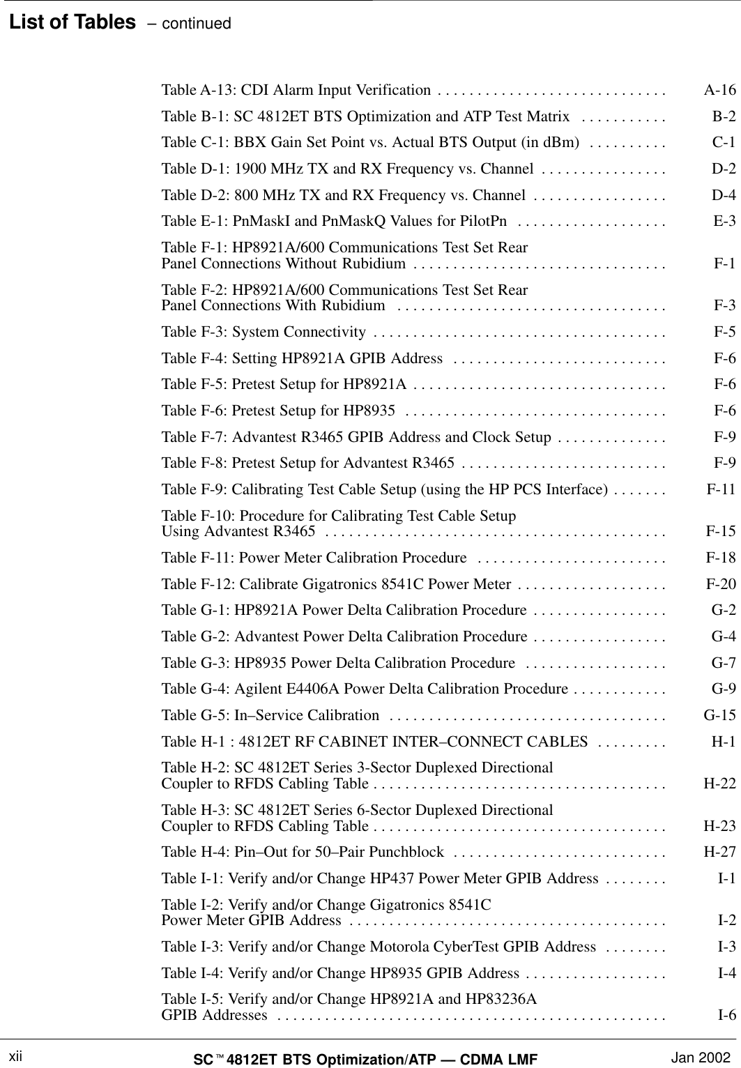
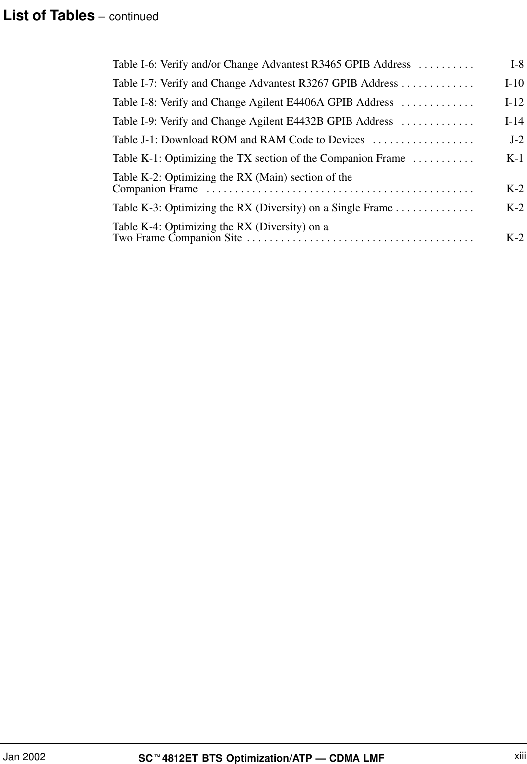
- 1. IHET5CT1 GLI2 Manual 1 of 6
- 2. IHET5CT1 GLI2 Manual 2 of 6
- 3. IHET5CT1 GLI2 Manual 3 of 6
- 4. IHET5CT1 GLI2 Manual 4 of 6
- 5. IHET5CT1 GLI2 Manual 5 of 6
- 6. IHET5CT1 GLI2 Manual 6 of 6
- 7. IHET5CT1 GLI3 Manual 1 of 6
- 8. IHET5CT1 GLI3 Manual 4 of 6
- 9. IHET5CT1 GLI3 Manual 5 of 6
- 10. IHET5CT1 GLI3 Manual 6 of 6
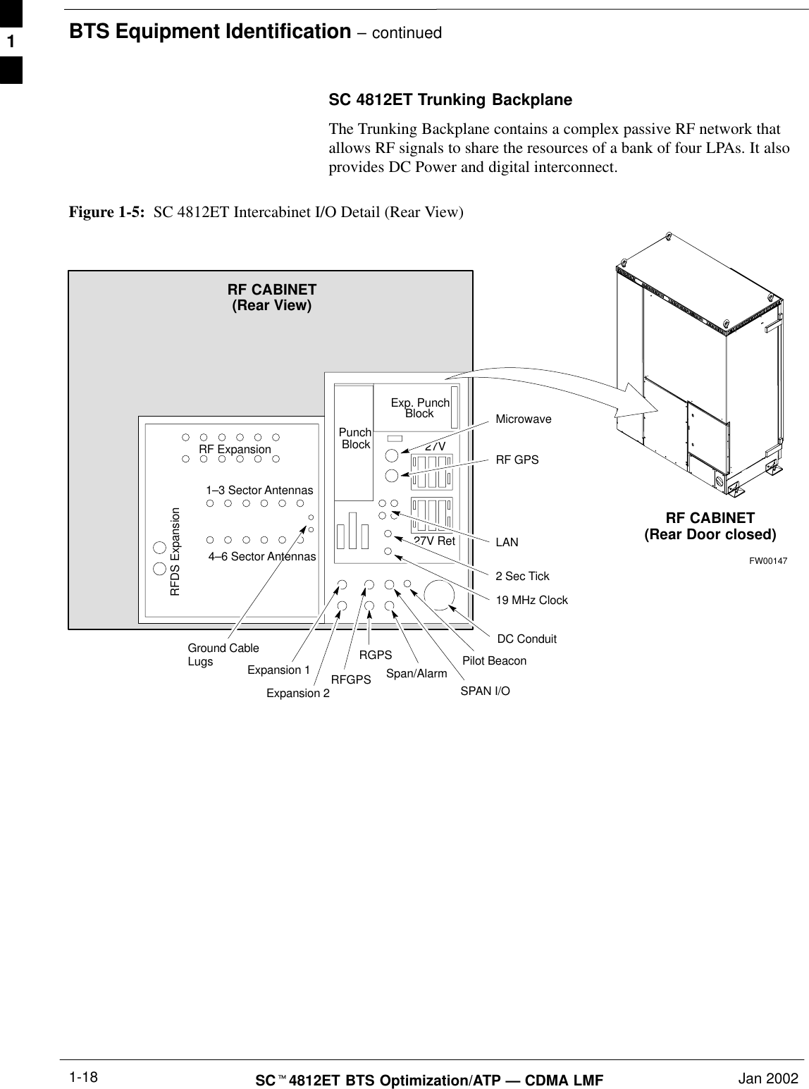
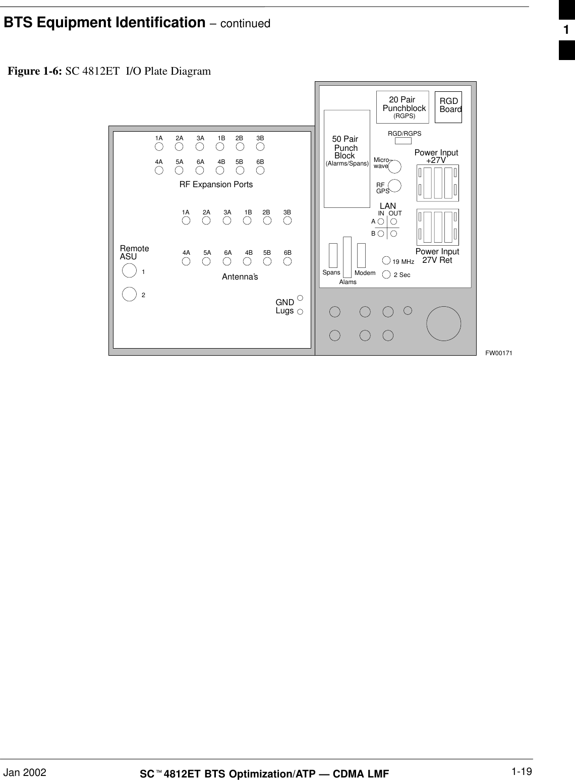
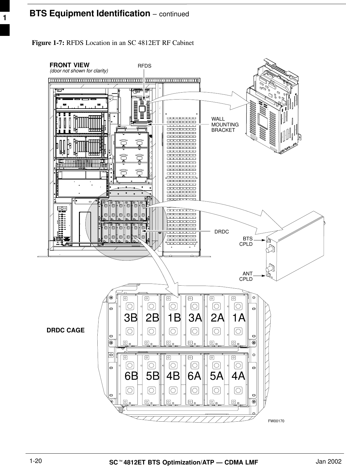
IHET5CT1 GLI2 Manual 1 of 6