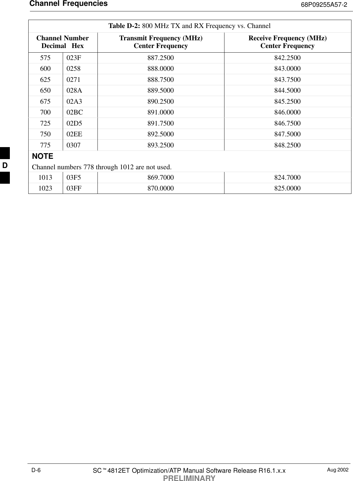
Nokia Solutions and Networks T5CT1 Cellular CDMA base station User Manual IHET5CT1 GLI3 Manual 4 of 6
Nokia Solutions and Networks Cellular CDMA base station IHET5CT1 GLI3 Manual 4 of 6
Contents
- 1. IHET5CT1 GLI2 Manual 1 of 6
- 2. IHET5CT1 GLI2 Manual 2 of 6
- 3. IHET5CT1 GLI2 Manual 3 of 6
- 4. IHET5CT1 GLI2 Manual 4 of 6
- 5. IHET5CT1 GLI2 Manual 5 of 6
- 6. IHET5CT1 GLI2 Manual 6 of 6
- 7. IHET5CT1 GLI3 Manual 1 of 6
- 8. IHET5CT1 GLI3 Manual 4 of 6
- 9. IHET5CT1 GLI3 Manual 5 of 6
- 10. IHET5CT1 GLI3 Manual 6 of 6
IHET5CT1 GLI3 Manual 4 of 6

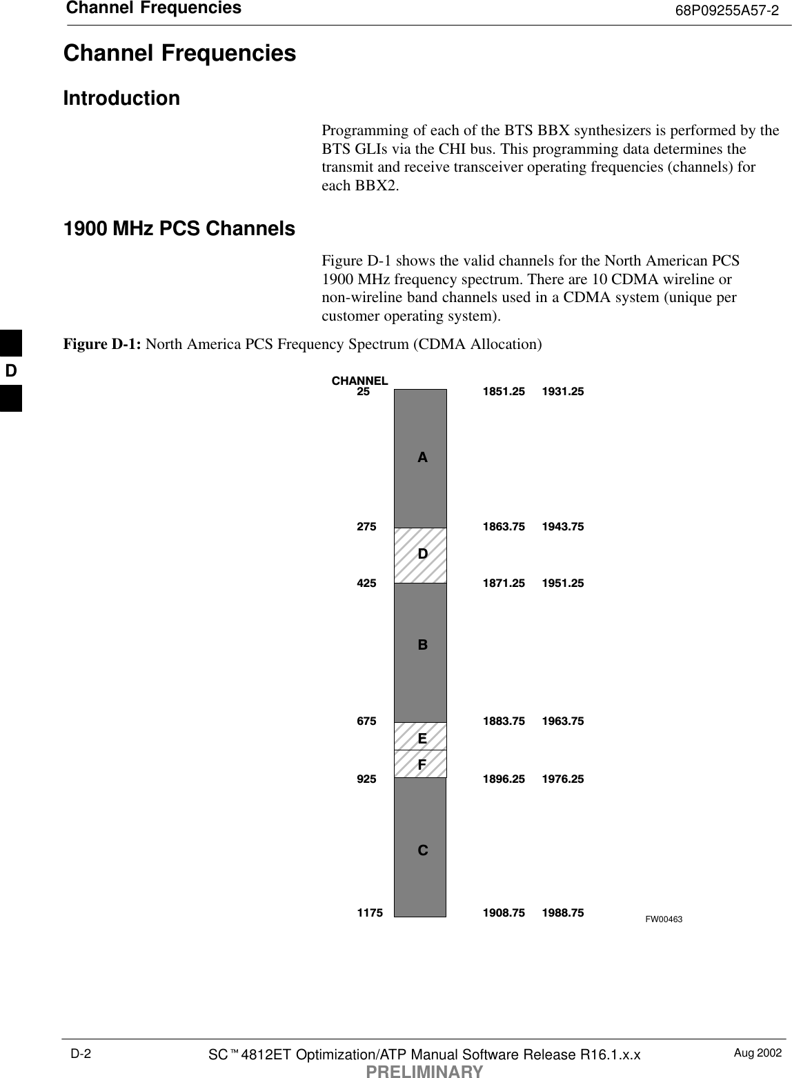
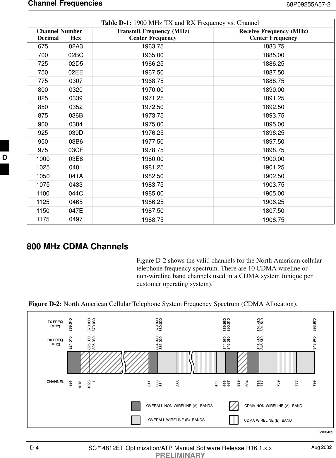


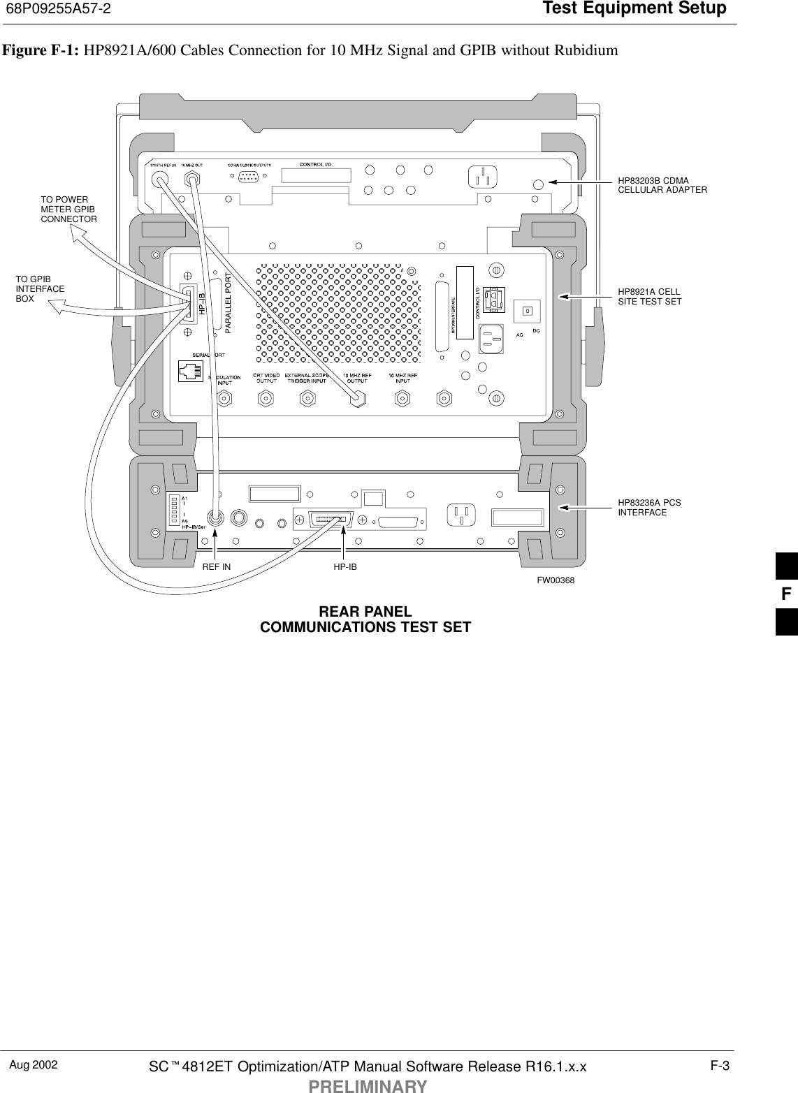
![Test Equipment Setup 68P09255A57-2Aug 2002SCt4812ET Optimization/ATP Manual Software Release R16.1.x.xPRELIMINARYF-6HP8921A System Connectivity TestFollow the steps in Table F-3 to verify that the connections between thePCS Interface and the HP8921A are correct and cables are intact. Thesoftware also performs basic functionality checks of each instrument.NOTE Disconnect other GPIB devices, especially system controllers,from the system before running the connectivity software.Table F-3: System ConnectivityStep Action* IMPORTANT- Perform this procedure after test equipment has been allowed to warm-up and stabilize for aminimum of 60 minutes.1Insert HP 83236A Manual Control/System card into memory card slot.2Press the [PRESET] pushbutton.3Press the Screen Control [TESTS] pushbutton to display the “Tests” Main Menu screen.4Position the cursor at Select Procedure Location and select it by pressing the cursor control knob. Inthe Choices selection box, select Card.5Position the cursor at Select Procedure Filename and select it by pressing the cursor control knob. Inthe Choices selection box, select SYS_CONN.6Position the cursor at RUN TEST and select it. The software will prompt you through theconnectivity setup.7Do the following when the test is complete,Sposition cursor on STOP TEST and select itSOR press the [K5] pushbutton.8To return to the main menu, press the [K5] pushbutton.9Press the [PRESET] pushbutton.Setting HP8921A and HP83236A/B GPIB AddressFollow the steps in Table F-4 to set the HP8921A GPIB address.Table F-4: Setting HP8921A GPIB AddressStep Action1If you have not already done so, turn the HP8921A power on.2Verify that the GPIB addresses are set correctly.SHP8921A HP-IB Adrs = 18, accessed by pushing LOCAL and selecting More and I/O Configureon the HP8921A/600. (Consult test equipment OEM documentation for additional info as required).SHP83236A (or B) PCS Interface GPIB address=19. Set dip switches as follows:- A1=1, A2=1, A3=0, A4=0, A5=1, HP-IB/Ser = 1F](https://usermanual.wiki/Nokia-Solutions-and-Networks/T5CT1.IHET5CT1-GLI3-Manual-4-of-6/User-Guide-280711-Page-78.png)