Realtek Semiconductor RTL8191SE 802.11b/g/n RTL8191SE miniCard User Manual
Realtek Semiconductor Corp. 802.11b/g/n RTL8191SE miniCard
Contents
User Manual

SINGLE-CHIP IEEE 802.11b/g/n WLAN
CONTROLLER with PCI EXPRESSTM
INTERFACE
DATASHEET
Rev. 0.4
26th Nov 2008
Track ID: JATR
Realtek Semiconductor Corp.
No. 2, Innovation Road II, Hsinchu Science Park, Hsinchu 300, Taiwan
Tel.: +886-3-578-0211. Fax: +886-3-577-6047
www.realtek.com.tw
RTL8191SE-GR
RTL8191SE-GR
Datasheet
Wireless LAN Network Interface Controller ii Rev.0.4
COPYRIGHT
©2008 Realtek Semiconductor Corp. All rights reserved. No part of this document may be reproduced,
transmitted, transcribed, stored in a retrieval system, or translated into any language in any form or by any
means without the written permission of Realtek Semiconductor Corp.
DISCLAIMER
Realtek provides this document “as is”, without warranty of any kind, neither expressed nor implied,
including, but not limited to, the particular purpose. Realtek may make improvements and/or changes in
this document or in the product described in this document at any time. This document could include
technical inaccuracies or typographical errors.
TRADEMARKS
Realtek is a trademark of Realtek Semiconductor Corporation. Other names mentioned in this document are
trademarks/registered trademarks of their respective owners.
USING THIS DOCUMENT
This document is intended for the software engineer’s reference and provides detailed programming
information.
Though every effort has been made to ensure that this document is current and accurate, more information
may have become available subsequent to the production of this guide. In that event, please contact your
Realtek representative for additional information that may help in the development process.
REVISION HISTORY
Revision Release Date Summary
0.4 2008/11/26 Preliminary release.

RTL8191SE-GR
Datasheet
Wireless LAN Network Interface Controller iii Rev.0.4
Table of Contents
1. GENERAL DESCRIPTION................................................................................................................................................4
2. GENERAL FEATURES ......................................................................................................................................................5
3. APPLICATION DIAGRAM...............................................................................................................................................7
3.1. SINGLE BAND 11N APPLICATION ......................................................................................................................................7
4. PIN ASSIGNMENTS...........................................................................................................................................................8
5. PIN DESCRIPTIONS..........................................................................................................................................................9
5.1. PCIE TRANSCEIVER INTERFACE......................................................................................................................................9
5.2. EEPROM INTERFACE .....................................................................................................................................................9
5.3. POWER PINS ..................................................................................................................................................................10
5.4. RF INTERFACE...............................................................................................................................................................10
5.5. LED INTERFACE............................................................................................................................................................10
5.6. CLOCK AND OTHER PINS ...............................................................................................................................................11
6. ELECTRICAL AND THERMAL CHARACTERISTICS .............................................................................................11
6.1. TEMPERATURE LIMIT RATINGS ......................................................................................................................................11
6.2. DC CHARACTERISTICS ..................................................................................................................................................11
7. MECHANICAL DIMENSIONS.......................................................................................................................................13
8. ORDERING INFORMATION..........................................................................................................................................14
List of Tables
TABLE 1. PCIE TRANSCEIVER INTERFACE.....................................................................................................................................9
TABLE 2. EEPROM INTERFACE ....................................................................................................................................................9
TABLE 3. POWER PINS .................................................................................................................................................................10
TABLE 4. LED INTERFACE...........................................................................................................................................................10
List of Figures
FIGURE 1. SINGLE BAND 11N APPLICATION DIAGRAM .................................................................................................................7
FIGURE 2. PIN ASSIGNMENTS.........................................................................................................................................................8

RTL8191E-GR
Datasheet
Wireless LAN Network Interface Controller 4 Rev.0.4
1. General Description
The Realtek RTL8191SE is a highly integrated single-chip MIMO wireless LAN (WLAN) solution for the
wireless high throughput 802.11n draft specification. It combines a MAC, a 1T2R capable baseband, and
RF in a single chip. The RTL8191SE provides complete solution for a high throughput performance
wireless client.
The RTL8191SE baseband implements multiple input, multiple output (MIMO) orthogonal frequency
division multiplexing (OFDM) with 1 transmit and 2 receive paths and is compatible with 802.11n Draft
specification 2.0. Other features include one spatial streams transmission, up to two spatial streams
reception, short guard interval (GI) of 400ns, spatial spreading, and transmission over 20 MHz and 40 MHz
bandwidth. At the receiver, extended range and good minimum sensitivity is achieved by having receiver
diversity up to 2 antennas.
For legacy compatibility, direct sequence spread spectrum (DSSS), complementary code keying (CCK)
and OFDM baseband processing are included to support all IEEE 802.11b and 802.11g data rates.
Differential phase shift keying modulation schemes, DBPSK and DQPSK with data scrambling capability,
are available along with complementary code keying to provide the data rates of 1, 2, 5.5 and 11Mbps with
long or short preamble. The high speed FFT/IFFT paths, combined with BPSK, QPSK, 16QAM, and
64QAM modulation of the individual subcarriers and rate compatible punctured convolutional coding with
coding rate of 1/2, 2/3, 3/4, and 5/6, provides the maximum data rate of 54 Mbps and 300 Mbps for IEEE
802.11g and 802.11n MIMO OFDM respectively.
The RTL8191SE builds in an enhanced signal detector, an adaptive frequency domain equalizer, and a
soft-decision Viterbi decoder to alleviate the severe multi-path effects and mutual interference in the
reception of multiple streams. For better detection quality, receive diversity with maximal-ratio-combine
(MRC) applying up to 2 receive paths are implemented. Robust interference detection and suppression are
provided to protect against bluetooth, cordless phone, and microwave oven. Receive vector diversity for
multi-stream application is implemented for efficient utilization of MIMO channel. Efficient IQ-imbalance,
DC offset, phase noise, frequency offset and timing offset compensations are provided for the radio
frequency front-end impairments. Selectable digital transmit and receiver FIR filters are provided to meet
the requirement of transmit spectrum mask and to reject the adjacent channel interference, respectively.
The RTL8191SE supports fast receiver automatic gain control (AGC) with synchronous and asynchronous
control loops among antennas, antenna diversity functions, and adaptive transmit power control function to
obtain the better performance in the analog portions of the transceiver.
The RTL8191SE MAC supports 802.11e for multimedia applications, 802.11i for security, and 802.11n for
enhanced MAC protocol efficiency. Using packet aggregation techniques such as A-MPDU with BA and
A-MSDU, protocol efficiency is significantly improved. Power saving mechanisms such as U-APSD,
APSD, and MIMO power saving reduces the power wasted during idle time, and compensates for the extra
power required to transmit MIMO OFDM. The RTL8191SE provides simple legacy and 20Mhz/40Mhz
co-existence mechanisms to ensure backward and network compatibility.

RTL8191E-GR
Datasheet
Wireless LAN Network Interface Controller 5 Rev.0.4
2. General Features
General
64-pin QFN
CMOS MAC, Baseband MIMO PHY, and RF Single Chip for IEEE 802.11b/g/n compatible WLAN
Complete 802.11n MIMO solution for 2.4GHz band
1x2 MIMO technology for extended reception robustness and exceptional throughput
Maximum Tx/Rx PHY data rate up to 75M/150Mbps using 20Mhz bandwidth, 150M/300Mbps using
40Mhz bandwidth
Compatible with 802.11n draft 2.0 specification
Backward compatible with 802.11b/g devices while operating at 802.11n data rates
Host Interface
Complies with PCI Express™ Base Specification Revision 1.1
Standards supported
802.11e QoS Enhancement (WMM, WMM-SA Client mode)
802.11h TPC, Spectrum Measurement
802.11k Radio Resource Measurement
802.11i (WPA, WPA2). Open, shared key, and pair-wise key authentication services
Cisco Compatible Extensions (CCX) for WLAN devices
MAC Features
Frame aggregation increase MAC efficiency (A-MSDU, A-MPDU)
Low latency Immediate High-Throughput Block Acknowledgement (HT-BA)
Long NAV for media reservation with CF-End for NAV release
PHY-level spoofing to enhance legacy compatibility
MIMO power saving mechanism
Channel management and co-existence
Multiple BSSID feature allowing RTL8191SE to assume multiple MAC identity when used as wireless
bridge
Supports Wake-On-WLAN via Magic Packet and wake-up frame
TXOP SIFS bursting guarantees multimedia bandwidth
Peripheral Interface
- General Purpose Input/Output (8 pins)

RTL8191E-GR
Datasheet
Wireless LAN Network Interface Controller 6 Rev.0.4
- 4-wire EEPROM control interface (93C46)
- Configurable LED pins (2)
- Configurable Bluetooth Coexistence Interface
PHY Features
IEEE 802.11n draft 2.0 MIMO OFDM
- 1 transmit and 2 receive paths (1T2R).
- 20MHz and 40MHz bandwidth transmission.
- Short Guard Interval (400ns).
DSSS with DBPSK and DQPSK, CCK modulations with long and short preamble.
OFDM with BPSK, QPSK, 16QAM, and 64QAM modulations. Convolutional coding rate: 1/2, 2/3, 3/4,
and 5/6.
Maximum data rate 54Mbps in 802.11g and 300Mbps in 802.11n.
OFDM receive diversity with MRC using up to 2 receive paths. Switch diversity used for DSSS/CCK.
Hardware antenna diversity.
Selectable digital transmit and receiver FIR filters
Programmable scaling in transmitter and receiver to trade quantization noise against increasing probability
of clipping.
Fast receiver automatic gain control (AGC).
On-chip ADC and DAC.
RTL8191E-GR
Datasheet
Wireless LAN Network Interface Controller 7 Rev.0.4
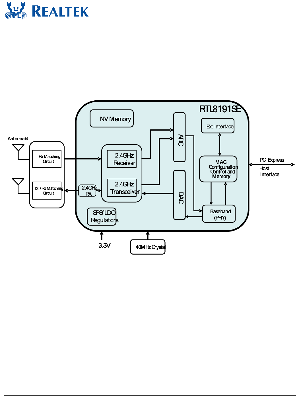
3. Application Diagram
3.1.
Single band 11n application
You can use RTL8191SE (11n 1x2 MAC/BB/RF) to support the flexible single band MIMO (1x1/1x2) solution upon your
various requirement.
RX I/Q
Antenna A TX I/Q
RX I/QRX I/Q
Antenna AAntenna A TX I/QTX I/Q
Figure 1. Single Band 11n Application Diagram
RTL8191E-GR
Datasheet
Wireless LAN Network Interface Controller 8 Rev.0.4
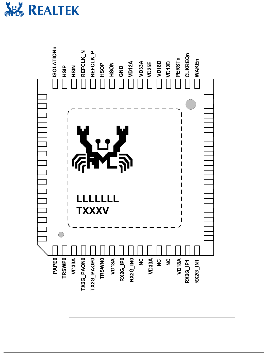
4. Pin Assignments
123456789
10 11 12 13 14 15 16
48 47 46 45 44 43 42 41 40 39 38 37 36 35 34 33
RTL8191SE
49
50
51
52
53
54
55
56
57
58
59
60
61
62
63
64
32
31
30
29
28
27
26
25
24
23
22
21
20
19
18
17
65 GND (Exposed Pad)
VD33A
RETX
BT_STATE
XI
BT_PRI
ANT_SEL_P
ANT_SEL_N
LED0
LED1
VD18A
VD15A
XO
NC
WLACT
WL_RX
GND
NC
GND
NC
VD12D
EESK
VD33A
LX
NC
VD33D
GPIO4
GPIO5
EEDI
EEDO
TSSI_0
EECS
GND
Figure 2. Pin Assignments
RTL8191E-GR
Datasheet
Wireless LAN Network Interface Controller 9 Rev.0.4
5. Pin Descriptions
In order to reduce pin count, and therefore size and cost, some pins have multiple functions. In such cases,
the functions are separated with a ‘/’ symbol. Refer to the Pin Assignments diagram on page 10 for a
graphical representation.
The following signal type codes are used in the tables:
I: Input.
O: Output
T/S: Tri-State bi-directional input/output pin.
S/T/S: Sustained Tri-State.
O/D: Open Drain.
P: Power pin.
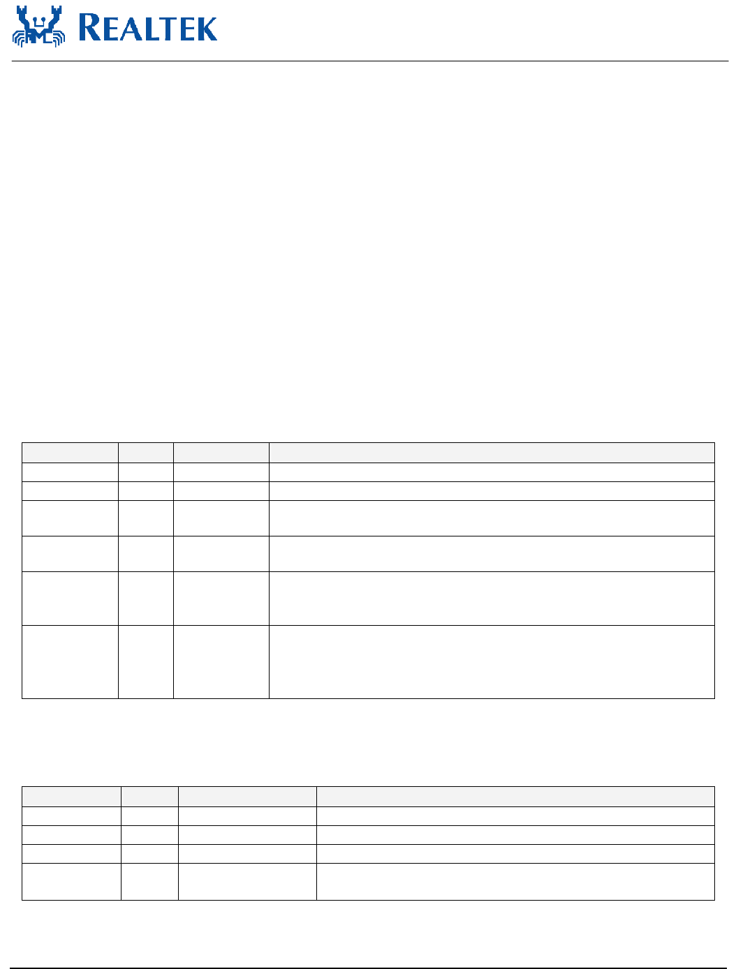
5.1.
PCIE Transceiver Interface
Table 1. PCIE Transceiver Interface
Symbol Type Pin No Description
HSIN/HSIP I 46/47 PCI Express Receive Differential Pair
HSON/HSOP O 42/43 PCI Express Transmit Differential Pair
REFCLK_P/
REFCLK_N
I 44/45 PCI Express Differential Reference Clock Source: 100MHz ± 300ppm
CLKREQn O 34 Reference clock request signal. This signal is used by the RTL8191SE-GR to
request starting of the PCI Express reference clock
WAKEn O/D 33 Power Management Event: Open drain, active low.
Used to reactivate the PCI Express slot’s main power rails and reference
clocks.
PERSTn I 35 PCI Express Reset Signal: Active low.
When the PERSTB is asserted at power-on state, the RTL8191SE-GR returns
to a pre-defined reset state and is ready for initialization and configuration
after the de-assertion of the PERSTB.
5.2.
EEPROM Interface
Table 2. EEPROM Interface
Symbol Type Pin No Description
EESK O 62 EESK in 93C46 programming or auto-load mode.
EEDI O 61 EEDI in 93C46 programming or auto-load mode.
EEDO I/O 60 EEDO in 93C46 programming or auto-load mode.
EECS O 63 EEPROM Chip Select.
93C46 chip select.
RTL8191E-GR
Datasheet
Wireless LAN Network Interface Controller 10 Rev.0.4
5.3.
Power Pins
Table 3. Power Pins
Symbol Type Pin No Description
LX P 50 Input VDD33
GND P 28,41,59 Regulator GND
VD33A P 3,11,21,39,51 VDD 3.3V for Analog.
VD12D P 36, 58 +1.2V (Digital)
VD18A P 7,15,23 VDD 1.8V for Analog.
VD15A P 24 Analog 1.5V Capacitor
VD33D P 55 VDD3.3V for Digital
VD18D P 37 VDD 1.8V for Digital.
VD12A P 40 VDD 1.2V for Analog
RETX P 22 For Bandgap and Bias
5.4.
RF Interface
Table 4. RTL8191SE-GR RF Interface
Symbol Type Pin No Description
PAPE0 O 1 2.4GHz Transmit Power Amplifier Power Enable.
TRSWP0 O 2 Transmit/Receive Path Select 0.
TX2G_ON0 O 4 RF TX positive signal to antenna A
TX2G_OP0 O 5 RF TX negative signal to antenna A
TRSWN0 O 6 Transmit/Receive Path Select 0.
RX2G_IP0 O 8 RF RX positive signal from antenna A
RX2G_IN0 O 9 RF RX negative signal from antenna A
PAPE1 O 10 2.4GHz Transmit Power Amplifier Power Enable.
RX2G_IP1 I 15 RF RX positive signal from antenna B
RX2G_IN1 I 16 RF RX negative signal from antenna B
ANT_SEL_P O 17 Antenna Control Positive signal
ANT_SEL_N O 18 Antenna Control Negative signal
TSSI_0 I 64 Transmit signal strength indication from external power amplifier
5.5.
LED Interface
Table 4. LED Interface
Symbol Type Pin No Description
LED0, 1 O 19/20 LED Pins (Active low).
RTL8191E-GR
Datasheet
Wireless LAN Network Interface Controller 11 Rev.0.4
5.6.
Clock and Other Pins
Table 6. Clock and Other Pins
Symbol Type Pin No Description
XI I 25 40MHz OSC Input.
Input of 40MHz Crystal clock reference.
XO O 26 Output of 40MHz Crystal clock reference.
ISOLATIONn I 48 This pin can externally shutdown 8191SE without extra power switch. This pin can
also support WLAN Radio off function with host interface remaining connected.
VAUXEN/EESK I 62 Weakly pull high at power on to indicate the presence of the auxiliary power on the
mainboard. Otherwise, this is for EEPROM autoload.
GPIO0/WLAN_
ACT
I/O 29 There are 8 General Purpose Input/Output pins. Some are used for power-on latch and
Bluetooth coexistence, and also EEPROM purposes.
The WLAN_ACT signal indicates when WLAN is either transmitting or receiving in
the 2.4GHz ISM band.
GPIO1/WLAN_R
X
I/O 30 Wireless LAN RX activity indicator.
GPIO2/BT_STAT
E
I/O 31 The BTSTAT signal indicates when normal Bluetooth packets are being transmitted or
received.
GPIO3/BT_PRI I/O 32 Left not connected if the EEPROM in use is 93C46.
The BTPRI signal indicates when a high priority Bluetooth packet is being transmitted
or received.
GPIO4 I/O 56 GPIO4.
GPIO5 I/O 57 GPIO5.
GPIO6/EEDO I/O 60 EEPROM interface EEDO signal.
GPIO7/EEDI I/O 61 EEPROM interface EEDI signal.
6. Electrical and Thermal Characteristics
6.1.
Temperature Limit Ratings
Table 8. Temperature Limit Ratings
Parameter Minimum Maximum Units
Storage Temperature -55 +125 °C
Ambient Operating Temperature 0 70 °C
Junction Temperature 0 125 °C
6.2.
DC Characteristics
Below is a description of the general DC specifications for the RTL8191SE.
Table 9. DC Characteristics
Symbol Parameter Conditions Minimum Typical Maximum Units
DVDD33 3.3V I/O Supply Voltage 3.135 3.3 3.465 V

RTL8191E-GR
Datasheet
Wireless LAN Network Interface Controller 12 Rev.0.4
Symbol Parameter Conditions Minimum Typical Maximum Units
DVDD18 1.8V Supply Voltage 1.71 1.8 1.89 V
DVDD12 1.2V Core Supply Voltage 1.10 1.2 1.32 V
RTL8191E-GR
Datasheet
Wireless LAN Network Interface Controller 13 Rev.0.4
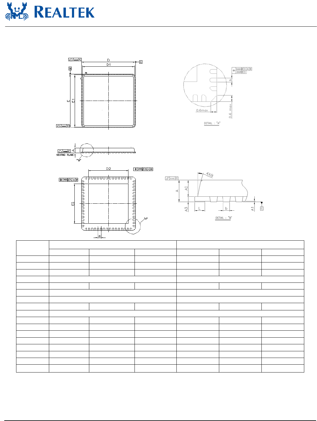
7. Mechanical Dimensions
Dimension in mm Dimension in inch
Symbol Min Nom Max Min Nom Max
A 0.75 0.85 1.00 0.030 0.034 0.039
A1 0.00 0.02 0.05 0.000 0.001 0.002
A2 0.55 0.65 0.80 0.022 0.026 0.032
A3 0.20 REF 0.008 REF
b 0.18 0.25 0.30 0.007 0.010 0.012
D/E 9.00BSC 0.354BSC
D1/E1 8.75BSC 0.344BSC
D2/E2 5.25 5.5 5.75 0.206 0.216 0.226
e 0.50BSC 0.020BSC
L 0.30 0.40 0.50 0.012 0.016 0.020
θ 0
o — 14o 0
o — 14o
aaa — — 0.15 — — 0.006
bbb — — 0.10 — — 0.004
ccc — — 0.10 — — 0.004
ddd — — 0.05 — — 0.002
eee — — 0.08 — — 0.003
fff — — 0.10 — — 0.004
Notes:
1. DIMENSIONS D1 AND E1 DO NOT INCLUDE MOLD PROTRUSION.
2. CONTROLLING DIMENSION:MILLIMETER(mm).
3. REFERENCE DOCUMENTL:JEDEC MO-220.

RTL8191E-GR
Datasheet
Wireless LAN Network Interface Controller 14 Rev.0.4
8. Ordering Information
Table 8. Ordering Information
Part Number Package Status
RTL8191SE-GR QFN-64, Green package Enineering Sample
(Blank)
Realtek Semiconductor Corp.
Headquarters
No. 2, Innovation Road II, Hsinchu Science Park,
Hsinchu, 300, Taiwan, R.O.C.
Tel: 886-3-5780211 Fax: 886-3-5776047
www.realtek.com.tw

RTL8191E-GR
Datasheet
Wireless LAN Network Interface Controller 15 Rev.0.4
FCC Statement
Federal Communication Commission Interference Statement
This equipment has been tested and found to comply with the limits for a Class B digital device, pursuant to Part 15 of
the FCC Rules. These limits are designed to provide reasonable protection against harmful interference in a
residential installation. This equipment generates, uses and can radiate radio frequency energy and, if not installed
and used in accordance with the instructions, may cause harmful interference to radio communications. However,
there is no guarantee that interference will not occur in a particular installation. If this equipment does cause harmful
interference to radio or television reception, which can be determined by turning the equipment off and on, the user is
encouraged to try to correct the interference by one of the following measures:
● Reorient or relocate the receiving antenna.
● Increase the separation between the equipment and receiver.
● Connect the equipment into an outlet on a circuit different from that to which the receiver is connected.
● Consult the dealer or an experienced radio/TV technician for help.
FCC Caution: Any changes or modifications not expressly approved by the party responsible for compliance could
void the user’s authority to operate this equipment.
This device complies with Part 15 of the FCC Rules. Operation is subject to the following two conditions: (1) This
device may not cause harmful interference, and (2) this device must accept any interference received, including
interference that may cause undesired operation.
For product available in the USA/Canada market, only channel 1~11 can be operated. Selection of other channels is
not possible.
This device and its antenna(s) must not be co-located or operation in conjunction with any other antenna or
transmitter.
FCC NOTICE: To comply with FCC part 15 rules in the United States, the system must be professionally installed to
ensure compliance with the Part 15 certification. It is the responsibility of the operator and professional installer to
ensure that only certified systems are deployed in the United States. The use of the system in any other combination
(such as co-located antennas transmitting the same information) is expressly forbidden.
IMPORTANT NOTE:
FCC Radiation Exposure Statement:
This equipment complies with FCC radiation exposure limits set forth for an uncontrolled environment. This
equipment should be installed and operated with minimum distance 20cm between the radiator & your body.
USERS MANUAL OF THE END PRODUCT:
In the users manual of the end product, the end user has to be informed to keep at least 20cm separation with the
antenna while this end product is installed and operated. The end user has to be informed that the FCC
radio-frequency exposure guidelines for an uncontrolled environment can be satisfied. The end user has to also be
informed that any changes or modifications not expressly approved by the manufacturer could void the user's
authority to operate this equipment.
The FCC part 15.19 statement below has to also be available in the manual:
This device complies with Part 15 of FCC rules. Operation is subject to the following two conditions: (1) this device
may not cause harmful interference and (2) this device must accept any interference received, including interference
that may cause undesired operation.

RTL8191E-GR
Datasheet
Wireless LAN Network Interface Controller 16 Rev.0.4
LABEL OF THE END PRODUCT:
The final end product must be labeled in a visible area with the following " Contains TX FCC ID: TX2-RTL8191SE ".
IC Statement
Country Code Statement
For product available in the USA/Canada market, only channel 1~11 can be operated. Selection of other channels is
not possible.
This device and its antenna(s) must not be co-located or operation in conjunction with any other antenna or
transmitter.
To reduce potential radio interference to other users, the antenna type and its gain should be so chosen that the
equivalent isotropically radiated power (e.i.r.p) is not more than that permitted for successful communication.
IMPORTANT NOTE:
IC Radiation Exposure Statement:
This equipment complies with IC RSS-102 radiation exposure limits set forth for an uncontrolled environment. This
equipment should be installed and operated with minimum distance 20cm between the radiator & your body.
LABEL OF THE END PRODUCT:
The final end product must be labeled in a visible area with the following " Contains TX IC: 6317A-RTL8191SE ".
This module is intended for OEM integrator. The OEM integrator is still responsible for the IC compliance
requirement of the end product, which integrates this module.
20cm minimum distance has to be able to be maintained between the antenna and the users for the host this module
is integrated into. Under such configuration, the IC RSS-102 radiation exposure limits set forth for an
population/uncontrolled environment can be satisfied.
Any changes or modifications not expressly approved by the manufacturer could void the user's authority to operate
this equipment.
This Class B digital apparatus complies with Canadian ICES-003.
Cet appareil numérique de la classe B conforme á la norme NMB-003 du Canada.
Operation is subject to the following two conditions: (1) this device may not cause interference, and (2) this device
must accept any interference, including interference that may cause undesired operation of the device.