Realtek Semiconductor RTL8191SE 802.11b/g/n RTL8191SE miniCard User Manual
Realtek Semiconductor Corp. 802.11b/g/n RTL8191SE miniCard
UserManual.wiki
>
Realtek Semiconductor
>
RTL8191SE User Manual
>
User Manual
Contents
1.
User Manual
2.
USERS MANUAL
3.
Users Manual
4.
(RTL8191SE) UserMan 0303
5.
User Manual 1
6.
User Manual 2
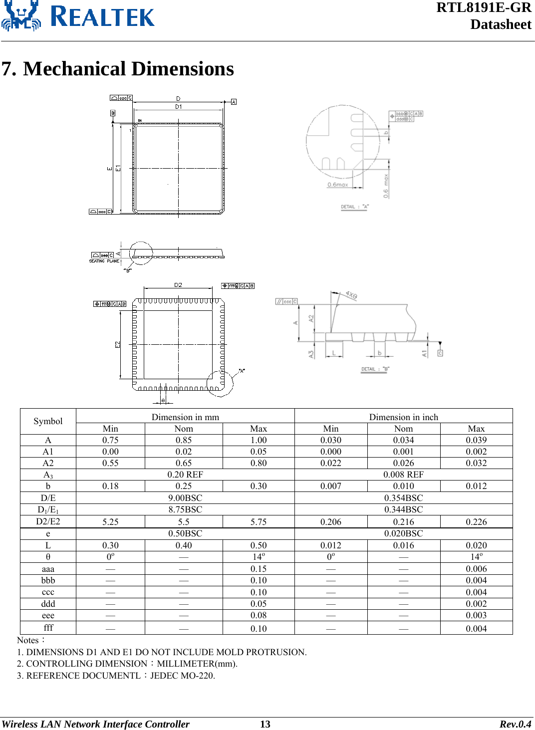
7.
User manual
User Manual
Navigation menu
Upload a User Manual
Namespaces
Wiki Guide
HTML
PDF
Info
Views
User Manual
Discussion / Help
Navigation