Simcom 1403022014008 WCDMA/HSDPA Module User Manual SIM5320AL
Shanghai Simcom Ltd. WCDMA/HSDPA Module SIM5320AL
UserManual.wiki
>
Simcom
>
1403022014008 User Manual
>
SIM5320AL_User Manual
Contents
1.
SIM5320AL_User Manual
2.
SIM5320AL_EVB_User Guide
SIM5320AL_User Manual
Navigation menu
Upload a User Manual
Namespaces
Wiki Guide
HTML
PDF
Info
Views
User Manual
Discussion / Help
Navigation

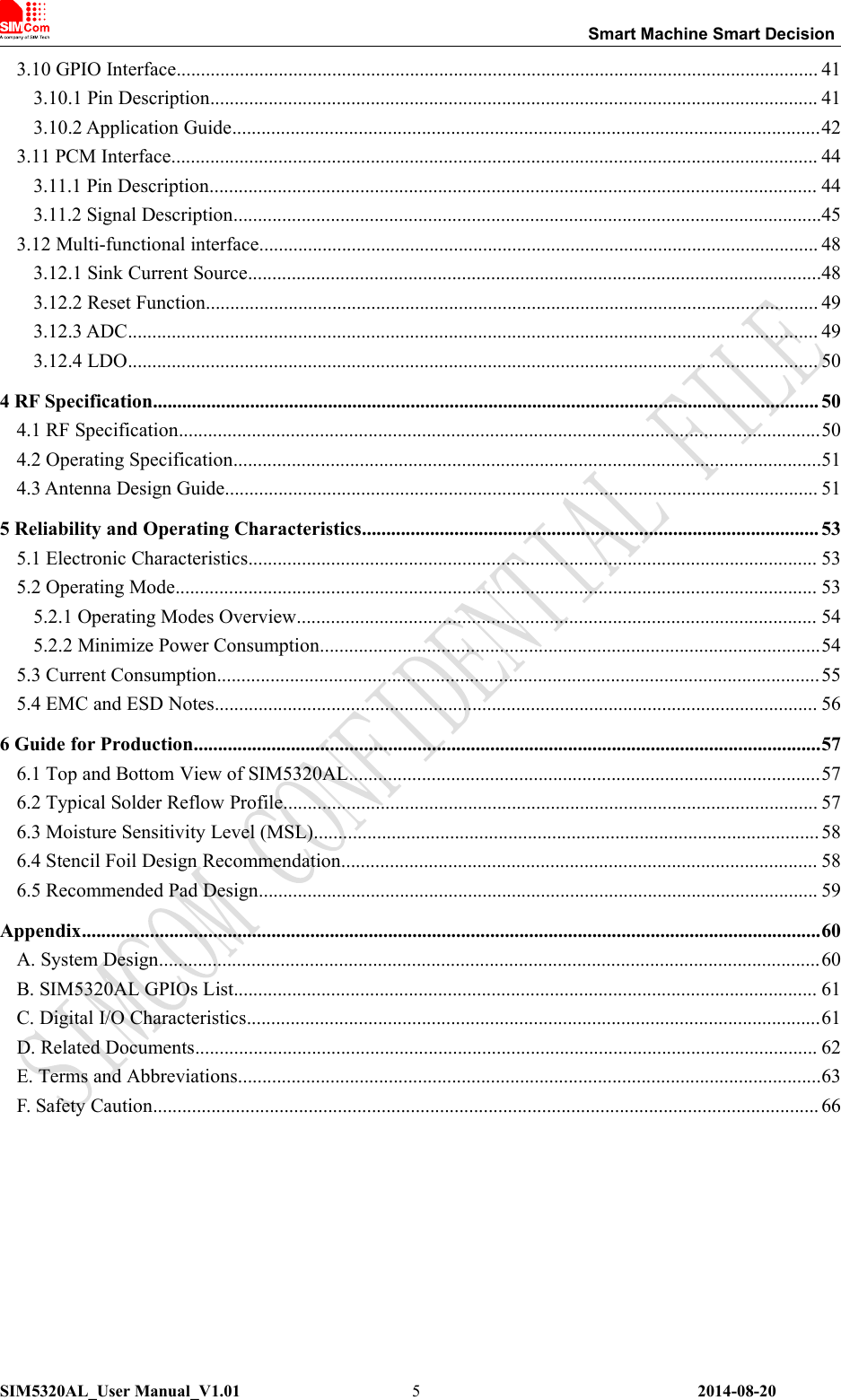
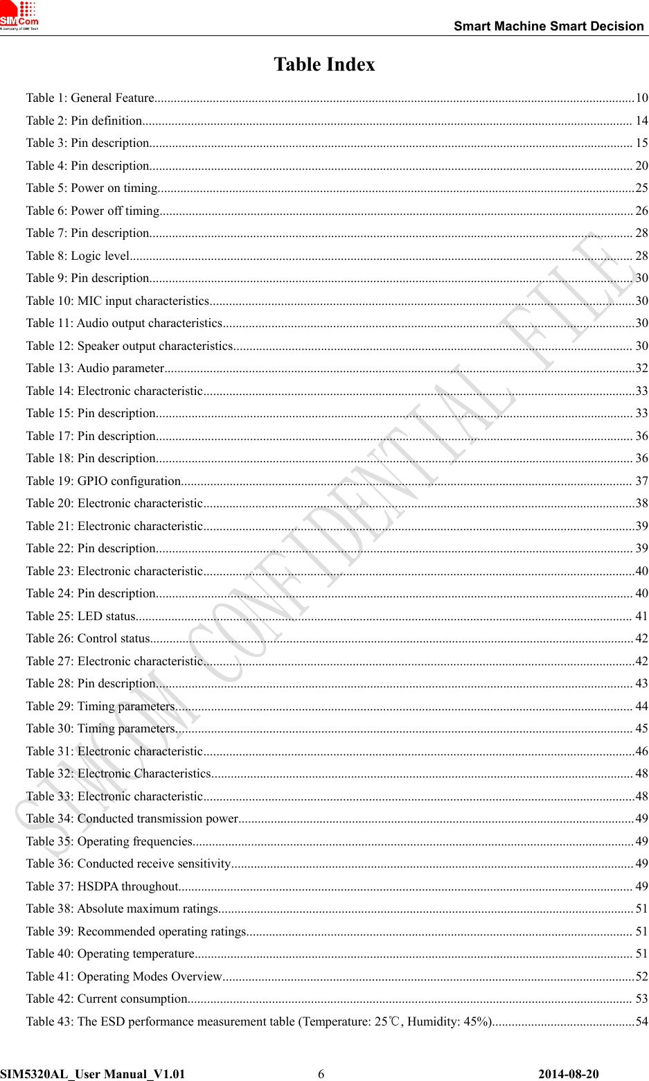
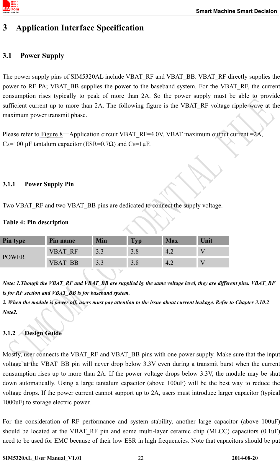
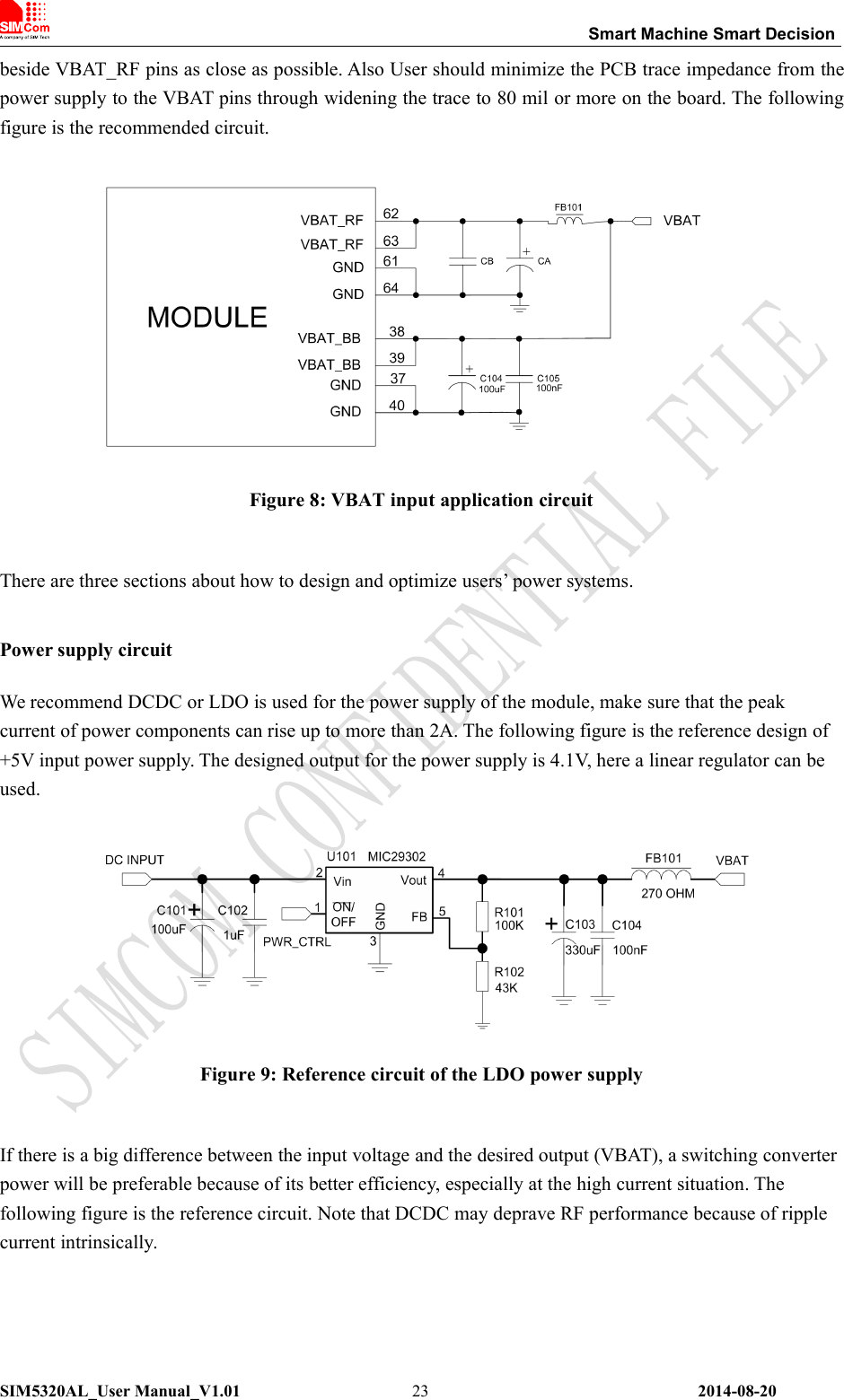
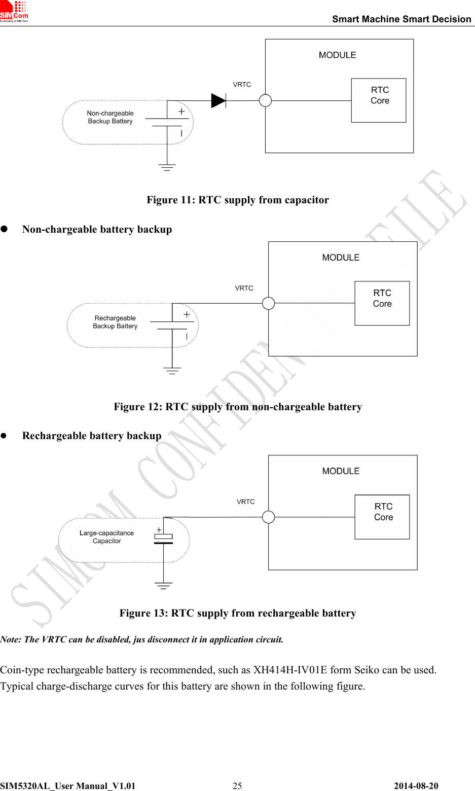
![Smart Machine Smart DecisionSIM5320AL_User Manual_V1.01 2014-08-2024Figure 10: Reference circuit of the DCDC power supplyVoltage monitorTo monitor the power supply voltage, user can use the AT command “AT+CBC”, this command has twoparameters: the battery status and the voltage value (mV). It will return the capacity percentage and actualvalue of battery (at the VBAT_BB pin). The voltage is continuously measured at intervals, whenever themeasured battery voltage is lower than a specific value set by the AT command “AT+CVALARM”. Forexample, if the voltage value is set to be 3.4V, the following URC will be presented: “warning! voltage islow: 3.3v”.If the voltage is lower than a specific value which is set by the AT command “AT+CPMVT”, the modulewill be powered off automatically and AT commands cannot be executed any more.Note: Under-voltage warning function is disabled by default, user can enable it by the AT command “AT+CVALARM”.Auto power off feature is disabled by default, user should set it by the AT command “AT+CPMVT” to an appropriatevalue. Please refer to Document [1].3.1.3 RTC BackupThe module uses RTC (Real Time Clock) to update and maintain inherent time and keeps system alive atno power supply status. The RTC power supply of module can be provided by an external capacitor or abattery (non-chargeable or rechargeable) through the VRTC. The following figures show various referencecircuits for RTC back up. The discharge current is less than 10uA. If this feature is used, please refer to theAT commands “AT+CTZU” and “AT +CTZR”.External capacitor backup](https://usermanual.wiki/Simcom/1403022014008.SIM5320AL-User-Manual/User-Guide-2391489-Page-24.png)
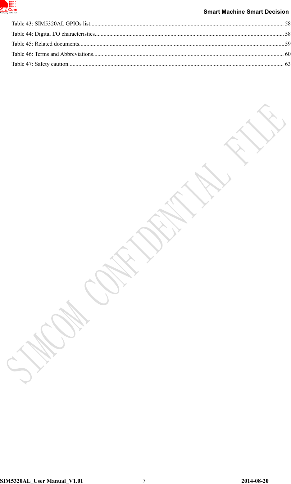
![Smart Machine Smart DecisionSIM5320AL_User Manual_V1.01 2014-08-2028Tusb The time to enable USB - - 9 sNote: Module could be automatically power on by connecting Power ON pin to Low level directly.Before designing, please refer to Document [25] for more detail.3.2.2 Power off SequenceThe following methods can be used to power down SIM5320AL. These procedures will make moduledisconnect from the network and allow the software to enter a safe state, and then save data beforecompletely powering the module off.●Method 1: Power off SIM5320AL by pulling the POWER_ON pin down●Method 2: Power off SIM5320AL by AT commandUser can power off the SIM5320AL by pulling POWER_ON down for a specific time. The power offscenario is illustrated in the following figure.Figure 16: Power off timing sequenceTable 6: Power off timingParameter Description Time valueMin. Typ. Max. UnitToff The time pulling POWER_ON down to power off 0.5 -5 s](https://usermanual.wiki/Simcom/1403022014008.SIM5320AL-User-Manual/User-Guide-2391489-Page-28.png)
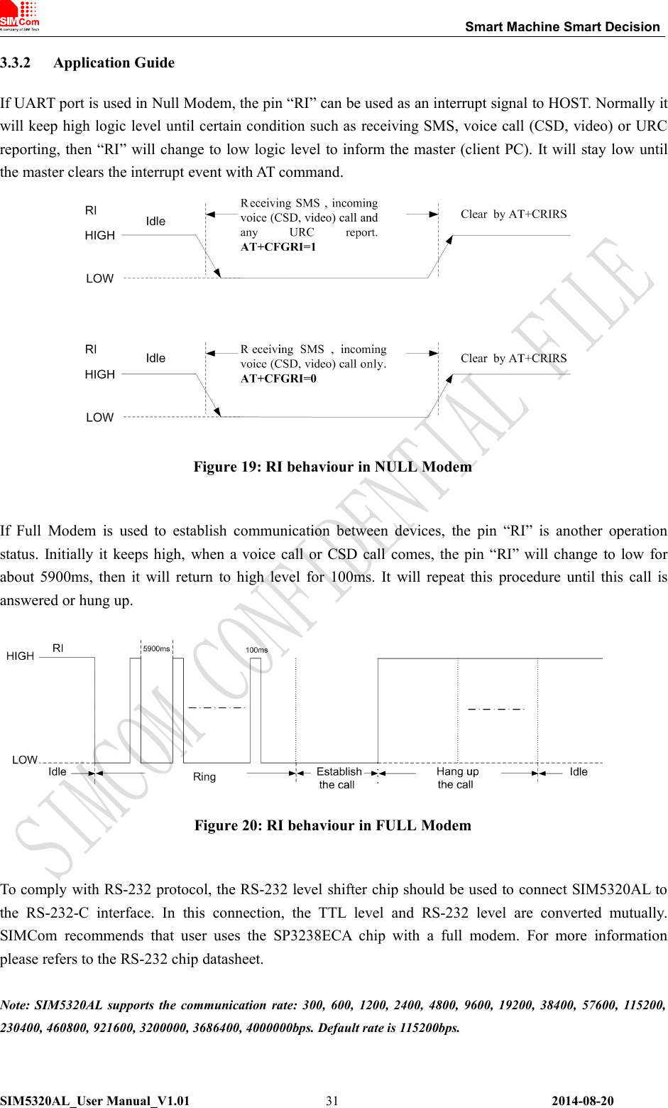
![Smart Machine Smart DecisionSIM5320AL_User Manual_V1.01 2014-08-2029TpD- The time to indicate disconnecting from the network - - 7 sTpw- The time to indicate the module power off completely - - 7.5 sTuart_off The time to disable UART - - 6 sTusb_off The time to disable USB - - 7.5 sTona The time to power on again after Tpw- 0 - - sUser can also use the AT command “AT+CPOF”to power down the module. After that, the AT commandscannot be executed any longer. The module enters the POWER DOWN mode, only the RTC is still active.For details, refer to Document [1].3.3 UART InterfaceSIM5320AL provides a UART (universal asynchronous serial transmission) port. It consists of a flexible7-wire serial interface. The module is as the DCE (Data Communication Equipment) and the client PC isas the DTE (Data Terminal Equipment). AT commands are entered and serial communication is performedthrough UART interface.In order to prevent the UART signals of the module damaged due to voltage spikes or ESD, some resistorscan be added on UART signals. The values of resistors are adjusted according to the actual circuit. Theresistors should be placed close to the module.The application circuit is in the following figures.Figure 17: Full modem](https://usermanual.wiki/Simcom/1403022014008.SIM5320AL-User-Manual/User-Guide-2391489-Page-29.png)
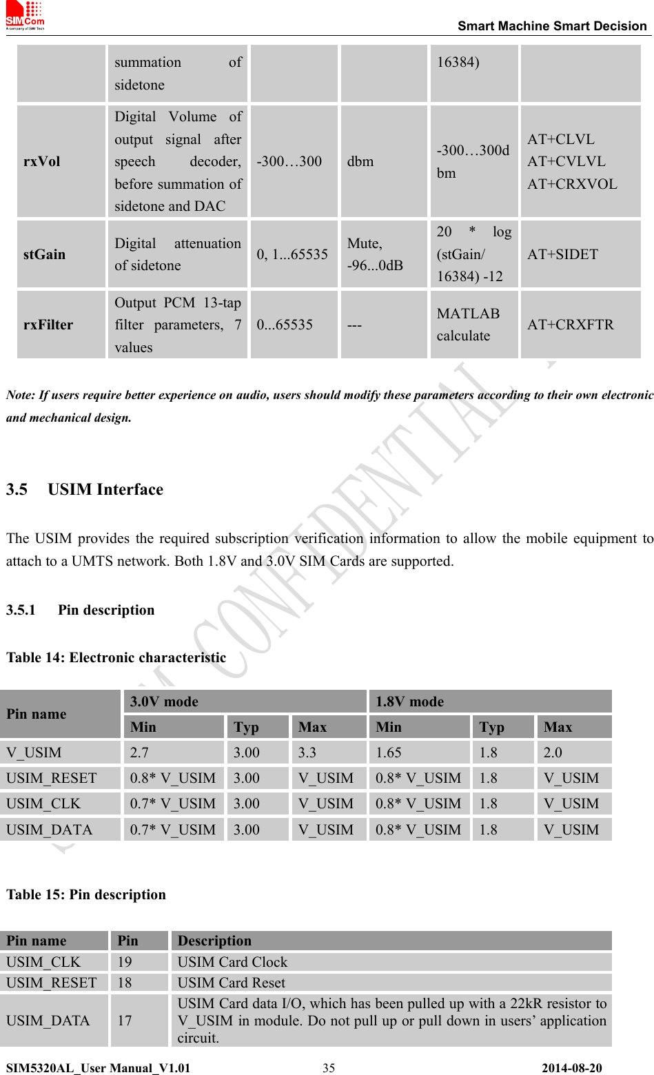
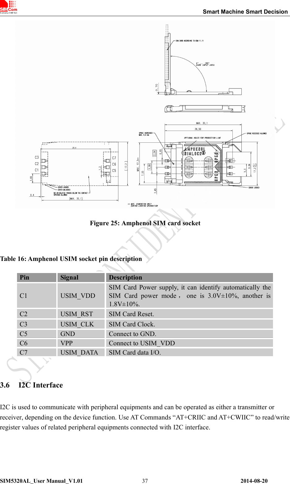
![Smart Machine Smart DecisionSIM5320AL_User Manual_V1.01 2014-08-20363.5.2 Application GuideIt is recommended to use an ESD protection component such as ST (www.st.com ) ESDA6V1W5 or ONSEMI (www.onsemi.com ) SMF05C. Note that the SIM peripheral circuit should be close to the SIM cardsocket. The reference circuit of the 8-pin SIM card holder is illustrated in the following figure.Figure 24: USIM interface reference circuitNote: USIM_DATA has been pulled up with a 22kR resistor to V_USIM in module. A 220nF shut capacitor on V_USIMis used to reduce interference. Use AT Commands to get information in USIM card. For more detail, please refer todocument [1].3.5.3 Recommend ComponentsFor 6 pins USIM socket, SIMCom recommend to use Amphenol C707 10M006 512 2. User can visithttp://www.amphenol.com for more information about the holder.V_USIM 20USIM Card Power output depends automatically on USIM mode,oneis 3.0V±10%, another is 1.8V±10%. Current is less than 50mA.](https://usermanual.wiki/Simcom/1403022014008.SIM5320AL-User-Manual/User-Guide-2391489-Page-36.png)
![Smart Machine Smart DecisionSIM5320AL_User Manual_V1.01 2014-08-2040KEYSENSE_N 0 GPIO15Note: Refer to document [21] for detailed information of Keypad Application Note.3.8 USB InterfaceSIM5320AL module contains a USB interface. This interface is compliant with the USB2.0 specification.The USB2.0 specification requires hosts such as the computer to support all three USB speeds, namelylow-speed (1.5Mbps), full-speed (12Mbps) and high-speed (480Mbps). USB charging and USB-OTG isnot supported.Table 20: Electronic characteristicPin namePin No.Input voltage scope( V )MinTypMaxUSB_VBUS114.45.05.25USB_DP13They are compliant with the USB 2.0 specification.USB_DM123.8.1 Application GuideCurrently SIM5320AL supports the USB suspend and resume mechanism which can help to save power.If no transaction is on USB bus, SIM5320AL will enter suspend mode. When some events such as voicecall or receiving SMS happen, SIM5320AL will resume normal mode automatically.Figure 27: USB interfaceBecause of high bit rate on USB bus, pay attention to influence of junction capacitance of ESD component](https://usermanual.wiki/Simcom/1403022014008.SIM5320AL-User-Manual/User-Guide-2391489-Page-40.png)
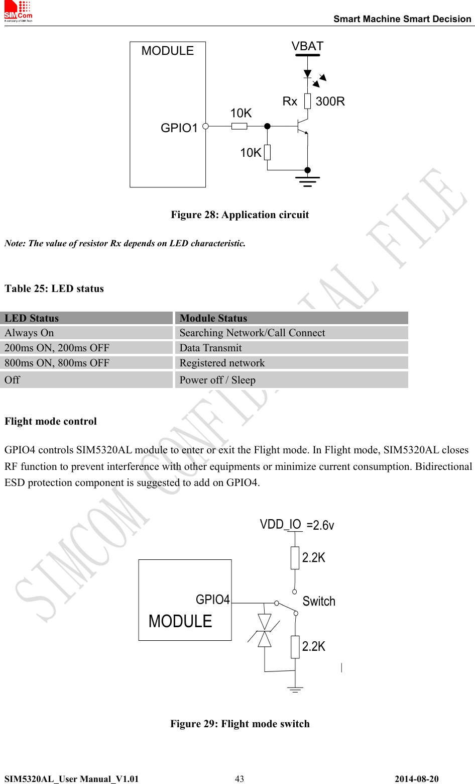
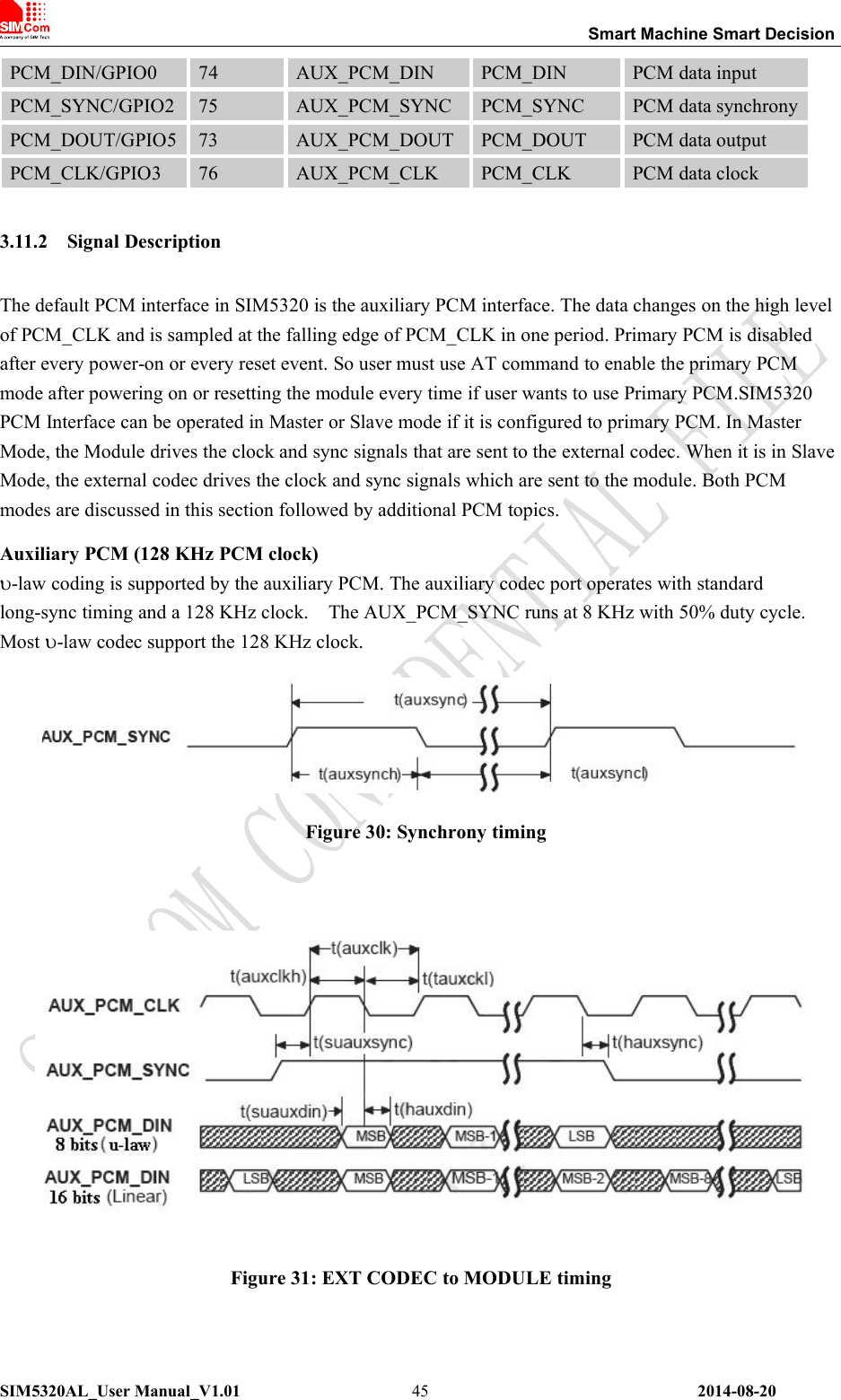
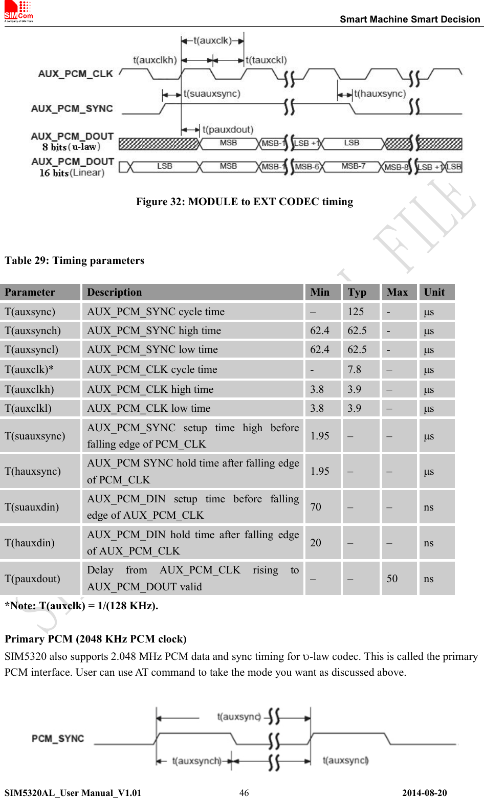
![Smart Machine Smart DecisionSIM5320AL_User Manual_V1.01 2014-08-2044Table 26: Control statusGPIO4 Status Module operationLow Level Flight Mode: RF is closed.High Level Normal Mode: RF is working.Note:1. When the module is powered off, make sure all digital interfaces (UART, etc) connected with peripheral devices haveno voltage higher than 0.3V. If users’ design cannot meet above conditions, high level voltages maybe occur in GPIOpins because current leakage from above digital interfaces may occur.3.11 PCM InterfaceSIM5320 provides hardware PCM interface for external codec. The PCM interface enablescommunication with an external codec to support hands-free applications. SIM5320 PCM interface can beused in two modes: the default mode is auxiliary PCM (8 KHz long sync mode at 128 KHz PCM CLK);the other mode is primary PCM (8 KHz short sync mode at 2048 KHz PCM CLK). In short-sync(primary PCM) mode, SIM5320 can be a master or a slave. In long-sync (auxiliary PCM) mode, SIM5320is always a master. SIM5320 also supports 3 kinds of coding formats: 8 bits (-law or A-law) and 16 bits(linear).Note: PCM interface is multiplexed from GPIO (default setting). The AT command “AT+CPCM” is used to switchbetween PCM and GPIO functions. Please refer to document [22] and document [1] for details.3.11.1 Pin DescriptionTable 27: Electronic characteristicPin name DC CharacteristicsMin Typ MaxPCM_CLK -0.3 2.6 2.9PCM_SYNC -0.3 2.6 2.9PCM_DOUT -0.3 2.6 2.9PCM_DIN -0.3 2.6 2.9Table 28: Pin descriptionPins Pin No. AUX_PCMfunctionalityPrimary PCMfunctionality Description](https://usermanual.wiki/Simcom/1403022014008.SIM5320AL-User-Manual/User-Guide-2391489-Page-44.png)
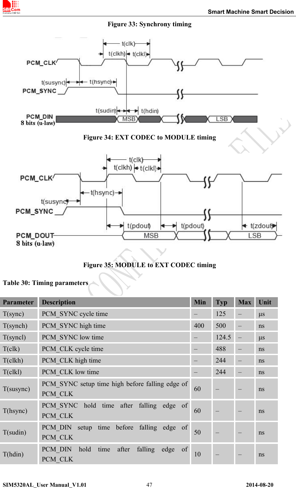
![Smart Machine Smart DecisionSIM5320AL_User Manual_V1.01 2014-08-2048T(pdout) Delay from PCM_CLK rising to PCM_DOUT valid – – 350 nsT(zdout) Delay from PCM_CLK falling to PCM_DOUTHIGH-Z – 160 – nsNote: SIM5320 can transmit PCM data by USB except for PCM interface. Please refer to document [22] for moreinformation of PCM Application Note.3.12 Multi-functional interfaceSIM5320AL merges functions for various applications. It can enrich users’ design and lower the cost ofusers’ hardware.3.12.1 Sink Current SourceThe dedicated pin (CURRENT_SINK) is intended for driving passive devices,such as LCD backlight, thisimplementation is +5V tolerant and suitable for driving white LEDs. The high-current driver can maintaina constant current which is set by the AT command “AT+ CLEDITST”, capable of up to 150 mA.Table 31: Electronic characteristicSymbol Description Min Typ Max UnitCURRENT_SINK Input voltage 0.5 VDD 5 VIOInput current - - 150 mASince the driver is ground-referenced current sink, the operating device it drives must form a current pathbetween the VDD pin and the CURRENT_SINK pin. The following figure is for users reference.Figure 36: Current drive](https://usermanual.wiki/Simcom/1403022014008.SIM5320AL-User-Manual/User-Guide-2391489-Page-48.png)
![Smart Machine Smart DecisionSIM5320AL_User Manual_V1.01 2014-08-2050User can introduce a signal in the ADC pin directly and use the AT command “AT+CADC” to get the rawdata which is between 0 and 4095. The data can be transformed to any type such as voltage, temperatureetc. Please refer to document [1].Figure 38: Reference circuitNote: The input signal voltage value in ADC must not be higher than 2.2V.3.12.4 LDOSIM5320AL has a LDO power output, namely VREG_AUX. The LDO is available and output voltage is2.85v by default, rated for 250mA. User can switch the LDO on or off by the AT command“AT+CVAUXS” and configure its output voltage by the AT command “AT+CVAUXV”.Table 33: Electronic characteristicSymbol Description Min Typ Max UnitVREG_AUX Output voltage 1.5 2.85 3.05 VIOOutput current - - 250 mA4 RF Specification4.1 RF SpecificationTable 34: Conducted transmission powerFrequency Max MinWCDMA 1900 24dBm +1/-3dB -56dBm ±5dBWCDMA 850 24dBm +1/-3dB -56dBm ±5dBTable 35: Operating frequencies](https://usermanual.wiki/Simcom/1403022014008.SIM5320AL-User-Manual/User-Guide-2391489-Page-50.png)
![Smart Machine Smart DecisionSIM5320AL_User Manual_V1.01 2014-08-2055wake up the host CPU. Before designing, pay attention to how to realize waking function and refer to Document[24] andDocument[25] for more detail.Minimum functionality modeMinimum functionality mode ceases a majority function of module, thus minimizing the powerconsumption. This mode is set by the AT command which provides a choice of the functionality levels.●AT+CFUN=0: Minimum functionality●AT+CFUN=1: Full functionality (Default)●AT+CFUN=4: Disable RF function of the module (Flight mode)If SIM5320AL has been set to minimum functionality mode, the module will firstly enter sleep mode, thenthe RF function and SIM card function will be closed. In this case, the serial port is still accessible, but RFfunction or SIM card will be unavailable. When SIM5320AL is in minimum functionality or flight mode,it can return to full functionality by the AT command “AT+CFUN=1”.Note: For flight mode, please refer to Chapter3.9.2.5.3 Current ConsumptionThe current consumption in suspended mode and without USB connection is listed in the table below.Here, “suspended mode” means that SIM5320AL is connected to USB bus, but it does not transfer data.Table 42: Current consumptionUMTS Sleep Mode (without USB connection)WCDMA 1900Sleep @DRX=9 2.2mASleep @DRX=8 2.7 mASleep @DRX=6 4.7mAWCDMA 850Sleep @DRX=9 2.2mASleep @DRX=8 2.7 mASleep @DRX=6 4.7mAUMTS Sleep Mode (with USB suspended)WCDMA 1900Sleep @DRX=9 2.4mASleep @DRX=8 2.8 mASleep @DRX=6 4.8mAWCDMA 850Sleep @DRX=9 2.4mASleep @DRX=8 2.8 mASleep @DRX=6 4.8mAHSDPA DataWCDMA 1900 @Power 23dBm CQI=22 Typical 610mA@Power 21dBm CQI=5 Typical 540mA](https://usermanual.wiki/Simcom/1403022014008.SIM5320AL-User-Manual/User-Guide-2391489-Page-55.png)
![Smart Machine Smart DecisionSIM5320AL_User Manual_V1.01 2014-08-2058Figure 41: The ramp-soak-spike reflow profile of SIM5320ALFor details about secondary SMT, please refer to document [24].6.3 Moisture Sensitivity Level (MSL)SIM5320AL is qualified to Moisture Sensitivity Level (MSL) 5 in accordance with JEDEC J-STD-020.After the prescribed time limit exceeded, users should bake modules for 192 hours in drying equipment(<5% RH) at 40° C +5° C/-0° C, or 72 hours at 85° C +5° C/-5° C. Note that plastic tray is notheat-resistant, users must not use the tray to bake at 85° C or the tray may be damaged.6.4 Stencil Foil Design RecommendationThe recommended thickness of stencil foil is more than 0.15mm.](https://usermanual.wiki/Simcom/1403022014008.SIM5320AL-User-Manual/User-Guide-2391489-Page-58.png)
![Smart Machine Smart DecisionSIM5320AL_User Manual_V1.01 2014-08-2062IIHInput highleakagecurrent- - 1 - - 1 uAIILInput lowleakagecurrent-1 - - -1 - - uACINInputcapacitance - - 7 - - 7 pFNote: These parameters are for digital interface pins, such as keypad, GPIO, I2C, UART, SPI and DEBUG. TheSIM5320AL includes two kinds of voltages: 1.8v and 2.6v. Digital I/O specifications under both conditions are presentedin the above tables.D. Related DocumentsTable 45: Related documentsSN Document name Remark[1] SIM5320AL_ATC_V1.00SIM5320AL_ATC_V1.00[2] ITU-T Draft newrecommendationV.25ter Serial asynchronous automatic dialing and control[3] GSM 07.07 Digital cellular telecommunications (Phase 2+); AT command setfor GSM Mobile Equipment (ME)[4] GSM 07.10 Support GSM 07.10 multiplexing protocol[5] GSM 07.05Digital cellular telecommunications (Phase 2+); Use of DataTerminal Equipment – Data Circuit terminating Equipment (DTE –DCE) interface for Short Message Service (SMS) and CellBroadcast Service (CBS)[6] GSM 11.14Digital cellular telecommunications system (Phase 2+);Specification of the SIM Application Toolkit for the SubscriberIdentity Module – Mobile Equipment (SIM – ME) interface[7] GSM 11.11Digital cellular telecommunications system (Phase 2+);Specification of the Subscriber Identity Module – MobileEquipment (SIM – ME) interface[8] GSM 03.38 Digital cellular telecommunications system (Phase 2+); Alphabetsand language-specific information[9] GSM 11.10Digital cellular telecommunications system (Phase 2) ;MobileStation (MS) conformance specification ;Part 1: Conformancespecification[10] 3GPP TS 51.010-1 Digital cellular telecommunications system (Release 5); MobileStation (MS) conformance specification[11] 3GPP TS 34.124 Electromagnetic Compatibility (EMC) for mobile terminals andancillary equipment.[12] 3GPP TS 34.121 Electromagnetic Compatibility (EMC) for mobile terminals andancillary equipment.](https://usermanual.wiki/Simcom/1403022014008.SIM5320AL-User-Manual/User-Guide-2391489-Page-62.png)
![Smart Machine Smart DecisionSIM5320AL_User Manual_V1.01 2014-08-2063[13] 3GPP TS 34.123-1Technical Specification Group Radio Access Network; Terminalconformance specification; Radio transmission and reception(FDD)[14] 3GPP TS 34.123-3 User Equipment (UE) conformance specification; Part 3: AbstractTest Suites.[15] EN 301 908-02 V2.2.1Electromagnetic compatibility and Radio spectrum Matters(ERM); Base Stations (BS) and User Equipment (UE) forIMT-2000. Third Generation cellular networks; Part 2:Harmonized EN for IMT-2000, CDMA Direct Spread(UTRA FDD) (UE) covering essential requirements of article3.2 of the R&TTE Directive[16] EN 301 489-24 V1.2.1Electromagnetic compatibility and Radio Spectrum Matters (ERM);Electromagnetic Compatibility (EMC) standard for radioequipment and services; Part 24: Specific conditions for IMT-2000CDMA Direct Spread (UTRA) for Mobile and portable (UE) radioand ancillary equipment[17] IEC/EN60950-1(2001) Safety of information technology equipment (2000)[18] 3GPP TS 51.010-1 Digital cellular telecommunications system (Release 5); MobileStation (MS) conformance specification[19] GCF-CC V3.23.1 Global Certification Forum - Certification Criteria[20] 2002/95/ECDirective of the European Parliament and of the Council of 27January 2003 on the restriction of the use of certain hazardoussubstances in electrical and electronic equipment (RoHS)[21] Keypad ApplicationNote V1.01 Keypad Application Note V1.01[22] Sleep_Application_Note Sleep_Application_Note[23] Waking_up_Application_NoteWaking_up_Application_Note[24] Modulesecondary-SMT-UGDSMT Note[25] SIM5xxx_Automatic_power_on_Application_NoteSIM5xxx_Automatic_power_on_Application_NoteE. Terms and AbbreviationsTable 46: Terms and AbbreviationsAbbreviation DescriptionADC Analog-to-Digital ConverterARP Antenna Reference PointBER Bit Error RateBTS Base Transceiver StationCS Coding SchemeCSD Circuit Switched DataCTS Clear to SendDAC Digital-to-Analog ConverterDRX Discontinuous Reception](https://usermanual.wiki/Simcom/1403022014008.SIM5320AL-User-Manual/User-Guide-2391489-Page-63.png)