Thales ATM 435 LICENSED NON-BROADCAST TRANSMITTER User Manual USERS MANUAL 1
Thales ATM LICENSED NON-BROADCAST TRANSMITTER USERS MANUAL 1
Contents
- 1. USERS MANUAL 1
- 2. USERS MANUAL 2
USERS MANUAL 1

THALES Italia S.p.A.- Air Systems Division
Description, Installation, Operation, Maintenance Reference: Vol. 1 Code 955 900 031C
GROUND BEACON
DME 415/435
Technical Manual
VOLUME 1
Equipment description, Installation, Operation, Maintenance and PC user
Vers. D, September 2005
SECTION 1
GENERAL INFORMATION

955 900 031C DME 415/435 -Technical Manual
Vol. 1-Section 1-General Information
1-II THALES Italia S.p.A.- A. S. D. Vers. D, September 2005

DME 415/435 -Technical Manual
Vol. 1-Section 1-General Information 955 900 031C
Vers. D, September 2005 THALES Italia S.p.A.- A. S. D. 1-a
Table of CONTENTS
Paragraph Page
SECTION 1............................................................................................................................................1-1
GENERAL INFORMATION....................................................................................................1-1
1.1 INTRODUCTION ..............................................................................................................1-1
1.2 DME PRINCIPLE ..............................................................................................................1-1
1.2.1 Coverage ..........................................................................................................................1-2
1.2.2 Traffic Capacity .................................................................................................................1-2
1.2.3 Accuracy ...........................................................................................................................1-2
1.2.4 Nominal Reply Delay – Pair Pulse Code - Channeling.....................................................1-2
1.3 GENERAL FEATURES OF THE EQUIPMENT................................................................1-13
1.3.1 Equipment Versions..........................................................................................................1-13
1.3.2 Main Feature of the Equipment ........................................................................................1-13
1.3.2.1 Engineering.......................................................................................................................1-14
1.3.2.2 Safety................................................................................................................................1-14
1.3.2.3 Installation.........................................................................................................................1-14
1.3.2.4 Operation ..........................................................................................................................1-14
1.4 BEACON COMPOSITION AND IDENTIFICATION..........................................................1-16
1.5 PHYSICAL AND MECHANICAL general Description.......................................................1-19
1.6 EQUIPMENT FUNCTIONAL DESCRIPTION...................................................................1-26
1.6.1 General Overview .............................................................................................................1-26
1.6.2 DME 415/435 System Functional Description ..................................................................1-27
1.6.3 I/O SYSTEM - Functional description ...............................................................................1-31
1.6.3.1 I/O Local site .....................................................................................................................1-31
1.6.3.2 LOCAL CONTROL & STATUS UNIT (LCSU) ..................................................................1-34
1.6.3.2.1 CONTROL AND STATUS BOARD - CSB module – Functional description....................1-36
1.6.3.2.1.1 CPU and Memories...........................................................................................................1-37
1.6.3.2.1.2 Serial Lines .......................................................................................................................1-40
1.6.3.2.1.3 Parallel ports .....................................................................................................................1-41
1.6.3.2.2 LOCAL FRONT CONTROL PANEL .................................................................................1-44
1.6.3.2.2.1 INDICATION AND CONTROLS - INC Module - functional description............................1-45
1.6.3.3 REMOTE CONTROL SYSTEM ........................................................................................1-48
1.6.3.3.1 Remote Control & Status Indicator (RCSI 446) ................................................................1-50
1.6.3.3.2 Remote Control and Status Equipment (RCSE)...............................................................1-51
1.6.3.3.3 MCS ..................................................................................................................................1-52
1.6.3.4 Status Indicator SI 446......................................................................................................1-53
1.6.3.5 Personal Computer - PC...................................................................................................1-54
1.6.4 TRANSPONDER – Functional description .......................................................................1-55
1.6.4.1 General Overviews ...........................................................................................................1-55
1.6.4.1.1 Pilot Pulse .........................................................................................................................1-55
1.6.4.1.2 Transponder Main Delay Measurement ...........................................................................1-55
1.6.4.2 RECEIVER - RX module...................................................................................................1-60
1.6.4.2.1 UHF coupler (pilot pulse mixer) and 63 MHz Oscillator....................................................1-61
1.6.4.2.2 UHF Front End & 63 MHz linear amplification..................................................................1-61
1.6.4.2.3 Synthesizer .......................................................................................................................1-62
1.6.4.2.4 Programmable attenuators ...............................................................................................1-62
1.6.4.2.5 Logarithmic Amplifier ........................................................................................................1-63
1.6.4.2.6 On channel validation (OCV) ............................................................................................1-63
1.6.4.2.7 RX reference power supply ..............................................................................................1-63
1.6.4.2.8 Digital circuitry and data bus,............................................................................................1-64

955 900 031C DME 415/435 -Technical Manual
Vol. 1-Section 1-General Information
1-b THALES Italia S.p.A.- A. S. D. Vers. D, September 2005
Paragraph Page
1.6.4.3 SIGNAL PROCESSOR - DPR module ............................................................................ 1-66
1.6.4.3.1 Analog Input, TOA & Delay Compare ............................................................................. 1-68
1.6.4.3.2 On-channel validate ......................................................................................................... 1-69
1.6.4.3.3 Decoder and Dead Time .................................................................................................. 1-69
1.6.4.3.4 Echo suppression............................................................................................................. 1-70
1.6.4.3.5 Main Delay & Priority Circuit............................................................................................. 1-71
1.6.4.3.6 Keyer and 1350 Hz Generator ......................................................................................... 1-71
1.6.4.3.7 Squitter Generator........................................................................................................... 1-72
1.6.4.3.8 DPR reference power supply ........................................................................................... 1-72
1.6.4.3.9 Digital Input circuitry and Data bus .................................................................................. 1-72
1.6.4.4 MODULATOR – DMD module ......................................................................................... 1-73
1.6.4.4.1 Microprocessor and Peripherals ...................................................................................... 1-75
1.6.4.4.1.1 Watchdog and Power-On Reset ...................................................................................... 1-75
1.6.4.4.1.2 Serial Communication Controller ..................................................................................... 1-75
1.6.4.4.1.3 Internal Timers .................................................................................................................1-75
1.6.4.4.2 Coded Gaussian former & Pedestal Modulation Generators........................................... 1-75
1.6.4.4.3 Coded Square Gates Modulation..................................................................................... 1-76
1.6.4.4.4 Scan & Calibration Counters and reply delay Fine compensation.................................. 1-76
1.6.4.4.4.1 Overload Protection.......................................................................................................... 1-77
1.6.4.4.5 Acquisition Process .......................................................................................................... 1-77
1.6.4.4.6 Modulation signals measurements................................................................................... 1-77
1.6.4.4.7 DMD reference power supply........................................................................................... 1-77
1.6.4.4.8 Digital Input and Data bus ................................................................................................ 1-78
1.6.4.5 TRANSMITTER -TX 100 module ..................................................................................... 1-79
1.6.4.5.1 RF amplifiers chain circuits ..............................................................................................1-79
1.6.4.5.2 Video Modulation amplifiers ............................................................................................. 1-79
1.6.4.5.3 Detectors circuits..............................................................................................................1-81
1.6.4.5.4 Pulse Duration Protection circuits .................................................................................... 1-81
1.6.4.5.5 Dedicated Power supply for RF amplifiers and TX100 ref. voltage power supply........... 1-82
1.6.4.5.6 Circuits for measurement and diagnostic purpose........................................................... 1-83
1.6.4.5.7 Digital signals and Data bus............................................................................................. 1-83
1.6.4.6 1kWp RF POWER AMPLIFIER – TKW module (only DME 435)..................................... 1-84
1.6.4.6.1 RF amplifiers .................................................................................................................... 1-84
1.6.4.6.2 Detectors circuits..............................................................................................................1-87
1.6.4.6.3 Pulse Duration Protection circuits .................................................................................... 1-87
1.6.4.6.4 Dedicated 50V Power supply for RF amplif. and TKW ref. voltage power supply........... 1-87
1.6.4.6.5 Circuits for measurement and diagnostic purpose........................................................... 1-88
1.6.4.6.6 Digital signals and Data bus............................................................................................. 1-88
1.6.4.7 TRANSPONDER POWER SUPPLY (+5V & ±15V) – PWS module............................... 1-90
1.6.5 RF PATH AND DUPLEXER – DPX module – Functional description ............................. 1-91
1.6.5.1.1 RF electronic switch circuitry............................................................................................ 1-92
1.6.5.1.2 Coupler detecting the pilot pulse and the coupler of the monitor-interrogator ................. 1-92
1.6.5.1.3 Video driver of RF switches commands........................................................................... 1-92
1.6.5.1.4 DPX reference power supply............................................................................................ 1-93
1.6.5.1.5 Patch Panel ...................................................................................................................... 1-94
1.6.6 MONITOR SYSTEM......................................................................................................... 1-96
1.6.6.1 Monitor Reply Delay measurement.................................................................................. 1-97
1.6.6.2 MONITOR - MON module – Functional description......................................................... 1-99
1.6.6.3 RF Analog Group ............................................................................................................. 1-99
1.6.6.3.1 Frequency synthesizer ..................................................................................................... 1-101

DME 415/435 -Technical Manual
Vol. 1-Section 1-General Information 955 900 031C
Vers. D, September 2005 THALES Italia S.p.A.- A. S. D. 1-c
Paragraph Page
1.6.6.3.2 59MHz oscillator & Linear modulator................................................................................1-102
1.6.6.3.3 Digital Attenuator ..............................................................................................................1-102
1.6.6.3.4 Mixer FRX - Filter & UHF Amplifier.....................................................................................1-103
1.6.6.3.5 Input-Output selector ........................................................................................................1-103
1.6.6.3.6 Linear 63 MHz Detector ....................................................................................................1-106
1.6.6.4 Analog/digital video section ..............................................................................................1-107
1.6.6.4.1 Acquisition ad Generation.................................................................................................1-107
1.6.6.5 Parallel line and serial line interface .................................................................................1-110
1.6.6.5.1 Status signals from Transponders ....................................................................................1-111
1.6.6.5.2 Commands to Transponders ............................................................................................1-111
1.6.6.5.3 Status signals from the Antenna - Dummy Load Switch (Duplexer) ................................1-111
1.6.6.5.4 Commands to the Antenna - Dummy Load Switch (Duplexer).........................................1-111
1.6.6.5.5 Signals Exchanging with the other Monitor.......................................................................1-111
1.6.6.5.6 Other signals from/to Transponders .................................................................................1-112
1.6.6.6 CPU and Digital processor ...............................................................................................1-112
1.6.6.6.1 Serial connection with LCSU unit .....................................................................................1-113
1.6.6.6.2 Automatic cycle.................................................................................................................1-113
1.6.6.6.3 Monitor Reply Delay measurement ..................................................................................1-114
1.6.6.7 Morse code (MORCO) decoder........................................................................................1-114
1.6.6.7.1 Identification code .............................................................................................................1-114
1.6.6.7.2 Morse code detector .........................................................................................................1-115
1.6.6.8 MON reference power supply ...........................................................................................1-115
1.6.6.9 MONITOR SOFTWARE PROGRAM................................................................................1-115
1.6.6.9.1 Automatic Monitoring Operation .......................................................................................1-115
1.6.6.9.2 Automatic & Semi-Automatic Testing ...............................................................................1-116
1.6.7 INTERFACE SYSTEM – Functional description ..............................................................1-117
1.6.7.1 Associated Facility Interface - AFI module .......................................................................1-117
1.6.7.2 Modem (MDM) ..................................................................................................................1-118
1.6.7.2.1 Modem Level Adapter interface........................................................................................1-118
1.6.7.2.2 Switched and dedicated line Modem - LGM28,8..............................................................1-118
1.6.7.2.3 Dedicated Line Modem LGM1200MD – Party line ...........................................................1-120
1.6.8 COAXIAL RELAY – KCX module .....................................................................................1-121
1.6.8.1 TAI dummy – Interface module.........................................................................................1-121
1.6.9 POWER SUPPLY SYSTEM – Functional description ......................................................1-121
1.6.9.1 BCPS unit .........................................................................................................................1-123
1.6.9.2 Power supply with BCPS subrack Frako type (optional) .................................................1-125
1.6.9.2.1 AC/DC module – AC-DC converter (type Frako optional) ................................................1-127
1.6.9.2.2 Battery Supervisor module ...............................................................................................1-128
1.6.10 DME ANTENNA................................................................................................................1-129

955 900 031C DME 415/435 -Technical Manual
Vol. 1-Section 1-General Information
1-d THALES Italia S.p.A.- A. S. D. Vers. D, September 2005
List of FIGURES
Figure Page
Figure 1.1. DME - Principle of the RF signals path .............................................................................1-1
Figure 1.2. DME - Theory of operation, simplified block diagram ....................................................... 1-2
Figure 1.3. DME Channels Reply and Interrogation Frequencies....................................................... 1-3
Figure 1.4. DME 415 (same as DME 435) – Cabinet and PC, example of arrangement.................... 1-15
Figure 1.5. DME 435 – Front view with anterior door opened – Full Dual version ............................. 1-21
Figure 1.6. DME 415 – Front view with anterior door opened – Full Dual version.............................. 1-22
Figure 1.7. DME 435 Single version – Front view with anterior door opened ..................................... 1-23
Figure 1.8. DME 435 – Rear side view of the cabinet ......................................................................... 1-24
Figure 1.9. DME 415/435 – Top view .................................................................................................. 1-25
Figure 1.10. DME 415/435 – Simplified general block diagram .......................................................... 1-28
Figure 1.11. DME 415/435 – Main RF path signals - General simplified block diagram..................... 1-29
Figure 1.12. DME 415/435 – Local I/O system general block diagram ............................................... 1-30
Figure 1.13. DME 415/435 – AC/DC Power Supply system & Battery Charge - Block diagram......... 1-30
Figure 1.14. I/O Panel.......................................................................................................................... 1-32
Figure 1.15. Local site set up – Typical configuration .........................................................................1-33
Figure 1.16. LCSU - Simplified Block Diagram.................................................................................... 1-34
Figure 1.17. CSB module – Simplified Block Diagram ........................................................................ 1-35
Figure 1.18. CSB module – General Block Diagram ........................................................................... 1-37
Figure 1.19. CSB module – CPU and Memories: Block Diagram ....................................................... 1-39
Figure 1.20. CSB module – Serial lines: Block Diagram ..................................................................... 1-41
Figure 1.21. CSB module – I/O Parallel Ports: Block Diagram............................................................ 1-43
Figure 1.22. Local Front Panel ............................................................................................................ 1-45
Figure 1.23. INC module - simplified block diagram............................................................................ 1-46
Figure 1.24. INC Module - Indication and Control: General Block Diagram........................................ 1-46
Figure 1.25. INC Module - Indication and Control: Block Diagram...................................................... 1-47
Figure 1.26. Possible connection between Remote RCSI/RCSE and Local site ................................ 1-48
Figure 1.27. Example of single site connection with RCSI.................................................................. 1-49
Figure 1.28. Example of multi site connection with RCSI.................................................................... 1-49
Figure 1.29. Example of multi site connection with RCSE .................................................................. 1-50
Figure 1.30. RCSI-8 – Remote control ................................................................................................ 1-51
Figure 1.31. RCSE 443 – Remote control ........................................................................................... 1-51
Figure 1.32. RCSE 443 – Remote control CTU & RunWay select...................................................... 1-52
Figure 1.33. MCS – Remote control .................................................................................................... 1-52
Figure 1.34. SI446-2 and SI 446-8 - Front panel view......................................................................... 1-53
Figure 1.35. Example of connections between beacon and PC with RCSI/RCSE.............................. 1-54
Figure 1.36. DME 415/435 TRANSPONDER– General block diagram of the main signals ............... 1-56
Figure 1.37. DME 415/435 TRANSPONDER– Main Delay Measurement and compensation ........... 1-57
Figure 1.38. DME 415/435 TRANSPONDER– General block diagram .............................................. 1-58
Figure 1.39. RX module – General block diagram .............................................................................. 1-59
Figure 1.40. RX - Layout location in the extrusion of the Analog RF .................................................. 1-60
Figure 1.41. RX - Receiver Coupler and 63 MHz oscillator block diagram ......................................... 1-61
Figure 1.42. RX – Front End and 63 MHz linear amplif. - Block diagram............................................ 1-61
Figure 1.43. RX – Frequency Synthesizer & RF Amplifier - Block diagram ........................................ 1-62
Figure 1.44. RX – IF programmable digital Attenuator - Block diagram.............................................. 1-63
Figure 1.45. RX – 63 MHz logarithmic amplifiers - Block diagram ...................................................... 1-64
Figure 1.46. RX – Digital circuitry and data bus block diagram........................................................... 1-65
Figure 1.47. DPR module – General block diagram............................................................................ 1-67
Figure 1.48. DPR – TOA & Delay-Compare – Block diagram............................................................. 1-68

DME 415/435 -Technical Manual
Vol. 1-Section 1-General Information 955 900 031C
Vers. D, September 2005 THALES Italia S.p.A.- A. S. D. 1-e
Figure Page
Figure 1.49. DPR – Decoder & Dead Time – Simplified Block diagram ..............................................1-70
Figure 1.50. DPR – Main Delay, keyer & Priority Circuit – Simplified Block diagram ..........................1-71
Figure 1.51. DPR – Squitter generator – Simplified Block diagram .....................................................1-72
Figure 1.52. DPR – Digital circuitry and data bus - Block diagram ......................................................1-72
Figure 1.53. DMD module – General Block diagram ...........................................................................1-74
Figure 1.54. DMD – Bus system - Block diagram ................................................................................1-78
Figure 1.55. TX100 module – General block diagram .........................................................................1-80
Figure 1.56. TX100 – Layout location of main functional blocks..........................................................1-81
Figure 1.57. TX100 – Pulse duration protection circuits ......................................................................1-82
Figure 1.58. TX100 – Dedicated power supply ....................................................................................1-82
Figure 1.59. TX100 – Digital circuits – Block Diagram.........................................................................1-83
Figure 1.60. TKW – RF stages Matching Network – Block Diagram ...................................................1-84
Figure 1.61. TKW module – General block diagram ............................................................................1-85
Figure 1.62. TKW – Main Components Location .................................................................................1-86
Figure 1.63. TKW – Pulse Duration Protection circuits ........................................................................1-87
Figure 1.64. TKW – Dedicated power supply.......................................................................................1-88
Figure 1.65. TKW – Digital circuits – Block Diagram ...........................................................................1-89
Figure 1.66. PWS module – General Block Diagram...........................................................................1-90
Figure 1.67. DPX module – Simplified Block Diagram.........................................................................1-91
Figure 1.68. DPX – RF circuits Block Diagram ....................................................................................1-92
Figure 1.69. DPX– Video circuits – Simplified Block diagram..............................................................1-93
Figure 1.70. DPX– Video circuits – Example of PIN diodes commands..............................................1-93
Figure 1.71. DPX Ref. Power Supply – Simplified Block diagram .......................................................1-94
Figure 1.72. DPX & Patch panel – Frontal view...................................................................................1-94
Figure 1.73. DPX & Patch Panel – Simplified Block diagram ..............................................................1-95
Figure 1.74. DME 415/435 - MONITOR system – Simplified block diagram .......................................1-97
Figure 1.75. DME 415/435 - MONITOR – Reply Delay Measurement ................................................1-98
Figure 1.76. MONITOR – Location of the RF stages on the casting ...................................................1-99
Figure 1.77. MONITOR – Analog RF group - Block diagram...............................................................1-100
Figure 1.78. MONITOR – Synthesizer – Simplified block schematic diagram.....................................1-101
Figure 1.79. MONITOR – Synthesizer – Block diagram ......................................................................1-101
Figure 1.80. MONITOR – 59 MHz oscillator & Linear modulator – Block diagram..............................1-102
Figure 1.81. MONITOR – Digital Attenuator – Block diagram .............................................................1-102
Figure 1.82. MONITOR – Mixer FRX - Filter & UHF Amplifier – Block diagram....................................1-103
Figure 1.83. MONITOR – Input-Output RF selector – General Block diagram....................................1-104
Figure 1.84. MONITOR – Input-Output RF selector – Detailed Block diagrams .................................1-105
Figure 1.85. MONITOR – Linear Detector - Block diagram .................................................................1-106
Figure 1.86. MONITOR – Acquisition and Generation - General Block diagram.................................1-107
Figure 1.87. MONITOR – Parallel line and serial line interface - General Block diagram ..................1-110
Figure 1.88. MONITOR – CPU and Digital processor - Block diagram ...............................................1-112
Figure 1.89. MONITOR – Morse code decoder - Block diagram .........................................................1-114
Figure 1.90. AFI module - Association Facility Interface – Simplified Block Diagram .........................1-118
Figure 1.91. Modem Level adapter - Block diagram ............................................................................1-118
Figure 1.92. LGM 28,8 MODEM – Simplified Block Diagram ..............................................................1-119
Figure 1.93. LGM1200MD Modem, block diagram ..............................................................................1-120
Figure 1.94. Transfer relay, block diagram ..........................................................................................1-121
Figure 1.95. EQUIPMENT POWER SUPPLY SYSTEM – General Block Diagram ............................1-122
Figure 1.96. BCPS unit – Simplified Block Diagram ...........................................................................1-123
Figure 1.97. BCPS unit – AC/DC module - Schematic block diagram................................................1-124
Figure 1.98. BCPS unit – AC/DC module - Auxiliary voltage - Schematic block diagram ..................1-124

955 900 031C DME 415/435 -Technical Manual
Vol. 1-Section 1-General Information
1-f THALES Italia S.p.A.- A. S. D. Vers. D, September 2005
Figure Page
Figure 1.99. BCPS unit – AC/DC module - Sharing current circuitry - Schematic block diagram...... 1-125
Figure 1.100. Power Supply with BCPS Frako type – Simplified Block Diagram................................ 1-125
Figure 1.101. Power Supply with BCPS Frako type – Front and Rear view ....................................... 1-126
Figure 1.102. BCPS Frako type AC/DC module – General block diagram ......................................... 1-127
Figure 1.103. Battery Supervisor: Protection Circuit - Block Diagram................................................. 1-128
Figure 1.104. DME ANTENNA ............................................................................................................ 1-130
List of TABLES
Table Page
Table 1-1. Frequencies for DME Channels .......................................................................................... 1-3
Table 1-2. Frequencies and Code Pulses for DME Channels (1 to 17) ............................................... 1-4
Table 1-2. Frequencies and Code Pulses for DME Channels (18 to 28) ............................................. 1-5
Table 1-2. Frequencies and Code Pulses for DME Channels (29 to 40) ............................................. 1-6
Table 1-2. Frequencies and Code Pulses for DME Channels (41 to 52) ............................................. 1-7
Table 1-2. Frequencies and Code Pulses for DME Channels (53 to 68) ............................................. 1-8
Table 1-2. Frequencies and Code Pulses for DME Channels (69 to 85) ............................................. 1-9
Table 1-2. Frequencies and Code Pulses for DME Channels (86 to 99) ............................................. 1-10
Table 1-2. Frequencies and Code Pulses for DME Channels (100 to 113) ......................................... 1-11
Table 1-2. Frequencies and Code Pulses for DME Channels (114 to 126) ......................................... 1-12
Table 1-3. Composition of the Equipment ............................................................................................ 1-16
Table 1-4. User Interface Composition (option).................................................................................... 1-17
Table 1-5. Material Supplied................................................................................................................. 1-18
Table 1-6. RF Interrogation levels by monitors to Rx ........................................................................... 1-106
DME 415/435 -Technical Manual
Vol. 1-Section 1-General Information 955 900 031C
Vers. D, September 2005 THALES Italia S.p.A.- A. S. D. 1-1
SECTION 1
GENERAL INFORMATION
1.1 INTRODUCTION
DME (Distance Measuring Equipment) has been standardized by the ICAO as a radio aid for short and
medium-distance navigation. It is a secondary type of radar, which allows several aircraft to simultaneously
measure their distance from a ground reference (DME transponder). The distance is determined by
measuring the propagation delay of a RF pulse, which is emitted by the aircraft transmitter and returned at a
different frequency by the ground station after reception.
In conjunction with a VOR, the DME, which should preferably be installed at the same location as a
VOR/DME, enables to determine the direction and the distance (rho-theta method).
Since the DME operates in the same frequency range (960 to 1215 MHz) and according to the same
principle as the distance measuring section of the TACAN, combined VOR/TACAN systems (VORTAC) are
installed in many countries, as well as VOR/DME systems.
1.2 DME PRINCIPLE
Aircraft's equipped with DME transmit encoded interrogating RF pulse pairs on the beacon's receiving
channel. The beacon, in turn, emits encoded reply pulse pairs on the receiving channel of the air-borne
equipment, which is 63 MHz apart from the transmitter frequency former.
The time interval between interrogation emission and reply reception provides the aircraft with the real
distance information from the ground station; this information may be read by the pilot or the navigator
directly on the airborne indicator.
The ground transponder is able to answer up to about 200 interrogators at a time (i.e. 4800 pulse pairs/s).
Generates random pulse pairs ("squitter") to maintain a minimum PRF of 800 to 2700 pulse pairs per
second (programmable) whenever the number of decoded interrogations is lower than that.
This reply is received and decoded by the airborne receiver, where special timing circuits automatically
measure the lapse between interrogation and reply and convert this measurement into electrical output
signals. The beacon introduces a fixed delay, called reply delay, between the reception of each encoded
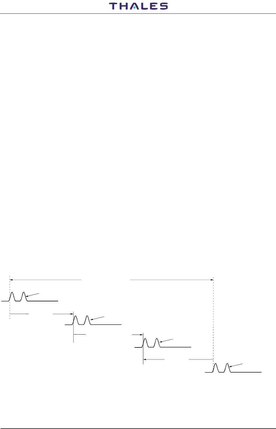
interrogating pulse pair and the transmission of the corresponding reply ( see Figure 1.1).
Travel time (50µs+1µs/150m)
Interrogation Paire pulses
transmitted by aircraft
One way time
1µs/300m
Replay Delay of the beacon
(50µs)
One way time
1µs/300m
Interrogation Paire pulses
received by transponder
Replay delay Paire pulses
transmitted by transponder
Replay Paire pulses
received by aircraft
Figure 1.1. DME - Principle of the RF signals path
The transponder periodically transmits special identification pulse groups, interleaved with the reply and
squitter pulses that can be decoded by the aircraft as a Morse tone, keyed with the beacon code name.
955 900 031C DME 415/435 -Technical Manual
Vol. 1-Section 1-General Information
1-2 THALES Italia S.p.A.- A. S. D. Vers. D, September 2005
The airborne receiver is able to recognize the replies to its own interrogations, among the many other pulses
transmitted by the beacon, by means of a stroboscopic procedure.
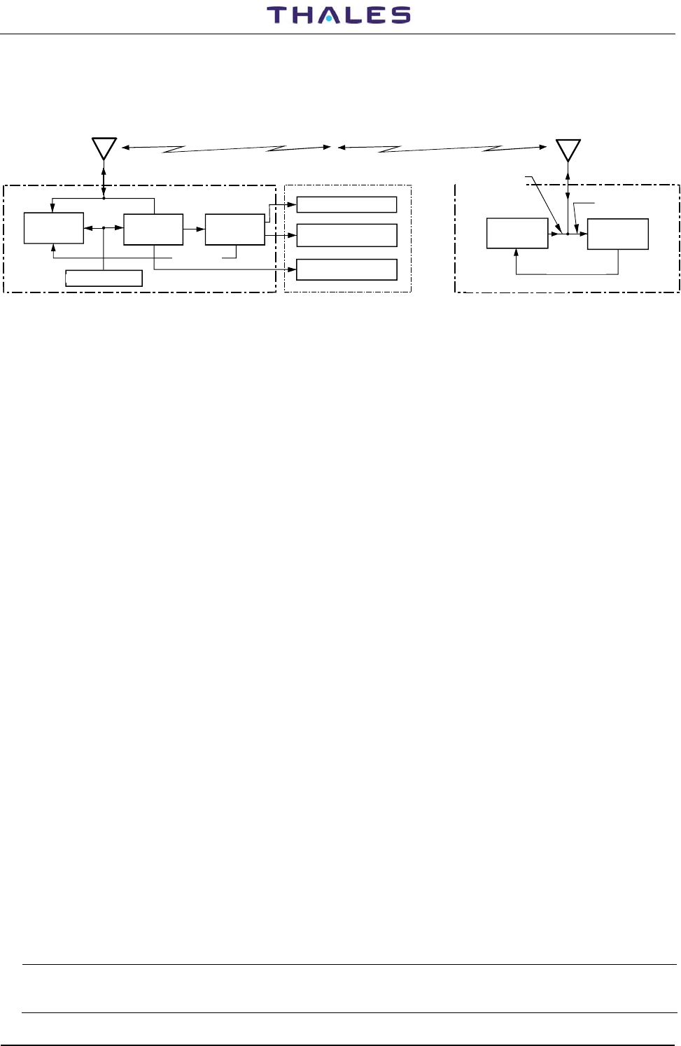
The DME theory of operation is summarized in a block diagram in Figure 1.2.
BEACON
IDENTIFICATION TONE
TRANSMITTER RECEIVER
AUTOPILOT
TRANSMITTER RECEIVER
DISTANCE
CIRCUITS
DME
AIRBORNE CHANNEL SELECTOR
DISTANCE INFORMATION
TO BOARD INDICATOR
AIRCRAFT'S
ANTENNA
DME GROUND BEACON
TRANSMITS DISTANCE
INFORMATION
and IDENTIFICATION
SIGNAL
REPLY TRIGGER TO
INTERROGATIONS
RECEIVED
INTERROGATIONS
BEACON'S
ANTENNA
INTERROGATION
TRIGGERS
Figure 1.2. DME - Theory of operation, simplified block diagram
1.2.1 Coverage
According to the frequency band used, the DME system coverage is limited to the optical range and
depends on the aircraft flight altitude and on the type of ground.
The high frequency used and the use of special techniques have made the system much less sensitive to
site errors than other types of omni-directional beacons now in use.
1.2.2 Traffic Capacity
The aircraft handling capacity is adequate for a traffic peak of 200 aircrafts. When the traffic peak exceeds
200 aircrafts the transponder should be capable of handling that peak.
1.2.3 Accuracy
As a result of the development and the applications of modern electronic technologies, the accuracy of the
distance information provided by the DME system is improving all the time.
At present, the accuracy of a DME system can be considered within the maximum values specified below:
±0.12 NM +0.05% of the distance, from 0 to 65 nautical miles, and ± 0.17 NM +0.05% of the distance, above
65 nautical miles.
1.2.4 Nominal Reply Delay – Pair Pulse Code - Channeling
Each beacon is identified by means of its channel frequency, its pulse coding and its identity signal.
The ground beacon introduces a fixed delay between the reception of interrogating pulses and the
transmission of the corresponding reply pulses.
This fixed delay, called main delay or fundamental delay, is introduced. So that an aircraft which is flying
very close to the beacon can complete transmission of the encoded interrogating pulse pair, and then
deactivate its own transmitter, before its receiver begins receiving the corresponding beacon reply pulses.
To render the system as immune as possible to errors caused by interfering signals, the DME system
transmits pulse pairs instead of single pulses; each pair includes two 3.5 µs pulses whose spacing depends
on the channel mode selected.
The channel code, pulse code, reply delay and operating mode are shown on the following table (standard
ICAO).
Channel
Code
Nominal
Interrogation Pulse Code
[µs]
Transponder
Reply Pulse Code
[µs]
Transponder
Nominal Reply Delay
[µs]
X 12 12.0 ± 0.1 50
Y 36 30.0 ± 0.1 56
DME 415/435 -Technical Manual
Vol. 1-Section 1-General Information 955 900 031C
Vers. D, September 2005 THALES Italia S.p.A.- A. S. D. 1-3
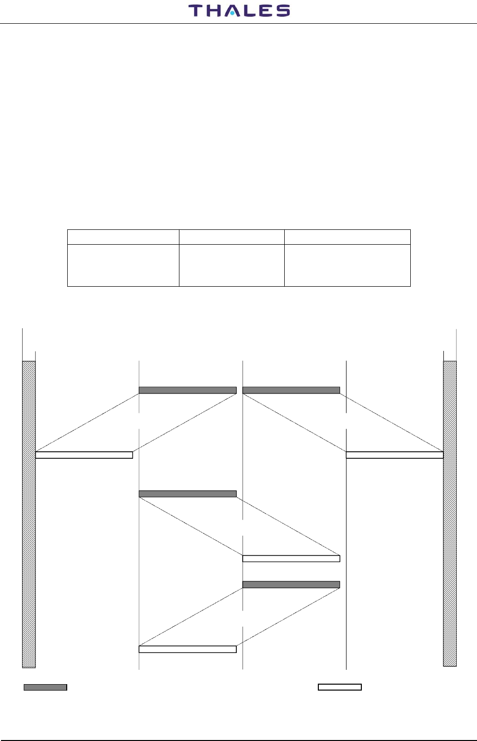
Each operational channel in the DME system is defined by two frequencies (interrogation and reply
frequencies), spaced 63 MHz apart, and by the pulse code for the assigned channel (X or Y channel).
The DME system transmits on a pre-selected channel among the 252 available ones. These channels are
divided into 126 X channels and 126 Y channels providing a frequency ranging from 1025 to 1150 MHz for
aircraft transmission (interrogation). Moreover, a 962 to 1213 MHz frequency for signal reception by the
aircraft (ground beacon reply transmission). Interrogation and reply frequencies are assigned with one MHz
spacing between channels.
The diagram shown in figure 1.3 gives the aircraft interrogation frequency associated to the beacon reply
frequency for both channel types X, Y. The same information is also given in table 1-1 and table 1-2 for X
and Y channels respectively, as per ICAO ANNEX 10.
Each beacon emits a Morse identity code signal that can be heard in the pilot headset; this code consists of
pulse pairs transmitted at a frequency of 1350 Hz.
Each beacon is therefore identified by means of its channel frequency, its pulse coding and its identity
signal.
Table 1-1. Frequencies for DME Channels
X Channels (n° 126) Channel Y Channels (n° 126)
I = 1025 + (CH-1) I = 1025 + (CH-1)
R = I - 63 1 ≤ CH ≤ 63 R = I + 63
R = I + 63 64 ≤ CH ≤ 126 R = I - 63
I = INTERROGATION FREQUENCY (MHz) CH = CHANNEL NUMBER
R = REPLY FREQUENCY (MHz)
960 MHz
962 MHz 1025 MHz 1213 MHz
1215 MHz
1-63X 64-126X
1-63Y
64-126Y
1088 MHz 1151 MHz
INTERROGATION FREQUENCIES REPLY FREQUENCIES
Figure 1.3. DME Channels Reply and Interrogation Frequencies

955 900 031C DME 415/435 -Technical Manual
Vol. 1-Section 1-General Information
1-4 THALES Italia S.p.A.- A. S. D. Vers. D, September 2005
Table 1-2. Frequencies and Code Pulses for DME Channels (1 to 17)
DME PARAMETERS
CHANNEL PAIRING INTERROGATION REPLY
Pulse Codes
DME/P
DME
Channel
VHF
FREQ.
MHz
MLS
FREQ.
MHz
MLS
Channel
Frequency
MHz
DME/N
µs
IAM
µs
FAM
µs
Frequency
MHz
Pulse
Codes
µs
1X
1Y
−
−
−
−
−
−
1025
1025
12
36
−
−
−
−
962
1088
12
30
2X
2Y
−
−
−
−
−
−
1026
1026
12
36
−
−
−
−
963
1089
12
30
3X
3Y
−
−
−
−
−
−
1027
1027
12
36
−
−
−
−
964
1090
12
30
4X
4Y
−
−
−
−
−
−
1028
1028
12
36
−
−
−
−
965
1091
12
30
5X
5Y
−
−
−
−
−
−
1029
1029
12
36
−
−
−
−
966
1092
12
30
6X
6Y
−
−
−
−
−
−
1030
1030
12
36
−
−
−
−
967
1093
12
30
7X
7Y
−
−
−
−
−
−
1031
1031
12
36
−
−
−
−
968
1094
12
30
8X
8Y
−
−
−
−
−
−
1032
1032
12
36
−
−
−
−
969
1095
12
30
9X
9Y
−
−
−
−
−
−
1033
1033
12
36
−
−
−
−
970
1096
12
30
10X
10Y
−
−
−
−
−
−
1034
1034
12
36
−
−
−
−
971
1097
12
30
11X
11Y
−
−
−
−
−
−
1035
1035
12
36
−
−
−
−
972
1098
12
30
12X
12Y
−
−
−
−
−
−
1036
1036
12
36
−
−
−
−
973
1099
12
30
13X
13Y
−
−
−
−
−
−
1037
1037
12
36
−
−
−
−
974
1100
12
30
14X
14Y
−
−
−
−
−
−
1038
1038
12
36
−
−
−
−
975
1101
12
30
15X
15Y
−
−
−
−
−
−
1039
1039
12
36
−
−
−
−
976
1102
12
30
16X
16Y
−
−
−
−
−
−
1040
1040
12
36
−
−
−
−
977
1103
12
30
17X
17Y
17Z
108.00
108.05
−
−
5043.0
5043.3
−
540
541
1041
1041
1041
12
36
−
−
36
21
−
42
27
978
1104
1104
12
30
15

DME 415/435 -Technical Manual
Vol. 1-Section 1-General Information 955 900 031C
Vers. D, September 2005 THALES Italia S.p.A.- A. S. D. 1-5
Table 1-2. Frequencies and Code Pulses for DME Channels (18 to 28)
DME PARAMETERS
CHANNEL PAIRING INTERROGATION REPLY
Pulse Codes
DME/P
DME
Channel
VHF
FREQ.
MHz
MLS
FREQ.
MHz
MLS
Channel
Frequency
MHz
DME/N
µs
IAM
µs
FAM
µs
Frequency
MHz
Pulse
Codes
µs
18X
18W
18Y
18Z
108.10
−
108.15
−
5031.0
5031.3
5043.6
5043.9
500
501
542
543
1042
1042
1042
1042
12
−
36
−
12
24
36
21
18
30
42
27
979
979
1105
1105
12
24
30
15
19X
19Y
19Z
108.20
108.25
−
−
5044.2
5044.5
−
544
545
1043
1043
1043
12
36
−
−
36
21
−
42
27
980
1106
1106
12
30
15
20X
20W
20Y
20Z
108.30
−
108.35
−
5031.6
5031.9
5044.8
5045.1
502
503
546
547
1044
1044
1044
1044
12
−
36
−
12
24
36
21
18
30
42
27
981
981
1107
1107
12
24
30
15
21X
21Y
21Z
108.40
108.45
−
−
5045.4
5045.7
−
548
549
1045
1045
1045
12
36
−
−
36
21
−
42
27
982
1108
1108
12
30
15
22X
22W
22Y
22Z
108.50
−
108.55
−
5032.2
5032.5
5046.0
5046.3
504
505
550
551
1046
1046
1046
1046
12
−
36
−
12
24
36
21
18
30
42
27
983
983
1109
1109
12
24
30
15
23X
23Y
23Z
108.60
108.65
−
−
5046.6
5046.9
−
552
553
1047
1047
1047
12
36
−
−
36
21
−
42
27
984
1110
1110
12
30
15
24X
24W
24Y
24Z
108.70
−
108.75
−
5032.8
5033.1
5047.2
5047.5
506
507
554
555
1048
1048
1048
1048
12
−
36
−
12
24
36
21
18
30
42
27
985
985
1111
1111
12
24
30
15
25X
25Y
25Z
108.80
108.85
−
−
5047.8
5048.1
−
556
557
1049
1049
1049
12
36
−
−
36
21
−
42
27
986
1112
1112
12
30
15
26X
26W
26Y
26Z
108.90
−
108.95
−
5033.4
5033.7
5048.4
5048.7
508
509
558
559
1050
1050
1050
1050
12
−
36
−
12
24
36
21
18
30
42
27
987
987
1113
1113
12
24
30
15
27X
27Y
27Z
109.00
109.05
−
−
5049.0
5049.3
−
560
561
1051
1051
1051
12
36
−
−
36
21
−
42
27
988
1114
1114
12
30
15
28X
28W
28Y
28Z
109.10
−
109.15
−
5034.0
5034.3
5049.6
5049.9
510
511
562
563
1052
1052
1052
1052
12
−
36
−
12
24
36
21
18
30
42
27
989
989
1115
1115
12
24
30
15

955 900 031C DME 415/435 -Technical Manual
Vol. 1-Section 1-General Information
1-6 THALES Italia S.p.A.- A. S. D. Vers. D, September 2005
Table 1-2. Frequencies and Code Pulses for DME Channels (29 to 40)
DME PARAMETERS
CHANNEL PAIRING INTERROGATION REPLY
Pulse Codes
DME/P
DME
Channel
VHF
FREQ.
MHz
MLS
FREQ.
MHz
MLS
Channel
Frequency
MHz
DME/N
µs
IAM
µs
FAM
µs
Frequency
MHz
Pulse
Codes
µs
29X
29Y
29Z
109.20
109.25
−
−
5050.2
5050.5
−
564
565
1053
1053
1053
12
36
−
−
36
21
−
42
27
990
1116
1116
12
30
15
30X
30W
30Y
30Z
109.30
−
109.35
−
5034.6
5034.9
5050.8
5051.1
512
513
566
567
1054
1054
1054
1054
12
−
36
−
12
24
36
21
18
30
42
27
991
991
1117
1117
12
24
30
15
31X
31Y
31Z
109.40
109.45
−
−
5051.4
5051.7
−
568
569
1055
1055
1055
12
36
−
−
36
21
−
42
27
992
1118
1118
12
30
15
32X
32W
32Y
32Z
109.50
−
109.55
−
5035.2
5035.5
5052.0
5052.3
514
515
570
571
1056
1056
1056
1056
12
−
36
−
12
24
36
21
18
30
42
27
993
993
1119
1119
12
24
30
15
33X
33Y
33Z
109.60
109.65
−
−
5052.6
5052.9
−
572
573
1057
1057
1057
12
36
−
−
36
21
−
42
27
994
1120
1120
12
30
15
34X
34W
34Y
34Z
109.70
−
109.75
−
5035.8
5036.1
5053.2
5053.5
516
517
574
575
1058
1058
1058
1058
12
−
36
−
12
24
36
21
18
30
42
27
995
995
1121
1121
12
24
30
15
35X
35Y
35Z
109.80
109.85
−
−
5053.8
5054.1
−
576
577
1059
1059
1059
12
36
−
−
36
21
−
42
27
996
1122
1122
12
30
15
36X
36W
36Y
36Z
109.90
−
109.95
−
5036.4
5036.7
5054.4
5054.7
518
519
578
579
1060
1060
1060
1060
12
−
36
−
12
24
36
21
18
30
42
27
997
997
1123
1123
12
24
30
15
37X
37Y
37Z
110.00
110.05
−
−
5055.0
5055.3
−
580
581
1061
1061
1061
12
36
−
−
36
21
−
42
27
998
1124
1124
12
30
15
38X
38W
38Y
38Z
110.10
−
110.15
−
5037.0
5037.3
5055.6
5055.9
520
521
582
583
1062
1062
1062
1062
12
−
36
−
12
24
36
21
18
30
42
27
999
999
1125
1125
12
24
30
15
39X
39Y
39Z
110.20
110.25
−
−
5056.2
5056.5
−
584
585
1063
1063
1063
12
36
−
−
36
21
−
42
27
1000
1126
1126
12
30
15
40X
40W
40Y
40Z
110.30
−
110.35
−
5037.6
5037.9
5056.8
5057.1
522
523
586
587
1064
1064
1064
1064
12
−
36
−
12
24
36
21
18
30
42
27
1001
1001
1127
1127
12
24
30
15

DME 415/435 -Technical Manual
Vol. 1-Section 1-General Information 955 900 031C
Vers. D, September 2005 THALES Italia S.p.A.- A. S. D. 1-7
Table 1-2. Frequencies and Code Pulses for DME Channels (41 to 52)
DME PARAMETERS
CHANNEL PAIRING INTERROGATION REPLY
Pulse Codes
DME/P
DME
Channel
VHF
FREQ.
MHz
MLS
FREQ.
MHz
MLS
Channel
Frequency
MHz
DME/N
µs
IAM
µs
FAM
µs
Frequency
MHz
Pulse
Codes
µs
41X
41Y
41Z
110.40
110.45
−
−
5057.4
5057.7
−
588
589
1065
1065
1065
12
36
−
−
36
21
−
42
27
1002
1128
1128
12
30
15
42X
42W
42Y
42Z
110.50
−
110.55
−
5038.2
5038.5
5058.0
5058.3
524
525
590
591
1066
1066
1066
1066
12
−
36
−
12
24
36
21
18
30
42
27
1003
1003
1129
1129
12
24
30
15
43X
43Y
43Z
110.60
110.65
−
−
5058.6
5058.9
−
592
593
1067
1067
1067
12
36
−
−
36
21
−
42
27
1004
1130
1130
12
30
15
44X
44W
44Y
44Z
110.70
−
110.75
−
5038.8
5039.1
5059.2
5059.5
526
527
594
595
1068
1068
1068
1068
12
−
36
−
12
24
36
21
18
30
42
27
1005
1005
1131
1131
12
24
30
15
45X
45Y
45Z
110.80
110.85
−
−
5059.8
5060.1
−
596
597
1069
1069
1069
12
36
−
−
36
21
−
42
27
1006
1132
1132
12
30
15
46X
46W
46Y
46Z
110.90
−
110.95
−
5039.4
5039.7
5060.4
5060.7
528
529
598
599
1070
1070
1070
1070
12
−
36
−
12
24
36
21
18
30
42
27
1007
1007
1133
1133
12
24
30
15
47X
47Y
47Z
111.00
111.05
−
−
5061.0
5061.3
−
600
601
1071
1071
1071
12
36
−
−
36
21
−
42
27
1008
1134
1134
12
30
15
48X
48W
48Y
48Z
111.10
−
111.15
−
5040.0
5040.3
5061.6
5061.9
530
531
602
603
1072
1072
1072
1072
12
−
36
−
12
24
36
21
18
30
42
27
1009
1009
1135
1135
12
24
30
15
49X
49Y
49Z
111.20
111.25
−
−
5062.2
5062.5
−
604
605
1073
1073
1073
12
36
−
−
36
21
−
42
27
1010
1136
1136
12
30
15
50X
50W
50Y
50Z
111.30
−
111.35
−
5040.6
5040.9
5062.8
5063.1
532
533
606
607
1074
1074
1074
1074
12
−
36
−
12
24
36
21
18
30
42
27
1011
1011
1137
1137
12
24
30
15
51X
51Y
51Z
111.40
111.45
−
−
5063.4
5063.7
−
608
609
1075
1075
1075
12
36
−
−
36
21
−
42
27
1012
1138
1138
12
30
15
52X
52W
52Y
52Z
111.50
−
111.55
−
5041.2
5041.5
5064.0
5064.3
534
535
610
611
1076
1076
1076
1076
12
−
36
−
12
24
36
21
18
30
42
27
1013
1013
1139
1139
12
24
30
15

955 900 031C DME 415/435 -Technical Manual
Vol. 1-Section 1-General Information
1-8 THALES Italia S.p.A.- A. S. D. Vers. D, September 2005
Table 1-2. Frequencies and Code Pulses for DME Channels (53 to 68)
DME PARAMETERS
CHANNEL PAIRING INTERROGATION REPLY
Pulse Codes
DME/P
DME
Channel
VHF
FREQ.
MHz
MLS
FREQ.
MHz
MLS
Channel
Frequency
MHz
DME/N
µs
IAM
µs
FAM
µs
Frequency
MHz
Pulse
Codes
µs
53X
53Y
53Z
111.60
111.65
−
−
5064.5
5064.9
−
612
613
1077
1077
1077
12
36
−
−
36
21
−
42
27
1014
1140
1140
12
30
15
54X
54W
54Y
54Z
111.70
−
111.75
−
5041.8
5042.1
5065.2
5065.5
536
537
614
615
1078
1078
1078
1078
12
−
36
−
12
24
36
21
18
30
42
27
1015
1015
1141
1141
12
24
30
15
55X
55Y
55Z
111.80
111.85
−
−
5065.8
5066.1
−
616
617
1079
1079
1079
12
36
−
−
36
21
−
42
27
1016
1142
1142
12
30
15
56X
56W
56Y
56Z
111.90
−
111.95
−
5042.4
5042.7
5066.4
5066.7
538
539
618
619
1080
1080
1080
1080
12
−
36
−
12
24
36
21
18
30
42
27
1017
1017
1143
1143
12
24
30
15
57X
57Y
112.00
112.05
−
−
−
−
1081
1081
12
36
−
−
−
−
1018
1144
12
30
58X
58Y
112.10
112.15
−
−
−
−
1082
1082
12
36
−
−
−
−
1019
1145
12
30
59X
59Y
112.20
112.25
−
−
−
−
1083
1083
12
36
−
−
−
−
1020
1146
12
30
60X
60Y
−
−
−
−
−
−
1084
1084
12
36
−
−
−
−
1021
1147
12
30
61X
61Y
−
−
−
−
−
−
1085
1085
12
36
−
−
−
−
1022
1148
12
30
62X
62Y
−
−
−
−
−
−
1086
1086
12
36
−
−
−
−
1023
1149
12
30
63X
63Y
−
−
−
−
−
−
1087
1087
12
36
−
−
−
−
1024
1150
12
30
64X
64Y
−
−
−
−
−
−
1088
1088
12
36
−
−
−
−
1151
1025
12
30
65X
65Y
−
−
−
−
−
−
1089
1089
12
36
−
−
−
−
1152
1026
12
30
66X
66Y
−
−
−
−
−
−
1090
1090
12
36
−
−
−
−
1153
1027
12
30
67X
67Y
−
−
−
−
−
−
1091
1091
12
36
−
−
−
−
1154
1028
12
30
68X
68Y
−
−
−
−
−
−
1092
1092
12
36
−
−
−
−
1155
1029
12
30

DME 415/435 -Technical Manual
Vol. 1-Section 1-General Information 955 900 031C
Vers. D, September 2005 THALES Italia S.p.A.- A. S. D. 1-9
Table 1-2. Frequencies and Code Pulses for DME Channels (69 to 85)
DME PARAMETERS
CHANNEL PAIRING INTERROGATION REPLY
Pulse Codes
DME/P
DME
Channel
VHF
FREQ.
MHz
MLS
FREQ.
MHz
MLS
Channel
Frequency
MHz
DME/N
µs
IAM
µs
FAM
µs
Frequency
MHz
Pulse
Codes
µs
69X
69Y
−
−
−
−
−
−
1093
1093
12
36
−
−
−
−
1156
1030
12
30
70X
70Y
112.30
112.35
−
−
−
−
1094
1094
12
36
−
−
−
−
1157
1031
12
30
71X
71Y
112.40
112.45
−
−
−
−
1095
1095
12
36
−
−
−
−
1158
1032
12
30
72X
72Y
112.50
112.55
−
−
−
−
1096
1096
12
36
−
−
−
−
1159
1033
12
30
73X
73Y
112.60
112.65
−
−
−
−
1097
1097
12
36
−
−
−
−
1160
1034
12
30
74X
74Y
112.70
112.75
−
−
−
−
1098
1098
12
36
−
−
−
−
1161
1035
12
30
75X
75Y
112.80
112.85
−
−
−
−
1099
1099
12
36
−
−
−
−
1162
1036
12
30
76X
76Y
112.90
112.95
−
−
−
−
1100
1100
12
36
−
−
−
−
1163
1037
12
30
77X
77Y
113.00
113.05
−
−
−
−
1101
1101
12
36
−
−
−
−
1164
1038
12
30
78Y
78Y
113.10
113.15
−
−
−
−
1102
1102
12
36
−
−
−
−
1165
1039
12
30
79X
79Y
113.20
113.25
−
−
−
−
1103
1103
12
36
−
−
−
−
1166
1040
12
30
80X
80Y
80Z
113.30
113.35
−
−
5067.0
5067.3
−
620
621
1104
1104
1104
12
36
−
−
36
21
−
42
27
1167
1041
1041
12
30
15
81X
81Y
81Z
113.40
113.45
−
−
5067.6
5067.9
−
622
623
1105
1105
1105
12
36
−
−
36
21
−
42
27
1168
1042
1042
12
30
15
82X
82Y
82Z
113.50
113.55
−
−
5068.2
5068.5
−
624
625
1106
1106
1106
12
36
−
−
36
21
−
42
27
1169
1043
1043
12
30
15
83X
83Y
83Z
113.60
113.65
−
−
5068.8
5069.1
−
626
627
1107
1107
1107
12
36
−
−
36
21
−
42
27
1170
1044
1044
12
30
15
84X
84Y
84Z
113.70
113.75
−
−
5069.4
5069.7
−
628
629
1108
1108
1108
12
36
−
−
36
21
−
42
27
1171
1045
1045
12
30
15
85X
85Y
85Z
113,80
113,85
-
5070.0
5071.3
1109
1109
1109
12
36
-
-
36
21
-
42
27
1172
1046
1046
12
30
15

955 900 031C DME 415/435 -Technical Manual
Vol. 1-Section 1-General Information
1-10 THALES Italia S.p.A.- A. S. D. Vers. D, September 2005
Table 1-2. Frequencies and Code Pulses for DME Channels (86 to 99)
DME PARAMETERS
CHANNEL PAIRING INTERROGATION REPLY
Pulse Codes
DME/P
DME
Channel
VHF
FREQ.
MHz
MLS
FREQ.
MHz
MLS
Channel
Frequency
MHz
DME/N
µs
IAM
µs
FAM
µs
Frequency
MHz
Pulse
Codes
µs
86X
86Y
86Z
113.90
113.95
−
−
5070.6
5070.9
−
632
633
1110
1110
1110
12
36
−
−
36
21
−
42
27
1173
1047
1047
12
30
15
87X
87Y
87Z
114.00
114.05
−
−
5071.2
5071.5
−
634
635
1111
1111
1111
12
36
−
−
36
21
−
42
27
1174
1048
1048
12
30
15
88X
88Y
88Z
114.10
114.15
−
−
5071.8
5072.1
−
636
637
1112
1112
1112
12
36
−
−
36
21
−
42
27
1175
1049
1049
12
30
15
89X
89Y
89Z
114.20
114.25
−
−
5072.4
5072.7
−
638
639
1113
1113
1113
12
36
−
−
36
21
−
42
27
1176
1050
1050
12
30
15
90X
90Y
90Z
114.30
114.35
−
−
5073.0
5073.3
−
640
641
1114
1114
1114
12
36
−
−
36
21
−
42
27
1177
1051
1051
12
30
15
91X
91Y
91Z
114.40
114.45
−
−
5073.6
5073.9
−
642
643
1115
1115
1115
12
36
−
−
36
21
−
42
27
1178
1052
1052
12
30
15
92X
92Y
92Z
114.50
114.55
−
−
5074.2
5074.5
−
644
645
1116
1116
1116
12
36
−
−
36
21
−
42
27
1179
1053
1053
12
30
15
93X
93Y
93Z
114.60
114.65
−
−
5074.8
5075.1
−
646
647
1117
1117
1117
12
36
−
−
36
21
−
42
27
1180
1054
1054
12
30
15
94X
94Y
94Z
114.70
114.75
−
−
5075.4
5075.7
−
648
649
1118
1118
1118
12
36
−
−
36
21
−
42
27
1181
1055
1055
12
30
15
95X
95Y
95Z
114.80
114.85
−
−
5076.0
5076.3
−
650
651
1119
1119
1119
12
36
−
−
36
21
−
42
27
1182
1056
1056
12
30
15
96X
96Y
96Z
114.90
114.95
−
−
5076.6
5076.9
−
652
653
1120
1120
1120
12
36
−
−
36
21
−
42
27
1183
1057
1057
12
30
15
97X
97Y
97Z
115.00
115.05
−
−
5077.2
5077.5
−
654
655
1121
1121
1121
12
36
−
−
36
21
−
42
27
1184
1058
1058
12
30
15
98X
98Y
98Z
115.10
115.15
−
−
5077.8
5078.1
−
656
657
1122
1122
1122
12
36
−
−
36
21
−
42
27
1185
1059
1059
12
30
15
99X
99Y
99Z
115.20
115.25
−
−
5078.4
5078.7
−
658
659
1123
1123
1123
12
36
−
−
36
21
−
42
27
1186
1060
1060
12
30
15

DME 415/435 -Technical Manual
Vol. 1-Section 1-General Information 955 900 031C
Vers. D, September 2005 THALES Italia S.p.A.- A. S. D. 1-11
Table 1-2. Frequencies and Code Pulses for DME Channels (100 to 113)
DME PARAMETERS
CHANNEL PAIRING INTERROGATION REPLY
Pulse Codes
DME/P
DME
Channel
VHF
FREQ.
MHz
MLS
FREQ.
MHz
MLS
Channel
Frequency
MHz
DME/N
µs
IAM
µs
FAM
µs
Frequency
MHz
Pulse
Codes
µs
100X
100Y
100Z
115.30
115.35
−
−
5079.0
5079.3
−
660
661
1124
1124
1124
12
36
−
−
36
21
−
42
27
1187
1061
1061
12
30
15
101X
101Y
101Z
115.40
115.45
−
−
5079.6
5079.9
−
662
663
1125
1125
1125
12
36
−
−
36
21
−
42
27
1188
1062
1062
12
30
15
102X
102Y
102Z
115.50
115.55
−
−
5080.2
5080.5
−
664
665
1126
1126
1126
12
36
−
−
36
21
−
42
27
1189
1063
1063
12
30
15
103X
103Y
103Z
115.60
115.65
−
−
5080.8
5081.1
−
666
667
1127
1127
1127
12
36
−
−
36
21
−
42
27
1190
1064
1064
12
30
15
104X
104Y
104Z
115.70
115.75
−
−
5081.4
5081.7
−
668
669
1128
1128
1128
12
36
−
−
36
21
−
42
27
1191
1065
1065
12
30
15
105X
105Y
105Z
115.80
115.85
−
−
5082.0
5082.3
−
670
671
1129
1129
1129
12
36
−
−
36
21
−
42
27
1192
1066
1066
12
30
15
106X
106Y
106Z
115.90
115.95
−
−
5082.6
5082.9
−
672
673
1130
1130
1130
12
36
−
−
36
21
−
42
27
1193
1067
1067
12
30
15
107X
107Y
107Z
116.00
116.05
−
−
5083.2
5083.5
−
674
675
1131
1131
1131
12
36
−
−
36
21
−
42
27
1194
1068
1068
12
30
15
108X
108Y
108Z
116.10
116.15
−
−
5083.8
5084.1
−
676
677
1132
1132
1132
12
36
−
−
36
21
−
42
27
1195
1069
1069
12
30
15
109X
109Y
109Z
116.20
116.25
−
−
5084.4
5084.7
−
678
679
1133
1133
1133
12
36
−
−
36
21
−
42
27
1196
1070
1070
12
30
15
110X
110Y
110Z
116.30
116.35
−
−
5085.0
5085.3
−
680
681
1134
1134
1134
12
36
−
−
36
21
−
42
27
1197
1071
1071
12
30
15
111X
111Y
111Z
116.40
116.45
−
−
5085.6
5085.9
−
682
683
1135
1135
1135
12
36
−
−
36
21
−
42
27
1198
1072
1072
12
30
15
112X
112Y
112Z
116.50
116.55
−
−
5086.2
5086.5
−
684
685
1136
1136
1136
12
36
−
−
36
21
−
42
27
1199
1073
1073
12
30
15
113X
113Y
113Z
116.60
116.65
−
−
5086.8
5087.1
−
686
687
1137
1137
1137
12
36
−
−
36
21
−
42
27
1200
1074
1074
12
30
15

955 900 031C DME 415/435 -Technical Manual
Vol. 1-Section 1-General Information
1-12 THALES Italia S.p.A.- A. S. D. Vers. D, September 2005
Table 1-2. Frequencies and Code Pulses for DME Channels (114 to 126)
DME PARAMETERS
CHANNEL PAIRING INTERROGATION REPLY
Pulse Codes
DME/P
DME
Channel
VHF
FREQ.
MHz
MLS
FREQ.
MHz
MLS
Channel
Frequency
MHz
DME/N
µs
IAM
µs
FAM
µs
Frequency
MHz
Pulse
Codes
µs
114X
114Y
114Z
116.70
116.75
−
−
5087.4
5087.7
−
688
689
1138
1138
1138
12
36
−
−
36
21
−
42
27
1201
1075
1075
12
30
15
115X
115Y
115Z
116.80
116.85
−
−
5088.0
5088.3
−
690
691
1139
1139
1139
12
36
−
−
36
21
−
42
27
1202
1076
1076
12
30
15
116X
116Y
116Z
116.90
116.95
−
−
5088.6
5088.9
−
692
693
1140
1140
1140
12
36
−
−
36
21
−
42
27
1203
1077
1077
12
30
15
117X
117Y
117Z
117.00
117.05
−
−
5089.2
5089.5
−
694
695
1141
1141
1141
12
36
−
−
36
21
−
42
27
1204
1078
1078
12
30
15
118X
118Y
118Z
117.10
117.15
−
−
5089.8
5090.1
−
696
697
1142
1142
1142
12
36
−
−
36
21
−
42
27
1205
1079
1079
12
30
15
119X
119Y
119Z
117.20
117.25
−
−
5090.4
5090.7
−
698
699
1143
1143
1143
12
36
−
−
36
21
−
42
27
1206
1080
1080
12
30
15
120X
120Y
117.30
117.35
−
−
−
−
1144
1144
12
36
−
−
−
−
1207
1081
12
30
121X
121Y
117.40
117.45
−
−
−
−
1145
1145
12
36
−
−
−
−
1208
1082
12
30
122X
122Y
117.50
117.55
−
−
−
−
1146
1146
12
36
−
−
−
−
1209
1083
12
30
123X
123Y
117.60
117.65
−
−
−
−
1147
1147
12
36
−
−
−
−
1210
1084
12
30
124X
124Y
117.70
117.75
−
−
−
−
1148
1148
12
36
−
−
−
−
1211
1085
12
30
125X
125Y
117.80
117.85
−
−
−
−
1149
1149
12
36
−
−
−
−
1212
1086
12
30
126X
126Y
117.90
117.95
−
−
−
−
1150
1150
12
36
−
−
−
−
1213
1087
12
30

DME 415/435 -Technical Manual
Vol. 1-Section 1-General Information 955 900 031C
Vers. D, September 2005 THALES Italia S.p.A.- A. S. D. 1-13
1.3 GENERAL FEATURES OF THE EQUIPMENT
1.3.1 Equipment Versions
The DME 415 and 435 are respectively the lower power and the higher power versions of a complete
family of latest-generation equipment composed by:
- Approach DME 415: a 100 W solid-state DME can be installed also in co-location with ILS
- En-route DME 435: a 1 kW solid-state DME can be installed also in co-location with VOR or DVOR.
The two versions all feature a high commonality of modules and of principles of operation.
1.3.2 Main Feature of the Equipment
The main features of the equipment are:
• Compliant with the ICAO specifications in Annex 10, 5th ed. and Eurocae MPS Ed. 57, standard 1 as
applicable.
• Compliant with EEC Directives for CE Marking (EMC and Safety)
• Housed in a single 19" cabinet
• Powerable both from mains and standard 48 V batteries, with a built-in battery charger as an option
• Fully dualized, (being composed of two transponders and two monitoring systems ) but configurable
also in the following versions:
1) single TRX and single Monitor
2) single TRX and dual Monitor
• Completely modular
• Accurate distance information: up to ±15 m
• Digitally controlled output pulse shape
• Microprocessor-controlled monitors and transponders
• Monitor-independent reply delay self-adjustment
• Automatically performed self-check and measurements, the results of which can be continuously
displayed
• Automatically provided ICAO performance checks at programmable intervals and results
storing/displaying/printing
• Capable of executing a resident diagnostic program to help the operator in fault location.
• Operable as a stand-alone unit, but conceived to be co-located with other navaids like ILS,VOR or
DVOR
• Control by a Personal Computer (PC) at beacon site, which can be duplicated at remote site; the PC
can also be a portable unit to be connected only when required for maintenance reasons
• Remote control is fully compatible with all the system 400 equipment and with previous versions of
DME’s (FSD-40/45)
• Able to be connected to both an RCSU-2040 (part of Thales: Remote Maintenance and Monitoring
Configuration - RMMC) and the FRCM/NS Remote Control and Monitoring Network System, or new
remote control MCS (Monitoring and Control System): highly versatile systems for interfacing and
controlling different navaids facilities.

955 900 031C DME 415/435 -Technical Manual
Vol. 1-Section 1-General Information
1-14 THALES Italia S.p.A.- A. S. D. Vers. D, September 2005
1.3.2.1 Engineering
• Accessibility: front door access is only required. Equipment can be wall-mounted.
• Modularity: all circuits are divided into functional modules.
• Interconnections: extensive use is made of printed board back panels, flat ribbon cables and semi-rigid
coaxial cables.
• Identifications: all modules are easily recognizable by P/N and a two/three/four-letter code (e.g.: RX,
TX, DPR, BCPS) permanently marked on easily readable surfaces. All modules, cables and connectors
are marked and keyed to prevent incorrect connection.
• Cooling: no blowers are required to remove heat from the equipment. Use is made of extruded
aluminum heat sinks.
• Printed boards: two - or multilayer printed boards with plated-through holes are used throughout the
equipment. High frequency circuits are implemented in microstrip technique.
• RF shielding: all RF circuits are accurately shielded in casting boxes.
• Components: only high-quality components are used, in order to meet the reliability requirements.
• Corrosion: protection against corrosion and fungus is obtained by means of suitable materials, finishes
and coatings.
1.3.2.2 Safety
• The equipment is designed to be intrinsically safe for the user. No dangerous voltages except mains are
used.
• All modules or places, where a dangerous voltage may be accessible, are firmly protected by covers not
removable without using tools and are clearly marked with warning readouts.
• Special protective circuits are built-in in order to ensure that any failure in the equipment does not cause
further damage to other parts or components.
1.3.2.3 Installation
• Installation of DME 415-435 requires preparation of the site (i.e. shelter or equipment room, antenna
support mast, cable layout, power and ground connections etc.- (see section 2 "INSTALLATION" and
ANNEX A "DME ANTENNA SITING CRITERIA" in this manual).
• Installation of the equipment is simple and can be accomplished in few hours even by unskilled personnel
with a minimum of tools. The equipment only requires a minimum of shelter room.
• Ground and flight tests may be performed with the assistance of Thales technicians if requested.
1.3.2.4 Operation
• The Operator's interface consists of a PC terminal connected to the equipment. The basic control of the
equipment (on/off or changeover) is possible with local I/O front panel, however, even when the PC is not
available,
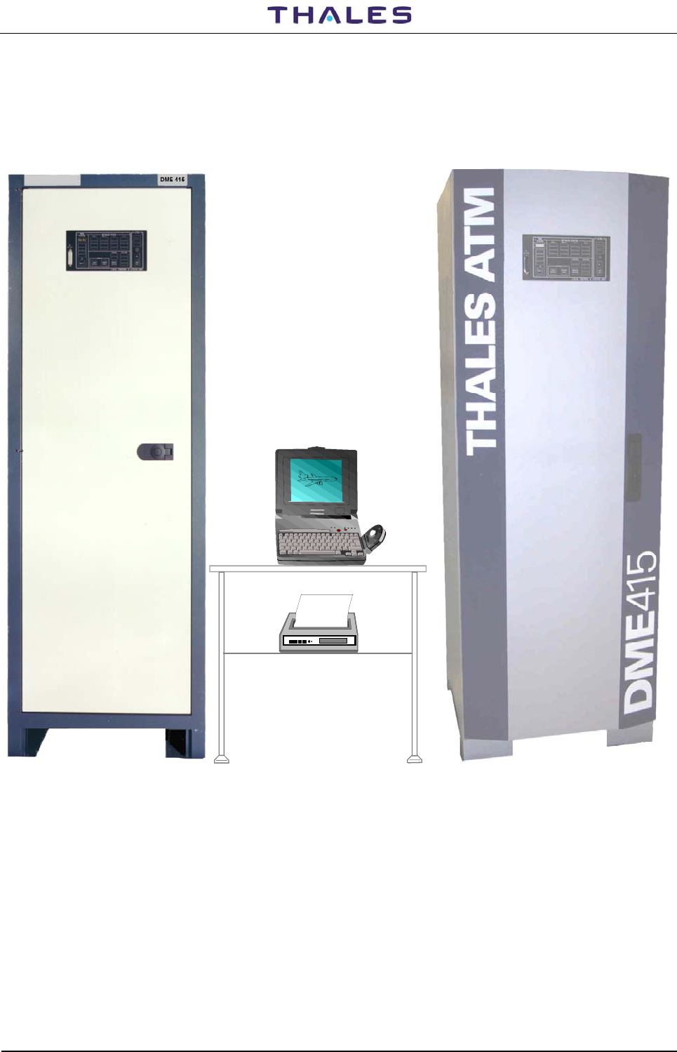
DME 415/435 -Technical Manual
Vol. 1-Section 1-General Information 955 900 031C
Vers. D, September 2005 THALES Italia S.p.A.- A. S. D. 1-15
Cabinet Part Number: 297.509.004 Cabinet Part Number: 297.509.007
Figure 1.4. DME 415 (same as DME 435) – Cabinet and PC, example of arrangement

955 900 031C DME 415/435 -Technical Manual
Vol. 1-Section 1-General Information
1-16 THALES Italia S.p.A.- A. S. D. Vers. D, September 2005
1.4 BEACON COMPOSITION AND IDENTIFICATION
The DME 415/435 ground equipment, as shown in figure 1.4, is constructed by THALES Italia S.p.A Air
Systems Division - Milan - Italy.
The DME versions are mounted in two cabinet’s types shown in figure 1.4 to customer choice.
The related reference modules labels of the equipment DME415/435 are given in table 1-3.
Table 1-3. Composition of the Equipment
Dual Single Name Ref.
Q.ty Label
1 1 Wired Cabinet (standard)
RF Path
2 1 Duplexer DPX
1 1 RF COAX Relay and PBA KCX
1 Coax Dummy Load -100 W, 50 Ω
1 1 External Filter Antenna KIT (optional)
2+2 1+1 10 dB + 10 dB PAD ( only for DME 435)
Interface System
1 1 Associated Facility Interface AFI
1 - Dummy Interface TAI
1 1 Modem 1 Party Line (LGM 1200) (option) MDM
1 1 Modem 2 LGM 28,8 D1 (option) MDM
Transponder and Monitor
2 1
Power Supply (DC/DC converter; + 5V, ± 15V ) PWS
2 1 Monitor MON
2 1 Receiver RX
2 1 Digital Processor DPR
2 1 Digital Modulator DMD
2 1 Transmitter 100 Wp (also driver for DME 435) TX 100
2 1 Transmitter Amplifier 1kWp (only for DME 435) TKW
Local I/O
1 1 Local Control Status Unit composed of:
- Control and Status Board
- Indication and Controls
LCSU
CSB
INC
Power Supply
1 1 Battery Charger and Power Supply subrack (option) BCPS
2 1 AC/DC 600W Module (option) AC-DC
1 1 Terminal bar- 48Vdc (option) -
1 1 Batteries supervisor only for BCPS Frako (option) -

DME 415/435 -Technical Manual
Vol. 1-Section 1-General Information 955 900 031C
Vers. D, September 2005 THALES Italia S.p.A.- A. S. D. 1-17
Table 1-4 gives the composition of the user interface for the local and remote sites.
The accompanying material supplied with the beacon is listed in table 1-5.
Table 1-4. User Interface Composition (option)
Q.TY NAME REF.
LOCAL SITE:
1 PC Requirements- Lap/Palm top
Processor Pentium 90 or better, (for use with MCS monitoring:
INTELP4, AMDK7 - Clock speed 2 GHz or better )
Operating system IBM/AT compatible suited to run 95, 98, 2000XP or
NT version (for MCS: WIN/NT, W2K, Linux)
Main memory 16 MB RAM min. (256/512 MB min for MCS)
VGA adapter color display: 32MB
HDD: 120 MB min. Hard Disk, min. 20MB free space on HDD
( 20GB/2x20GB min for MCS)
3.5” Floppy Disk FDD (1.44 MB),
CDROM drive,
Control via mouse or comparable
Serial interface connectors
-
1 Printer -
1 Status Indicator (repeater of the main indication beacon status) SI 446
REMOTE SITE:
1 Remote Control Status Indicator (composition: see RCSI or RCSE or MCS
technical manual)
RCSI 446
1 PC Requirements- Lap/Palm top: as Local site -
1 Keyboard (PC desk version) -
1 Printer -
1 Status Indicator (repeater of the main indication beacon status) SI 446
955 900 031C DME 415/435 -Technical Manual
Vol. 1-Section 1-General Information
1-18 THALES Italia S.p.A.- A. S. D. Vers. D, September 2005
Table 1-5. Material Supplied
Name NOTE
STANDARD
PC interconnection cable
OPTIONAL
Mains Cable
Grounding Cable
Battery Cable (+)
Battery Cable (-)
Auxiliary INPUT Cable (Parallel I/O)
Auxiliary OUTPUT Cable (Parallel I/O)
Cable for external modem
Interface Facility Cable (for AFI interface
module)
Serial data Cable (D-VOR/ILS)
Telephone Cable
Antenna coax cable
Antenna monitors probe coax cables
Obstruction light cable
Modem adapter Kit
Tool bag
Extender board - Video Digital (see Vol. 2
Section 1)
Extender board - RF (see Vol. 2 Section 1)
Figure 1.4 is a typical example of arrangement of the equipment and shows the front of a door. The local
indication and control panel is flush-mounted in the front door. It contains an RS232 connector for
interfacing with an intelligent terminal (PC).
Figures from 1.5 to 1.9 show the location of the parts and modules of the equipment valid for both cabinet
type.
Figure 1.8 shows the photos of DME 435 with front door closed and rear of equipment.
Each equipment module and part code number is indicated on Vol. 2: List of Components in this Technical
Manual.

DME 415/435 -Technical Manual
Vol. 1-Section 1-General Information 955 900 031C
Vers. D, September 2005 THALES Italia S.p.A.- A. S. D. 1-19
1.5 PHYSICAL AND MECHANICAL General Description
The standard (full dual) configuration of the DME 415-435 equipment is composed of two transponders, a
dual monitor system a RF path system, a Panel Control and a coaxial transfer relay unit. The parts of the
equipment are housed in a single 19" standard cabinet (cabinet’s types: view in fig. 1.4).
The cabinet, which is made of molded and welded steel sheet, can accommodate four 19” assembled
carriers (subracks). Plug-in units are used as double or single Euroform printed circuit boards, with
dimensions of 233.4 x 220 [mm] or 100 x 220 [mm].
The cabinet, which has a perforated metal plate on top and bottom, is self-ventilated (no forced ventilation
necessary).
NOTE: Do not block or seal the holes for the cooling air supply.
The front part of the cabinet is protected by a hinged door complete of locking mechanism and the Control
front Panel (Local I/O).
The top end of the cabinet provides four threaded holes used to screw in the eyebolts when the beacon is to
be lifted.
The RF output connector to the antenna and the RF antenna monitor input connectors are located on top of
the cabinet. The RF Duplexer modules are mounted inside of the "RF Amplifier/DPX" subrack on the upper
part of the cabinet. The 1 kWp RF amplifier modules are mounted on the lateral sides of the same subrack,
while the interface connections (e.g. modem, Associated Facility) are located on the bottom.
The RF components of the modules are in shielded casting boxes.
The Transponder/Monitor 1 and 2 subracks are located in middle part of the cabinet.
The AC/DC power supply units are located on the bottom of the cabinet. The BCPS subrack (optional)
comprises a terminal bar for mains and 48Vdc input.
Local I/O components (LCSU consisting of CSB module and INC module) are fastened to the hinged front
door in the upper part. The CSB board of the LCSU unit, combined with the INC module, is mounted on the
rear of the front door.
The local control front panel of the INC module part of LCSU unit is equipped with indicators and
commands:
− the indicators, for immediate check of beacon functioning and
− the main commands, for beacon control (acquisition and release of control, powering on/off,
transponder change over) without having to use the local PC.
The I/O panel with the external interconnection connectors is located in the top end of the cabinet (figure
1.9)
The front view of the DME 415 and DME 435 equipments, with the open door, is shown in figures 1.5 and
1.6. These figures show the positions of all the modules, which compose the equipment in the typical full (or
dual) version.
For special purposes, the equipment can be supplied in a single, non-redundant version, where very high
system availability is not mandatory.
Figure 1.7 shows the typical single version of the DME 435 equipment. The single version of the DME 415 is
the same as the DME 435 in which the final RF amplifier "TKW" module is removed.
The DME 415-435, dual or full version, is composed of a wired cabinet housing the following hardware parts
and modules:
Local I/O
• Local Control and Status Unit (LCSU) composed of
− Control Status Board module (CSB)
− Indication and Control module (INC)
• I/O Panel (on top of the cabinet)

955 900 031C DME 415/435 -Technical Manual
Vol. 1-Section 1-General Information
1-20 THALES Italia S.p.A.- A. S. D. Vers. D, September 2005
RF Amplifier/DPX subrack unit consisting of:
• Final Amplifier module (DME 435 only) (TKW)
• Duplexer module (DPX)
• Coaxial Relay and driver PBA (KCX and KCXM)
• Coax Dummy Load
• Association Facility Interface module (AFI)
• Interface (TAI dummy)
• Modem modules (optional) (MDM) ( including adapter kit : RS232 to TTL converter)
• Backpanel of the TKW (BPKW)
Transponder/Monitor 1 and 2 subrack units, both consisting of:
• DC/DC Power Supply module (PWS)
• Monitor/Interrogator module (MON)
• Receiver module (RX)
• Processor module (DPR)
• Modulator module (DMD)
• Transmitter (driver for DME 435) (TX100)
• Backpanel of the transponder/monitor (BPT)
Mains Power unit
• Battery Charger Power Supply subrack (BCPS)
• AC/DC module (AC/DC)
• Terminal Bar
All check and maintenance operations can be performed on the front of the equipment, upon opening the
cabinet front door.
Each subrack can be pulled out after unscrewing the fixing bolts (sliding are not provided).
All main modules (except the front ones of the LCSU unit) are plug-in types. Each module slides can be
easily pulled out by using proper handles placed on the front.
The bottom of the cabinet provides the entrance of the mains and 48 V dc cables through bush fair-leads
(see Section 2: INSTALLATION).
Connectors of the I/O panel mounted on the upper side of the cabinet provide the connection with the
external interface cables.
Each subrack has a backpanel on which connectors of the plug-in modules and the subrack interconnection
are mounted. All cable connectors (signals and mains) of subrack interconnection are within reach from the
front.
Interconnection with backpanels is provided by flat ribbon cables for low level signals and by cables for
48Vdc supply. Cables lay on the inside of the cabinet behind the subracks.
A 4-way (transfer type) RF coaxial relay is mounted on a support fixed on the upper side of the cabinet by
means of bolts (Figure 1.9), which can be unscrewed before inspecting the relay. The relay RF output is
directly connected to the antenna connector. The relay is power supplied through a specific interface circuit
fixed on the same coaxial relay.
The RF connection semi-rigid coaxial cables lay on the inside of the cabinet behind the subracks.
The semi-rigid coaxial cables end with floating coaxial connectors used for the sliding modules that also
comprise the RF circuits. The floating coaxial connectors are mounted on a reinforcement metal plate fixed
on the back of the back panels.
The coaxial cables used for the output RF power provide the minimum distance and end with type "N"
coaxial connectors.
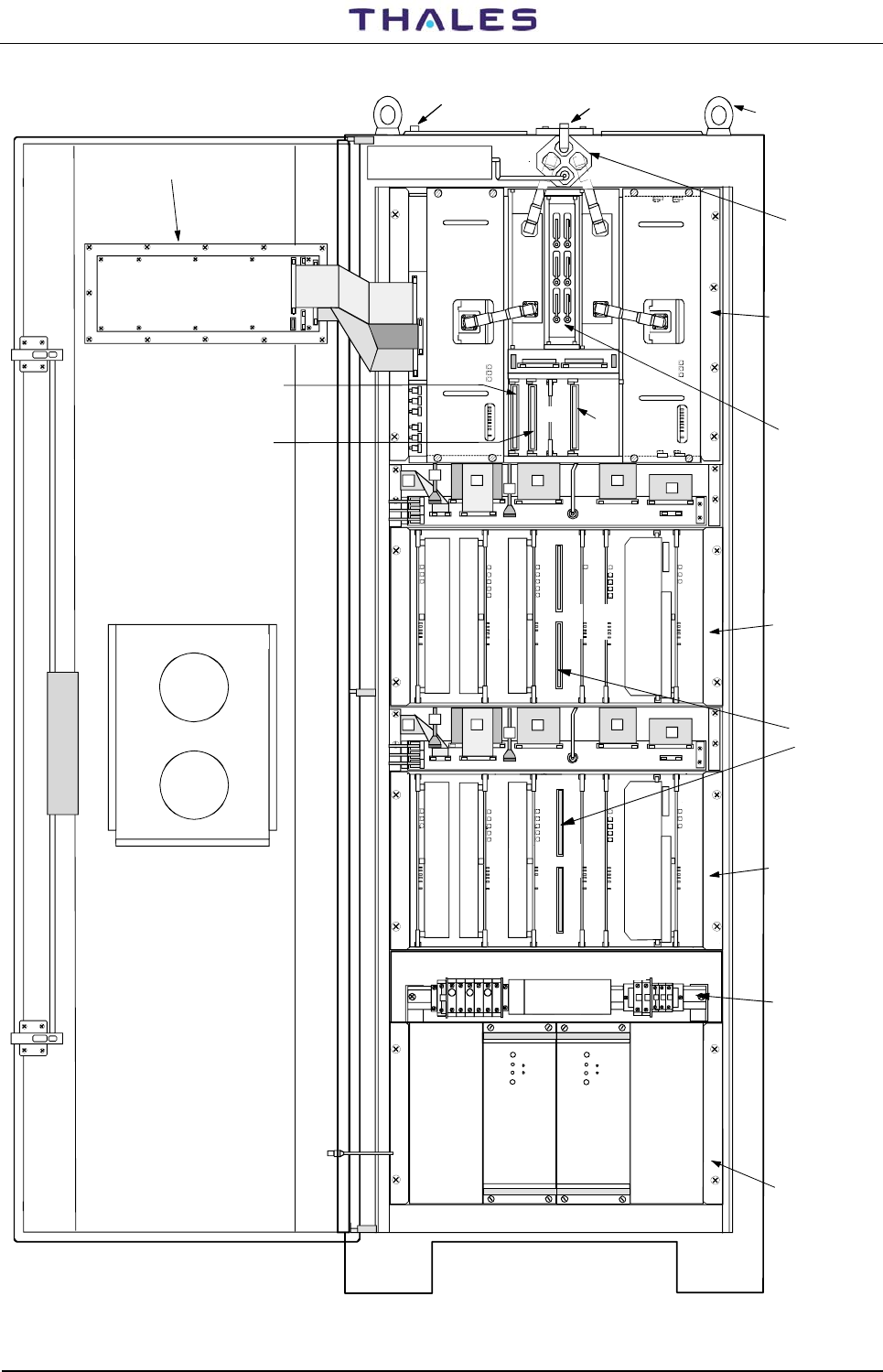
DME 415/435 -Technical Manual
Vol. 1-Section 1-General Information 955 900 031C
Vers. D, September 2005 THALES Italia S.p.A.- A. S. D. 1-21
DH
B
C
E
J1
F
DH
B
C
E
J1
F
AFI
TX 1
DMD 1
DPR 1
RX 1
MON 1
PWS 1
DPX 2
DPX 1
TX 2
DMD 2
DPR 2
RX 2
MON 2
PWS 2
AC/DC 1
Module OK
Mains OK
V adj
-TP
+
-
AC/DC 2
Module OK
Mains OK
V adj
-TP
+
-
OUT OUT
IN IN
TKW 1 TKW 2
N.U.
MAINS48Vdc
IN
54 Vdc OUT
MDM 1(option)
MDM 2 (option)
LCSU unit
Vista retro
CONNETTORE
d'Antenna
Connettori per Sonde
Monitori d'Antenna
Subrack BCPS
RELE'
COAX
SUBRACK
RF AMPL/DPX
SUBRACK
TRX/MON (1)
SUBRACK
TRX/MON (2)
Barra Terminale
PANELLO RF
di TEST
N.U.
Contenitore di Documenti
Carico Fittizio
50 Ohm
n° 4 Golfari
Figure 1.5. DME 435 – Front view with anterior door opened – Full Dual version
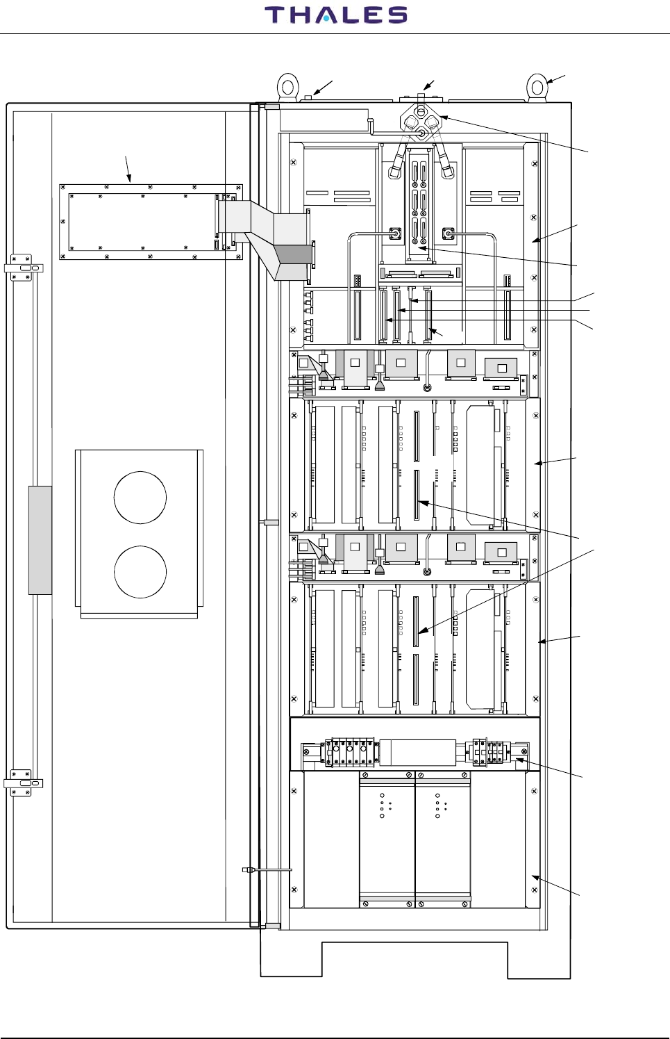
955 900 031C DME 415/435 -Technical Manual
Vol. 1-Section 1-General Information
1-22 THALES Italia S.p.A.- A. S. D. Vers. D, September 2005
DH
B
C
E
J1
F
DH
B
C
E
J1
F
AFI
MDM 1(opzion.)
MDM 2 (opzion.)
TX 1
DMD 1
DPR 1
RX 1
MON 1
PWS 1
DPX 2
DPX 1
TX 2
DMD 2
DPR 2
RX 2
MON 2
PWS 2
AC/DC 1
Module OK
Main s OK
V adj
-TP
+
-
AC/DC 2
Module OK
Mai ns O K
V adj
-TP
+
-
OUT OUT
IN IN
N.U.
N.U.
ANTENNA MONITORS PROBES
CONNECTORS ANTENNA
CONNECTOR
Nr. 4 eyebolts
for to be lifting
COAX
RELAY
50 Ohm
Dummy Load
RF TEST
PATCH PANEL
RF AMPL/DPX
SUBRACK
TRX/MON (1)
SUBRACK
TRX/MON (2)
SUBRACK
Terminal BAR
BCPS Subrack
LCSU unit
Rear view
Documents holder
Figure 1.6. DME 415 – Front view with anterior door opened – Full Dual version
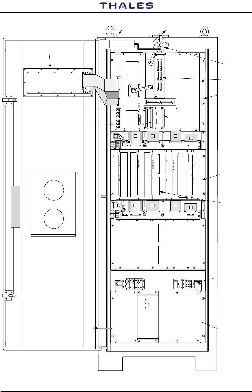
DME 415/435 -Technical Manual
Vol. 1-Section 1-General Information 955 900 031C
Vers. D, September 2005 THALES Italia S.p.A.- A. S. D. 1-23
DH
B
CE
J1
F
AFI
TX
DMD
DPR
RX
MON
PWS
DPX
AC/DC
Mod ule OK
Main s OK
V adj
-TP
+
-
OUT
IN
TKW
N.U.
MAINS48Vdc
IN
54 Vdc OUT
N.U.
MDM 1(option)
MDM 2 (option)
DH
B
CE
J1
F
50 Ohm
Dummy Load
Nr. 4 eyebolts
for to be lifting
COAX
RELAY
RF TEST
PATCH PANEL
RF AMPL/DPX
SUBRACK
TRX/MON (1)
SUBRACK
Terminal BAR
BCPS Subrack
LCSU unit
Rear view
ANTENNA MONITORS PROBES
CONNECTORS
ANTENNA
CONNECTOR
Documents holder
Figure 1.7. DME 435 Single version – Front view with anterior door opened
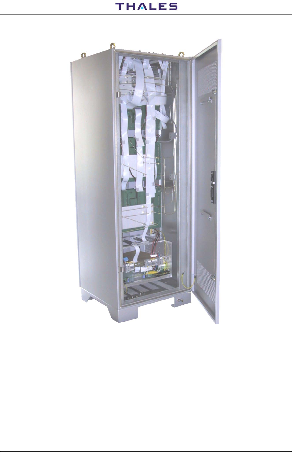
955 900 031C DME 415/435 -Technical Manual
Vol. 1-Section 1-General Information
1-24 THALES Italia S.p.A.- A. S. D. Vers. D, September 2005
Figure 1.8. DME 435 – Rear side view of the cabinet
NOTE: Rear view valid for both cabinets type
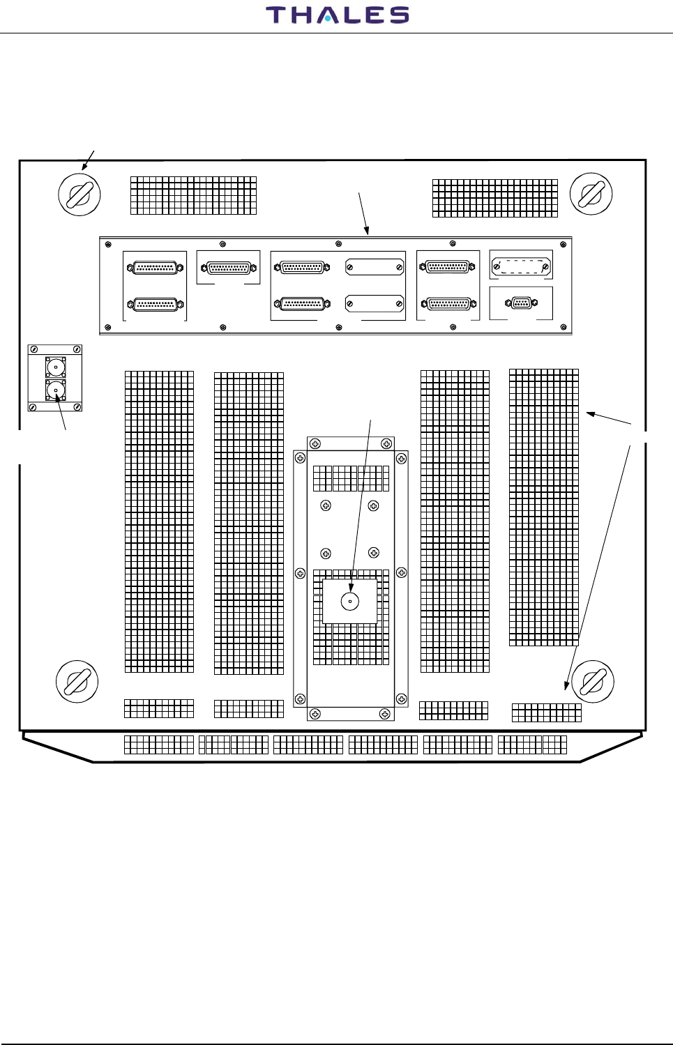
DME 415/435 -Technical Manual
Vol. 1-Section 1-General Information 955 900 031C
Vers. D, September 2005 THALES Italia S.p.A.- A. S. D. 1-25
NOTE: Top end valid for both cabinets type
SK6
TACAN ANTENNA
PL7
TEL. LINES
1-6= LINE 1 3-8=LINE 2
ASSOC. FACILITY
AF1
AF2
SK4
SK5
PARALLEL PORT
IN (16/31)
PL4
SK3
OUT(16/31)
SK2
PL3
IN (0/15)
OUT(0/15)
PC (RS232)
SK1
PORT 1 (DCE)PORT 3 (DCE/DTE)
PL2
PL1
PORT 2 (DTE)
SER IAL POR T (R S232)
M2
M1
ANTENNA CONNECTOR
"N" type Female
N° 4 eyebolts
Front
Rear
AIRING GRID
I/O PANEL
NOT to SCALE
A
NTENNA MONITORS
CONNECTORS
"N" type Female
Figure 1.9. DME 415/435 – Top view

955 900 031C DME 415/435 -Technical Manual
Vol. 1-Section 1-General Information
1-26 THALES Italia S.p.A.- A. S. D. Vers. D, September 2005
1.6 EQUIPMENT FUNCTIONAL DESCRIPTION
1.6.1 General Overview
The DME 415/435 system consists of hardware based on RF and video PBA, and of software that
largely controls the hardware. In order to explain these functions, the description is divided in following
main parts as by composition of the equipment (see also the simplified general block schematic with
the main RF signals on fig 1.10.
The system is subdivided into the following units (dual or single version):
- Transponder (RX, DPR, DMD, TX-100, PWS)
- Transmitter Amplifier 1kWp (TKW) (only for DME 435)
- RF path – Duplexer and Coax. Relay (DPX, KCX, MKCX and TAI dummy)
- Monitor (MON)
- Local I/O (LCSU)
- Associated Facility Interface (AFI)
- AC/DC Power supply (BCPS)
- Antenna
- Modem (optional)
- Remote Control Indication (RCSI/RCSE or MCS)
Transmitter and monitor are controlled by their own individual microprocessors. Both communicate with the
LCSU, controlled by its own microprocessor.
The transponder processor performs the following main tasks:
- General management of the transponder
- Digital and video processing
- Control/adjustment of main delay
- Control/adjustment of modulation for peak power and pulse shape
The monitor processor performs the following main tasks:
- General management of the monitor
- RF signal generation of interrogation pair for executive monitoring
- Evaluation of the transponder reply signals and receiver sensitivity (in Antenna and Dummy load)
- Execution of appropriate actions in case of fault detection (station changeover or shutdown)
- Ensuring of its own performance independent of environmental conditions and component
aging (selfcheck)
The software packages (i.e., transponder SW, monitor SW, LCSU SW, PC WIN Supervisor, WIN ADRACS
or MCS and WIN EQUIPMENT MANAGER) looks after and supports the most important tasks as follows:
- Startup (alignment and calibration of the set up)
- Modulation and transmitter control
- Signal generation
- Monitoring the output signal of the transponder
- Support in system repair and maintenance
- Operation of the system (local/remote)

DME 415/435 -Technical Manual
Vol. 1-Section 1-General Information 955 900 031C
Vers. D, September 2005 THALES Italia S.p.A.- A. S. D. 1-27
The Local I/O (LCSU) processor performs the following main tasks:
- Communication via serial line RS232 with the monitor(s) and via serial line RS485 with transponders
- Beacon-operator interface via Personal Computer
- Basic beacon-operator interface via the Control Panel front door
- Check of the settings of equipment
- Connection to one or more remote control centers through switched or dedicated telephone lines
- Communication via modem with remote monitoring and site control
- History management
The Duplexer and RF path performs the following main tasks:
- Exchanges the RF path of the main transponder and of the stand-by transponder on the antenna and on
the internal dummy load
- Coupling signal for monitoring interrogation
- Coupling signal for Pilot pulse
- Manual RF test with patch panel
1.6.2 DME 415/435 System Functional Description
The beacon comprises the following main parts:
− I/O system (LCSU, RCSI/RCSE or MCS, SI, PC, MDM);
− Transponder (RX, DPR, DMD, TX100, PWS);
− 1kWp Amplifier (TKW only DME435)
− RF path (DPX, Patch-panel);
− Monitoring (MON);
− Interface (AFI) and (TAI dummy);
− AC/DC power supply (BCPS).
− DME Antenna
The beacon can also be configured as single transponder either with one or two monitor(s).
The simplified functional block diagram of the dual configuration is shown in figure 1.10.
The simplified functional block diagram of the main RF signal path is shown in figure 1.11
A coaxial transfer switch (controlled by Monitors) is used to the transponder(s) either with the antenna line
(main transponder) or with the internal dummy load (stand-by transponder) (see figure 1.10).
The antenna probes are used to monitoring the reply RF signals (figures 1.10 and 1.11)
Figures 1.12 and 1.13 are simplified functional block diagrams of the I/O and power supply systems
respectively.
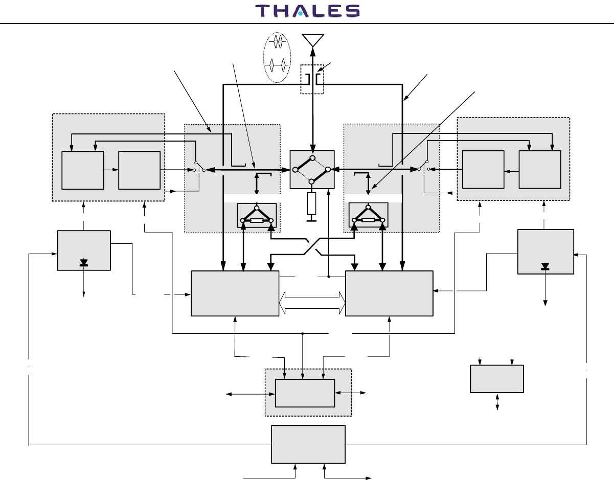
955 900 031C
DME 415/435 -Technical Manual
Vol. 1-Section 1-General Information
Vers. D, September 2005
THALES Italia S.p.A.- A. S. D. 1-28
1-28
Transponder 1 (TRX-1)
PWS-1
status
ch-over
RS 232 RS 232
REMOTE
control unit /PC
Local PC
DPX-1
RX TX
ANTENNA
MONITOR
PROBES
DPX-2
RX
TX
Transponder 2 (TRX-2)
COAX
RELAY
5V, ±15V
5V, ±15V
BCPS
MAINS BATT.
PWS-2
5V, ±15V
MON-1 MON-2
LCSU
Local I/O
RS-485 RS-485
+48
Vdc
+48
Vdc
5V
to LCSU
AFI
to/from
TRX1 TRX2
Assoc. Facility
DC/DC
Power Supply DC/DC
Power Supply
Battery Charger
AC/DC Power Supply
RF Reply pulses
for monitoring
RF Interrogation pulses
for monitoring
RF Interrog./Reply
pair pulses
Monitor Monitor
ADDER/DIVIDER
17dB
coupler
20 dB
coupler
X Mode
Y Mode
Pilot Pulse
RS-485
5V
to LCSU
to Associated
Facility
ADDER/DIVIDER
Figure 1.10. DME 415/435 – Simplified general block diagram
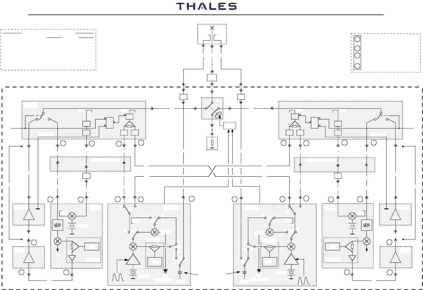
DME 415/435 -Technical Manual
Vol. 1-Section 1-General Information 955 900 031C
Vers. D, September 2005 THALES Italia S.p.A.- A. S. D. 1-29
1-29
63 MHz
DPX- 2
AB
B
A
AB
A
B
S2
A
A
A
B
&&
10
dB
10
dB
dB
dB
dB
dB
dB dB
66
66
dB dB
17
13 13
17
10
dB
10
dB
10
dB
(SEE NOTE) ( SEE NOTE)
112
3
23
4
4
(SEE NOTE)
ANT
10
dB
(SEE NOTE)
"SMA""SMA" "SMA" "SMA" "SMA""SMA"
MONITOR SWITCHES POSITION
SWITCH
Interrog. for CALIB. B X B A X
Interrog. to RX1/2 A A/B B A X
REPLY from TX1/2 B A/B A X X
ANTENNA Monit. PROBE X X X X B
DIAGNOSTIC X X X B A
S1 S2 S3 S4 S5
PLUG-IN Type COAX CONNECTOR
Module REF POSITION
4
3
2
1
1, 2, 3, 4 = DPX
1, 2, 3 = RX, MON
1, 2, = TX
21 dB 21 dB
KCX
50 ohm
Dummy
Load
3232
1
3
2
3
21
RF PATCH PANEL 1
Pilot Pulse
MON I/O
RX IN
63 MHz
17dB
RX 1
TKW1
SYNTH.
VCO
TX 1
IF
59 MHz
VCO
SYNTH.
S2
S1
S3
S5
S4
DET
DET-A
AB
B
A
B
A
AB
B
A
DET-A
DET
59 MHz
VCO
SYNTH.
BA
A
A
A
B
B
B
A
S2
S3
S1
S4
S5
MON 1 MON 2
20 dB 20 dB
BRX 2 TKW2
17dB
VCO
SYNTH.
TX 1
IF
20 dB 17dB
DPX 1
LRXINHD1
LRXINHM1
LRXINHD2
LRXINHM2
MON I/O RX IN
Pilot Pulse
RF PATCH PANEL 2
17dB 20 dB
21
1
12
NOTE: 10 dB Attenuators used when TKW is present
DME 415/435
1
KCXM
Transfer
coax relay
Reply Measur. and
Diagnostic
Purpose
MEASUREM. MEASUREM.
63 MHz 63 MHz
"N" "N" "N"
W1 W2W2
"N" "N" "N"
"TNC"
"TNC"
"TNC"
"TNC"
"N"
"N"
"N"
"N"
W6
"N"
W6
"N"
"SM A "
W8b
W7b
W5b
W5a W7a W8a
W9
W9
W3a
W3b
W3
W4
W9
W9
W10
W10 W8a W7a W5a
W7b
W8b W5b
"SMA"
W3
W3a
W4
W3b
"N"
"N"
"N"
"N"
W1=Antenna (Ext)
W2=Antenna Probes (Ext)
W3=TX to DPX
W3a=TKW to DPX (DME435)
W6=DPX to KCX
W7a=RX test via Patch Panel
W7b=RX test via Patch Panel
ED.: 1 - 1999
BPF
(opt)
W4=RX to TX
W5a=DPX to RX via Patch Panel
W5b=RX to DPX via Patch Panel
INTERCONNECTING COAX CABLES
W8a=MON Interr/Reply via Patch Panel
W8b=MON Interr/Reply via Patch Panel
W9=MON Interr/Reply (Cross interconnecting)
W10=Antenna Probes
W3b=TX to TKW (DME435)
INTERCONNECTING COAX CABLES
Figure 1.11. DME 415/435 – Main RF path signals - General simplified block diagram
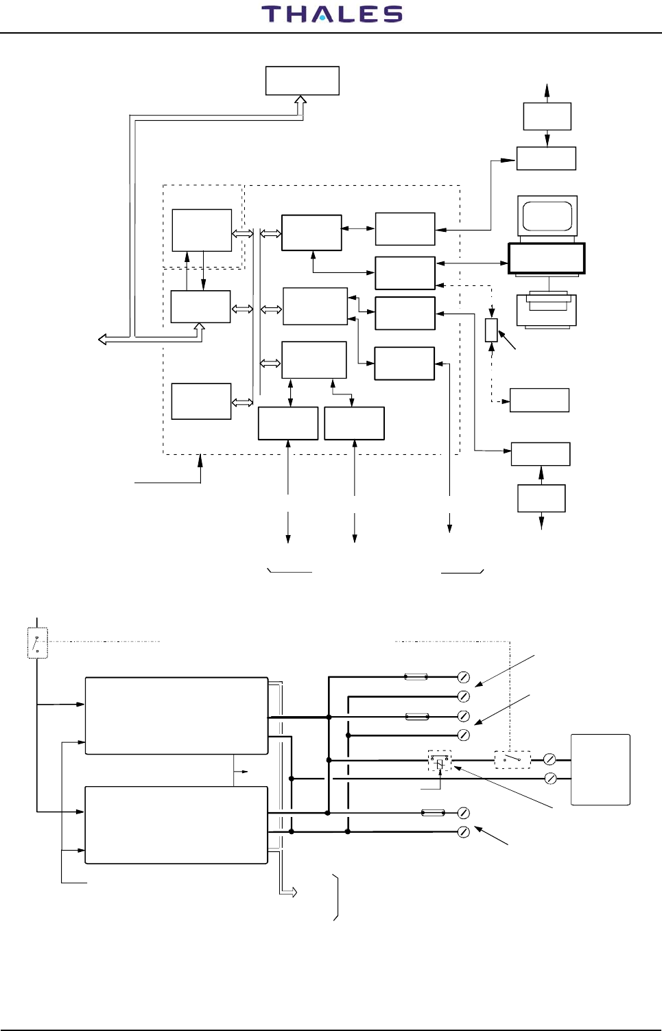
955 900 031C DME 415/435 -Technical Manual
Vol. 1-Section 1-General Information
1-30 THALES Italia S.p.A.- A. S. D. Vers. D, September 2005
PARALLEL
I/O
CPU
MODEM 1
SERIAL
COMMUNICAT.
CONTROLLER
SERIAL
COMMUNICAT.
CONTROLLER
PC
PRINTER
STATUS SITE
INDICATION
TELEPH. LINE
(PC Remote or RCSI)
RS232
DRIVER
RECEIVER
(CSB module)
CONTROL
PANEL &
STA TUS IND.
INC module
AUXILIARY ON/OFF
Controls and Indications
MON1 MON2
+5 V
ESD
protection
(option)
RS232
DRIVER
RECEIVER
RS232
DRIVER
RECEIVER
RS485
DRIVER
RECEIVER
SERIAL
COMMUNICAT.
CONTROLLER
RS232
DRIVER
RECEIVER
TRX1
TRX2
RS232
DRIVER
RECEIVER
MODEM 2
TELEPH. LINE
(PC Remote or RCSI)
ESD
protection
(option)
RS 232
Seial Line RS 232
Seial Line
RS 485
Seial Line
LCSU unit
SI446
RS422
RS232
Asyncro Conv. Interf.
TRANSPONDERS Communication
Figure 1.12. DME 415/435 – Local I/O system general block diagram
AC/DC 1
600 W/10A
BATT.
+
-
+
-
+
-
+
-
AC/DC 2
600 W/10A
+
+
-
-
MAINS
+
-Typical
50A/h-48V
BREAKERS on external Electrical Switchboard (recommended)
External BATT RELAY
SWITCH (Optional)
ACFTY1
ACFTY2
MAINS1
MAINS2
BPDPL
Command ON/OFF (N.U.)
(From LCSU) INDICATIONS
(To LCSU)
Fuse 10A
Fuse 2A
48V to
service purpose
Fuse 10A
*)
*)
48V to
transponder/monitor 2
48V to
transponder/monitor 1
Figure 1.13. DME 415/435 – AC/DC Power Supply system & Battery Charge - Block diagram

DME 415/435 -Technical Manual
Vol. 1-Section 1-General Information 955 900 031C
Vers. D, September 2005 THALES Italia S.p.A.- A. S. D. 1-31
1.6.3 I/O SYSTEM - Functional description
Consist of the Local and Remote Control & Maintenance System.
The I/O system is totally modular; it is able to meet any type of requirement that may arise in an installation.
Main features of the System are:
• Control/monitoring of the equipment by means of a standard Personal Computer, and/or Remote Control
& Status Indicator and/or a Status Indicator of the beacon main indication.
• Control and monitoring of the beacon and its associated equipment (only on customer request), if any
(e.g. VOR/ILS), by using a Personal Computer.
• Possibility to control, monitor and maintain the equipment station by using the public switched network
or dedicated telephone lines
It is composed by the following main parts:
– Local Control & Status Unit "LCSU" housed inside the equipment, consisting of the Control Status
Board module (CSB), the Indication and Control module (INC) and I/O panel
– Remote Control & Status Indicator "RCSI 446, RCSE 443 or MCS" (optional).
– Status Indicator "SI 446" (optional).
– standard Personal Computer IBM compatible (optional).
– Modem (optional).
1.6.3.1 I/O Local site
At the local site, the beacon-operator interface consists of:
− Module INC (LCSU) control and indication front panel;
− Personal Computer (optional), which allows the operator to completely control and monitor the beacon;
− Status Indicator SI446 (optional), which may be installed in the equipment control room or control
tower.
It is handled by the LCSU unit, which also controls the communication with other equipment and/or
device(s), through RS-232C serial interface ports or through modem and telephone lines.
− The I/O Panel (figure 1.14) located on the top end of the cabinet is complete with a set of
interconnection connectors interface the external equipment or devices.
A typical configuration of the local site set-up is shown in figure 1.15.
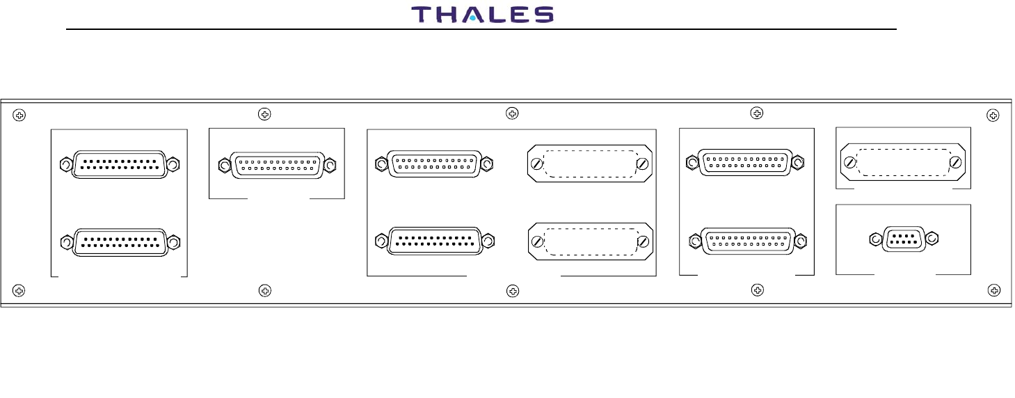
DME 415/435 -Technical Manual
Vol. 1-Section 1-General Information 955 900 031C
Vers. D, September 2005 THALES Italia S.p.A.- A. S. D. 1-32
1-32
SK6
TACAN ANTENNA
PL7
TEL. LINES
1-6= LINE 1 3-8=LINE 2
ASSOC. FACILITY
AF1
AF2
SK4
SK5
PARALLEL PORT
IN (16/31)
PL4
SK3
OUT(16/31)
SK2
PL3
IN (0/15)
OUT(0/15)
PC (RS232)
SK1
PORT 1 (DCE)PORT 3 (DCE/DTE)
PL2
PL1
PORT 2 (DTE)
SERIAL PORT (RS232)
PL1 = UNAVAILABLE if MDM 2 IS USED
PL2 = UNAVAILABLE if MDM 1 IS USED
SK1 = PC connection
UNAVAILABLE if
PC connector on
FRONT PANEL
is USED
SK2 = N° 16 AUXILIARY ON/OFF OUT SIGNALS (standard)
PL3 = N° 16 AUXILIARY ON/OFF IN SIGNALS (standard)
(e.g. possible Site Status Indication)
SK3 = N° 16 AUXILIARY ON/OFF OUT SIGNALS (optional)
PL4 = N° 16 AUXILIARY ON/OFF IN SIGNALS (optional)
SK4 = Associated Facility EQPT 1
SK5 = Associated Facility EQPT 2
SK6 = N.U.
PL7 = N° 2 Telephon Line
Internal MODEM connected
Figure 1.14. I/O Panel
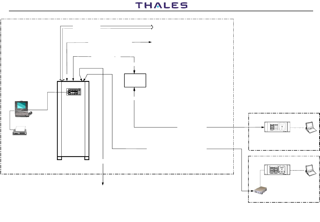
955 900 031C
DME 415/435 -Technical Manual
Vol. 1-Section 1-General Information
Vers. D, September 2005 THALES Italia S.p.A.- A. S. D. 1-33
1-33
RS 232
STATUS INDICATOR
SI 446 - 2/8
WARNING
NORM AL
ALARM
1
ON
SIL
LAMP
TES T
EQUIPMENT STATUS SI
WARNING
NO R M AL
ALARM
2
CONTROL ROOM
RS 232
PC
RS 422
STATUS INDICATOR
SI 446 - 2/8
WARNING
NORM AL
ALARM
1
ON
SIL
LAM P
TEST
EQUIPMENT STATUS SI
WARNING
NORM AL
ALARM
2
RS 232
Modem
PC
RS 232
TELEPHONE LINE CONNECTION WITH A
REMOTE CONTROL MONITORING CENTRE
SERIAL LINE (B) (RS-232) OTHER EQUIPMENT (I. E.,
VOR, EXTERNAL MODEM, ETC.)
Asyncronous
Converter
Interface
CONTROL TOWER
OPTION 1
OPTION 2
(P C OPTION)
PARALLEL LINE ON/OFF DATA
(OTHER EQUIPMENT or DEVICE e.g SITE STATUS )
EQUIPMENT ROOM
PL7
PL2
PL3
SK2
NOTE 1: C&D line UNAVAILABLE if
A&B line ARE USED and viceversa
NOTE 2: On OPTION 1&2
possible use of
RCSI 446-2/8 Remote Control
PL1
DME
415 / 435
Switched or dedicated teleph. LINE ( C)
RS 422
SERIAL LINE (A)
RS 232
LINE (D)
SERIAL LINE (max. 1km)
(or dedicated line)
Figure 1.15. Local site set up – Typical configuration
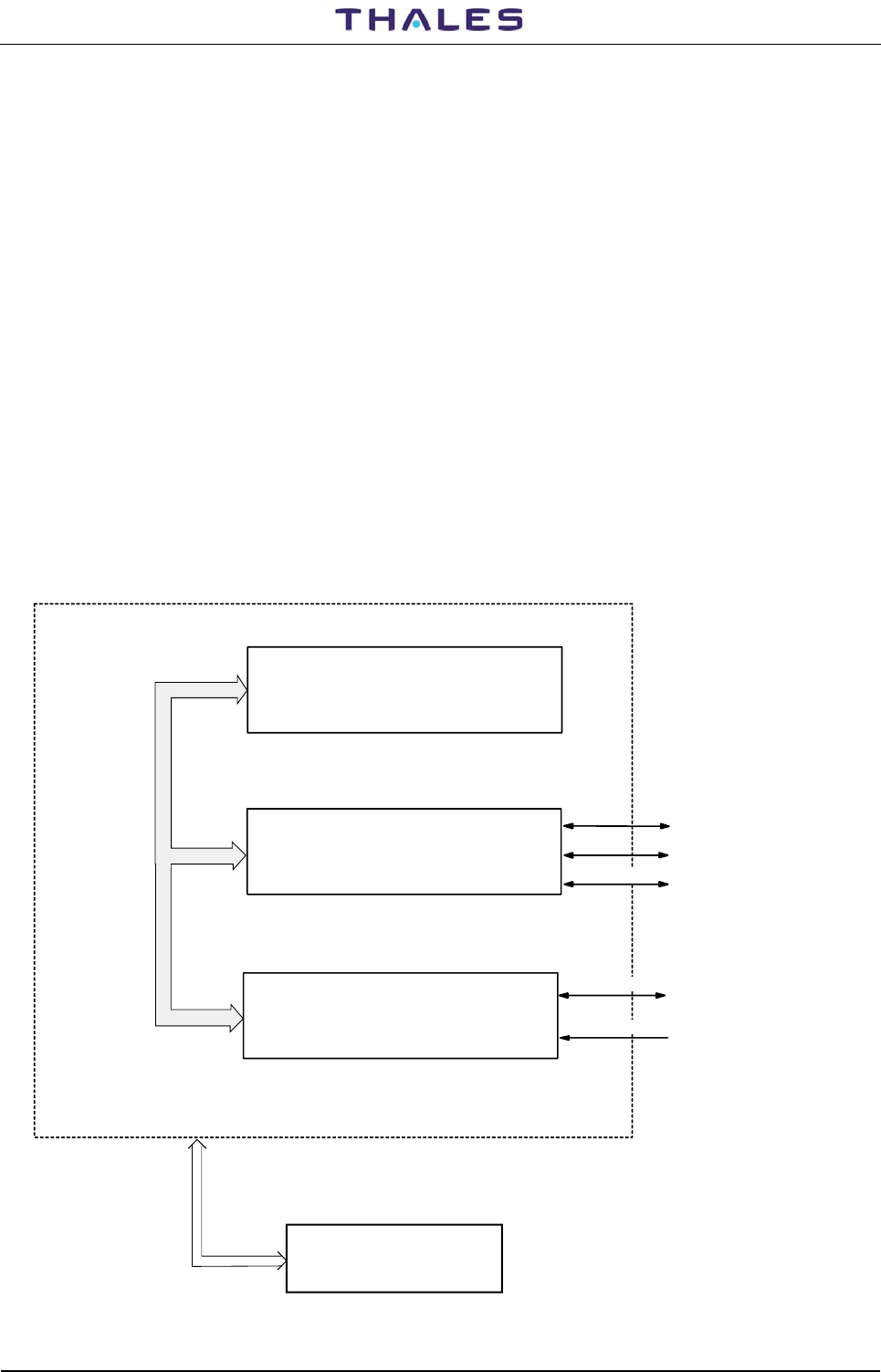
955 900 031C DME 415/435 -Technical Manual
Vol. 1-Section 1-General Information
1-34 THALES Italia S.p.A.- A. S. D. Vers. D, September 2005
1.6.3.2 LOCAL CONTROL & STATUS UNIT (LCSU)
The LCSU unit is the local main unit connecting the equipment to the remote control system. It also handles
the communication with remote monitoring and control sites, which takes place also through modem and
telephone line(s). It is mounted into the equipment cabinet but it is a functionally separate block. The LCSU
is powered by the service voltages of the DME equipment.
Its main functions:
• sends basic controls to the equipment;
• displays the status of the equipment ;
• interfaces modem(s) connecting the equipment with remote units or PCs;
• interfaces the local PC to control-monitor the equipment and to perform maintenance operations at
the site;
• interfaces the co-located equipment (only on customer request).
• manages the two modems (optional, placed inside the equipment) that operate with dedicated or
switched lines up to 28.800 bps.
LCSU consists of the following parts (figure 1.16):
• the Control & Status Board (CSB 186 module) that carries the unit management software.
• the control panel and the status indicator (INC module) used to forward the basic controls and to display
the equipment operating status.
INC
INDICATION &
FRONT PANEL
CSB
CONTROL & STATUS BOARD
CPU & MEMORIES
I/O PARALLEL LINES
SERIAL LINES COMMUNICATION
To I/O PANEL -IN&OUT
To PC
To Equipment
Port 1
Port 2,3
AUX ON/OFF
CONTROLS
Port 4,5,6
To I/O PANEL
AUX ON/OFF n° 12 IN from Equipment
Figure 1.16. LCSU - Simplified Block Diagram
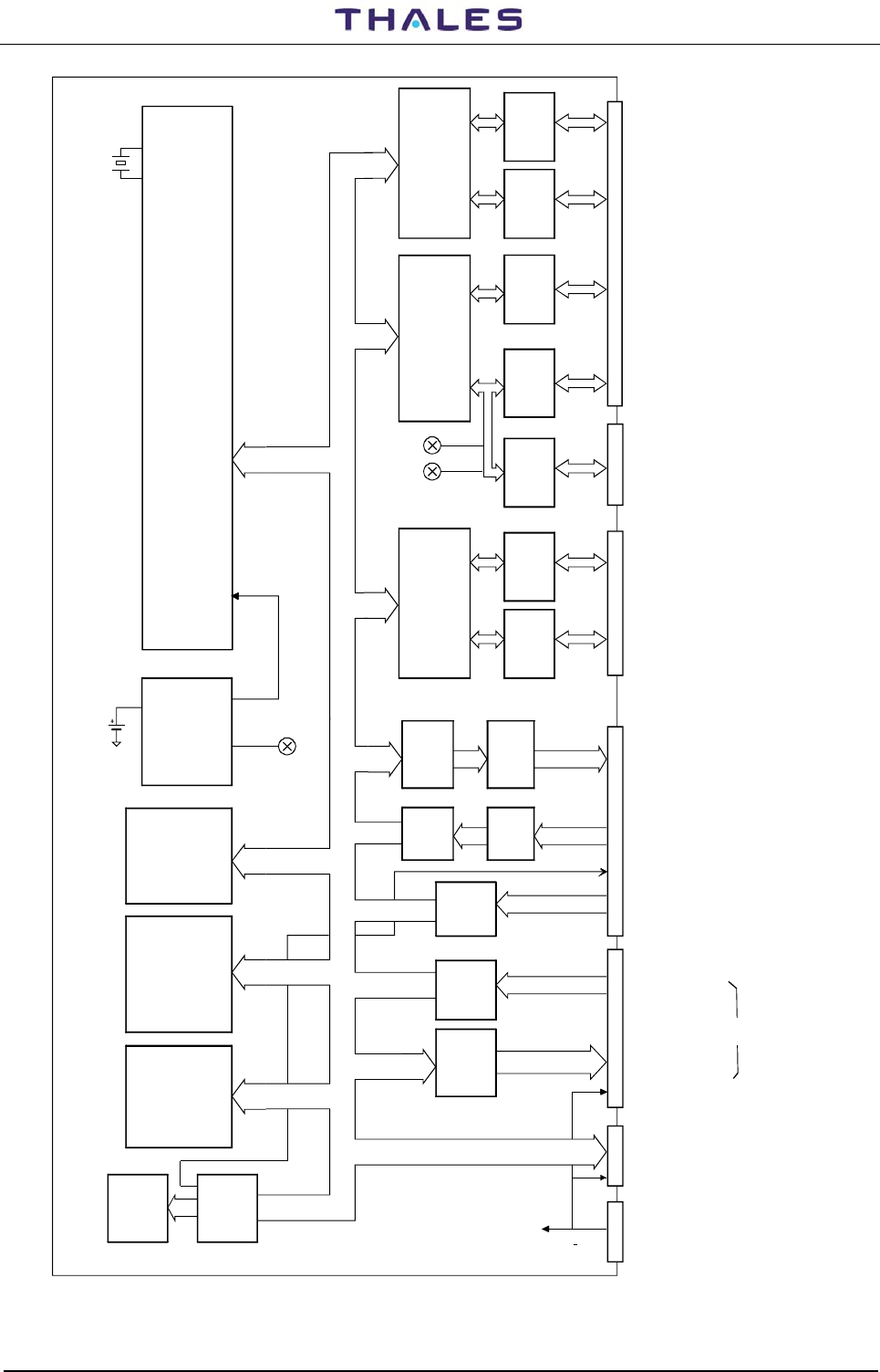
DME 415/435 -Technical Manual
Vol. 1-Section 1-General Information 955 900 031C
Vers. D, September 2005 THALES Italia S.p.A.- A. S. D. 1-35
CHANNEL 2
RS232
DTE
CHANNEL 3
RS232
DTE/DCE
CHANNEL 4
RS232
DCE
CHANNEL 4
RS485/422
CHANNEL 5
RS232
DTE
CHANNEL 6
RS232
DTE
PARALLEL
INPUT/OUTPUT
CONTROLS
from KEYBOARD
INDICATION to
FRONT PANEL
BUS for
EXPANSION
CSX module (option)
POWER
SUPPLY
M21
M18
M17
M32
M53
M30
M22
CHANNEL 1
RS232
DCE
DRIVER
RECEIVER
RS232C
DRIVER
RECEIVER
RS232C
DRIVER
RECEIVER
RS232C
DRIVER
RECEIVER
RS232C
DRIVER
RECEIVER
RS485
DRIVER
RECEIVER
RS232C
DRIVER
RECEIVER
RS232C
SOLID
STATE
RELAYS
OUTPUT
REGISTER
INPUT
REGISTER
OPTO
COUPLER
INPUT
REGISTER
INPUT
REGISTER
OUTPUT
REGISTER
OUTPUT
REGISTER
SERIAL
EEPROM
2k x 8
EPROM
1 Mbit
RAM - 1Mbit
Battery
NI-CD
3,6V Reset
Watch-Dog
and Battery
BackUp
Circuit
Watch Dog
Indication
RESET
CPU
SERIAL
COMMUNIC.
CONTROLLER
SERIAL
COMMUNIC.
CONTROLLER
SERIAL
COMMUNIC.
CONTROLLER
+5V,+15V
16
16
4
8
RXD
TXD
OU 0...4
Indication
To SK1 PC
I/O Panel
To PL2 MDM1
I/O Panel
To PL2 MDM2
I/O Panel
To Transponders (1&2)
(DMD modules)
N.U.
To MON 1
module
To MON 2
module
To SK2
and PL3
I/O Panel
and BCPS
To INC
module
Socket N.U.
Figure 1.17. CSB module – Simplified Block Diagram

955 900 031C DME 415/435 -Technical Manual
Vol. 1-Section 1-General Information
1-36 THALES Italia S.p.A.- A. S. D. Vers. D, September 2005
1.6.3.2.1 CONTROL AND STATUS BOARD - CSB module – Functional description
The main functions of the CSB module (see figures 1.18 block diagram) are as follows:
− management of interfacing between the equipment and remote system;
− up-dating of the remote site unit;
− communication with the monitors on the RS-232C serial links;
− communication with the transponder equipment on the RS-485 serial link;
− driving of the indications and acquisition of the commands of the INC module
− management of the RS-232C serial communication line with the PC terminal;
− management of the RS-232C serial communication line towards the MODEM and towards an
optional external MODEM for connection to specific remote controls on a telephone line;
− management of the ON/OFF type input and output auxiliary signal using the parallel ports;
− storage of the system configuration in a non-volatile memory (EEPROM);
− management of the calendar for the entire system;
− management of the RS-232C and/or RS-485 serial communication lines that can be used for any
associated equipment connected on a serial link.
− History management
− Management of control function line: Beacon Restart, Automatic Routine check, Warning detection,
Alignment of the Parameter of the intelligent units (Monitors, DMD modules), Searching and Building
of the Data requested by the Remote/Local site through PC
Through the CPU and program memories, the CSB module manages:
− INC Module (Indications and Controls);
− local operator interface through PC;
− interface with remote operator via modem to RCSI/RCSE (Remote Control and Status Unit) or MCS by
means of dedicated or switched telephone line;
− SI 446 (Status Indicator) auxiliary indicator via the parallel ports;
− association between auxiliary ON/OFF input and output lines (parallel ports);
− serial channel operation;
− an RTC (Real Time Clock) calendar with rechargeable buffer battery;
− I/O configuration non-volatile memories.
The composition of the CSB module, shown in figure 1.18, consists in the following function blocks:
− CPU and memories;
− 6-channel serial lines;
− Parallel ports with 16 input and 16 output lines.
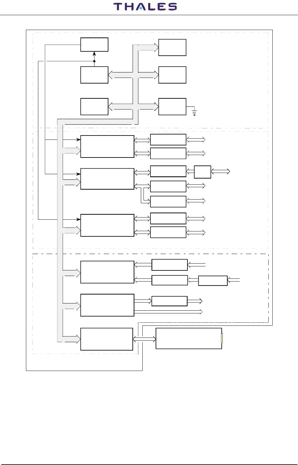
DME 415/435 -Technical Manual
Vol. 1-Section 1-General Information 955 900 031C
Vers. D, September 2005 THALES Italia S.p.A.- A. S. D. 1-37
OPTO
ISOLATOR
OPTO
ISOLATOR
CPU
uP 80C188
BAUD RATE
GENERATOR
MEM
SRAM - EPROM
MEM
PARALLEL
EEPROM
MEM
SERIAL
EEPROM
CONFIGURATION
MEMORY
RTC
REAL TIME
CLOCK
SCC
SERIAL COMMUNICATION
CONTROLLER
DRIVER RECEIVER
DRIVER RECEIVER
SCC
SERIAL COMMUNICATION
CONTROLLER
DRIVER RECEIVER
DRIVER RECEIVER
LINK
JUMPER
DTE/DCE
RS232
RS232
RS232
RS232
DRIVER RECEIVER
RS485
SCC
SERIAL COMMUNICATION
CONTROLLER
DRIVER RECEIVER
DRIVER RECEIVER
RS232
RS232
INPUT
REGISTERS
OUTPUT
REGISTERS
INPUT/OUTPUT
REGISTERS
OPTO SOLID
STATE RELAYS
LINK JUMPER
SELECTOR
INC
INDICATION &
CONTROLS PANEL
BACK UP
BATTERY
RS232 DCE
CHANNEL 1
RS232 DTE
CHANNE L 2
RS232 DTE/DCE
CHANNE L 3
RS232 DCE
CHANNE L 4
RS485
CHANNE L 4
RS232 DCE
CHANNE L 5
RS232 DTE
CHANNE L 6
PARALLEL LINE
N° 8 INPUT GND LEVEL
PARALLEL LINE
N° 8 INPUT
PARALLEL
N° 16 OUTPUTS
CPU & MEMORIES
SERIAL LINES COMMUNICATION
I/O PARALLEL LINES
CSB CONTROL & STATUS BOARD
PC
RS232
BUS
LEVEL & POLARITY PRESETTING
N° 5 OUTPUTS TTL
N.U.
Figure 1.18. CSB module – General Block Diagram
1.6.3.2.1.1 CPU and Memories
The 80C188 type microprocessor works internally with a frequency of 7.3728 MHz by means of a double
frequency quartz (it is divided internally by the CPU) and it uses integrated circuits UL6,7,8 to manage the
data bus and address buses (see figure 1.19 ). The 14.7456 MHz quartz frequency is used by the baud rate
generator of the SCC (Serial Communication Controller) and passes without alteration from FW2 (in cases
of quartz frequency change, the clock can be divided) to provide the BRGSCC signal.

955 900 031C DME 415/435 -Technical Manual
Vol. 1-Section 1-General Information
1-38 THALES Italia S.p.A.- A. S. D. Vers. D, September 2005
The multiplexed portion of the address bus is stored in two latches (UL6 and UL7) in order to have stable
signals during the various CPU cycles.
The data bus is connected to the peripherals and the memories by a bi-directional buffer (UL8). This
solution has been used, to overcome not bus electric drive problems, but peripheral problems (such as the
RTC that does not release the bus before the CPU starts the next cycle).
A perpetual real time calendar (RTC - Real Time Clock) useful to date the events stored in the “history” is
installed to ensure the data concerning events that have taken place in the history of the TACAN equipment
is picked up. The manual updating of the date is managed by the “Supervisor” program.
The function is provided by the low consumption integrated circuit (4 μA at 2.2 V) UL5 (RTC) that operates
with a 38.768 kHz ceramic quartz.
This updates and supplies the complete actual date to the μP. The RTC memory is not lost when there is no
direct voltage since the BT1 buffer battery is switched onto UL5 from IC UL4 that constantly compares the
+5 Vdc. If this is missing, a switching electronic device enables the BT1 battery.
Under these conditions, the typical life of the rechargeable NiCd battery (3.6 V and 60 mA/h) is approx. six
months.
Through the FW1 circuit (Firmware EPLD - Electrical Programmable Logic Device), the IC UL4
(Supervisory) indicates that the program running will retrigger the timer correctly and consequently LED
“WD” (Watch Dog) RD4 will remain alight, indicating that the program running is correctly active.
In the case of a hardware fault or software failure, LEDs RD4 and OPERATION (of the INC) will not light up,
indicating that the CSB module is not operating correctly.
Integrated circuit IC UL4, besides monitoring the CPU activity, also checks the level of the +5 Vdc; if this
degrades to values below ≤ 4.65 V a “Warning” signal is generated. Integrated circuit IC UL4 also checks
the state of the buffer battery, and through the BATF signal indicates the Warning State.
IC UL16 (serial EEPROM) stores the I/O system configuration data, that does not usually vary a lot; it can
hold data for about 100 years, and this is the reason why another type of less secure memory (RAM) is not
used with a buffer battery.
RESET push-button I1 is used to restore and reinitialize the CPU program.
Integrated circuits FW1 and FW2 are specifically programmed to decode the selection of memories and I/O
peripherals, and to generate a clock for the serial port controllers.
The EPROM memories for the program (M7) and SRAM (UL9) have memories a capacity of 1 Mbit (128k x
8), but other sizes can be installed, up to the maximum μP addressing capacity (8 Mbit).
There is another socket on the printed circuit (not usually used) where an SRAM/EEPROM with capacity up
to 8 Mbit can be installed.
The UL9 SRAM memory where the events (history) data are loaded is always powered. When there is no +5
Vdc supply, this is substituted by the rechargeable buffer battery. By correctly setting the jumpers on the
CSB board, the other optional memories can also be supplied by the buffer battery. In this case, the battery
life will be reduced to 2 months.
For the memory rate, with a 10 MHz clock and a 16 MHz CPU, memories with an access time of 100 ns are
sufficient.
UL2 is an analog switch that electrically isolates the SRAM when operating by battery.
When the LOW LINE signal is present, activated each time the VDC drops below 4.65 V, the RTC circuit is
electrically isolated from UL2 to prevent undesired access and reduce consumption to a minimum in stand-
by conditions (battery powering).
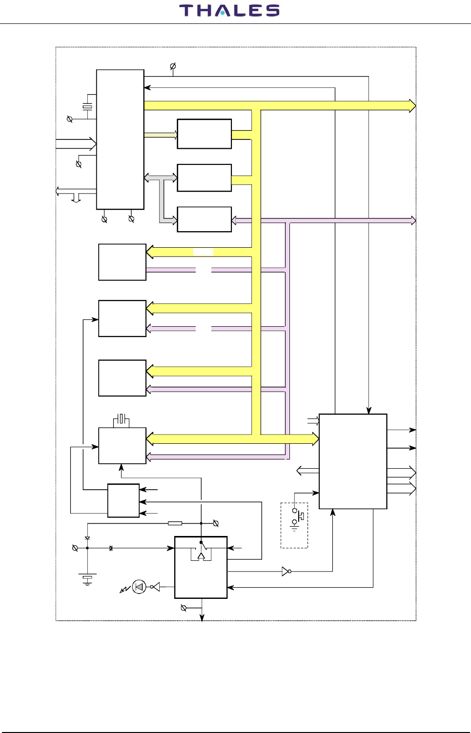
DME 415/435 -Technical Manual
Vol. 1-Section 1-General Information 955 900 031C
Vers. D, September 2005 THALES Italia S.p.A.- A. S. D. 1-39
CPU
UL3
14.7456
MHz
Q1
UL6
LATCH
UL7
LATCH
UL8
TRANSCEIVER
FW1- FW2
CLOCK
BAUD RATE
GENERATOR
& DELAYER
M7
EPROM
UL9
SRAM
M8
PARALLEL
EEPROM
UL5
RTC
UL4
mPSUPERVISORY
MEM DECODER
I/O DECODER
BATT & 5VCC
CONTROL
REAL TIME
CLOCK
UL2
ANALOG
SWITCH
Q2
32K x 8
128K x 8
128K x 8
32,768 KHz
+
BT1
GREEN
RD4
WD
UL1d
UL1c AUTORESET
ENABLE
CPU
RESET
I1
BRG
CK
BRGSCC
DEL_WR
WRCS
RDCS
MCS3
PCS
INTSCC
RES
PCS
A BUS
A BUS
A BUS
D BUS
D BUS
D BUS
AS BUS
AD BUS
CSB CPU & MEMORIES
D BUS
A BUS
PROGRAM. FIRMWARE
AN5
AN6
WR
AN7
RD
AN1
INSCC0
MCS
AN3
AN8 BATF
AN2
VBATT
AN4
VBAC
LOWLINE
Vcc
VBAC
WR
WR
Power
Down
+-
WDI
CS9
P 80C188
µ
Figure 1.19. CSB module – CPU and Memories: Block Diagram

955 900 031C DME 415/435 -Technical Manual
Vol. 1-Section 1-General Information
1-40 THALES Italia S.p.A.- A. S. D. Vers. D, September 2005
1.6.3.2.1.2 Serial Lines
There are six serial communication channels in the RS-232C configuration (figure 1.20 block diagram), or
five in the RS-232C configuration and 1 in the RS-485 configuration which can be selected by suitable
jumpers.
The transmission rate is selected during the configuration stage.
Channel 1, 2, 3 and 4 outputs transit on the 64-pin M22 speedy connector that can be used on the I/O panel
connectors SK1, PL1, SK2 for channels 1, 2 and 4 respectively whereas channel 3 is used for
communication with the equipment (of SK2-IRS module). Channel 4 on SK2 is preset in RS-232C
configuration, whereas selecting the M24 connector jumpers it transits on connector M30 (10-pin speedy)
that can be preset in RS-485 configuration. Channel 5 and 6 outputs through connector M53 (34-pin
speedy) are brought onto PL4 and PL2 of the I/O panel.
Serial channel 1
Channel 1, managed by UL21 SCC (Serial Communication Control) and driven by IC “UL22” (RS-232 Driver
Receiver) is in the DCE standard (Data Communication Equipment) RS-232C configuration and is
connected to the PC through connector SK1 on the I/O panel. The PC can be connected to the INC module
SK6 (PC RS232) connector as this is in parallel directly to the I/O panel connector SK1.
Serial channel 2
Channel 2, managed by UL 21 SCC (Serial Communication Control) and driven by IC “UL23” (RS-232
Driver Receiver) is in the DTE standard (Data Terminal Equipment) RS-232C configuration and can be
connected to the possible external modem via PL1 on the I/O panel. Signals synchronizing the receiving
and transmission clocks (RXCK and TXCK) are to be used for modem.
Serial channel 3
Channel 3, managed by UL26 SCC (Serial Communication Control) and driven by IC “UL30” (RS-232 Driver
Receiver) can be either RS-232C DCE or DTE configuration according to the arrangement of the M31
connector jumpers.
It communicates with the beacon through the IRS interface in DCE configuration.
Serial Channel 4
Channel 4, managed by UL26 SCC (Serial Communication Control) and driven by IC “UL29” (RS 232 Driver
Receiver) is in the DCE standard RS-232C configuration, when connected to M22; it is in the RS-422/485
configuration driven by Drivers/Receivers UL24, UL28, UL25, UL31 if connected to M30.
The transformation from the RS-232C configuration to RS-422/485 configuration is preset through the
jumpers of connector M24 that switch the RXD signals either on IC UL29 (RS-232C) or on UL24 (RS-
422/485).
RS-422/485 can be used with 4 or 2 wires by suitably setting the jumpers of connector M25.
RD8 and RD9 LEDs driven by UL1f and UL27b, when flashing, indicate respectively the RXD and TXD data
transit and indicate that channel 4 is working efficiently.
Serial channels 5 and 6
Channels 5 and 6, managed by UL32 SCC (Serial Communication Control) and driven by IC “UL33 and
UL34” (RS-232 Driver Receiver) are in the RS-232C DTE configuration, the use of which is conventionally
defined as connection on PL4 and PL2 of the I/O panel for modem.
NOTE
Generally, the DTE configuration can be directly connected to the
modem and the DCE to the PC. To connect a DCE channel to
another DCE channel or another DTE, a “null modem” adapter is
necessary.
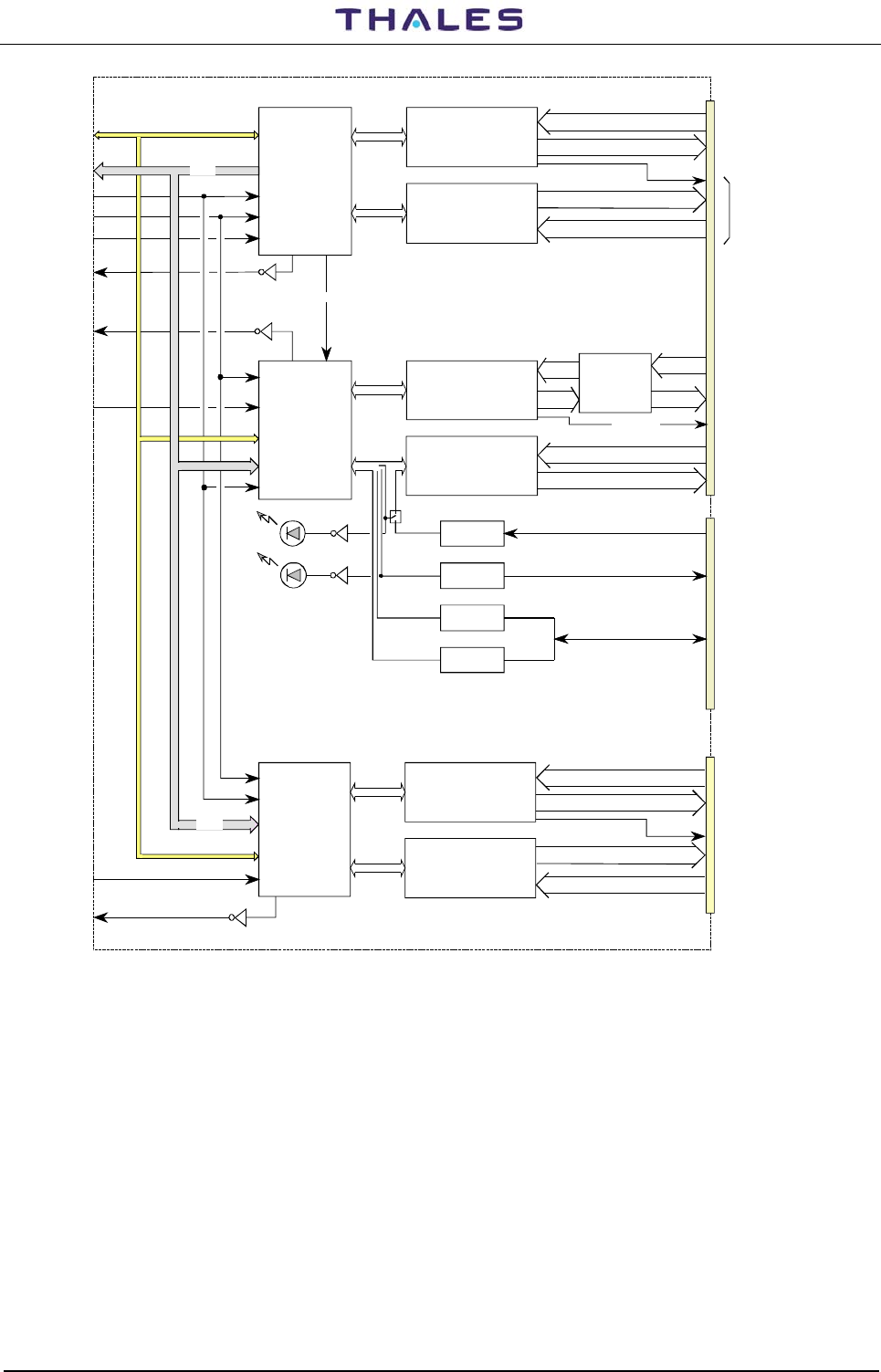
DME 415/435 -Technical Manual
Vol. 1-Section 1-General Information 955 900 031C
Vers. D, September 2005 THALES Italia S.p.A.- A. S. D. 1-41
SCC
SERIAL
COMMUNICATION
CONTROL
DRIVER/RECEIVER
UL21
UL23
DRIVER/RECEIVER
UL22
M22
M30
TXD - RTS - DTR
RXD - CTS - DCD
TXD - RTS - DTR
RXD - CTS - DCD
TXD - RTS - DTR
TXCK
RXD - CTS - DCD -
RXCK
DTE
DTE/DCE
DCE
CH3
CH2
CH1
CH4
To SK
1
PC
MODEM
DTE
DTE
CH5
CH6
SCC
SERIAL
COMMUNICATION
CONTROL
DRIVER/RECEIVER
UL26
UL30
DRIVER/RECEIVER
UL29
N. 6 SWITCH
SELECTOR
DTE/DCE
M31
RXD
TXD
TXCK
RXCK
RECEIVER
DRIVER
DRIVER
RECEIVER
UL24
UL28
UL25
UL31
RS232
RS232
RS232
RS232
RS485 RX
RS485 TX
RS485 CK
CH4
RS485
RS232
DCE
SCC
SERIAL
COMMUNICATION
CONTROL
DRIVER/RECEIVER
UL32
UL33
DRIVER/RECEIVER
UL34
RS232
RS232
GREEN
RD8 UL1f
GREEN
RD9 UL27b
M53
UL1a
UL27a
UL27d
A BUS
D BUS
DEL_WR
BRGSCC
PCS
PCS
PCS
INT
SCC
INT
SCC
INT
SCC
A BUS
1EI
TXD - RTS - DTR
RXD - CTS - DCD
TXD - RTS - DTR
TXCK
RXD - CTS - DCD -
RXCK
M24
RXCK-TXCK
D BUS
Figure 1.20. CSB module – Serial lines: Block Diagram
1.6.3.2.1.3 Parallel ports
The parallel ports are divided into (see figure 1.21):
− Input ports:
8+8 optoisolated lines (galvanic isolation) for the user’s specific applications such as: maximum or
minimum temperature level alarms, presence of smoke, anti-vandal alarms, obstacle lights operation
check etc.;
4 TTL level lines used by the beacon;
6 bits to interface INC panel commands;
16 optional lines on CSX expansion board upon specific request from the user.
− Output ports:

955 900 031C DME 415/435 -Technical Manual
Vol. 1-Section 1-General Information
1-42 THALES Italia S.p.A.- A. S. D. Vers. D, September 2005
16 optoisolated solid state relay lines, that can be used (by the user) as indication signals
5 TTL level lines;
16 bits to interface the INC Module indications;
16 optional lines on the CSX expansion board upon user’s request.
− Input lines. The lines transit from connector M32 to connector PL3 on the I/O panel and are divided as
follows:
8 lines (IAUX 0...7) in two groups of four lines, which have one common for each group.
Each line, by means of its optoisolator, drives two 4-bit input registers (UL19a and UL19b), one for each
group.
The electrical characteristics of the control levels must include a contact to ground, and a typical current
value of 3mA, maximum 30 mA (max. 500 mAp @ 100 μs).
8 lines (IAUX 8...15) made up of two groups of four lines, with one common for each group.
Each line, through its optoisolator, drives two 4-bit input registers (UL20a and UL20b), one for each
group.
The electrical characteristics of the control levels may include a contact to ground or a positive level,
according to the arrangement of the line through the jumpers of connectors M49, M50, M51 and M52
(two lines each) and a typical current of 3 mA, maximum 30 mAp (max. 500 mAp @ 100 μs).
NOTE
Lines IAUX10 to IAUX15 are used internally by the
equipment and therefore are not available for the user.
4 lines (IN 0...3), TTL level, to determine the primary power supply functioning of the BCPS unit.
Each line drives an 8-bit input register (UL14 e).
On I/O panel connector SK4, lines IN0 and IN1, parallel to those on I/O panel connector PL3, are
available through connector M30.
The six bits (CPI1, 2,3) coming from the encoder of the INC module controls, drive the 4-bit input
registers UL13a and UL13b.
− Output lines. The lines transit from connector M32 to I/O panel connector SK4. They are divided as
follows:
16 lines (OAUX 0...15) in four groups of four lines, with one common for each group.
The lines are driven by two output registers (UL17 and UL18) where each register controls 8 outputs.
Each line controls an electronic optorelay that has the following output features:
− Max. applied voltage: 350 Vp;
− Max. current: 100 mAp (100 mA @ ± 7 V load);
− Closing resistance: 50 Ω
− Leakage current at 300 V: 40 μA;
5 TTL lines are also available, three on connector SK4 and two on I/O panel connector PL3.
They are driven by the 8-bit output register UL12 that exchanges the data of the EEPROM serial memory
UL16 via UL15a and the “Serial Clock” and “Serial Data” signals.
Through the 8-bit output registers UL10 and UL11, the 16 bits of the CPD and CPA buses drive the
sequence of indications on the INC Module.
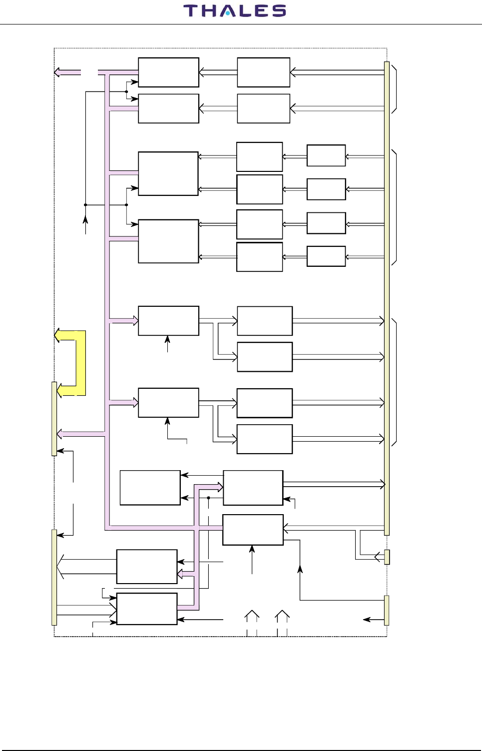
DME 415/435 -Technical Manual
Vol. 1-Section 1-General Information 955 900 031C
Vers. D, September 2005 THALES Italia S.p.A.- A. S. D. 1-43
4BIT INPUT
REGISTER
UL19a
OPTO
INSULATORS
OP9b-OP10a,b-OP11a
IAUX 0..3
JUMPERS
SWITCH
M49
8 BIT OUTPUT
REGISTERS
UL10-UL11
4 BIT INPUT
REGISTER
UL13a,b
8 BIT INPUT
REGISTER
UL14
M21
M17
4BIT INPUT
REGISTER
UL19b
OPTO
INSULATORS
OP11b-OP12a,b-OP9a
IAUX 4..7
4BIT INPUT
REGISTER
UL20a
OPTO
INSULATORS
OP21a,b
IAUX 8.9
JUMPERS
SWITCH
M50
OPTO
INSULATORS
OP22a,b
IAUX 10.11
JUMPERS
SWITCH
M51
4BIT INPUT
REGISTER
UL20b
OPTO
INSULATORS
OP23a,b
IAUX 12,13
JUMPERS
SWITCH
M52
OPTO
INSULATORS
OP24a,b
IAUX 14.15
8BIT OUTPUT
REGISTER
UL17
OPTO RELAIS
OP1-OP2-OP3-OP4
OAUX 0..3
OPTO RELAIS
OP5-OP6-OP7-OP8
OAUX 4..7
8BIT OUTPUT
REGISTER
UL18
OPTO RELAIS
OP13-OP14-OP15-OP16
OAUX 8..11
OPTO RELAIS
OP17-OP18-OP19-OP20
OAUX 12..15
D BUS
CPI 1,2,3
CPD;CPD Bus
M32
+5VCC
±15V
RDCS
D BUS
D BUS
A BUS
PF 1/2
IN 0..3
N° 8 INPUT
N° 8 INPUT
POLARITY & LEVEL
PRESETTING
N° 16 OUTPUTS
To
INC
To
CSX
8 BIT OUTPUT
REGISTERS
UL12
SERIAL
EEPROM
UL16
2kx8
OUT 0..4 N°5 TTL OUTPUT
SCL
RDCS
WRCS
RDCS
WRCS
WRCS
RDCS
WRCS
WRCS
M18
+5VCC
±15V
M30
SDA
BATF
IN 0..3
SDA
N° 4 TTL INPUT
BCPS 1,2,3,4
Figure 1.21. CSB module – I/O Parallel Ports: Block Diagram

955 900 031C DME 415/435 -Technical Manual
Vol. 1-Section 1-General Information
1-44 THALES Italia S.p.A.- A. S. D. Vers. D, September 2005
1.6.3.2.2 LOCAL FRONT CONTROL PANEL
The front panel of LCSU (part of the INC module) is shown in figure 1.22.
It is divided in the following parts:
one dedicated to the unit itself, and one dedicated to the equipment.
1) The part dedicated to the LCSU status contains:
− OPERATION connected directly to the "watch dog signal" of the CPU 186,
− WARNING not used and always off,
− DATA COM not used and always off,
− buzzer (S1),
− button SIL to silence the buzzer and the
− LAMP TEST button;
2) The part dedicated to the equipment comprises the following sections:
beacon MAIN STATUS indications: this section includes the four alphanumerical devices for beacon
site code, the ALARM, WARNING, NORMAL and DATA COM general status indications.
3) DETAILED STATUS indications; these indications are requested by the operator by pressing the
SELECT button, the triangular sign indicates enabling of the following detailed indications:
- ALARM, STBYALRM, FAULTY and BYPASSED are monitor indications:
MON 1/2 alarm, MON 1/2 stand by alarm, MON 1/2 faulty, MON 1/2 bypass
- ON, WARNING, FAULTY and ON ANT are transponder indications:
TX 1/2 on, TX 1/2 warning, TX 1/2 faulty, TX 1/2 on ant.
a) For each MONITOR indication(Mon1 & Mon2):
− ALARM - Means the monitor see an alarm on the transponder on antenna
− STBYALRM - Means the monitor see an alarm on the transponder on dummy load
− FAULTY - Means the monitor found itself wrong
− BYPASSED - Means the monitor is bypassed because the beacon is in Maintenance Mode
b) For each TRANSPONDER indication (TRX1 & TRX2):
− ON - Means the transponder is ON (radiating if it is on antenna)
− WARNING - Means the transponder found a warning condition (e.g. different command by
monitors)
− FAULTY - Means the transponder is faulty
− ON ANT - Means the transponder is on antenna
4. Station control (CONTROL STATION):
− Indication of control enabled by a remote control (ENGAGED),
− Indication of local control enabled (ENABLED).
− Priority activation/de-activation button in local control (REQUEST RELEASE).
− Indication of mains failure (MAINS OFF).
− Indication of optional site alarms (ENV ALARM).
− Indication of optional antenna alarm (ANT FTY) – Not used on the DME
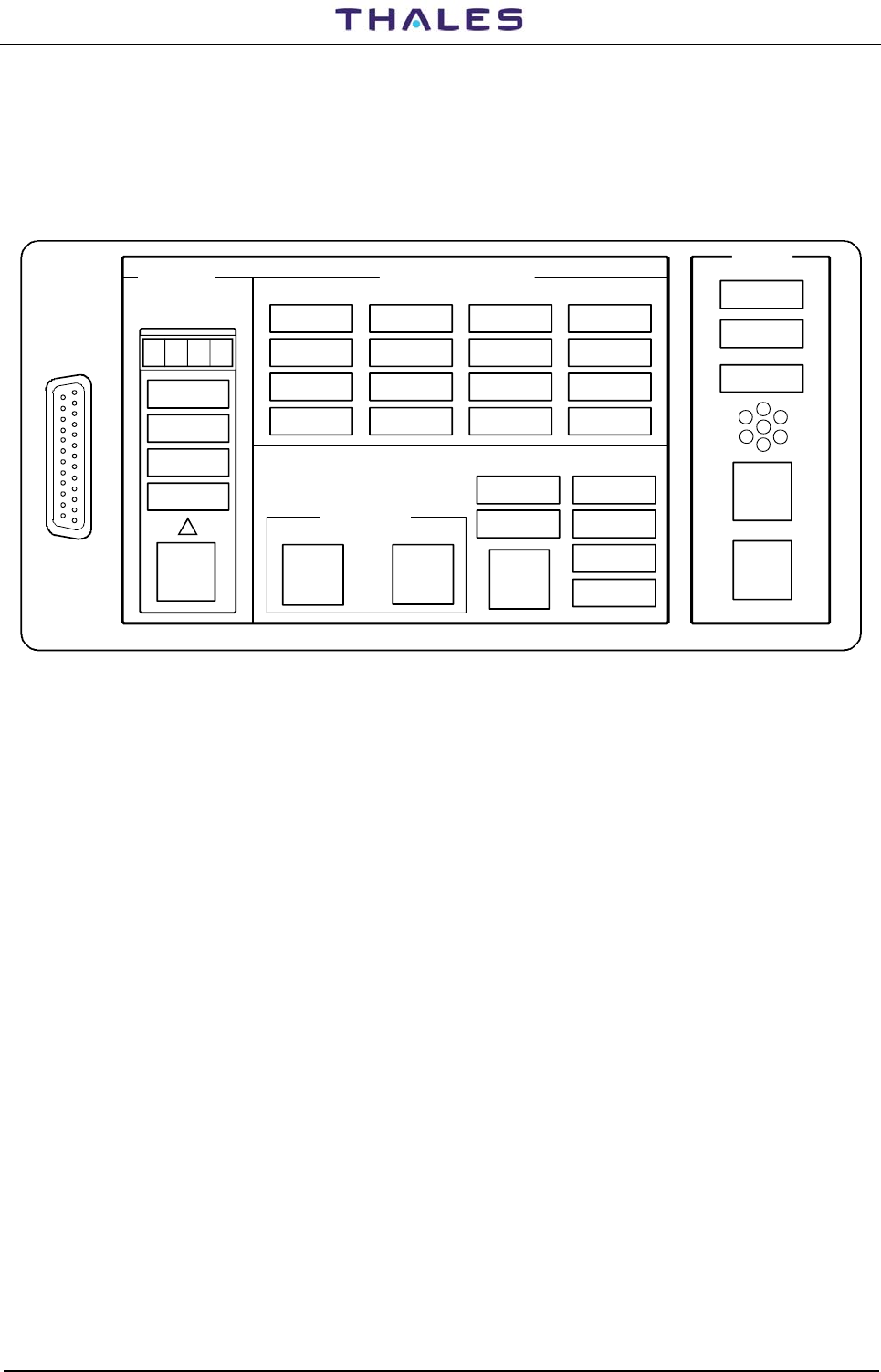
DME 415/435 -Technical Manual
Vol. 1-Section 1-General Information 955 900 031C
Vers. D, September 2005 THALES Italia S.p.A.- A. S. D. 1-45
− General indication of the faults that may occur in the equipment (OTHER WARN).
5. Beacon commands (COMMAND):
− ON/OFF button (EQUIP ON/OFF) and
− transponder on antenna change over (CHANGE OVER).
MON 1 MON 2 TX 1 TX 2
DETAILED STATUS LCSU
LOCAL CONTROL & STATUS UNIT
CONTROL STATION
ALARM
WARNING
NORMAL
DATA COM
ALARM ALARM
WARNING WARNING
WARNING
COMMAND
STBYALRM STBYALRM
ON ON
FAULTY FAULTY FAULTY FAULTY
BYPASSED BYPASSED ON ANT ON ANT
OPERATION
ENGAGED
ENABLED
MAINS OFF
ENV ALRM
ANT FTY
OTHER WARN
CHANGE
OVER
EQUIP
ON/OFF
SELECT LAMP
TEST
REQUEST
RELEASE
SIL
DATA COM
PC
RS232 RD1
RD31
RD30
RD29
RD32
RD11
RD26
RD28
RD21
RD12
RD27
RD22
RD23
RD13
RD25
RD24
RD18
RD33
RD17
RD14
RD19
RD9
RD15
RD10
RD5
RD20
RD8
RD6
RD7
RD16
RD4
S1
I6
I5
I4
I3
I2
I1
MAIN
STATUS
Figure 1.22. Local Front Panel
1.6.3.2.2.1 INDICATION AND CONTROLS - INC Module - functional description
The INC Module block diagrams are shown in figures 1.23, 1.24, 1.25.
All the electrical components are mounted on the INC module board. A transparent waterproof membrane
protects the luminous components.
The commands from I1 to I16 have a common ground and communicate with the CSB module register
through the encoder consisting in UL14a,b,c - UL15a - UL11e,f - UL8b. The program reads the coded data
by “polling” and the “debounce” is foreseen by software. The three six-bit signals (CPI 1, 2, 3) pass from
module INC connector M1 to connector M17 when module CSB is inserted.
The communication for program data exchange is through the CPA and CPD buses controlled by CSB
module registers UL10 and UL 11.
The circuits are divided into the following blocks:
Address Decoders
Circuits UL3 and UL4 generate the flip-flop chip selects and the alphanumeric display.
Brightness Control
currents are at the set value.
The brightness of the OPERATION LED-bar is controlled separately by circuits UL11a, UL12a, UL11d and
UL11a,b.
A single current peak limiter circuit (TR1 and UL3) for all the LED-bars, reduces the transient currents to
values that do not jeopardize the components.
LED-bar and driver
Flip-flops UL6, 10,13,16 each control groups of 8 LED-bars. Each LED-bar has four separate LEDs in order
to have a wide lighted surface.
The four-digit device on the alphanumeric display (RD1) is an integrated component, with its functions,
including the luminous elements, built in the chips.
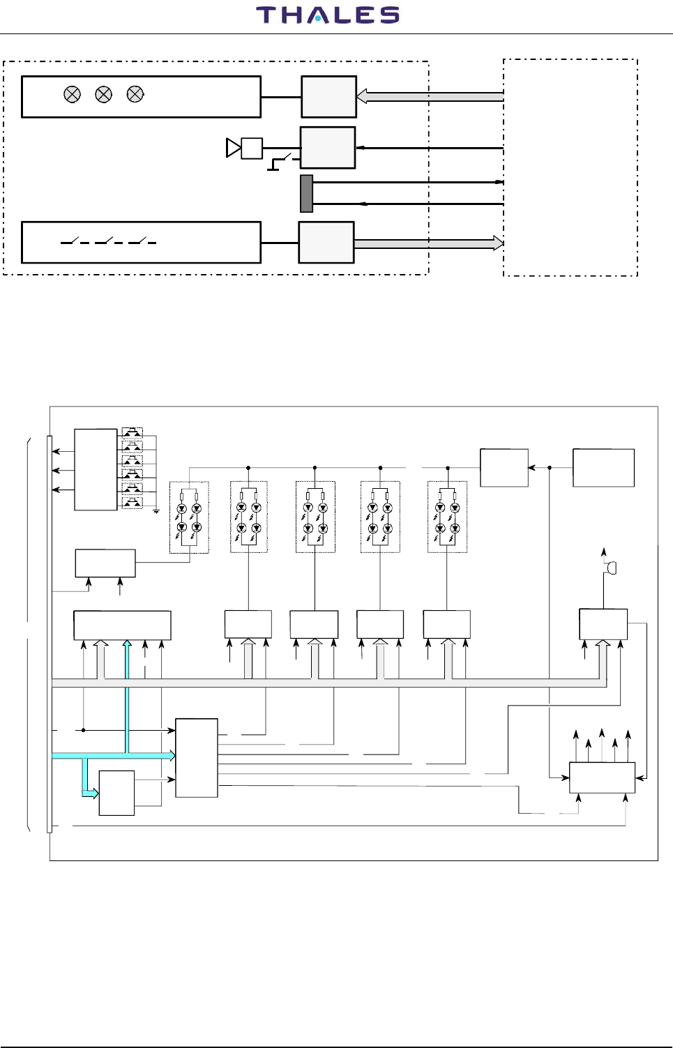
955 900 031C DME 415/435 -Technical Manual
Vol. 1-Section 1-General Information
1-46 THALES Italia S.p.A.- A. S. D. Vers. D, September 2005
key panel
Indication panel
Alarm device
display
driver
Audible
Key panel
driver
driver CSB
PC connector
local
device
Figure 1.23. INC module - simplified block diagram
Siren (Buzzer)
A siren with a fixed frequency is controlled by flip-flop UL1 and it can be silenced manually through
command 16.
CPD7
INC
CLK
D1-D8
FLIP FLOP
OC
FLIP FLOP
CLKD1-D8
FLIP FLOP
OC
FLIP FLOP
N° 1 LED BAR INRUSH
CURRENT
CIRCUIT
CLOCK
GENERATOR
N° 8 LED BAR N° 8 LED BAR N° 8 LED BAR N° 5 LED BAR
CPA BUS
CPD BUS
VLED
WDO
CPWR
To
CSB
DECODER
DECODER
BUZZER
WDO_LED
CPI1
CPI2
CPI3
I1
I2
I3
I4
I5
I6
AOA1
D0-D6 EN
4 ALPHANUMER. DISPLAY
WR
0
1
2
3
1
0
COMMAND
ENCODER
BRIGHTNESS
CLK
CLKD1-D8
FLIP FLOP
OC
5
4CONTROL
BR1
LEN1
LEN2
LEN3
LEN4
OPERATION
LEN1 LEN2 LEN3 LEN4
"LCSU OPERATION"
BRIGHTNESS
CONTROL
BR1
VCC
GND
CU.SE
EN
CLK_0
CLK_1
CLK_2
CLK_3
ENDIS1
CLK_4
CLK_5
M1
CLKD1-D8
OC CLKD1-D8
OC
Figure 1.24. INC Module - Indication and Control: General Block Diagram
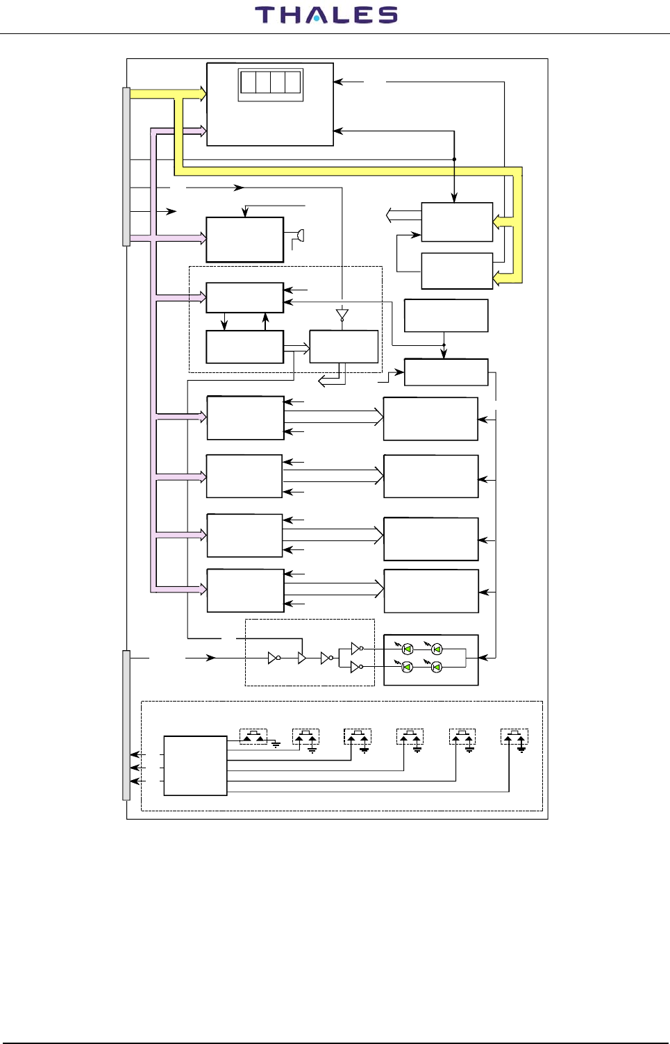
DME 415/435 -Technical Manual
Vol. 1-Section 1-General Information 955 900 031C
Vers. D, September 2005 THALES Italia S.p.A.- A. S. D. 1-47
UL1
UL5
UL7
UL6
UL4
UL3
UL2
TR1
RD1
UL10
UL13
UL16
RD 4,5,6,7,8,9,10,11
RD 12,13,14,15,17,18,19,20
RD 21,22,23,24,25,26,27,28
RD 29,30,31,32,33
RD16
Flip-Flop
LATCH S1
VCC
MUX
REGISTER
SERIAL IN-
PARALL.OUT
CLK
UL9a,b,c,d
LEN
3 STATE BUFFERS
DECODER
DECODER
N° 8 LED BAR
CLOCK GENERAT.
SQUARE OSCILLATOR
INRUSH CURR.CIRCUIT
LEN 1
LEN 2
LEN 3
LEN 4
CLK 0
CLK 1
CLK 2
CLK 3
N° 8 LED BAR
N° 8 LED BAR
N° 5 LED BAR
N° 1 LED BAR "OPERATION"
WDO_LED
0123
DPY LED
ENDIS
ALPHANUMERIC DISPLAY
UL8a
WD0
+5
VCC
M1
CPA BUS
CPD BUS
UL11a UL12a UL11d
UL11b
UL11c
CPD BUS
VCC
CPA0,1
CPD0...6
CPWR
CPA0,1,6
CPA2..5
CPD0...7
BRIGHTNESS CONTROL
Flip-Flop
LATCH
BUFFER
Flip-Flop
LATCH
BUFFER
Flip-Flop
LATCH
BUFFER
Flip-Flop
LATCH
BUFFER
BRIGHTNESS CONTROL
I1 I2 I6
I4 I5
I3
COMMAND
ENCODER
M1
CP1
CP2
CP3 UL14 a,b - UL15a
UL11 e,f - UL8b
SELECT EQUIP
ON/OFF CHANGE
OVER REQUEST
RELEASE
LAMP
TEST SIL
BR1
CLK 4
CLK 5
VLED
Figure 1.25. INC Module - Indication and Control: Block Diagram
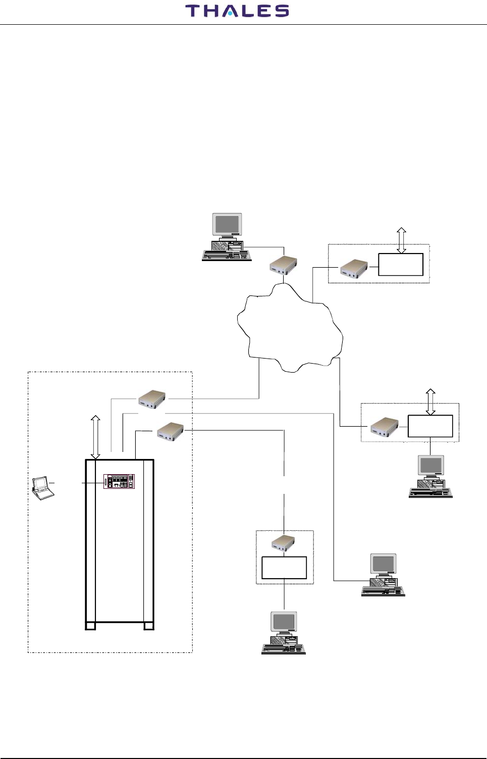
955 900 031C DME 415/435 -Technical Manual
Vol. 1-Section 1-General Information
1-48 THALES Italia S.p.A.- A. S. D. Vers. D, September 2005
1.6.3.3 REMOTE CONTROL SYSTEM
RCSI 446 or RCSE 443 – Remote Control & Status Indicator - is a unit for remote control and maintenance
operations (for detailed information to see RCSI 446 or RCSE 443 Technical manual).
An updated remote control, MCS (Monitoring and Control System), with resident software on PC, work with
modern programs that only run on hardware of a typical PC (for detailed information to make reference to the
MCS Technical manual)
The possible remote site connections with the local station are shown in figure 1.26.
The examples of remote site connections with the local station are shown in figures 1.27 and 1.28.
RCSI/SI
446 2/8
RCSI/RCSE
RCSI/RCSE
(PSTN-Public Switching
Telephon Net.)
modem
modem
modem 2
modem
PL2
PL1
PL3
SK2 SK1
RS232 A
RS232 B
optional
ON/OFF
DATA
SWITCHED
NETWORK
ON/OFF
DATA
DEDICATED
LINE
NOTE
1) RS232 line (A) UNAVAILABLE if
RS232 line (B) is used or viceversa
2) "External" MODEM 1&2 Unavailable
if "Internal" MODEM are used and viceversa
optional
ON/OFF
DATA
DME
modem1
Figure 1.26. Possible connection between Remote RCSI/RCSE and Local site
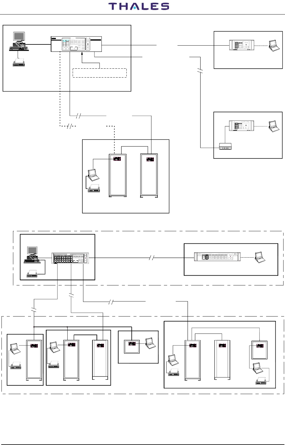
DME 415/435 -Technical Manual
Vol. 1-Section 1-General Information 955 900 031C
Vers. D, September 2005 THALES Italia S.p.A.- A. S. D. 1-49
REMOTE CONTROL STATUS INDICATOR
RCSI 446-2 STATUS INDICATOR
SI 446 - 2
RCSI 446
WAR NI N G
NORMAL
ALA R M
1
ON
SIL
LAMP
TEST
EQUIPMENT STATUS SI
WAR NING
NORMAL
ALAR M
2
RS 232
DME
(D)VOR
EQUIPMENTS LOCAL SITE
CENTER CONTROL ROOM
DEDICATED LINE
CONTROL TOWER
EQUIPMENT RCSI
12 DETAI LED STA T USMAIN ST AT US
COMMAN D
RS 232
Optional ENVIRONMENT ALARMS
(SM O KE, TEM P., INTRU S ION , ...)
STATUS INDICATOR
SI 446 - 2
WAR NI N G
NORMAL
ALA R M
1
ON
SIL
LAMP
TEST
EQUIPMENT STATUS SI
WAR NIN G
NORMAL
ALA R M
2
RS 232
Switched or dedicated teleph. LINE
Modem
PC
PC
RS 232
RS 422/485
DEDICATED
or SWITCHED LINE
RS 422 (<1km)
Figure 1.27. Example of single site connection with RCSI
STATUS INDICATOR
SI 446-8
RS 422 (< 1 Km.)
REMOTE CONTROL
& STATUS INDICATOR
RCSI 446-8
2
ALAR M
NORMAL
WARNING
TEST
LAMP SIL
ON
1
AL A R M
NORMAL
WARNING
4
AL AR M
NORMAL
WARNING
3
AL A R M
NORMAL
WARNING
6
AL AR M
NORMAL
WARNING
5
ALAR M
NORMAL
WARNING
8
AL AR M
NORMAL
WARNING
7
AL A R M
NORMAL
WARNING
EQUI PME N T ST A TU S SI
NDB 436
L2 - DEDICATED
L1 - DEDICATED LINE
RS 232
DME
(D)VOR
RS 232
DME
GP
ILS
LOC
ILS
MARKER
RS 232
SEL E CT
WARNING
NORMAL
DATA COM
ALARM
SELE CT
WARNING
NORMAL
DATA COM
ALARM
SEL E CT
WARNING
NORMAL
DATA COM
ALARM
SELE CT
WARNING
NORMAL
DATA COM
ALARM
SEL E CT
WARNING
NORMAL
DATA COM
ALARM
SELE CT
WARNING
NORMAL
DATA COM
ALARM
SEL E CT
WARNING
NORMAL
DATA COM
ALARM
SELE CT
WARNING
NORMAL
DATA COM
ALARM
EQU IPM E N T RCSI
RCSI 446
12345678
DET AI LED STATUSMAIN STATU S
REQUEST
RELEASE
MON 1
STANDBY
MON 2 TX 1
ON ANT
FAULTY
WARNING
TX 2
ON ANT
FAULTY
WARNING
OPERATION
WARNING
DATA COM
SIL
FAUL TY
BYP A SS ED
FAULTY
BYPA SS ED
OTHER WARN
ANT FT Y
ENV ALRM
MAINS OFF
ENA BL E D
ENG AG E D
STATIONCONTROL
CHANGE
OVER
EQU IP
ON/OFF
COMMAND
ST AN D BY
RS 232
REMOTE SERVICE MAINTENANCE
CONTROL TOWER
RS 232
Telephon line 1 = dedicated line connetting with Modem party-line
Telephon line 2 = dedicated or switched line used for: measurement, preset and indication, (no commands) ,
connetting with Modem. Indication are displayed on PC connecting at RCSI
Telephon line 3 = dedicated line connetting with Modem
CONTROL CENTER
EQUIPMENTS LOCAL SITES
or SWITCHED LINE
DEDICATED LINE - L3
Figure 1.28. Example of multi site connection with RCSI
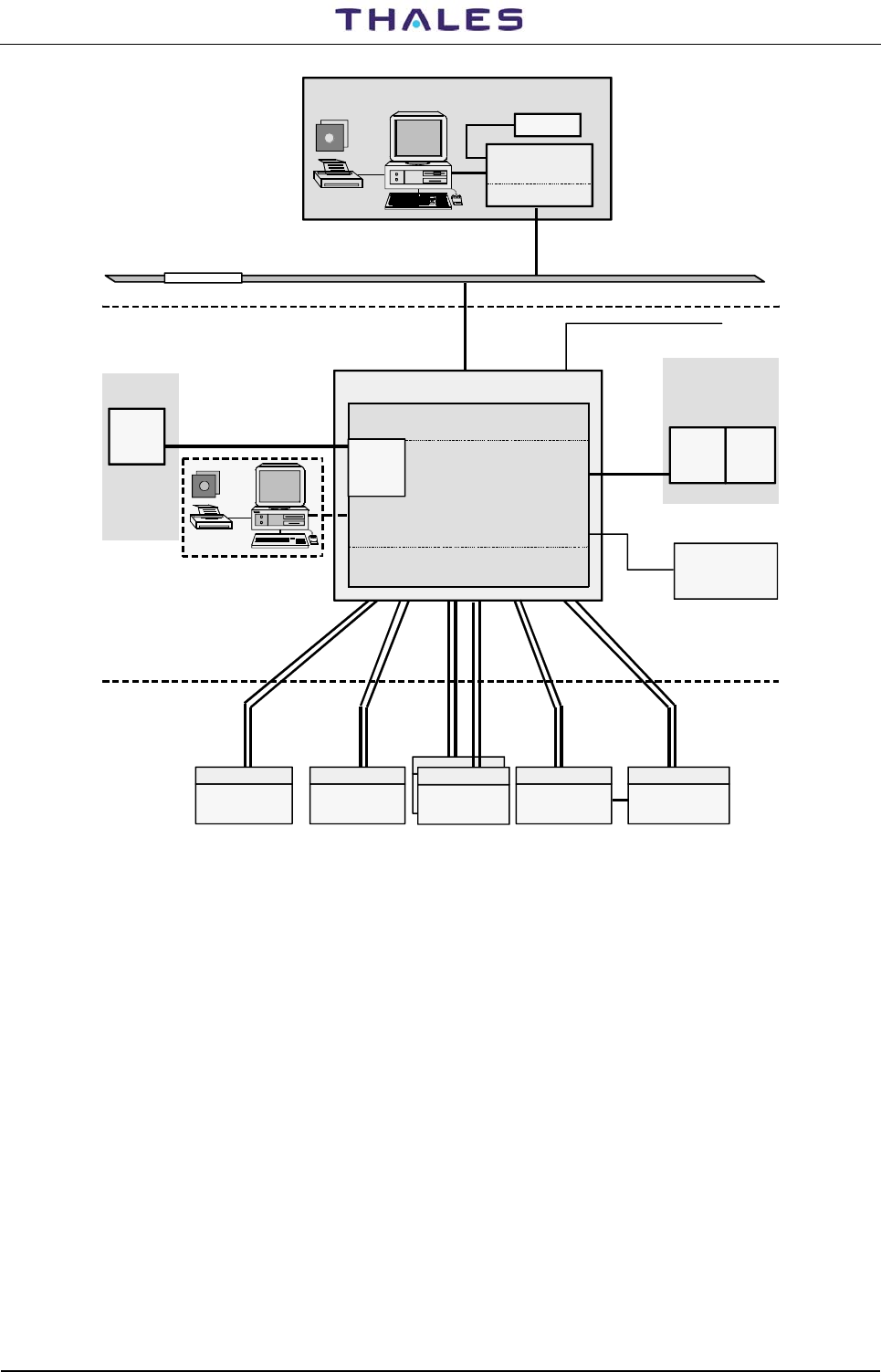
955 900 031C DME 415/435 -Technical Manual
Vol. 1-Section 1-General Information
1-50 THALES Italia S.p.A.- A. S. D. Vers. D, September 2005
MODEM
LOC
MODEM MODEM
GS
MODEM
FFM DME
RSU
CTU RWY
SELECT
TOWER
RS422*)
RS422*)
PTT LINES
RMC 443
INC
MODEM
M 4000
MODEM
Marker
MAINTENANCE CENTER
AIRPORT
RCSE 443
DIAL MODEM LGM
MODEMS LGM**)
REU
INC SIB
DIAL MODEM LGM
REU SIB
(AN 400)
*) RS422 interface to equipment situated
in a different building than RCSE -
LGM Extender 2 Unit has to be used!
**) alternatively the ILS stations can be connected
via RS232 or RS422 dedicated lines to the RCSE
(Multiplexer RS232 board is used in RCSE,
RS232 interfaces instead of ZUA modem withinILS stations)
STATIONS
Panel
Control ON/FF
(Client)
Ligne
OIO
JBUS
Figure 1.29. Example of multi site connection with RCSE
1.6.3.3.1 Remote Control & Status Indicator (RCSI 446)
The RCSI 446 is used by a remote site to control both the beacon and other equipment or devices of the
local site.
Two versions are available: RCSI 446-2 to handle up to two equipment and RCSI 446-8 to handle up to eight
equipment. Both units might be connected through dedicated lines, switched lines, radio link, etc.
Main functions of the RCSI:
- sends basic controls to the equipment (one equipment at a time; equipment(s) may also be of different
types);
- displays the status of the equipment;
- drives supplementary Status Indicators (SI 446);
- interfaces the PC to control-monitor the equipment and to perform maintenance operations like the
LCSU at the local site.
The RCSI 446-2/8 is housed in a standard 19" rack container. It comprises:
- the Control & Status Board (CSB386 module)
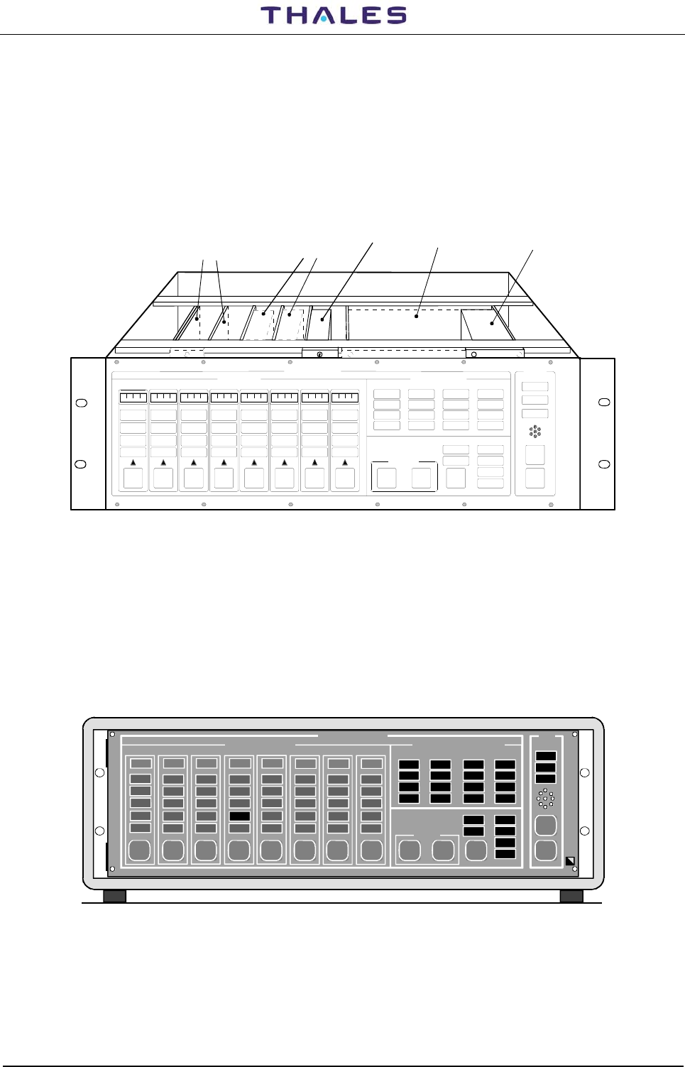
DME 415/435 -Technical Manual
Vol. 1-Section 1-General Information 955 900 031C
Vers. D, September 2005 THALES Italia S.p.A.- A. S. D. 1-51
- the front panel (made with water – proof elastic membrane) for commands and indications. The
LEDs and pushbuttons are mounted on the INC-2 or INC-8 board module. The front panel replicates
the INC module of the LCSU, plus eight status indication sections for any related equipment
- the modem(s) (optional) capable to operate with dedicated/switched lines up to 28.800 bps; up to
three modems can be housed inside the unit rack.
- the power supply (ac/dc or dc/dc alternatively).
The rack RCSI 446 - 8 is shown in Figure 1.30.
For further information, refer to the specific manual of the RCSI.
SELECT
WAR NI NG
NORMAL
DATA COM
ALARM
SELECT
WAR NI NG
NORMA L
DATA COM
ALARM
SELECT
WAR NI NG
NORMAL
DATA COM
ALARM
SELECT
WAR NI NG
NORMAL
DATA COM
ALARM
SELECT
WAR NI NG
NORMAL
DATA COM
ALARM
SELECT
WAR NI NG
NORMA L
DATA COM
ALARM
SELECT
WA RNI N G
NORMAL
DATA COM
ALARM
SELECT
WAR NI NG
NORMAL
DATA COM
ALARM
EQUIPMENT RCSI
RCSI 446
1234567
DETAILED STATUSMAIN STATUS
REQUEST
RELEASE
MON 1
STANDBY
AERIAL
MON 2 TX 1
ON ANT
FAULTY
WA RNI NG
ON
TX 2
ON A NT
FAULTY
WA RNI NG
ON
OPERATION
WA RNI NG
DATA COM
LAMP
TEST
SIL
FAULTY
BYPASSED
FAULTY
BYPASSED
OTHER WARN
ANT FTY
ENV ALRM
MAI NS OFF
ENABLED
ENGAGED
STATIONCONTROL
CHANGE
OV ER
EQUIP
ON/ OFF
COMMAN D
AERIAL
STANDBY
8
INTERFACE (OPTION) MODEM (OPTION)
MODEM 1 UPS (OPTION)
POWER SUPPLY AC/DC or DC/DC POWER SUPPLY
Figure 1.30. RCSI-8 – Remote control
1.6.3.3.2 Remote Control and Status Equipment (RCSE)
The RCSE is intended to be installed in the maintenance equipment room. It provides separate status
display and on/off-control functions for all Navaids equipment, and mechanisms to change and display
auxiliary data words for MLS. The RCSE consists of the Remote control Electronic Unit (REU) with an
Indication and Control (INC) panel. The RCSE is interfacing with one or two Control Tower Units (CTU), with
a maintenance data terminal (PC) and optionally with a slave RCSE panel unit defined as Remote Status
Unit (RSU). The CTU is intended for installation in the ATC control tower. It provides system ’main status’
indications and may provide a separate status display for each Navaids subsystem as well as switching the
ILS or MLS to the active runway (RWY-select, optional).
MAIN STATUS DETAILED STATUS
EQUIPMENT
COMMAND
RC
MON 1 MON 2 TX 1 TX 2
12 345 67 8
CONTROL STATION
ALARM
WARNING
NORMAL
DATA COM
MAINTEN
ALARM
WARNING
NOR MAL
DAT A COM
MAINTEN
ALARM
WARNING
NOR MAL
DAT A COM
MAINTEN
ALARM
WARNING
NORMAL
DATA COM
MAINTEN
ALARM
WARNING
NORMAL
DATA COM
MAINTEN
ALARM
WARNING
NORMAL
DATA COM
MAINTEN
AERIAL
STANDBY
FAULTY
BYPASSED
ON
WARNING
FAULTY
ON ANT
ON
WARNING
FAULTY
ON ANT
ENGAGED
ENABLED
MAINS OFF
ENV ALRM
ANT FTY
OTHER WARN
OPERATION
WARNING
DATA COM
ALARM
WARNING
NOR MAL
DAT A COM
MAINTEN
ALA RM
WARNING
NOR MAL
DAT A COM
MAINTEN
AERIAL
STANDBY
FAULTY
BYPASSED
SELECT SELECT SELECT SELECT SELECT SELECT SELECT SELECT EQUIP
ON/OFF CHANGE
OVER REQUEST
RELEASE LAMP
TEST
SIL
Figure 1.31. RCSE 443 – Remote control
The front RCSE 443 is shown in Figure 1.31 and CTU & Runway select , optional in figure1.32.
For further information, refer to the specific technical manual of the RCSE.
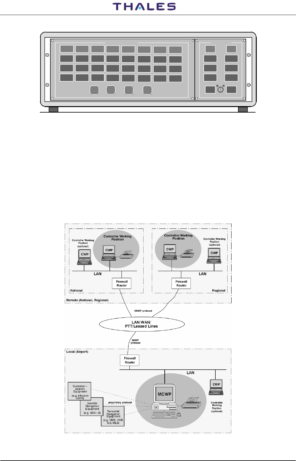
955 900 031C DME 415/435 -Technical Manual
Vol. 1-Section 1-General Information
1-52 THALES Italia S.p.A.- A. S. D. Vers. D, September 2005
Control Tower Unit (CTU) RunWaY Select
AIR NAV SUBSYSTEM RWY-SELECT
Figure 1.32. RCSE 443 – Remote control CTU & RunWay select
1.6.3.3.3 MCS
The RMMC network has a radially configured architecture based on communication between Monitoring and
Control Systems (MCS) on different levels, local (airport) and remote (regional, national, international). The
MCS systems are connected via WAN/LAN Internet or via switched/private lines in the public network (PTT)
and dedicated lines in private networks. A direct Navaids shelter access is possible via a serial or
(optionally) via an Ethernet connection.
With the use of the MCS for control and monitoring via personal computer (PC) a user-friendly interface for
the supervision adjustment and modification of relevant operating data according to the respective
operational application is made available for first set up and ongoing operation of the terrestrial and satellite
navigation equipment (e g. VOR, DME, ILS, MLS, ADS-B). The use of common PC standards and operating
systems ensures a familiar operating environment for the user (see figure 1.33).
For detailed further information, refer to the specific technical manual of the MCS.
Figure 1.33. MCS – Remote control