UBS Axcera 325A 500-Watt VHF Low-band Television Transmitter User Manual Chapter 5
UBS-Axcera 500-Watt VHF Low-band Television Transmitter Chapter 5
UserManual.wiki
>
UBS Axcera
>
325A User Manual
>
Chapter 5
Contents
1.
Title Page
2.
Table of Contents
3.
Table of Contents Tables and Figures
4.
Chapter 1
5.
Chapter 2
6.
Chapter 3
7.
Chapter 4
8.
Chapter 5
9.
Appendix A Spec Sheet
10.
Appendix B Log Sheet
11.
Appendix C Drawing
12.
Appendix C Drawing Page 1
13.
Appendix C Drawing Page 2
14.
Appendix D Drawing
Chapter 5
Navigation menu
Upload a User Manual
Namespaces
Wiki Guide
HTML
PDF
Info
Views
User Manual
Discussion / Help
Navigation
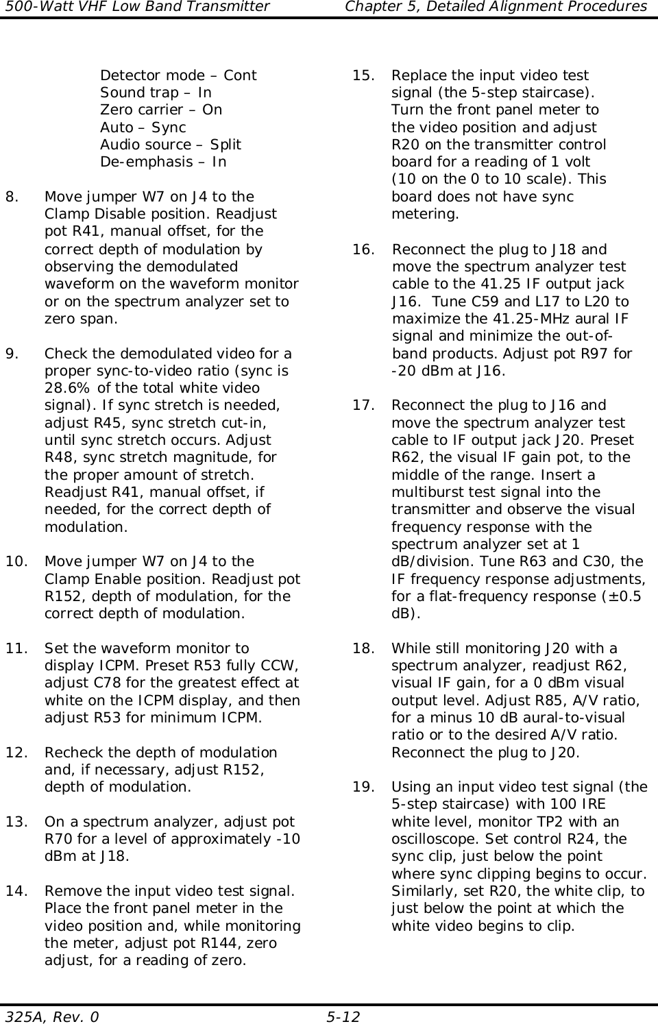
![500-Watt VHF Low Band Transmitter Chapter 5, Detailed Alignment Procedures325A, Rev. 0 5-75.11.1 (A5) AGC Control Board(1142-1601; Appendix D)Using a calibrated wattmeter, check thatthe tray is operating at the rated power.Remove the sample forward powerconnection J4 from the (A13) AGC controlboard (1142-1601). The output powerlevel should drop to 20% because of theVSWR cutback and DS4 should beilluminated. The front panel ModuleStatus LED should not be lit.Reconnect J4 and adjust R59 to begincutting back on the output power levelwhen the reflected level increases above20%.In the Power Supply Voltage position, thefront panel meter is calibrated to +48VDC using R86 on the AGC control board.5.11.2 (A1-A1) Phase Shifter Board(1198-1602; Appendix D)There are no adjustments to (A1-A1) thephase shifter board (1198-1602). Thefront panel has adjustments for phasethat are made during the amplifier arraysetup procedure.5.11.3 (A1-A2) VHF Filter/AmplifierBoard (1198-1606; Appendix D)The (A1-A2) VHF filter/amplifier board(1198-1606) has approximately 15 dB ofgain. Tune the channel filter capacitorsC29 and C20 (loading), C26 and C23(center frequency), and C24 (coupling) atJ6 on the board for the best response.Set voltage adjust pot R19 for +24 VDCat the anode of CR5.The idling current, no RF drive applied, ofthe device Q1 is set for 250 mA. To setthe current, remove the RF drive,measure the voltage across R16 (a 1Ωresistor on the filter/amplifier board) andadjust R13 for .25 volts (using Ohms’Law: [E=I x R] : [E=250 mA x 1 Ω] :E=250 mV).5.11.4 (A2-A1) Low-Band VHFAmplifier Board (1198-1605;Appendix D)The (A2-A1) VHF low-band amplifierboard (1198-1605) has 20 dB of gain andis biased for 3 amps of idling current, noRF drive applied. Adjust voltage adjustpot R10 for +24 VDC at pin 0 of theregulator IC U1. To set the bias, removethe RF drive from the board, measure thevoltage across R6 and R7 (two 1Ωresistors in parallel on the high-banddriver board), and adjust R4 for 1.5 volts(using Ohms’ Law: [E=I x R] : [E=3amps x .5 Ω] : E=1.5 volts).Connect a spectrum analyzer to outputjack J2 on the board and adjust C15 forpeak output.5.11.5 (A2-A2) Overdrive ProtectionBoard (1198-1601; Appendix D)The level of the RF input and output ofthe (A2-A2) overdrive protection board(1198-1601) should be +35 dBm duringnormal operation.To set up the overdrive circuit, check thatthe output power level of the transmitteris at 100% and adjust R11 on the boardfor a reading of .4 VDC at TP1. Increasethe output power level of the transmitterto 110%, sync only, and adjust R12 untilthe output power begins to drop off.Return the output power level of thetransmitter to 100%.5.11.6 (A2-A3) 3-Way Splitter Board(1198-1607 or 1198-1608; AppendixD)There are no tuning adjustments for (A2-A3) the 3-way splitter board. The boardtakes the +35 dBm input and splits it intothree equal +30 dBm inputs.](https://usermanual.wiki/UBS-Axcera/325A.Chapter-5/User-Guide-265277-Page-7.png)
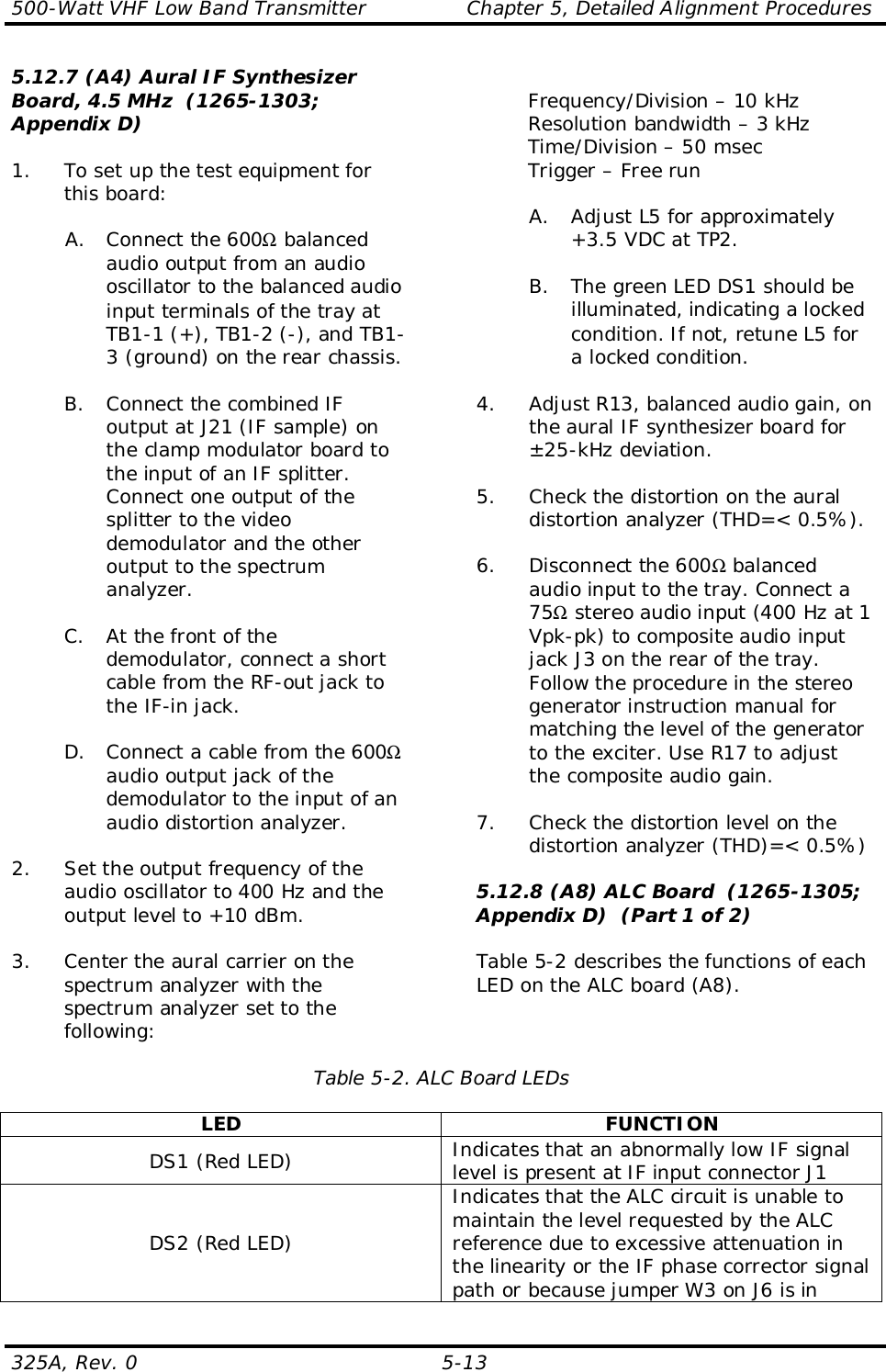
![500-Watt VHF Low Band Transmitter Chapter 5, Detailed Alignment Procedures325A, Rev. 0 5-9Switch on the tray and adjust the frontpanel meter, in the Reflected OutputPower position, to a 100% reading usingR53, the reflected power meter adjust onthe AGC control board. Adjust thereflected output power to a 20% readingusing R5 on the AGC control board.Adjust R59, the VSWR cutback adjust onthe AGC control board, until the redVSWR Cutback LED DS4 on the frontpanel lights. This sets up the VSWRcutback circuitry.Readjust R5 for 100% on the meter toachieve a 500 watts peak of sync output+ 50 watts aural power. However, if thesystem requires less output power peramplifier tray, adjust each tray by thesame amount to give the desired totaloutput power.Switch off the tray and return the J5 andJ8 cables on the 3-way combinerassembly back to their original positions.If the tray was originally operating below100% output power, the AGC fault adjustwas set for 20% below the operational %Output Power of the tray. See the TestData Sheet for the transmitter for theactual readings for the tray. Place S1 onthe AGC control board in the AGCposition. This is the normal operatingposition after the setup is completed.There is a spare 1-amp and 10-amp fuseon the top, right-hand side of the tray.These are replacements for fuses on thecurrent metering board.The VHF amplifier tray is aligned,calibrated, and ready for normaloperation.5.12 Board Level AlignmentProcedures5.12.1 (Optional) 4.5-MHzComposite Input KitIf the (optional) 4.5-MHz composite inputkit is purchased, the tray is capable ofoperating by using either the 4.5-MHzcomposite input or the baseband audioand video inputs. The kit adds the (A24)composite 4.5-MHz filter board (1227-1244; Appendix D) and the (A25) 4.5-MHz bandpass filter board (1265-1307;Appendix D) to the transmitter. When the4.5-MHz intercarrier signal generated bythe 4.5-MHz composite input has beenselected by the 4.5-MHz composite inputkit, the 4.5-MHz generated by the auralIF synthesizer board is not used. Whenthe 4.5-MHz intercarrier signal generatedby the baseband video and audio inputswith baseband has been selected by the4.5-MHz composite input kit, thecomposite 4.5-MHz filter board and the4.5-MHz bandpass filter board are notused.The tray has been factory tuned andshould not need any alignments toachieve normal operation. To align thetray for the 4.5-MHz composite input,apply the 4.5-MHz composite input, withthe test signals used as needed, to thevideo input jack (J1 or J2 [loop-throughconnections]) on the rear of the tray.Select the 4.5-MHz composite input byremoving the baseband select from J18-6and J18-7 on the rear of the tray.To align the exciter using baseband videoand audio inputs, apply the basebandvideo, with the test signals used asneeded, to the video input jack (J1 or J2[loop-through connections]) and thebaseband audio to the proper basebandaudio input on the rear of the tray. Forbalanced audio input, connect TB1-1(+),TB1-2(-), and TB1-3 (GND). Forcomposite/stereo audio, connect thecomposite audio input jack (J3 or J13[loop-through connections]) and connecta baseband select from J18-6 and J18-7on the rear of the tray.5.12.2 Delay Equalizer Board (1227-1204; Appendix D)The jumper W1 on J5 of the sync tipclamp/modulator board, if present, mustbe in the Enable position between pins 2and 3.](https://usermanual.wiki/UBS-Axcera/325A.Chapter-5/User-Guide-265277-Page-9.png)