UBS Axcera 840A 10,000-watt UHF solid state television transmitter User Manual Chapter 5
UBS-Axcera 10,000-watt UHF solid state television transmitter Chapter 5
Contents
Chapter 5

10-kW UHF Transmitter with Chapter 5, Detailed Alignment Procedures
Feedforward Drive
840A, Rev. 0 5-1
Chapter 5
Detailed Alignment Procedures
This transmitter was aligned at the
factory and should not require additional
alignments to achieve normal operation.
Before beginning the alignment
procedures, check that the RF output at
J2 of (A18) the output coupler assembly
of the transmitter is terminated into a
dummy load or is connected to the
antenna. While performing any
alignments, refer to the Test Data Sheet
for the transmitter and compare the final
readings from the factory with the
readings on each of the trays. They
should be very similar. If a reading is off
by a substantial amount, the problem is
likely to be in that tray.
5.1 (A1-A4) UHF Exciter Tray
(1063301; Appendix A)
If the (optional) 4.5-MHz composite input
kit has been purchased, the UHF exciter
tray is capable of operating using either
the 4.5-MHz composite input or the
baseband audio and video inputs. The kit
adds (A24) the composite 4.5-MHz filter
board and (A25) the 4.5-MHz bandpass
filter board to the UHF exciter. The 4.5
MHz generated by the aural IF
synthesizer board is not used when the
4.5-MHz composite input kit has selected
the 4.5-MHz intercarrier signal generated
by the 4.5-MHz composite input. The
composite 4.5-MHz filter board and the
4.5-MHz bandpass filter board are not
used when the 4.5-MHz composite input
kit uses the 4.5-MHz intercarrier signal
generated by the baseband video and
audio inputs with baseband select.
The exciter tray has been factory tuned
and should not need to be aligned to
achieve normal operation. To align the
UHF exciter for 4.5-MHz composite input,
apply the 4.5-MHz composite input, with
the test signals used as needed, to video
input jack J1 on the rear of the tray.
Select the 4.5-MHz composite input by
removing the baseband select from J7-6
and J7-7 on the rear of the tray, if
applied.
To align the UHF exciter using baseband
video and audio inputs, connect the
baseband video, with the test signals
used as needed, to video input jack J2 on
the remote interface panel. For balanced
audio input, connect the baseband audio
to TB1-1(+), TB1-2(-), and TB1-3 (GND)
on the remote interface panel. For
composite/stereo audio, connect the
stereo source to J6 on the remote
interface panel.
5.1.1 (A6) (Optional) Delay Equalizer
Board (1227-1204; Appendix B)
This board has been factory tuned and
should not be retuned without the proper
equipment. If it is necessary to tune the
board:
1. Select a sinX/X test signal as the
video source to the delay equalizer
board.
2. Monitor the video output of the
board at video sample jack J2 with
a video measuring set (VM700) that
has been adjusted to measure
group delay.
3. Tune the four stages of the board
using the variable inductors (L1-L4)
and potentiometers (R7, R12, R17,
and R22) until the signal attains the
FCC group delay curve. The stages
are arranged in order of increasing
frequency. Adjust R29 as needed to
attain the same level coming out of
the board as is going into the
board.

10-kW UHF Transmitter with Chapter 5, Detailed Alignment Procedures
Feedforward Drive
840A, Rev. 0 5-2
5.1.2 (A24) (Optional) Composite
4.5-MHz Filter Board (1227-1244;
Appendix B)
The (A24) (optional) composite 4.5-MHz
filter board will only function properly
with a 4.5-MHz composite input signal
and with the 4.5-MHz composite input
selected.
Connect the test signal from an envelope
delay measurement set to the video
input of the tray at J1 or J2.
Connect an oscilloscope to jack J7, video
out, between the J7 center pin and pin 1
or 3 ground. Adjust C21, frequency
response, if needed, for the best
frequency response. Adjust R32, video
gain, for a signal level of 1 Vpk-pk on the
oscilloscope.
The output at J6 and J7 of the board
should be video only with no 4.5-MHz
aural subcarrier.
5.1.3 (A25) (Optional) 4.5-MHz
Bandpass Filter Board (1265-1307;
Appendix B)
The (A25) (optional) 4.5-MHz bandpass
filter board will only function properly
with a 4.5-MHz composite input signal
and with the 4.5-MHz composite input
selected.
Adjust the filter with L2, C3, L4, and C7
for a frequency response of no greater
than ±.3 dB from 4.4 to 4.6 MHz.
Adjust C19 for an overall peak-to-peak
variation of less than ±.3 dB from 4.4
MHz to 4.6 MHz.
Recheck the frequency response; it may
have changed with the adjustment of the
envelope delay. If necessary, retune the
board.
5.1.4 (A7) IF Carrier Oscillator Board
(1191-1404; Appendix B)
To align (A7) the IF carrier oscillator
board:
1. While monitoring J3 with a
spectrum analyzer, observe the
45.75-MHz visual IF (typical +5
dBm).
2. Connect a frequency counter to J3
and adjust C17 for 45.750000 MHz.
3. Connect a frequency counter to J1
and check for 50 kHz; this is the
aural phase lock loop (PLL)
reference.
5.1.5 (A5) Sync Tip Clamp/
Modulator Board (1265-1302;
Appendix B)
To align (A5) the sync tip clamp/
modulator board:
1. Determine if jumper W4 on jack J3
is present. Jumper W4 terminates
the video input into 75Ω. Remove
jumper W4 if the video loop-
through is required on the rear
chassis at jacks J1 and J2.
2. Set the controls R20, the white clip,
R24, the sync clip, and R45, the
sync stretch cut-in, to their fully
counter-clockwise (CCW) position.
Set R48, the sync magnitude, fully
clockwise (CW).
3. Place the jumper W7 on jack J4 to
the clamp off, disable, position.
4. Connect a 5-step staircase video
test signal to the input of the
transmitter.
5. Monitor TP2 with an oscilloscope.
Adjust R12, the video gain pot, for
1 Vpk-pk.
6. Change the video input test signal
to a multiburst test pattern. While

10-kW UHF Transmitter with Chapter 5, Detailed Alignment Procedures
Feedforward Drive
840A, Rev. 0 5-3
monitoring TP2, adjust C8 and R32
for a flat-frequency response.
Change the input video test signal
back to the 5-step staircase.
7. Monitor TP2 with an oscilloscope.
Adjust the pot R41, manual offset,
for a blanking level of -0.8 VDC.
The waveform in Figure 5-1 should
be observed at this point. Move
jumper W2 on J4 to the clamp
enable position. Adjust pot R152,
depth of modulation, for a blanking
level of -0.8 VDC.
0
V
o
lt
s
.1 Volts
Figure 5-1. Waveform at TP2.
Note: The waveform in Figure 5-1
represents the theoretical level for
proper modulation depth. Step 9
below describes how to set the
modulation depth through the use of
a television demodulator or a zero-
spanned spectrum analyzer tuned to
the visual IF frequency.
8. The following test setup is for the
adjustment of the depth of
modulation and ICPM at IF:
A. Remove the cable that is now
on J18. Connect the double
sideband 45.75-MHz visual IF
signal from J18 to a 10-dB
splitter/coupler. Connect the
coupled port of the splitter/
coupler to the RF input of a
television demodulator.
Connect the direct port to a
spectrum analyzer.
B. Connect the 75-Ω video output
of the demodulator to the video
input of a waveform monitor.
For incidental carrier phase
modulation (ICPM)
measurements, also connect
the quadrature output of the
demodulator to the horizontal
input of the waveform monitor
using a 250-kHz low-pass filter.
(An oscilloscope can be used in
place of a waveform monitor).
C. Set the controls of the
demodulator as follows:
• Detector Mode: Cont
• Sound Trap: In
• Zero Carrier: On
• Auto: Sync
• Audio Source: Split
• De-Emphasis: In
9. Move jumper W7 on J4 to the clamp
disable position. Readjust pot R41,
manual offset, for the correct depth
of modulation by observing the
demodulated waveform on the
waveform monitor or on the
spectrum analyzer set to zero span.
10. Check the demodulated video for
the proper sync-to-video ratio (sync
is 28.6% of the total white video

10-kW UHF Transmitter with Chapter 5, Detailed Alignment Procedures
Feedforward Drive
840A, Rev. 0 5-4
signal). If sync stretch is needed,
adjust R45, sync stretch cut-in,
until sync stretch occurs. Adjust
R48, sync stretch magnitude, for
the proper amount of stretch.
Readjust R41, manual offset, if
necessary, for the correct depth of
modulation.
11. Move jumper W7 on J4 to the clamp
enable position. Readjust pot R152,
the depth of modulation, for the
correct depth of modulation.
12. Set the waveform monitor to
display ICPM. Preset R53 fully CCW,
adjust C78 for the greatest effect at
white on the ICPM display, and
adjust R53 for minimum ICPM.
13. Recheck the depth of modulation
and, if necessary, adjust R152,
depth of modulation.
14. Adjust pot R70 for a level of
approximately -10 dBm on the
spectrum analyzer at J18.
15. Remove the video input. Place the
front panel meter in the video
position and, while monitoring the
meter, adjust pot R144, zero
adjust, for a reading of zero.
16. Replace the video input test
signal (the 5-step staircase).
Turn the front panel meter to
the Video position and adjust
R20 on the transmitter control
board for a reading of 100 (10
on the 0-to-10 scale). This
board does not have sync
metering.
17. Reconnect the plug to J18 and
move the spectrum analyzer test
cable to 41.25 IF output jack J16.
Tune C59 and L17-L20 to maximize
the 41.25-MHz aural IF signal and
minimize the out-of-band products.
Adjust pot R97 for -20 dBm at J16.
18. Reconnect the plug to J16 and
move the spectrum analyzer test
cable to IF output jack J20. Preset
R62, the visual IF gain pot, to the
middle. Insert a multiburst test
signal into the transmitter and
observe the visual frequency
response with the spectrum
analyzer set at 1 dB/division. Tune
R63 and C30, the IF frequency
response adjustments, for a flat-
frequency response (±0.5 dB).
19. While still monitoring J20 with a
spectrum analyzer, readjust R62,
visual IF gain, for a visual output
level of 0 dBm. Adjust R85, A/V
ratio, for a -10 dB aural-to-visual
ratio or to the needed A/V ratio.
Reconnect the plug to J20.
20. Using an input video test signal (the
5-step staircase) with a 100 IRE
white level, monitor TP2 with an
oscilloscope. Set the control R24,
the sync clip, just below the point
where sync clipping begins to occur.
Also, set R20, the white clip, to the
point just below where the white
video begins to clip.
Note: This procedure should be
performed after the system setup or
if linearity problems occur.
5.1.6 (A26) Diacrode VSBF Bypass
Board (1293-1230; Appendix B)
The (A26) diacrode VSBF bypass board is
used to bypass the clamp board saw filter
when S1 and S2 are in the enable
position. This double sideband signal can
be used to sweep the tube cavity with a
double sideband and no aural present. C2
is used to flatten the double sideband
response. S1 and S2 are normally in the
bypass position.

10-kW UHF Transmitter with Chapter 5, Detailed Alignment Procedures
Feedforward Drive
840A, Rev. 0 5-5
5.1.7 (A4) Aural IF Synthesizer
Board, 4.5 MHz (1265-1303,
Appendix B)
1. The test equipment setup for (A4)
the aural IF synthesizer board, 4.5
MHz, is as follows:
A. Connect a 600-Ω balanced
audio output from an audio
oscillator to the balanced audio
input terminals of the tray at
TB1-1 (+), TB1-2 (-), and TB1-
3 (ground) on the rear chassis.
B. Connect the combined IF
output at J21, the IF sample on
the clamp modulator board, to
the input of an IF splitter.
Connect one output of the
splitter to the video
demodulator and the other
output to the spectrum
analyzer.
C. Connect a short cable at the
front of the demodulator from
the RF-out jack to the IF-in
jack.
D. Connect a cable from the 600-
Ω audio output jack of the
demodulator to the input of an
audio distortion analyzer.
2. Set the output frequency of the
audio oscillator to 400 Hz and the
output level to +10 dBm.
3. Center the aural carrier on the
spectrum analyzer with the
spectrum analyzer set to the
following:
• Frequency/Division: 10 kHz
• Resolution Bandwidth: 3 kHz
• Time/Division: 50 msec
• Trigger: Free run
A. Adjust L5 for approximately
+3.5 VDC at TP2.
B. The green LED DS1 should be
illuminated, indicating a locked
condition. If not, retune L5 for
a locked condition.
4. Adjust R13, balanced audio gain, on
the aural IF synthesizer board for
±25 kHz deviation.
5. Check the distortion on the aural
distortion analyzer (< 0.5%).
6. Disconnect the 600-Ω balanced
audio input to the tray. Connect a
75-Ω stereo audio input (400 Hz at
1 Vpk-pk) to composite audio input
jack J3 on the rear of the tray.
Follow the procedure in the stereo
generator instruction manual for
matching the level of the generator
to the exciter. R17 is used to adjust
the composite audio gain.
7. Check the distortion level on the
distortion analyzer (< 0.5%).
5.1.8 (A8) ALC Board (1265-1305;
Appendix B) (Part 1 of 2)
The following details the meaning of each
LED of (A8) the ALC board when it is
illuminated:
• DS1 - Red LED: Indicates that an
abnormally low IF signal level is
present at IF input connector J1
• DS2 - Red LED: Indicates that the
ALC circuit is unable to maintain the
signal level requested by the ALC
reference; this is usually due to
excessive attenuation in the linearity
or the IF phase corrector signal path,
or because the jumper W3 on J6 is in
manual gain
• DS3 - Red LED: Indicates a video loss
fault
• DS4 - Red LED: Indicates that a Mute
command is present (not used in this
configuration)

10-kW UHF Transmitter with Chapter 5, Detailed Alignment Procedures
Feedforward Drive
840A, Rev. 0 5-6
• DS5 - Green LED: Indicates that the
output from the modulator is selected
as the input to the ALC board
1. To align the ALC board, preset the
following controls in the UHF exciter
tray:
• ALC board – Move jumper W1 on J4
to disable, between pins 2 and 3 (to
disable linearity correctors); move
jumper W3 on J6 to manual, between
pins 2 and 3 (for manual gain
control); adjust R87, the manual gain
pot, to mid-range
• IF phase corrector board – Move
jumper W2 on J9 to the phase
correction enable position; move the
jumper W3 on J10 to the amplitude
correction disable position.
2. The combined IF output of the sync
tip clamp modulator board is cabled
to jack J32 of the ALC board.
Remove J32 from the board and
check to see that DS1, Input Fault,
is illuminated. Reconnect J32 and
check to see that DS1 is
extinguished.
3. Jumper W3 on J6 should be in the
manual position; monitor jack J3
with a spectrum analyzer.
4. With a multiburst video signal
present, tune C4 for a flat-
frequency response of ±0.5 dB.
5. Before proceeding with part 2 of the
ALC board alignment (described in
section 5.1.10), check the IF phase
corrector board to make sure that it
is functioning properly.
5.1.9 (A9) IF Phase Corrector Board
(1227-1250; Appendix B)
Refer to the system alignment
procedures at the end of this chapter for
the set up of (A9) the IF phase corrector
board in the exciter tray. The signal level
into the board should be approximately
the same as the output of the board.
The IF input jack of the IF phase
corrector board is fed from J3, the IF
output jack of (A8) the ALC board.
The IF output jack of the IF phase
corrector board is fed to J7, the IF input
jack of (A8) the ALC board.
5.1.10 (A8) ALC Board, NTSC (1265-
1305; Appendix B) (Part 2 of 2)
Input a multiburst video test signal at the
baseband video input. Connect a
spectrum analyzer to J11. Tune C63 for a
flat-frequency response of ±0.5 dB.
Move the Operate/Standby switch on the
front panel of the transmitter to the
Operate position.
Place jumper W3 on jack J6 in the
Manual mode and adjust R87 for 0.8
volts at TP4.
Place jumper W3 on J6 in the Auto mode
and adjust the front panel power adjust
control A20 fully CW. If the optional
remote power raise/lower kit is present,
adjust switch S1 on the board to
maximum voltage at TP4. Adjust R74,
the range adjust, for 1 volt at TP4.
Adjust the front panel power adjust
control (A20) for 0.8 VDC at TP4. If the
optional remote power raise/lower kit is
present, adjust switch S1 on the board to
the mid-range of its travel and then
adjust the front panel Power Adjust
control (A20) for 0.8 VDC at TP4.
Disconnect the plug that is now on J12
(IF output) and monitor the output with a
spectrum analyzer. The output should be
approximately 0 dBm. Adjust R99, if
necessary, to increase the output level. If
a smaller output level is needed, move
the jumpers J27 and J28 to pins 2 and 3
and adjust R99 as needed. Reconnect
J12.

10-kW UHF Transmitter with Chapter 5, Detailed Alignment Procedures
Feedforward Drive
840A, Rev. 0 5-7
Move W2 on J5 to the cutback enable
position. Remove the input video signal
and verify that the output of the
transmitter drops to 25%. Adjust R71,
the cutback level, if necessary. Restore
the video input signal.
Note: This step affects the response
of the entire transmitter. Connect a
video sweep signal to the input of
the tray. Monitor the output of the
system with a spectrum analyzer.
Adjust C71 with R103 and C72 with
R106, as needed, to flatten the
response. C71 and C72 can be
adjusted for the frequency of the
correction notch being applied to the
visual response of the transmitter.
R103 and R106 are used to adjust
the depth and width of the correction
notch.
Controls R13, R18, and R23, the
magnitude controls, should be set fully
CW. Controls R34, R37, and R40 are the
linearity cut-in adjustments.
5.1.11 (A11) UHF Upconverter Board
(1265-1310; Appendix B)
To align (A11) the UHF upconverter
board, place W1 on J10 in the Manual
position. R10 is a gain control that is
adjusted to give an output of
approximately +17 dBm at J5 of the
board with an input of 0 dBm of IF.
5.1.12 (A14-A1) Channel Oscillator
Board (1145-1201; Appendix B)
The (A14-A1) channel oscillator board is
mounted in (A14) the channel oscillator
assembly. To align this board:
1. Connect J1, the main output of the
channel oscillator, to a spectrum
analyzer tuned to the crystal
frequency. Peak the tuning
capacitors C6 and C18 for
maximum output. Tune L2 and L4
for maximum output. The output
level should be about +5 dBm. The
channel oscillator should maintain
an oven temperature of 50° C.
If a spectrum analyzer is not
available, connect a digital
voltmeter (DVM) to TP1 on the x8
multiplier board. Tune capacitors C6
and C18 for maximum voltage and
tune L2 and L4 for maximum
voltage output at TP1.
2. Connect J2, the sample output of
the channel oscillator, to a suitable
counter and tune C11, coarse
adjust, to the crystal frequency.
Tune C9 for the fine-frequency
adjustment.
Caution: Do not repeak C6, C18, L2,
or L4. This can change the output
level.
Note: While adjusting C9 and C11 to
the crystal frequency, the peak
voltage monitored at TP1 of the x8
multiplier board should not decrease.
If a decrease does occur, there may
be a problem with the crystal.
Contact the ADC Field Service
Department for further instructions.
Note: If the channel oscillator in the
channel oscillator assembly is used,
the C9 fine-frequency adjust is not
on the channel oscillator board. It
can be found on the FSK
w/EEPROM board by using R9.
3. Reconnect J1, the main output of
the channel oscillator, to J1, the
input of the x8 multiplier.
5.1.13 (A15-A1) x8 Multiplier Board
(1227-1002; Appendix B)
The (A15-A1) x8 multiplier board is
mounted in an x8 multiplier enclosure
assembly. During normal operation, the
green LED DS1, which can be seen
through the access hole in the enclosure
assembly, will be lit to indicate that the
LO is present at the output of the x8
multiplier board.

10-kW UHF Transmitter with Chapter 5, Detailed Alignment Procedures
Feedforward Drive
840A, Rev. 0 5-8
Connect a spectrum analyzer to
output jack J2 of the board.
Tune C4, C6, C10, C12, C18, and C20 for
maximum output.
Readjust all of the capacitors to minimize
the seventh and the ninth harmonics of
the channel oscillator frequency. They
should be at least -30 dB down without
affecting the x8 multiplier output.
If a spectrum analyzer is not available, a
DC voltmeter can be used. When a
voltmeter is used, the harmonic
frequencies must be minimized to
prevent interference with other channels.
While monitoring each test point with a
DC voltmeter, maximize each test point
by tuning the broadband multipliers in
the following sequence:
• Monitor TP1 with a DVM and tune C4
for maximum (typical 0.6 VDC).
• Monitor TP2 and tune C6 and C10 for
maximum (typical 1.2 VDC).
• Monitor TP3 and tune C12 and C18
for maximum (typical 2.0 VDC).
• Monitor TP4 and tune C20 for
maximum.
• Repeak C12 and C10 while
monitoring TP4 (typical 3.5 VDC).
• The typical output level is +15 dBm.
5.1.14 (A19) Visual/Aural Metering
Board (1265-1309; Appendix B)
The (A19) visual/aural metering board is
adjusted to give a peak-detected output
indication to the front panel meter for the
visual output and aural output of the
driver cabinet. The board should not
need to be adjusted to achieve normal
operation.
5.1.15 (A3) +12 VDC (4A)/-12 VDC
(1A) Power Supply Board (1265-
1312; Appendix B)
There are no adjustments that need to
be made to (A3) the +12 VDC (4A)/-12
VDC (1A) power supply board. DS1 will
be lit if a +12 VDC output is connected to
J6. DS2 will be lit if a +12 VDC output is
connected to J3. DS3 will be lit if a +12
VDC output is connected to J4. DS4 will
be lit if a +12 VDC output is connected to
J5. DS5 will be lit if a -12 VDC output is
connected to J7 and J8.
5.1.16 Transmitter Control Board
(1293-1221; Appendix B)
To align the VSWR cutback, adjust the 3-
watt amplifier tray for a 12.5% Visual
Power reading on the metering control
panel. Reverse the J6 and J3 cables on
(A2-A2) the coupler on the output of the
diacrode cavity. Adjust R22 unto the
VSWR light starts to illuminate on the
exciter front panel. Place the J3 and J6
cables back in their original positions.
To align the video metering, insert a
composite or some other 100-IRE test
signal into the exciter tray. Adjust R20
for a full-scale reading (1 volt) on the
bottom scale of the front panel meter of
the exciter tray in the video metering
position.
To align the audio metering, adjust the
audio input level for a ±25 kHz deviation
using a spectrum analyzer. Adjust R19 on
the board for a 25-kHz reading on the
bottom scale of the front panel meter of
the exciter tray.
This completes the detailed alignment
procedures for the UHF exciter tray.

10-kW UHF Transmitter with Chapter 5, Detailed Alignment Procedures
Feedforward Drive
840A, Rev. 0 5-9
5.2 (A9) 3-Watt Amplifier Tray
(1068203; Appendix A)
The 3-watt amplifier tray has been
aligned at the factory and should not
require any further adjustments. If an
alignment is necessary, terminate the 3-
watt tray into a dummy load before
performing any adjustments.
5.2.1 (A1) UHF Filter (1007-1101;
Appendix B)
The (A1) UHF filter (1007-1101) has
been factory swept and should not be
tuned without the proper equipment. The
filtered output is sent to (A2) the AGC
board input jack J1.
5.2.2 (A2) AGC Board (1007-1201;
Appendix B)
Perform the following steps to align (A2)
the AGC board (1007-1201):
1. With S1 on the AGC board in the
Manual position, adjust R32 for about
a -2 dBm output at J2.
2. The RF output of the AGC board is fed
to (A27) the UHF phase shifter board
input jack J1.
5.2.3 (A27) UHF Phase Shifter Board
(1142-1315; Appendix B)
The (A27) UHF phase shifter board
(1142-1315) adjusts the phase of the
signal to produce the maximum output of
the transmitter when the two parallel
amplifiers are added together.
Adjust R7 on the front panel of the tray
for maximum output power. Monitor the
combined % Output power on the front
panel meter of the transmitter.
The phase-corrected RF output is fed to
(A3) the UHF amplifier/regulator board
input jack J1.
5.2.4 (A3) UHF Amplifier/Regulator
Board (1007-1204; Appendix B)
The (A3) UHF amplifier/regulator board
(1007-1204) has no tuning adjustments
and has a gain of about +17 dB. The
output is fed to (A5) the 3-watt amplifier
board #1 input jack J1.
5.2.5 (A5) 3-Watt Amplifier # 1
(1007-1211; Appendix B)
The (A5) 3-watt amplifier #1 (1007-
1211) has a gain of about 9 dB and is
tuned with C2, C4, and C8 for maximum
output.
The operating current, static current with
no drive applied, of the amplifier is set to
800 milliamps with R7 on (A6) the opto-
bias board. The current is determined by
measuring the voltage drop across R3,
the 3.3-ohm resistor in the collector
circuit of Q1 on the amplifier board, and
adjusting R7 for a voltage drop of 2.64
volts.
The RF output is fed to (A7) the 3-watt
amplifier board #2.
5.2.6 (A7) 3-Watt Amplifier # 2
(1007-1211; Appendix B)
The (A7) 3-watt amplifier #2 (1007-
1211) has a gain of about 9 dB and is
tuned with C2, C4, and C8 for maximum
output.
The operating current of the amplifier is
set to 850 mA with R7 on (A8) the opto-
bias board. The current is determined by
measuring the voltage drop across R3,
the 3.3-ohm resistor in the collector
circuit of Q1 on the amplifier board, and
adjusting R7 for a voltage drop of 2.8
volts.
The output of the amplifier is fed through
(A9) the UHF dual coupler assembly to
RF output jack J2 of the tray. A forward
and reflected power sample is taken from
the UHF dual coupler assembly and fed to
(A10) the dual peak detector board.

10-kW UHF Transmitter with Chapter 5, Detailed Alignment Procedures
Feedforward Drive
840A, Rev. 0 5-10
5.2.7 (A10) Dual Peak Detector
Board (1002-1208; Appendix B)
While monitoring the RF output of (A10)
the dual peak detector board (1002-
1208), adjust R32 on (A2) the AGC board
for a reading of 3-watts peak envelope
power (3 watts CW). While in the Output
position of the Meter Selector switch,
adjust R14 on the dual peak detector
board for a reading of 100% on the front
panel meter.
Move the cable from J1 of the dual peak
detector board to J2. Move the Meter
Selector switch to the Reflected Power
position and adjust R16 on the dual peak
detector board for a reading of 100%.
Replace the cable onto J1.
5.2.8 (A2) AGC Board (1007-1201;
Appendix B)
Remove RF input J1 to (A2) the AGC
board (1007-1201) and adjust R10 for a
reading of 0 volts on TP1. Replace the RF
input. The nominal reading at TP1 should
be +.35 volts.
If necessary, adjust R32 for an output
power reading of 100%. Switch S1 to the
AGC position and adjust R49 for a
reading of 100% on the Output Power
meter.
5.2.9 (A25) AGC Control Board
(1137-1201; Appendix B)
To align (A25) the AGC control board
(1137-1201), measure TP3 with a DVM
and adjust R3, gain #1, for a 0.9 volt
nominal reading. Then, if the outer loop
AGC is used, adjust R12, gain #2, for 1
volt, with the output of the transmitter at
the normal output level.
5.2.10 (A29) Overdrive Protection
Board (1142-1626; Appendix B)
To set up the override circuit, check that
the output power level of the transmitter
is at 100% with a sync-only 0 IRE test
signal. Adjust R11 for a reading of .4
VDC at TP1.
Increase the output power level of the
transmitter to 110% and adjust R12 until
the output power begins to drop off.
Return the output power level of the
transmitter to 100%. The trip circuit may
need to be readjusted if the amplifier
tray is terminated into a different load.
5.2.11 (A11) Power Supply Control
Board (1007-1202; Appendix B)
There are no adjustments to (A11) the
power supply control board (1007-1202).
5.2.12 (A22) ±12V Power Supply
Board (1062-1013; Appendix B)
There are no adjustments to (A22) the
±12V power supply board (1062-1013).
5.2.13 (A16) +24V Power Supply
Board (1007-1207; Appendix B)
To adjust the power supply for
overvoltage protection, start by
presetting R11 on (A16) the +24V power
supply board (1007-1207) fully CW.
Measure the voltage at J1-10 with a DVM
and adjust R8 for 25 volts. Adjust R11
CCW until the power supply shuts off due
to overvoltage. Adjust R8 fully CCW. Turn
off the tray, wait a few seconds, and then
turn the tray back on. This will reset the
power supply board.
While monitoring J1-10, slowly adjust R8
CW toward 25 volts. If the power supply
does not shut off at 25 volts, adjust R11
slightly more CCW until it does shut off.
Adjust R8 CCW. Reset the tray by turning
the tray off, waiting a few seconds, and
then turning the tray back on. Adjust R8
CW while monitoring J1-10 and check to
see if the supply will now shut off at 25
volts. If necessary, repeat this procedure.
Adjust the output voltage of the board at
J1-10 to 24 volts using adjustable
resistor R8.

10-kW UHF Transmitter with Chapter 5, Detailed Alignment Procedures
Feedforward Drive
840A, Rev. 0 5-11
This completes the detailed alignment
procedures for the 3-watt UHF amplifier
tray.
5.3 (A6, A7) 250-Watt Amplifier Tray
(1044027/1044028/1044029;
Appendix A)
This tray has been adjusted at the
factory to meet all specifications,
including feedforward correction, and
should not require any adjustments to
attain normal operation.
5.3.1 (A1-A1) Single Stage Amplifier
Assembly, Class A (1286-1608/
1286-1609/1286-1610; Appendix B)
The (A1-A1) single stage amplifier
assembly, class A, is made from a
generic single stage amplifier board,
class A, with a frequency determining kit.
This board operates class A and has a
gain of approximately 11 dB. The bias of
the transistor is set by the on-board
biasing circuit. Adjust R6 for 5 amps of
idle current and no RF drive applied.
Connect a voltage meter across E2 and
E3 on (A15) the amplifier protection
board and switch S1 to the #1 position.
Adjust R6 for a reading of 50 mV.
Connect a sweep test signal to J1, the RF
input jack of the UHF amplifier tray, and
monitor the output of the board at J2
with a padded-input spectrum analyzer.
Tune capacitor C5 for peak output and
tune C6 for peak output power with a
flat-frequency response at J2.
5.3.2 (A1-A3) Stripline Coupler
Board (1286-1604; Appendix B)
There are no adjustments to (A1-A3) the
stripline coupler board.
5.3.3 (A1-A5) Single Stage Amplifier
Assembly, Class AB (1286-1605/
1286-1606/1286-1607; Appendix B)
The (A1-A5) single stage amplifier
assembly, class AB, is made from a
generic single stage amplifier board,
class AB, with a frequency determining
kit.
This board operates class AB and has a
gain of approximately 9 dB. The bias of
the transistor is set by the on-board
biasing circuit. Adjust R106 for 500
milliamps and no RF drive applied.
Connect a voltage meter across E2 and
E3 on the amplifier protection board and
switch S1 to the #2 position. Adjust
R106 for a reading of 5.0 mV. Connect a
sweep test signal to J1, the RF input jack
of the UHF amplifier tray, and monitor
the output of the board at J2 with a
padded-input spectrum analyzer. Tune
capacitor C105 for peak output and tune
C119 for peak output with a flat-
frequency response and minimum
current at J2.
5.3.4 (A19-A6) 2-Way Splitter
Assembly
There are no adjustments to (A19-A6)
the 2-way splitter assembly (1044096).
5.3.5 (A19-A7, A19-A8) Dual Output
Power Amplifier Assemblies, Class
AB (1286-1316/1286-1317/1286-
1318; Appendix B)
Each board in (A19-A7, A19-A8) the dual
output power amplifier assemblies, class
AB, is made from a generic dual stage
amplifier board, class AB, with a
frequency determining kit.
These boards operate class AB and have
a gain of approximately 9 dB. The idling
current for each of the transistors is set
to 250 mA.
To adjust the idling currents, no RF
applied to the tray, of the devices on
(A1-A7), connect a voltage meter across
E2 and E3 on the amplifier protection
board. Switch S1 to the #3 position and
adjust R106 for a reading of 2.5 mV.
Switch S1 to the #4 position and adjust
R206 for a reading of 2.5 mV.

10-kW UHF Transmitter with Chapter 5, Detailed Alignment Procedures
Feedforward Drive
840A, Rev. 0 5-12
To adjust the idling currents of the
devices, no RF applied to the tray, on
(A1-A8), connect a voltage meter across
E2 and E3 on the amplifier protection
board. Switch S1 to the #5 position and
adjust R106 for a reading of 2.5 mV.
Switch S1 to the #6 position and adjust
R206 for a reading of 2.5 mV.
Connect a sweep test signal to J1, the RF
input jack of the UHF amplifier tray. On
(A1-A7) the amplifier board, tune
capacitors C105 and C205 for peak
output power. Tune C119 and C219 for
peak output power with a flat-frequency
response and minimum current.
Connect a sweep test signal to J1, the RF
input jack of the UHF amplifier tray. On
(A1-A8) the amplifier board, tune
capacitors C105 and C205 for peak
output power. Tune C119 and C219 for
peak output power with a flat-frequency
response and minimum current.
5.3.6 (A1-A9) 2-Way Combiner
Board (1292-1122/1292-
1102/1292-1121; Appendix B)
There are no adjustments to (A1-A9) the
2-way combiner board.
5.3.7 (A3) Phase/Gain Adjust
Module (1286-1616; Appendix B)
There is no basic setup for (A3) the
phase/gain adjust module. All tuning or
adjustments should be performed using
the feedforward correction alignment
procedure (see section 5.3.19).
5.3.8 (A5) Stripline Coupler Board
(1286-1604; Appendix B)
There are no adjustments for (A5) the
stripline coupler board.
5.3.9 (A20-A1) Error Amplifier
Phase/Gain Module (1286-1703;
Appendix B)
There is no basic setup for (A20-A1) the
error amplifier phase/gain module. All
tuning or adjustments should be
performed using the feedforward
correction alignment procedure (see
section 5.3.19).
5.3.10 (A2-A2) 1-Watt UHF Amplifier
Assembly (1286-1235; Appendix B)
The (A2-A2) 1-watt UHF amplifier board
within the 1-watt amplifier assembly has
approximately 10 dB of gain. There are
no adjustments to this board.
5.3.11 (A2-A3) Single Stage
Amplifier Assembly, Class A (1286-
1608/1286-1609/1286-1610;
Appendix B)
The (A2-A3) single stage amplifier
assembly, class A, is made from the
generic single stage amplifier board,
class A, with a frequency determining kit.
This board operates class A and has a
gain of approximately 11 dB. The bias of
the transistor is set by the on-board
biasing circuit. Adjust R6 for 5 amps of
idle current and no RF drive applied.
Connect a voltage meter across E2 and
E3 on (A15) the amplifier protection
board and switch S1 to the #8 position.
Adjust R6 for a reading of 50 mV.
Connect a sweep test signal to J1, the RF
input jack of the UHF amplifier tray, and
monitor the output of the board at J2
with a padded-input spectrum analyzer.
Tune capacitor C5 for peak output and
tune C6 for peak output power with a
flat-frequency response at J2.
5.3.12 (A7) 7-dB UHF Coupler (2011-
1000/2011-1001; Appendix B)
There are no adjustments to (A7) the 7-
dB UHF coupler.

10-kW UHF Transmitter with Chapter 5, Detailed Alignment Procedures
Feedforward Drive
840A, Rev. 0 5-13
5.3.13 (A8) UHF Coupler Assembly
(1007-1208; Appendix B)
There are no adjustments to (A8) the
UHF coupler assembly.
5.3.14 (A10) Circulator
There are no adjustments to (A10) the
circulator.
5.3.15 (A17) Dual Peak Detector
Board (1002-1208; Appendix B)
There are no adjustments to (A17) the
dual peak detector board.
5.3.16 (A15) Amplifier Protection
Board (1292-1125; Appendix B)
There are no adjustments to (A15) the
amplifier protection board.
5.3.17 (A16) Amplifier Control Board
(1292-1112; Appendix B)
Note: The phase and gain
adjustments should only be
performed during the feedforward
correction setup procedure (see
section 5.3.19).
To set up the forward and reflected
metering, perform the procedure
described in this section. The 250-watt
tray must be terminated into a dummy
load rated for at least 250 watts and the
amplifier Test switch should be enabled
on the amplifier assembly metering
control panel.
Note: This procedure should only be
performed after the feedforward
cancellation setup in section 5.3.19,
if required, has been completed.
To set the video signal to 0 IRE with no
aural, the aural must first be removed
by pulling connector J16 from (A5) the
sync tip clamp board in the exciter tray.
Adjust manual gain pot R32 on (A2) the
AGC board in the 3-watt amplifier tray
for 150 watts average power with 40
IRE units of sync. Use correction or sync
stretch, if necessary, to correct for 40
IRE units of sync.
Use a spectrum analyzer to reference
the visual carrier level.
Reconnect the aural carrier at J16 on the
sync tip clamp board with the correct
V/A ratio from the exciter tray.
Readjust R32, the manual gain pot, to
match the visual carrier to the previous
reference level. Use the correction or
sync stretch again, if necessary, to
correct for 40 IRE units of sync.
Adjust R3 on (A16) the amplifier control
board on the 250-watt amplifier tray for
a 100% forward power meter reading on
the tray.
Decrease the R32 manual gain pot on
the 3-watt tray for a 20% Forward
Power reading on the 250-watt amplifier
tray meter.
Disconnect the RF output from the 250-
watt amplifier tray.
Adjust R10 on (A16) the amplifier
control board on the 250-watt amplifier
tray for a 20% reflected power meter
reading.
Reconnect the RF output to the 250-watt
amplifier tray.
Reset manual gain pot R32 on the 3-
watt tray for a 100% forward power
meter reading.
5.3.18 (A11) ASTEC America
+26.5V/1500W Switching Power
Supply (VS1-L6-01-CE; Appendix B)
The (A11) ASTEC America +26.5V/
1500W switching power supply (VS1-L6-
01-CE) contains no customer-repairable
items. If the power supply should
malfunction, do not attempt to repair the
power supply without first consulting the
ADC Field Service Department. The

10-kW UHF Transmitter with Chapter 5, Detailed Alignment Procedures
Feedforward Drive
840A, Rev. 0 5-14
power supply is adjusted to provide an
output of +27 VDC.
5.3.19 Calibration of the
Feedforward Correction Circuits
Note: This procedure is factory set
and should not need to be
readjusted in the field.
Set up a network analyzer for the
following settings:
• Frequency: Center of channel to be
tuned
• Span: 20 MHz
• Power level: > +10 dBm
• Markers: > Center frequency, CF +6
MHz, CF - 6 MHz
Turn on the 250-watt amplifier tray and
tune the main amplifier output power
path for maximum gain. Verify that the
main signal path is peaked.
Verify that the response is within
+/- 0.25 dB across the center frequency
+/- 6 MHz. Using this main path as a
reference, calibrate Channel 1 of the
network analyzer for transmission.
Turn off the 250-watt amplifier tray.
Terminate (A18) the delay line output
with a high-power termination and
terminate the RF input on (A7) the 7-dB
UHF coupler assembly.
Terminate (A4) the delay line output and
J1 on (A5) the UHF dual stripline coupler
board.
Turn on the 250-watt amplifier tray.
Tune the correction amplifier path for
maximum gain.
Verify that the response is within
+/- 0.25 dB across the center frequency
+/- 6 MHz.
Adjust R20, gain adjustment, on (A16)
the amplifier control board until the gain
is within 0.5 dB from the calibrated
reference.
Adjust R29, phase adjustment, on (A16)
the amplifier control board until the
phase is 180° from the calibrated
reference.
Make sure that the delay is within 5 nsec
of the calibrated reference. Adjust A18)
the delay line accordingly to achieve a
delay of within 5 nsec.
Note: The main output power path
will need to be recalibrated if it is
necessary to adjust the delay line.
After setting up the gain and phase, turn
off the 250-watt amplifier tray.
Reconnect (A18) the delay line to (A7)
the 7-dB UHF coupler assembly.
Turn on the 250-watt amplifier tray and
readjust the R20 gain adjustment and
the R29 phase adjustment for the best
cancellation across the center frequency
+/- 6 MHz.
Note: The cancellation should be
>20 dB.
Turn off the 250-watt amplifier tray.
Disconnect (A18) the delay line and re-
terminate it with a high-power
termination.
Re-terminate the RF input on (A7) the
7-dB UHF coupler assembly with a 1-
watt termination.
Turn on the 250-watt amplifier tray and,
using this path as the reference,
calibrate Channel 1 of the network
analyzer for transmission.
Turn off the 250-watt amplifier tray.
Disconnect and terminate J4 from (A5)
the UHF stripline coupler board.
Terminate the rigid line going to J4 of
(A5) the UHF stripline coupler board.

10-kW UHF Transmitter with Chapter 5, Detailed Alignment Procedures
Feedforward Drive
840A, Rev. 0 5-15
Reconnect (A4) the delay line to J1 of
(A5) the UHF stripline coupler board.
Turn on the 250-watt amplifier tray and
adjust capacitors C1 and C2 on (A3) the
phase/gain adjust module until they are
180° from the 2nd calibrated reference.
Adjust R22, gain adjust, on (A16) the
amplifier control board until the gain is
within 0.5 dB.
Make sure that the delay is within 5 nsec
from the 2nd calibrated reference. Adjust
(A4) the delay line accordingly to
achieve this delay.
After setting up the gain and phase, turn
off the 250-watt amplifier tray.
Reconnect the rigid line to J3 of (A5) the
dual UHF stripline coupler board.
Turn on the 250-watt amplifier tray.
Adjust the phase adjustment caps on
(A3) the phase/gain adjust module and
R22, gain adjustment, on (A16) the
amplifier control board for the best
cancellation.
Note: Cancellation should be >20
dB.
Reconnect (A18) the delay line to (A7)
the 7-dB UHF coupler assembly.
At this point, the UHF amplifier tray is
aligned, calibrated, and ready for normal
operation.
5.4 IF Phase Corrector Adjustment
As shipped, the exciter was preset to
include linearity (gain vs. level) and
phase (phase vs. level) predistortion. The
predistortion was adjusted to
approximately compensate the
corresponding non-linear distortions of
the amplifier trays and should need no
additional adjustments.
Locate (A9) the IF phase corrector board
(1227-1250) mounted in the UHF exciter.
Because the amplitude correction portion
of the board is not utilized in this
configuration, the jumper W3 on J10
should be in the disable position, to +6.8
VDC, and R35 and R31 should be fully
CCW. R68 is the range adjustment and
should be set in the middle of the range.
The phase correction enable/disable
jumper W2 on J9 should be in the enable
position to ground.
Switch the video input test source to
select an NTSC 3.58-MHz modulated
staircase or ramp test waveform and set
up the station demodulator and
monitoring equipment to monitor the
differential phase or intermodulation
products of the RF output signal. There
are three corrector stages on the IF
phase corrector board, each with a
magnitude and a threshold adjustment,
that are adjusted as needed to correct for
any differential phase or intermodulation
problems. If necessary, adjust the R3
threshold for the cut-in point of the
correction and the R7 magnitude for the
amount of the correction.
Jumper W1 on J8 is set to give the
desired polarity of the correction that has
been shaped by the threshold R11 and
magnitude R15 adjustments. After
setting the polarity, adjust the R11
threshold for the cut-in point of the
correction and the R15 magnitude for the
amount of the correction that is needed.
Finally, adjust the R19 threshold for the
cut-in point of the correction and the R23
magnitude for the amount of the
correction that is needed.
Note: Adjusting these pots changes
all visual parameters and should be
done cautiously.
On the IF phase corrector board (1227-
1250), preset pots R7, R15, R23, and
R35 fully CW and R3, R11, R19, and R31
fully CCW.
Set the waveform monitor to differential
step filter and the volts/division scale to
.1 volt. Center the display around
blanking.

10-kW UHF Transmitter with Chapter 5, Detailed Alignment Procedures
Feedforward Drive
840A, Rev. 0 5-16
Gradually adjust pots R3, R11, and R19
CW, as needed, on the IF phase corrector
board to minimize the observed thickness
of the intermodulation as seen on the
display.
While performing the preceding
adjustments, the intermodulation beat
products between the colorburst and the
aural carrier at 920 kHz above visual
carrier should be observed on the
spectrum analyzer. The frequency will
vary for different video systems. When
the adjustments are performed properly,
the intermodulation products on the
spectrum analyzer should be at least -52
dB down, with a red field input, from
peak visual carrier. The intermodulation
distortion, as displayed on the waveform
monitor, should be no more than 1 unit
of IRE. The pot R31 on the IF phase
corrector board is used for any extra
intermodulation corrections that may be
needed.
Note: Any adjustment to the above
pots affects other visual parameters
and some slight adjustments to all of
the pots may be needed to
simultaneously meet all of the
specifications.
5.5 Linearity Corrector Adjustment
The IF linearity correction function
consists of three non-linear cascaded
stages, each having adjustable
magnitude and threshold, or cut-in
points, on the ALC board. The threshold
adjustment determines at what IF signal
level the corresponding corrector stage
begins to increase gain. The magnitude
adjustment determines the amount of
gain change for the part of the signal that
exceeds the corresponding threshold
point. Refer to the UHF exciter tray
assembly drawing (1064946) and the
ALC board parts location drawing (1265-
5305) for the adjustments for the first
through third linearity corrector stages.
Because the stages are cascaded, the
order of correction is important. The first
stage should cut-in near white level, with
the cut-in point of the next stage toward
black, and with the last stage primarily
stretching sync.
To initially adjust the linearity correctors,
make sure that the transmitter is
operating at full power with the desired
A/V ratio. Check that the jumper W1 on
J4 on the ALC board is enabled, between
pins 1 and 2. Check that the ALC voltage
is set to +0.8 VDC as monitored on the
front panel meter in the ALC position.
Insert a modulated ramp video test
signal into the video input connector on
the remote interface panel of the
transmitter. Demodulate the output
signal of the transmitter and observe the
waveform on a waveform monitor while
also looking at the signal on a spectrum
analyzer. On the IF ALC board (1265-
1305), preset pots R34, R37, and R40
(threshold) fully CCW, and the magnitude
adjustments R13, R18, and R23 fully CW.
Adjust pots R34, R37, and R40 CW on
the IF ALC board, as necessary, to give
correction at sync or at low luminance
levels; these are viewed at the right-
hand edge of the waveform monitor.
If the transmitter is being driven very
hard, it may not be possible to get
enough sync stretch while maintaining a
flat differential gain. In this case, some
video sync stretch may be used from the
sync tip clamp on the modulator board.
The sync stretch adjustment is R48 on
the sync tip clamp on the modulator
board.
Switch the transmitter to Standby.
5.6 (A11) UHF High-Power Tee
The inputs to the UHF tee (1227-1017,
low band; 1227-1018, mid band; or
1227-1019, high band) are the outputs
of the two UHF amplifier trays. The
inputs are 50-Ω impedances to match the
output impedance of the UHF amplifier
trays. The two inputs are combined and
then sent through a piece of transmission
10-kW UHF Transmitter with Chapter 5, Detailed Alignment Procedures
Feedforward Drive
840A, Rev. 0 5-17
line, one quarter of a wavelength long, to
transform the output impedance of the
tee to 50Ω. The output of the UHF tee is
then sent to (A9) a bandpass waveguide
filter.
Note: The bandpass filter and the
(optional) trap filter are factory
swept and should not be tuned
without the proper equipment. Do
not attempt to tune the filters
without a sweep generator or,
preferably, a network analyzer. If
tuning is required, consult with the
ADC Field Support Department
before attempting to tune the filters.
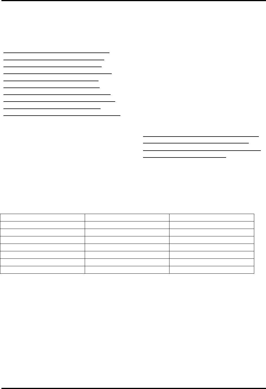
5.7 (A13) Bandpass Filter
The input to the bandpass filter is the
output of the hybrid combiner, which is
the combined output of the UHF amplifier
trays. The filter is made of aluminum
waveguide and has five resonant cavities.
The filter has five bolts for tuning
adjustments, three located in the middle
on the left and two on the right, and four
or six rods on the front of the bandpass
filter, depending upon the channel, for
coupling adjustments between the
sections. The bandpass filter also utilizes
two integral traps at -4.5 MHz and +9
MHz from FV at the top and bottom,
respectively, of the left-hand side of the
bandpass filter, looking from the rear of
the cabinet. Figure 5-2 shows the
location of the bolts used for making
tuning adjustments.
To tune the filter, connect a sweep signal
to the input of the filter and adjust the
five tuning bolts for a 6-MHz bandwidth
and a flat-frequency response across the
desired band.
Note: The bandpass ripple should be
≤
≤≤
≤0.25 dB. The 6-MHz band should
also have a minimum of 20 dB return
loss across the pass band.
See Table 5-1 for typical bandpass
values.
Table 5-1. Typical Bandpass Values
FREQUENCY INSERTION LOSS (dB) RETURN LOSS (dB)
FV-4.5 ≥ 35
FV-0.5 ≥ 20
FV≤ 0.6 ≥ 20
Fa≤ 0.6 ≥ 20
FV+8.08 ≥ 15
FV-9 ≥ 30
2FV≥ 30
10-kW UHF Transmitter with Chapter 5, Detailed Alignment Procedures
Feedforward Drive
840A, Rev. 0 5-18
Figure 5-2. Bandpass Filter
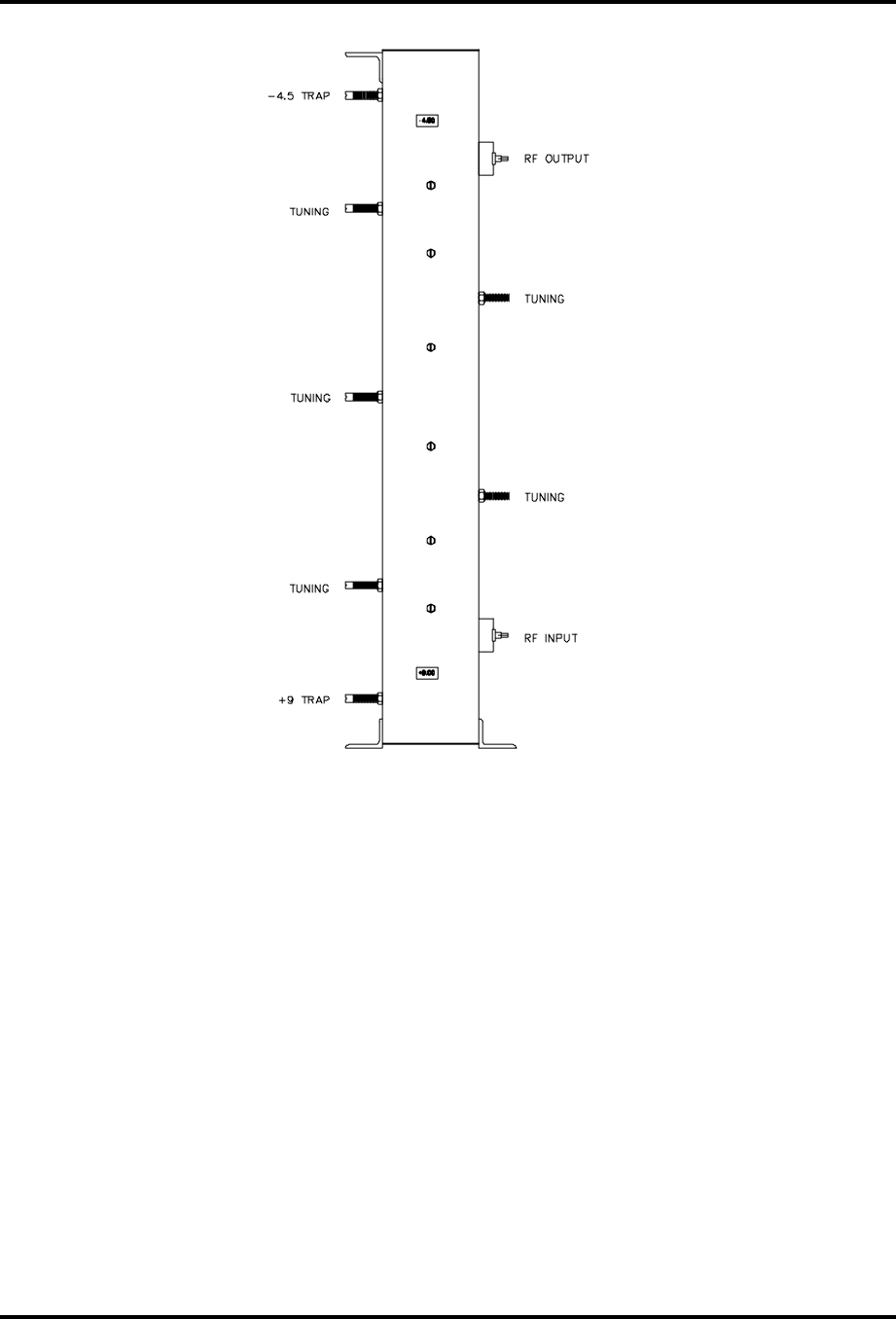
5.8 (Optional) (A14) One- or Two-
Section Trap Filter
The trap sections in the one- or two-
section trap filter have been factory
tuned and should not need major
adjustments. The trap filter is optional
and may not be part of this system.
The input to the one- or two-section trap
filter is the output of the coupler
assembly. The trap filter is comprised of
3-1/8" EIA standard transmission line
sections connected to the main
transmission line. The transmission line
assembly consists of 7/8" EIA standard
rigid coaxial components.
The traps on the output trap filter are
labeled with their center frequency
relative to the frequency of the carrier
(for example, the traps labeled -4.5 MHz
are tuned for a center frequency of 4.5
MHz lower than the frequency of the
visual carrier).
The trap sections are reflective notches
and can be adjusted across the entire
UHF frequency band. The electrical length
of the outer sleeve and the center rod of
the notch can be adjusted to tune the
notch frequency. The depth of the notch
is set by the gap between the center
conductor of the trap section and the
center conductor of the main line. Tight
coupling makes a deep notch, while loose
10-kW UHF Transmitter with Chapter 5, Detailed Alignment Procedures
Feedforward Drive
840A, Rev. 0 5-19
coupling makes a shallow notch. A one- section trap filter is shown in Figure 5-3.
Figure 5-3. One-Section Trap Filter
5.8.1 Fine Tuning
Fine tuning of the center frequency of the
notches can be accomplished with the
tuning bolts on the side of the filter
section. Loosen the nut that locks the
bolt in place and adjust the bolt to
change the frequency of the notch.
Monitor the output of the transmitter
with a spectrum analyzer and null the
distortion product with the bolt. Red field
is a good video test signal to use in order
to see the +8.08-MHz product. Tighten
the nut when the tuning is completed.
Hold the bolt in place with a screwdriver
as the nut is tightened to prevent the
bolt from slipping.
5.8.2 Major Tuning
For major tuning, such as changing the
notch depth or moving the notch
frequency more than 1 MHz, the outer
conductor and the center conductor of
the trap section must both be moved. An
RF sweep generator is required to
perform major tuning. Apply the sweep
signal to the input of the trap filter and
monitor the output. Loosen the clamp
holding the outer conductor in place and
lengthen the conductor to lower the
frequency of the notch or shorten it to
raise the frequency of the notch. Loosen
the center conductor with an Allen
wrench and move it deeper for a lower-
frequency notch or out for a higher-
frequency notch. These adjustments
must both be made to change the notch
frequency. Moving only the center
conductor or the outer conductor will
effect the notch depth and the center
frequency. The variable that is being
adjusted with this procedure is the length
of the center conductor inside the trap
filter. The gap between the trap and the
main line should not be changed. Moving
only the inner or the outer conductors
will effect the gap and the notch depth.
To only affect the notch depth, both
sections have to be moved. The notch
depth is controlled by the gap between
the center conductor and the trap
section. This gap also has an effect on
the center frequency. To deepen the
notch, shorten the outer conductor and
pull out the center conductor until the
notch is back in the same place. Move
the sections in the opposite direction to
make a shallow notch.

10-kW UHF Transmitter with Chapter 5, Detailed Alignment Procedures
Feedforward Drive
840A, Rev. 0 5-20
Note: The trap filter is typically
adjusted for a notch depth of 10 dB. The results of tuning the output trap filter
are described in Table 5-2.
Table 5-2. Results of Tuning the Output Trap Filter
TUNING ADJUSTMENT RESULT
Lengthening outer conductor only Notch frequency up, shallower notch
Shortening outer conductor only Notch frequency down, deeper notch
Inserting inner conductor deeper Notch frequency down, deeper notch
Inserting less inner conductor Notch frequency up, shallower notch
Tuning bolt in Notch frequency down
Tuning bolt out Notch frequency up
Moving both inner and outer conductors
to keep the same gap inside Center frequency moves, notch stays the
same
After the tuning has been completed,
tighten the clamp and the Allen screws
that hold the conductors. Use the fine-
tuning bolts to bring in the frequency.
The final tuning adjustments should be
completed with the transmitter driving
the output trap filter for at least one hour
to allow for warm-up drift.
5.9 Phase and Gain Adjustment of
the UHF Amplifier Trays
The following procedure was completed
at the factory and should only be
performed if one of the 250-watt
amplifier trays is replaced.
To begin this procedure, terminate the
driver cabinet into a dummy load rated
for at least 500 watts.
Preset (A8) the line stretcher rod in the
rear of the driver cabinet to mid-range.
Switch on the driver enable and adjust
the gain pot on the 3-watt tray for 25%
Driver Output Power. Adjust the phase
control upward. If the % Driver Output
Power goes up, continue to adjust the
line stretcher until either the peak is
reached or the end-of -travel is reached.
If the % Output Power goes down, push
(A8) the line stretcher downward.
If the end-of-travel is reached on the
phase adjust as it is being moved
upward, reset the phase control to mid-
range and add a 2-inch length of cable to
the input of (A6) the 250-watt amplifier
tray at J1. Readjust (A8) the line
stretcher rod until a peak is reached or
until end-of-travel is achieved. If end-of-
travel is reached, repeat the above
procedure, but replace the 2-inch length
cable with a 4-inch length of cable.
If the amount of downward range runs
out, add a 2-inch phase cable to the
input of (A7) the 250-watt tray and start
mid-range with (A8) the line stretcher. If
a visual power peak is reached, lockdown
(A8) the line stretcher knob. If a peak is
not reached, replace the 2-inch cable
with a 4-inch cable and repeat this
procedure.
5.10 Calibration of the Forward
Output Power Level of the Amplifier
Cabinet
Note: Perform the following
procedure only if the power
calibration is suspect. The amplifier
cabinet output must be terminated
into a minimum dummy load of 10
kW.
Switch the transmitter to Standby and
perform the following adjustments, with
no aural present, by removing jumper
cable W1, aural IF loop-through,
connected to J16 on the sync tip clamp
on the sync tip clamp/modulator board

10-kW UHF Transmitter with Chapter 5, Detailed Alignment Procedures
Feedforward Drive
840A, Rev. 0 5-21
(1265-1302). Connect a sync and black
test signal to the video input jack of the
UHF exciter tray. Switch the transmitter
to Operate.
Next, set up the transmitter for the
appropriate average output power level
(sync + black 0 IRE setup/wattmeter
=5950 watts; sync + black 7.5 IRE
setup/wattmeter=5400 watts).
Note: The transmitter must have 40
IRE units of sync.
Adjust R28, visual and audio calibration,
on (A19-A2) the visual/aural metering
board (1161-1103) for 2 volts on FL5 on
the visual/aural metering assembly.
Adjust R29 on the same board for 100%
on the front panel meter in the % Visual
Output position.
With the spectrum analyzer set to zero
span mode, obtain a peak reference on
the screen with the following readings:
• Resolution bandwidth – maximum
• Span – 0 MHz
• Scale – linear
Reconnect jumper cable W1 to J16 on
(A5) the sync tip clamp on the modulator
board. Turn the power adjust pot on the
3-watt amplifier tray front panel until the
original peak reference level is attained.
Peak C5 for a maximum aural power
reading and then also adjust R11 for a
100% aural power reading. Switch to the
Visual Output Power position and adjust
R39 for 100% Visual Power. Turn the 3-
watt amplifier tray front panel gain pot
fully CCW and switch the exciter to
standby. Re-terminate the drive output
into the diacrode cavity.
5.11 Calibration of Reflected
Metering
Adjust the 3-watt amplifier tray front
panel gain pot for 15% Visual Power on
the metering control panel. Switch S4,
the power meter, to the Reflected
position. Reverse the J6 cable and the J4
termination on (A18) the final output
coupler. Adjust R6 on (A19-A1) the single
peak detector board (1164-1403) in the
visual/audio metering assembly for a
15% Reflected Power reading. Return J4
and J6 to their original positions.
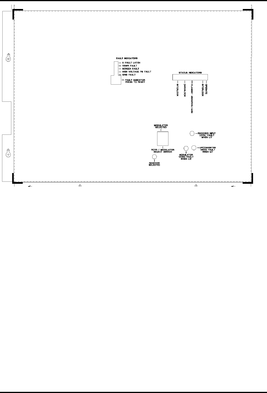
5.12 Board Level Adjustments
5.12.1 (A1) Control Logic Board
(1137-1402; Appendix B)
The rear of the metering control panel is
shown in Figure 5-4. The control logic
board is in the metering control panel
and provides the circuitry needed for the
control of the automatic on/off sequence
of the transmitter and the monitoring of
the operation of the transmitter for fault
conditions. An Operate command and the
interlocks for the transmitter are also
connected to the board.
The control logic board monitors the air-
on sense, the filament-on sense, the
bias-on sense, the high voltage-on sense,
and the screen-on sense commands
during each step of the automatic turn-
on procedure. The board also provides
the on-command outputs in the proper
sequence and enables to the Command
Status and Operating Status LEDs on the
front panel. The fault circuits monitor the
operation of the power supplies and the
tube, the air flow to the tube, and the
temperature of the transmitter; the
board will shut down the transmitter if
any of these faults occur.
The board supplies the air-on, filament-
on, bias-on, screen-on, high voltage-on,
and RF-on commands to the transmitter.
In addition, the board is connected to the
High-Voltage Enable/Disable switch to
provide commands to magnetic latching
relay K1.
10-kW UHF Transmitter with Chapter 5, Detailed Alignment Procedures
Feedforward Drive
840A, Rev. 0 5-22
Figure 5-4. Metering Control Panel (Rear)
The status indicators on the board, and a
description of what each of the indicators represent when they are lit, are listed in
Table 5-3.

10-kW UHF Transmitter with Chapter 5, Detailed Alignment Procedures
Feedforward Drive
840A, Rev. 0 5-23
Table 5-3. Control Logic Board Status Indicators
LED FUNCTION DESCRIPTION
DS1 OPERATE Indicates that transmitter is
in the Operate mode
DS2* INTLK. (INTERLOCK)
Whole system shutdown
interlock used for external
connections; normally
jumpered across on the
remote control and interface
assembly
DS3 AIR
Indicates that air pressure
switch is closed and there is
sufficient air flow around the
tube
DS4 FIL (FILAMENT) Indicates that filament
power supply is operating
DS5 FIL UV (FILAMENT UNDER
VOLTAGE)
Indicates that filament
voltage is above the preset
of the lower threshold point
DS6 BIAS Indicates that bias power
supply is operating
DS7* INTLK (INTERLOCK)
High-voltage shutdown
interlock; normally
jumpered across on the
remote control and interface
assembly
DS8 H.V. (HIGH VOLTAGE) Indicates that high-voltage
supply is on and above the
preset level
DS9* INTLK (INTERLOCK)
Interlock is not used in the
10-kW amplifier; jumpered
across on the control logic
board (J3, pins 9 and 10)
DS10 RF (DRIVE)
Indicates that Mute
command has been
removed from the
upconverter tray
Note: If the exciter and
the aural and visual
driver sections are
operating normally, the
transmitter will have an
output.
DS11 FAULT 3
Indicates that three faults
have occurred in succession
or within a given time frame
Note: This action will
remove the high voltage,
screen, and RF drive.

10-kW UHF Transmitter with Chapter 5, Detailed Alignment Procedures
Feedforward Drive
840A, Rev. 0 5-24
LED FUNCTION DESCRIPTION
DS13 VSWR
Indicates that a voltage
standing wave ration that
exceeds 12.5% of reflected
power
DS14 SCREEN Indicates that the screen
current is greater than ±120
mA
DS15 HVPS
Indicates that the cathode
current exceeds 5 amps or
the high-voltage power
supply current exceeds the
preset limit
DS12 GRID Indicates that the bias
current exceeds the preset
limit of ±50 mA
S1 IND. RESET
When pushed, will only reset
the fault indicator LEDs
(DS12 through DS13); will
not reset the transmitter or
the DS11 LED if lit. To reset
the DS11 LED, the fault
reset switch on the front
panel of the metering
control panel must be used.
* The three Interlock indicators should be lit at all times unless they are connected to an
external sensor and a fault occurs.
5.12.2 Filament Power Supply Board
(1293-1304; Appendix B)
The following steps will allow a thorough
test of the software programmed into the
microcontroller and used on the filament
power supply board (1293-1304):
1. Install a pre-programmed U4, using
the latest 1293-6316 software
version, into its socket on the
filament power supply board (1293-
1304).
2. On the filament power assembly
(1299-1107), connect +12 volts to
TB1-2, -12 volts to TB1-1, and
ground to TB1-3.
3. Disconnect J3 from the filament
power supply board (1293-1304) and
turn on the external DC voltages.
Verify that DS1 is blinking at a 1-Hz
rate.
4. Turn off the external DC voltages.
Reconnect J3 to the controller board;
220 VAC to TB2-1 and TB2- 2; and
ground to TB2-3. Connect the power
supply output to a .1-ohm, 300-watt
resistor, TB2-5 to the (+) side of the
resistor, and TB2-6 to the (–) side.
Turn on the resistor-cooling fan.
5. Turn on the external voltages;
momentarily close SW1-8 and then
reopen it. Verify that J3-1 is 0.0 volts
and DS1 is blinking at a 1-Hz rate.
The power supply output should be
1.5 volt at this point and TB1-8
should have a low voltage. Take note
of the time; a 10-minute timeout
must be measured from power
application to the board.
6. At this point, DS1 should be blinking
at a 1-Hz rate. Measure the voltage
on TB1-7; it should be +12 volts.
Measure the output voltage of the

10-kW UHF Transmitter with Chapter 5, Detailed Alignment Procedures
Feedforward Drive
840A, Rev. 0 5-25
filament power supply; it should be
1.5 volts.
7. Verify that J3-1 remains at 0 volts
and DS1 blinks at a 1-Hz rate while
the following actions are performed:
• Switch on SW1-3 and turn on
SW1-5, SW1-6, and SW1-7
individually (no time limit).
• Connect +12 volts to TB1-5 for
less than 5 seconds.
• Turn off the external +/-12-volt
power supply for less than 5
seconds.
• Remove J6 from the controller
board for less than 5 seconds.
• Ground TB1-6 several times and
then leave it unconnected.
• Turn off the 220 VAC at TB2-1
and TB2-2 for less than 5
seconds.
8. After 10 minutes, DS1 should begin
blinking at a 2-Hz rate. This signals
that the 10-minute time-out period
has successfully been completed. At
this point, with SW1-3 on, switch
SW1-5 on. J3-1 should be 0 volts.
Switch SW1-5 off and SW1-6 on; J3-
1 should be 4.625 volts. Switch SW1-
6 off and SW1-7 on; J3-1 should be
5.0 volts. If necessary, adjust R6 on
the controller board until a reading of
5.0 volts is obtained.
9. Ground TB1-6 to simulate a filament-
on command and note the time. The
voltage at TB1-7 should be 0 volts;
220 VAC should now be present at
TB2-7 and TB2-8; and DS1 should be
blinking at a 4-Hz rate. The voltage at
J3-1 should increase to 4.625 volts
over a three-minute time frame.
During this ramp-up phase, the
following conditions should not cause
DS1 to stop blinking at its 4-Hz rate
or the ramp-up to discontinue:
• Connecting TB1-5 to +12 volts for
less than 5 seconds
• Turning off the external +/-12-
volt power supply for less than 5
seconds
• Removing J6 from the controller
board for less than 5 seconds
• Turning off the 220 VAC at TB2-1
and TB2-2 for less than 5 seconds
• Switching SW1-5, SW1-6, and
SW1-7 on and off individually (no
time limit)
Note: Leaving any of the above
conditions on for longer than 5
seconds should cause the filament
power supply to revert back to the
10-minute warm up cycle (J3-1 at 0
volts).
10. Remove the ground from TB1-6. The
voltage at J3-1 should begin to
decrease. Re-ground TB1-6. This
should cause J3-1 to start ramping
back up. Once J3-1 is at 4.625 volts
(5.2 volts across the load resistor),
DS1 should not be blinking. Perform
all of the tasks in step 10 and verify
that J3-1 remains at 4.625 volts. It
should be noted once again that
performing these tasks for longer
than 5 seconds should cause the
voltage at J3-1 to again return to 0
volts for 10 minutes.
11. Remove the ground from TB1-6. The
5 volts at J3-1 should start to ramp
down. Re-ground TB1-6. The voltage
at J3-1 should start to ramp back up.
Remove the ground again. J3-1
should return to 0 volts over a 3-
minute time frame; TB1-7 should
remain at 0 volts; TB2-7 and TB2-8
should not have 220 VAC present;
and DS1 should be blinking at a 4-Hz
rate. Perform the same tasks as in
step 10 and verify that they have no
effect on the ramp-down cycle.
Taking any more than 5 seconds for

10-kW UHF Transmitter with Chapter 5, Detailed Alignment Procedures
Feedforward Drive
840A, Rev. 0 5-26
any of them should cause J3-1 to
return to 0 volts for the 10-minute
warm-up cycle.
12. Remove all of the connections to the
filament power supply assembly. The
test is complete.
5.12.3 10-kW Bias Power Supply
Board, 230 VAC (1181-1001;
Appendix B)
With the high voltage disabled,
disconnect the bias cable from the
TH18610 cavity assembly. Measure the
DC voltage on the cable output. Adjust
R14 on the bias supply board to calibrate
the bias voltage on the meter on the
metering control panel on the amplifier
assembly.
To calibrate the bias current, attach a
variable power supply and current
metering device with the (+) lead
connected to the R5/R4 junction and the
(-) lead to ground. Adjust the current to
10 mA and adjust R6 for a 10-mA
reading on the current meter on the
metering control panel.
5.12.4 Screen Power Supply Board
(1293-1319; Appendix B)
With the high voltage enabled, and the
screen power supply breaker turned off,
disconnect the screen supply cable from
the TH18610 cavity. Turn on the screen
power supply breaker and measure the
voltage with a meter capable of at least
600 VDC. Adjust R14 on the screen
power supply board (1293-1319) for 500
volts. Adjust R20 on the same board for
500 volts of screen power supply voltage
on the metering control panel.
To calibrate the screen current, turn off
the screen power supply breaker. Attach
a variable power supply and current
measuring device with the (-) lead
connected to the R7/R8 junction and the
(+) lead connected to ground. Adjust the
power supply current until a reading of
10 mA is obtained on the current
measuring device. Adjust R9 on the
screen power supply board for a 10-mA
reading on the current meter on the
metering control panel. The screen
current is now calibrated.
5.12.5 Dual Polarity Fault Sensing
Board (1016-1402; Appendix B)
To align the screen current fault, switch
off the screen breaker and disable the
high voltage. Attach a variable power
supply and a current meter as described
in the alignment procedures for the
screen power supply board (1293-1319)
in Section 5.12.4. Adjust the current for
90 mA and turn R6 until the Screen Fault
LED DS14 lights. Reduce the current and
DS14 should go out after fault reset S9
on (A1) the control logic board (1137-
1402) has been pushed.
To align the screen overcurrent fault
(reverse polarity), reverse the variable
power supply connections and repeat the
alignment procedures for the screen
current fault while using R12 to adjust
the trip point.
To align the bias overcurrent fault, switch
off the bias supply breaker; the
transmitter will be in the Standby mode.
Attach a variable power supply and a
current meter as described in the
alignment procedures for the 10-kW bias
power supply board, 230 VAC (1181-
1001), in Section 5.12.3. Adjust the
power supply for a 30-mA current and
adjust R25 until the Bias Current Fault
LED DS12 lights. Slightly reduce the
current and push fault reset switch S9 on
(A1) the control logic board (1137-1402).
To align the bias overcurrent fault
(opposite polarity), reverse the variable
power supply connections and repeat the
procedure described above while using
R18 to adjust the trip point.

10-kW UHF Transmitter with Chapter 5, Detailed Alignment Procedures
Feedforward Drive
840A, Rev. 0 5-27
5.12.6 Inverting Fault Sensing Board
(1016-1401; Appendix B)
To align the plate overcurrent function,
attach a variable power supply and a
current meter as described in the
alignment procedure for (A9) the current
metering board (1084-1205) in Section
5.12.9. Adjust the current for 5 amps
and turn R6 until the Plate Current Fault
LED DS15 on (A1) the logic control board
(1137-1402) lights. Slightly reduce the
current and push fault reset switch S9 on
(A1) the control logic board (1137-1402).
DS15 should go out.
To align the reflected power fault, set the
transmitter for 12.5% output power.
Reverse the cable at J6 and the
attenuator on J5 of (A2-A2) the diacrode
output coupler. Adjust R12 until the
VSWR Fault LED DS7 illuminates.
Note: This is a 3-fault adjustment.
The transmitter logic looks for the
same fault three times before
latching in a permanent fault state.
Reverse the J5 and J6 connections and
clear the fault by pushing the 3-fault
reset switch on the metering control front
panel.
To align the bias-on sense, the high
voltage should be enabled and there
should be no RF drive. Adjust the bias
voltage for 2 amps static plate current.
Adjust R18 until the Bias Status LED
DS18 goes out on the metering control
panel. Return the bias voltage to the
original reading of 1.5 amps of static
phase current.
5.12.7 Fault Sensing Board (1293-
1307; Appendix B)
To align the screen sense, place the
exciter tray in the Standby mode. Adjust
R14 on the screen power supply board
fully CCW (approximately 430 volts).
Adjust R6 until the Screen Status LED
DS20 just goes out. Return R14 to 500
volts screen voltage.
To align the high-voltage sense, turn off
CB1 and discharge all high voltage.
Caution: Make sure that the high-
voltage power supply cabinet is
safely turned off.
Remove fuse F1 from one of the high-
voltage rectifier boards (A5, A6, or A7).
Turn the screen breaker off and bring the
transmitter power up normally (with the
high voltage enabled). Adjust R12 until
the High-Voltage Status LED DS19 on the
metering control panel goes out. Shut
down the transmitter and rectifier F1 on
the rectifier board while making sure that
the high-voltage power supply cabinet is
safely discharged.
To align the filament ready function, set
the filament voltage to 5.2 volts. Adjust
R18 until the Filament Status LED DS17
just goes out and then turn the pot until
DS17 just comes back on.
To align the filament undervoltage, set
the filament voltage to 5.2 volts. Place
the transmitter in the Standby mode by
using S5 on the metering control panel.
At ≈5.0 volts, adjust R25 until the
Filament Undervoltage LED DS5 on (A1)
the control logic board (1137-1402) just
goes out. Return the transmitter to
Operate. DS5 should be lit when the
filament voltage is normal (5.2 volts).
5.12.8 Transmitter Control Board
(1137-1003; Appendix B)
To align the VSWR fault adjust on the
transmitter control board, turn the
transmitter power down to 10%. Using
the 3-watt amplifier tray front panel gain
pot, reverse the cable on J6 and the
attenuator on J5 on (A2-A2) the output
coupler. Adjust R44 until the VSWR
Cutback LED DS23 just begins to light on
the front panel of the metering control
panel. Place J5 and J6 in their original
positions.
To align the output fault adjust, turn the
transmitter output power down to 10%.

10-kW UHF Transmitter with Chapter 5, Detailed Alignment Procedures
Feedforward Drive
840A, Rev. 0 5-28
Adjust R38 until the RF Request LED
DS21, on the metering control front
panel in the Operating Status section,
just goes out. When the transmitter
output power is above 10%, the LED
should be illuminated.
5.12.9 (A9) Current Metering Board
(1084-1205; Appendix B)
Caution: Extreme care must be taken
when aligning the current metering
board.
First, disable the high-voltage section of
the high-voltage power supply by turning
circuit breaker CB2 (HV) to the Off
position. Connect a variable power supply
capable of 5 amps and a current
measuring device across E1 (-) and E2
(+) on (A9) the current metering board
(1084-1205). Set the current for 4 amps
on the measuring device. Adjust R3 on
the board for a 4-amp reading on the
current meter on the metering control
board.
This completes the detailed alignment
procedures for the transmitter. If a
problem occurred during the alignment,
refer to the detailed alignment procedure
for that tray.