UBS Axcera LU500AL 500-Watt UHF Translator User Manual 382629
UBS-Axcera 500-Watt UHF Translator 382629
Contents
- 1. Section 5 Users Manual Page
- 2. Title Page External Amplifier
- 3. Table of Contents External Amplifier
- 4. Chapter 1 External Amplifier
- 5. Chapter 2 External Amplifier
- 6. Chapter 3 External Amplifier
- 7. Chapter 4 External Amplifier
- 8. Chapter 5 External Amplifier
- 9. Appendix Pages External Amplifier
- 10. Drawings List External Amplifier
- 11. Title Page Exciter
- 12. Table of Contents Exciter
- 13. Chapter 1 Exciter
- 14. Chapter 2 Exciter
- 15. Chapter 3 Exciter
- 16. Chapter 4 Exciter
- 17. Chapter 5 Exciter
- 18. Appendix Pages Exciter
- 19. Drawings List Exciter
- 20. Data Sheet Exciter and Amplifier
Chapter 4 External Amplifier

LX Series Power Amplifier Assembly Chapter 4, Circuit Descriptions
LX Series, Rev. 0 4-1
Chapter 4
Circuit Descriptions
The RF from the exciter/driver assembly
connects from the RF Output “N” Jack J25,
through a RG-55 cable, to the PA RF Input
SMA Jack J200, located on the rear of the
PA chassis assembly. The RF Input is
cabled through UT-141 to port J111 on
the main chassis. Jack J1 on the PA
module assembly connects to the J111
port when the module assembly is slid
into place.
The RF output from the 2 way UHF
combiner connects to the PA RF Output
Jack J2, located on the rear of the PA
Module. Jack J2 on the PA module
connects to the J115 port, on the main
chassis assembly, when the module
assembly is slid into place.
4.1 (A4) Power Amplifier Module
Assembly (1302868; Appendix B)
The Power Amplifier Module Assembly
contains (A1) a UHF Phase/Gain Board
(1303213), (A2) a 150W Driver Pallet,
Dual Output (1303293), (A3 & A4) UHF
RF Module Pallet Assemblies (1300116),
(A5) a 2 Way UHF Combiner Assembly
(1303208), (A6) an Amplifier Control
Board (1301962) and (A7) a
Temperature Sensor IC.
4.1.1 (A1) UHF Phase/Gain Board
(1303213; Appendix B)
The RF input from J1 on the PA assembly
connects to J1 on the Phase/Gain Board.
The UHF phase/gain board provides the
circuits that adjust the gain and the
phase of the RF signal for the PA
amplifier assembly in which it is
mounted. The input signal connects to
the gain circuit through the capacitor
C13. The gain circuit consists of U1,
R16, CR4, R22, R17, CR5, R23, R27 and
the gain pot, R25. U1 is a 90°, 2-way
splitter. The signal at pin 1 of U1 is split
and applied to pins 3 and 4. The signal
reflects off CR4 and CR5 and is passed to
pin 2. The gain between pins 1 and 2
changes with the voltage applied across
CR4 and CR5. This voltage is controlled by
the gain-adjust pot R25. The more
positive the voltage, the more the diodes
CR4 and CR5 conduct therefore the less
gain through the circuit. The gain
controlled output is coupled through C14
and the pi-type divider circuit consisting of
R8, R5 and R9 that drops the level before it
applied to the phase-shifter circuit.
The level controlled signal connects to the
phase-shifter circuit that consists of U2,
C20, C21, CR2, and CR3. U2 is a 90°, 2-
way splitter. The signal at pin 1 of U2 is
split and applied to pins 3 and 4. The signal
reflects off CR2 and CR3 and is passed to
pin 2. The phase shift between pins 1 and
2 changes with the voltage applied across
CR2 and CR3. This voltage is controlled by
the phase-adjust pot R24 through R26,
R18 and R19. +12 VDC from an external
switching power supply is applied to J3 on
the board and is used as the reference that
is applied to the phase-control pot. The
gain and phase controlled output connects
to J2 on the board.
4.1.2 (A2) 150 Watt Driver Pallet
Assembly, Dual Output (1303293;
Appendix B)
The output of the Phase/Gain Board is
connected to the input J1 of (A2) the 150
Watt UHF amplifier assembly. The
assembly contains a 150 Watt CW UHF
Driver Board, Dual Output (1303169).
4.1.3 150 Watt Driver, Dual Output
(1303169; Appendix B)
The board operates class AB and is a
highly linear broadband amplifier for the
frequency range of 470 to 860 MHz. It can
deliver an output power of 150 watts
(CW) with approximately 14 dB of gain.
LX Series Power Amplifier Assembly Chapter 4, Circuit Descriptions
LX Series, Rev. 0 4-2
The amplification circuit consists of
LDMOS transistors Q1 and Q2 connected
in parallel and operating class AB. The
paralleling network is achieved with the
aid of 3 dB couplers U3 and U4. The
quiescent current settings are achieved
by means of potentiometers R6 and
R10. C39 and C38 are adjusted for best
response. The settings are factory
implemented and should not be altered.
PIN diode VR1 is a variable-damping
circuit that is used to adjust the
amplification of the module. The
adjustment is performed with the Gain
potentiometers R10 and R6. A
readjustment of the amplification may
be required, after repair work, to ensure
that the PAs in multiple PA translators
deliver the same output power.
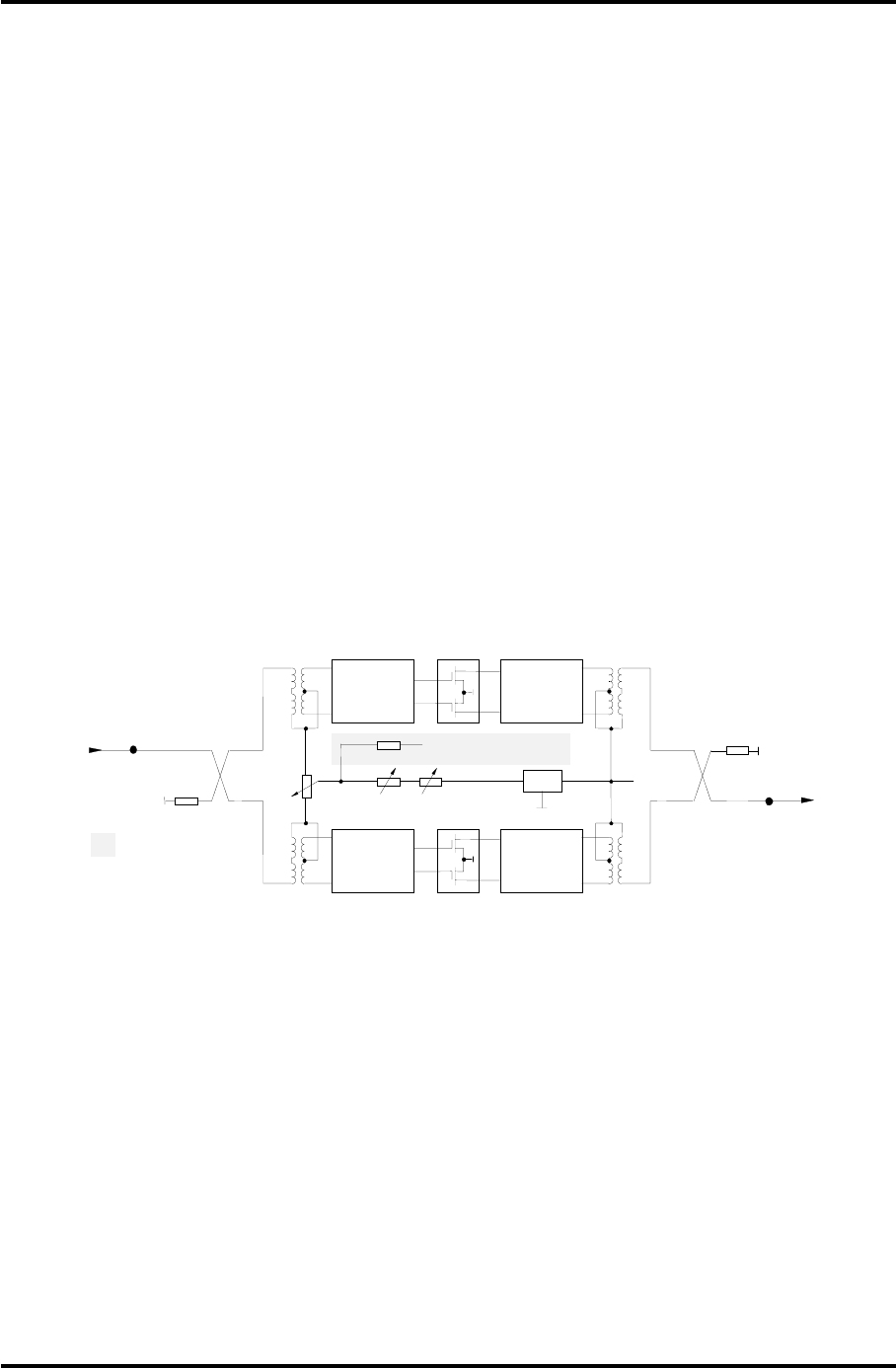
4.1.4 (A3 & A4) UHF Module
Assembly, RF Module Pallet, Philips
(1300116;Appendix B)
The UHF Module Assembly, 250-watt
module (Figure 4-1) is a broadband
amplifier for the frequency range 470 to
860 MHz. The amplifier is capable of
delivering an output power of 70 Wrms.
The amplification is approximately 13 dB.
The amplification circuit consists of the
parallel connected push-pull amplifier
blocks V1 and V2 operating in class AB. In
order to match the transistor impedance
to the characteristic impedance of the
input and output sides, matching networks
are placed ahead and behind the amplifier
blocks. Transformers Z3 to Z6 serve to
balance the input and output signals. The
paralleling circuit is achieved with the aid
of 3-dB couplers Z1 and Z2.
The working point setting is factory
implemented by means of potentiometers
R9, R11, and R12 and should not be
altered.
V 1
3 dB Coupler
Z 2
RF
Output
RF
Input
3 dB Coupler
Z 1
R 2
R 1
Matching
Network
Matching
Network
V 2
Matching
Network
Matching
Network
Z 3 Z 5
Z 4 Z 6
+Uop
N 1
R 11 R 12
R 9
R 10
Dynamic
Figure 4-1. UHF Amplifier Module, 250 Watts
4.1.5 (A5) 2 Way UHF Combiner
Assembly (1303208; Appendix B)
The 2 Way UHF combiner board assembly
combines the two outputs of the UHF
Module Assemblies and also provides
forward and reflected power samples of
the output to (A6) the amplifier control
board where it connects to the input of
the overdrive-protection circuit.
The RF inputs to the 2 way UHF combiner
assembly, from the UHF amplifier
modules, are soldered to the external
connection points J3 and J4. The RF is
combined by the stripline tracks and R5 a
100 ohm matching resistor across the two
inputs, to the RF Output solder connection
point at J5. A hybrid-coupler circuit picks
off a power sample that is connected to
SMA type connector jack J1 as the forward
power sample. Another power sample is
taken from the coupler circuit that is
connected to SMA type connector jack J2
as the reflected power sample. Two 50Ω
terminations, created from two 100 ohm
resistors in parallel, used as dissipation
loads, connect from the forward and
reflected ports to ground.

LX Series Power Amplifier Assembly Chapter 4, Circuit Descriptions
LX Series, Rev. 0 4-3
4.1.6 (A5) Amplifier Control Board
(1301962; Appendix B)
The amplifier control board provides LED
fault and enable indications on the front
panel of the module and also performs
the following functions: overdrive
cutback, when the drive level reaches the
amount needed to attain 110% output
power; and overtemperature, VSWR, and
overdrive faults. The board also provides
connections to the LCD Display for
monitoring the % Reflected Power, %
Output Power, and the power supply
voltage.
Page 1
U4, located upper center of page, is an in
circuit microcontroller. The controller is
operated at the frequency of 3.6864 MHz
using crystal Y1. Programming of this
device is performed through the serial
programming port J2. U4 selects the
desired analog channel of U1 through the
settings of PA0-PA3. The outputs of Port
A must be set and not changed during an
analog input read of channels PA5-PA7.
PA4 of U4 is a processor operating LED
that monitors the +/-12 VDC. PA5 is
used to monitor the +12VDC supply to
the board. PA6 is the selected channel of
analog switch U1. PA7 is connected to a
via, V10, for future access.
U6 is a serial to RS-485 driver IC. U7 is
a watchdog IC used to hold the
microprocessor in reset, if the supply
voltage is less than 4.21 VDC. U7
momentarily resets the microcontroller if
Pin 6 (!ST) is not clocked every second.
A manual reset switch is provided but
should not be needed.
Upper left corner U3 is used to determine
where the amplifier control board is
located. The eight inputs come from the
main amp connector and are used to set
the SCADA address of the controller.
Pull-up resistors set a default condition of
logic high.
U5 below U3 is used for getting digital
input information of the board. Page two
has several monitoring circuits that provide
information on the amplifier’s status. Many
of these circuits automatically shut down
the amplifier if a specific fault occurs.
U8 below U5 is used to control four board
mounted status LEDs. A FET is turned On
to shunt current away from the LED to turn
it Off. U9 below U8 is used to enable
different features within the software.
Actual use is to be determined.
Page 2
In the lower right corner are voltage
regulator circuits. U22 should allow for
0.14 amps of power using its 92 C/W
rating if Ta = 60°C max and Tj = 125°C
max 0.26 amps can be obtained from U22
if the mounting pad is 0.5 square inches.
The controller will not need this much
current.
U23 and U24 are low drop out +5 VDC,
voltage regulators with a tolerance greater
than or equal to 1%. 100mA of current is
available from each device but again the
controller will not need this much current.
In the upper left section are circuits with
U12 and U13. U12 is used to generate a
regulated voltage that is about 5 volts less
than the +32 VDC supply, approximately
+26.25 VDC. When the +32 VDC supply is
enabled, the circuitry around U13B is used
to provide gate voltage to Q10 that is 5
volts greater than the source pin of this
FET. The gate of Q10 can be turned Off by
any one of a few different circuits.
U10A is used to turn Off the gate of Q10 in
the event of high current in amplifier #1.
At 0.886 VDC the current to amplifier #1
should be greater than 5 Amps. U11B is
used to turn off the Q10 FET, if high
current is detected in amplifier #2. U11A
is used to turn off the Q10 FET, if high
current is detected in amplifier #3. With
2.257 VDC at Pin 5 of U11B or Pin 3 of
U11A, the voltage output of current sense

LX Series Power Amplifier Assembly Chapter 4, Circuit Descriptions
LX Series, Rev. 0 4-4
amplifier U17 or U18 at high current shut
down should be greater than 15 Amps.
U14B is used to turn Off the gate of Q10
in the event of high power supply
voltage, approximately +35.4 VDC.
U14A is used to keep the FET disabled in
the event of low power supply voltage,
approximately +25.4 VDC.
Current monitoring sections of the board.
The ICs U16, U17 and U18 along with
associated components set up the
current monitoring sections of the board.
R67, R68 and R69 are 0.01Ω/5W 1%
through hole resistor is used for
monitoring the current through several
sections of the amplifier. The voltage
developed across these resistors are
amplified for current monitoring by U16,
U17 or U18. The LT1787HVCS8 precision
high side current sense IC amplifier
accepts a maximum voltage of 60 VDC.
The 43.2 kΩ resistor from pin 5 to
ground sets the gain of the amplifier to
about 17.28. This value is not set with
much accuracy since the manufacturer
internally matches the resistors of this
part but their actual resistance value is
not closely defined. A trimming resistor
is suggested to give a temperature
stability of –200 ppm/C, but instead the
microcontroller will determine the exact
gain of the circuit and use a correction
factor for measurements. Circuit loading
components are located in the lower
portion of each current monitoring circuit.
These components allow for short
duration high current loading of the
supply. By measuring the current
through the sense resistor with and
without the additional four 30.1 Ω 1%
resistors. For very short duration pulses,
a 1206 resistor can handle up to 60
watts. The processor requires 226 uSec
per conversion. A supply voltage of +32
VDC will pass 1.06 amps + 1% through
the load resistors.
A6 is a temperature sensor thermistor
that is used to monitor the temperature
of the module's heat sink. It connects
to J6 pins 1 & 2 on the board wand is
wired to the comparator IC U10B. If the
temperature increases above 75°C the
output will go Low that is used as a
temperature fault output, which generates
a Fault alert at U15A and disables
Amplifier #1.
Aural, Visual/Average and Reflected power
detector sections of the board.
Page 3
A Forward Power Sample enters the board
at SMA Jack J3 and is split. One part
connects to J4 on the board that is cabled
to J1, the SMA Forward Power Sample
Jack, located on the front panel of the
assembly. The other part of the split
forward power sample is detected by CR17
and the DC level amplified by U25A. The
output of U25A at pin 1 is split with one
part connected to the Aural Power sample,
which is not used in this digital translator.
The other split output connects to U265A
that is part of the Forward Average Power
circuit. The detected level is connected to
L4 that is part of an intercarrier notch filter
circuit that is tuned to eliminate the 4.5
MHz aural intercarrier, if present. The
Average power sample is amplified by
U26D and connected through the average
calibration pot R166 to U26C. The output
of U26C is connected to the comparator IC
U26B that has Aural Null and Offset Null, if
present in the system, connected to the
other input. The output Average Forward
power level connects to J9 pin 2 of the
board.
A Reflected Power Sample enters the board
at SMA Jack J5 and is detected by CR20
and the DC level amplified by U28B. The
output of U28B at pin 7 is connected
through the reflected calibration pot R163
to U28C. The output is split with one part
connected to J9 pin 5, the Reflected Power
Output level of the board. The other part
of the split from U28C connects to the
comparator IC U28D that has a reference
level connected to the other input. If the
reflected level increases above the
reference level a low output is produced

LX Series Power Amplifier Assembly Chapter 4, Circuit Descriptions
LX Series, Rev. 0 4-5
and connected to the Reflected Power
Shutdown circuit at CR28. The low shuts
off Q14 causing pin 3 to go high that is
connected to the inverter U15C. The
output of U15C goes low producing a
Reflected Power Fault that is connected
to an output of the board, the Fault Alert
circuit and also shuts down Amplifier #1.
Gain of the power measurements is
completed through software. Only the
Aural Null and Offset Null need to be
done through front panel pots.
4.2 Power Supply Assembly (1302863;
Appendix B)
The Power Supply Assembly contains (A1)
a +32V/2000W switching power supply
(1301504) and (A2) a ±12V/40W
switching power supply (1303242). The
+32VDC connects through J1 (+32VDC)
and J2 (RTN) to the rest of the amplifier
assembly. The +/-12VDC outputs, the
+32VDC control lines and the 220VAC
connect to the assembly through Jack J3.
Both power supplies contain no customer
adjustments.
This completes the description of the Power
Amplifier Module Assembly and the Power
Supply Assembly.