Baron Services XDD-1000C C-BAND DOPPLER WEATHER RADAR User Manual
Baron Services Inc C-BAND DOPPLER WEATHER RADAR
Contents
- 1. Modulator Manual
- 2. Users Manual Part 1
- 3. Users Manual Part 2
- 4. Users Manual Part 3
- 5. S10 OPERATION AND MAINTENANCE MANUAL
- 6. S10 FAST TRAC MILLENIUM USERS GUIDE
- 7. S10 TECHNICAL MANUAL
- 8. S10 RECEIVER AND PROCESSOR USERS MANUAL PART 1
- 9. S10 RECEIVER AND PROCESSOR USERS MANUAL PART 2
- 10. S10 RECEIVER AND PROCESSOR USERS MANUAL PART 3
S10 RECEIVER AND PROCESSOR USERS MANUAL PART 1

DRAFT
RVP8
Digital IF Receiver/Doppler Signal Processor
User’s Manual
May 2003
Copyright 2003 SIGMET, Inc.
The designs and descriptions contained in this manual may not be copied, translated or
reproduced in any form without the prior written consent of SIGMET, Inc.

Table of Contents
RVP8 User’s Manual
12 May 2003
i
Table of Contents
Hardware Limited Warranty x . . . . . . . . . . . . . . . . . . . . . . . . . . . . . . . . . . . .
Preface xi . . . . . . . . . . . . . . . . . . . . . . . . . . . . . . . . . . . . . . . . . . . . . . . . . . . . . . .
1. Introduction and Specifications 1–1 . . . . . . . . . . . . . . . . . . . . . . . . . . . . . . . .
1.1 System Configuration Concepts 1–4 . . . . . . . . . . . . . . . . . . . . . . . . . . . . . . . . . . . . .
1.1.1 IFD IF Digitizer 1–9 . . . . . . . . . . . . . . . . . . . . . . . . . . . . . . . . . . . . . . . . . . .
1.1.2 Digital Receiver PCI Card (RVP8/Rx) 1–10 . . . . . . . . . . . . . . . . . . . . . . . . . .
1.1.3 Mother Board or Single-Board Computer (SBC) 1–13 . . . . . . . . . . . . . . . . . .
1.1.4 Digital Transmitter PCI Card (RVP8/Tx) 1–13 . . . . . . . . . . . . . . . . . . . . . . . .
1.1.5 I/O-62 PCI Card and I/O Panel 1–15 . . . . . . . . . . . . . . . . . . . . . . . . . . . . . . . .
1.2 Comparison of Analog vs Digital Radar Receivers 1–17 . . . . . . . . . . . . . . . . . . . . . .
1.2.1 What is a Digital IF Receiver? 1–17 . . . . . . . . . . . . . . . . . . . . . . . . . . . . . . . .
1.2.2 Magnetron Receiver Example 1–18 . . . . . . . . . . . . . . . . . . . . . . . . . . . . . . . . .
1.2.3 Klystron or TWT Receiver and Transmit RF Example 1–20 . . . . . . . . . . . . .
1.3 RVP8 IF Signal Processing 1–21 . . . . . . . . . . . . . . . . . . . . . . . . . . . . . . . . . . . . . . . . .
1.3.1 IFD Data Capture and Timing 1–21 . . . . . . . . . . . . . . . . . . . . . . . . . . . . . . . .
1.3.2 Burst Pulse Analysis for Amplitude/Frequency/Phase 1–22 . . . . . . . . . . . . . .
1.3.3 Rx Board and CPU IF to I/Q Processing 1–23 . . . . . . . . . . . . . . . . . . . . . . . .
1.4 RVP8 Weather Signal Processing 1–25 . . . . . . . . . . . . . . . . . . . . . . . . . . . . . . . . . . . .
1.4.1 General Processing features 1–26 . . . . . . . . . . . . . . . . . . . . . . . . . . . . . . . . . .
1.4.2 RVP8 Pulse Pair Time Domain Processing 1–29 . . . . . . . . . . . . . . . . . . . . . .
1.4.3 RVP8 DFT/FFT Processing 1–29 . . . . . . . . . . . . . . . . . . . . . . . . . . . . . . . . . .
1.4.4 Random Phase Processing for 2nd Trip Echo 1–30 . . . . . . . . . . . . . . . . . . . .
1.4.5 Polarization Mode Processing 1–30 . . . . . . . . . . . . . . . . . . . . . . . . . . . . . . . . .
1.4.6 Output Data 1–30 . . . . . . . . . . . . . . . . . . . . . . . . . . . . . . . . . . . . . . . . . . . . . . .
1.5 RVP8 Control and Maintenance Features 1–31 . . . . . . . . . . . . . . . . . . . . . . . . . . . . . .
1.5.1 Radar Control Functions 1–31 . . . . . . . . . . . . . . . . . . . . . . . . . . . . . . . . . . . . .
1.5.2 Power-Up Setup Configuration 1–32 . . . . . . . . . . . . . . . . . . . . . . . . . . . . . . .
1.5.3 Built-In Diagnostics 1–32 . . . . . . . . . . . . . . . . . . . . . . . . . . . . . . . . . . . . . . . .
1.6 Support Utilities and Available Application Software 1–33 . . . . . . . . . . . . . . . . . . . .
1.7 Open Architecture and Published API 1–34 . . . . . . . . . . . . . . . . . . . . . . . . . . . . . . . .
1.8 RVP8 Technical Specifications 1–35 . . . . . . . . . . . . . . . . . . . . . . . . . . . . . . . . . . . . . .
1.8.1 IFD Digitizer Module 1–35 . . . . . . . . . . . . . . . . . . . . . . . . . . . . . . . . . . . . . . .
1.8.2 RVP8/Rx PCI Card 1–36 . . . . . . . . . . . . . . . . . . . . . . . . . . . . . . . . . . . . . . . . .
1.8.3 RVP8/Tx PCI Card 1–37 . . . . . . . . . . . . . . . . . . . . . . . . . . . . . . . . . . . . . . . . .
1.8.4 SIGMET I/O-62 PCI Card 1–38 . . . . . . . . . . . . . . . . . . . . . . . . . . . . . . . . . . .
1.8.5 RVP8 Standard Connector Panel 1–39 . . . . . . . . . . . . . . . . . . . . . . . . . . . . . .
1.8.6 RVP8 Processing Algorithms 1–40 . . . . . . . . . . . . . . . . . . . . . . . . . . . . . . . . .

Table of Contents
RVP8 User’s Manual
12 May 2003
ii
1.8.7 RVP8 Input/Output Summary 1–42 . . . . . . . . . . . . . . . . . . . . . . . . . . . . . . . . .
1.8.8 Physical and Environmental Characteristics 1–43 . . . . . . . . . . . . . . . . . . . . . .
2. Hardware Installation 2–1 . . . . . . . . . . . . . . . . . . . . . . . . . . . . . . . . . . . . . . .
2.1 Overview and Input Power Requirements 2–1 . . . . . . . . . . . . . . . . . . . . . . . . . . . . . .
2.2 IFD IF Digitizer Module Installation 2–2 . . . . . . . . . . . . . . . . . . . . . . . . . . . . . . . . .
2.2.1 IFD Introduction 2–2 . . . . . . . . . . . . . . . . . . . . . . . . . . . . . . . . . . . . . . . . . . .
2.2.2 IFD Revision History 2–3 . . . . . . . . . . . . . . . . . . . . . . . . . . . . . . . . . . . . . . .
2.2.3 IFD Power, Size and Physical Mounting Considerations 2–4 . . . . . . . . . . . .
2.2.4 IFD I/O Summary 2–5 . . . . . . . . . . . . . . . . . . . . . . . . . . . . . . . . . . . . . . . . . .
2.2.5 IFD Adjustments and Test/Status Indicators 2–6 . . . . . . . . . . . . . . . . . . . . . .
2.2.6 IFD Input A/D Saturation Levels 2–8 . . . . . . . . . . . . . . . . . . . . . . . . . . . . . .
2.2.7 IF Bandwidth and Dynamic Range 2–9 . . . . . . . . . . . . . . . . . . . . . . . . . . . . .
2.2.8 IF Gain and System Performance 2–11 . . . . . . . . . . . . . . . . . . . . . . . . . . . . . .
2.2.9 Choice of Intermediate Frequency 2–13 . . . . . . . . . . . . . . . . . . . . . . . . . . . . .
2.2.10 IFD Analog AFC Output Voltage (Optional) 2–14 . . . . . . . . . . . . . . . . . . . .
2.2.11 IFD Reference Clock Input (Optional) 2–15 . . . . . . . . . . . . . . . . . . . . . . . . .
2.2.12 Coax Uplink and Fiber Downlink 2–17 . . . . . . . . . . . . . . . . . . . . . . . . . . . . .
2.3 RVP8 Chassis 2–18 . . . . . . . . . . . . . . . . . . . . . . . . . . . . . . . . . . . . . . . . . . . . . . . . . . .
2.3.1 RVP8 Chassis Overview 2–18 . . . . . . . . . . . . . . . . . . . . . . . . . . . . . . . . . . . . .
2.3.2 Power Requirements, Size and Physical Mounting 2–18 . . . . . . . . . . . . . . . .
2.3.3 Main Chassis Direct Connections 2–19 . . . . . . . . . . . . . . . . . . . . . . . . . . . . . .
2.3.4 Connector Panel I/O Connections 2–20 . . . . . . . . . . . . . . . . . . . . . . . . . . . . . .
2.3.5 Power-Up Details (Alan) Draft 2–23 . . . . . . . . . . . . . . . . . . . . . . . . . . . . . . . .
2.3.6 Socket Interface 2–24 . . . . . . . . . . . . . . . . . . . . . . . . . . . . . . . . . . . . . . . . . . .
2.4 Digital AFC Module (DAFC) 2–27 . . . . . . . . . . . . . . . . . . . . . . . . . . . . . . . . . . . . . . .
2.4.1 Example Hookup to a CTI “MVSR-xxx” STALO 2–29 . . . . . . . . . . . . . . . . .
2.4.2 Example Hookup to a MITEQ “MFS-xxx” STALO 2–31 . . . . . . . . . . . . . . .
2.5 RVP8 Custom Interfaces 2–32 . . . . . . . . . . . . . . . . . . . . . . . . . . . . . . . . . . . . . . . . . . .
2.5.1 Using the IFD Coax Uplink 2–32 . . . . . . . . . . . . . . . . . . . . . . . . . . . . . . . . . .
2.5.2 Using the (I,Q) Digital Data Stream (Alan) 2–35 . . . . . . . . . . . . . . . . . . . . . .
3. TTY Nonvolatile Setups (draft) 3–1 . . . . . . . . . . . . . . . . . . . . . . . . . . . . . . . .
3.1 Overview of Setup Procedures 3–1 . . . . . . . . . . . . . . . . . . . . . . . . . . . . . . . . . . . . . .
3.1.1 Initial Entry and Help List 3–1 . . . . . . . . . . . . . . . . . . . . . . . . . . . . . . . . . . .
3.1.2 Factory, Saved, and Current Settings 3–2 . . . . . . . . . . . . . . . . . . . . . . . . . . .
3.1.3 Processor Reset Command 3–3 . . . . . . . . . . . . . . . . . . . . . . . . . . . . . . . . . . .
3.1.4 V — View Internal Status 3–3 . . . . . . . . . . . . . . . . . . . . . . . . . . . . . . . . . . . .
3.1.5 Burst-In / IF-In Swap Command 3–5 . . . . . . . . . . . . . . . . . . . . . . . . . . . . . .
3.2 Host Computer I/O Debugging 3–7 . . . . . . . . . . . . . . . . . . . . . . . . . . . . . . . . . . . . . .
3.2.1 Physical-Level I/O Examiner 3–7 . . . . . . . . . . . . . . . . . . . . . . . . . . . . . . . . .
3.2.2 Application-Level I/O Examiner 3–7 . . . . . . . . . . . . . . . . . . . . . . . . . . . . . .
3.3 View/Modify Dialogs 3–10 . . . . . . . . . . . . . . . . . . . . . . . . . . . . . . . . . . . . . . . . . . . . .

Table of Contents
RVP8 User’s Manual
12 May 2003
iii
3.3.1 Mc — Board Configuration 3–10 . . . . . . . . . . . . . . . . . . . . . . . . . . . . . . . . . .
3.3.2 Mp — Processing Options 3–13 . . . . . . . . . . . . . . . . . . . . . . . . . . . . . . . . . . .
3.3.3 Mf — Clutter Filters 3–16 . . . . . . . . . . . . . . . . . . . . . . . . . . . . . . . . . . . . . . . .
3.3.4 Mt — General Trigger Setups 3–18 . . . . . . . . . . . . . . . . . . . . . . . . . . . . . . . . .
3.3.5 Mt<n> — Triggers for Pulsewidth #n 3–21 . . . . . . . . . . . . . . . . . . . . . . . . . .
3.3.6 Mb — Burst Pulse and AFC 3–25 . . . . . . . . . . . . . . . . . . . . . . . . . . . . . . . . . .
3.3.6.1 AFC Motor/Integrator Option 3–32 . . . . . . . . . . . . . . . . . . . . . . . . .
3.3.7 M+ — Debug Options 3–33 . . . . . . . . . . . . . . . . . . . . . . . . . . . . . . . . . . . . . .
3.3.8 Mz — Transmitter Phase Control 3–34 . . . . . . . . . . . . . . . . . . . . . . . . . . . . . .
4. Plot-Assisted Setups 4–1 . . . . . . . . . . . . . . . . . . . . . . . . . . . . . . . . . . . . . . . . .
4.1 Oscilloscope Connections 4–2 . . . . . . . . . . . . . . . . . . . . . . . . . . . . . . . . . . . . . . . . . .
4.2 P+ — Plot Test Pattern 4–3 . . . . . . . . . . . . . . . . . . . . . . . . . . . . . . . . . . . . . . . . . . .
4.3 General Conventions Within the Plot Commands 4–4 . . . . . . . . . . . . . . . . . . . . . . .
4.4 Pb — Plot Burst Pulse Timing 4–6 . . . . . . . . . . . . . . . . . . . . . . . . . . . . . . . . . . . . . .
4.4.1 Interpreting the Burst Timing Plot 4–6 . . . . . . . . . . . . . . . . . . . . . . . . . . . . .
4.4.2 Available Subcommands Within “Pb” 4–7 . . . . . . . . . . . . . . . . . . . . . . . . . .
4.4.3 TTY Information Lines Within “Pb” 4–8 . . . . . . . . . . . . . . . . . . . . . . . . . . .
4.4.4 Recommended Adjustment Procedures 4–9 . . . . . . . . . . . . . . . . . . . . . . . . .
4.5 Ps — Plot Burst Spectra and AFC 4–11 . . . . . . . . . . . . . . . . . . . . . . . . . . . . . . . . . . .
4.5.1 Interpreting the Burst Spectra Plots 4–11 . . . . . . . . . . . . . . . . . . . . . . . . . . . .
4.5.2 Available Subcommands Within “Ps” 4–13 . . . . . . . . . . . . . . . . . . . . . . . . . .
4.5.3 TTY Information Lines Within “Ps” 4–15 . . . . . . . . . . . . . . . . . . . . . . . . . . .
4.5.4 Computation of Filter Loss 4–17 . . . . . . . . . . . . . . . . . . . . . . . . . . . . . . . . . . .
4.5.5 Recommended Adjustment Procedures 4–20 . . . . . . . . . . . . . . . . . . . . . . . . .
4.6 Pr — Plot Receiver Waveforms 4–23 . . . . . . . . . . . . . . . . . . . . . . . . . . . . . . . . . . . . .
4.6.1 Interpreting the Receiver Waveform Plots 4–23 . . . . . . . . . . . . . . . . . . . . . . .
4.6.2 Available Subcommands Within “Pr” 4–25 . . . . . . . . . . . . . . . . . . . . . . . . . . .
4.6.3 TTY Information Lines Within “Pr” 4–26 . . . . . . . . . . . . . . . . . . . . . . . . . . .
5. Processing Algorithms (draft) 5–1 . . . . . . . . . . . . . . . . . . . . . . . . . . . . . . . . .
5.1 IF Signal Processing 5–4 . . . . . . . . . . . . . . . . . . . . . . . . . . . . . . . . . . . . . . . . . . . . . .
5.1.1 FIR (Matched) Filter 5–4 . . . . . . . . . . . . . . . . . . . . . . . . . . . . . . . . . . . . . . . .
5.1.2 Automatic Frequency Control (AFC) 5–5 . . . . . . . . . . . . . . . . . . . . . . . . . . .
5.1.3 Burst Pulse Tracking 5–6 . . . . . . . . . . . . . . . . . . . . . . . . . . . . . . . . . . . . . . . .
5.1.4 Interference Filter 5–7 . . . . . . . . . . . . . . . . . . . . . . . . . . . . . . . . . . . . . . . . . .
5.1.5 Large-Signal Linearization 5–9 . . . . . . . . . . . . . . . . . . . . . . . . . . . . . . . . . . .
5.1.6 Correction for Tx Power Fluctuations 5–9 . . . . . . . . . . . . . . . . . . . . . . . . . .
5.2 Video (“I” and “Q”) Signal Processing 5–11 . . . . . . . . . . . . . . . . . . . . . . . . . . . . . . .
5.2.1 Time Series 5–11 . . . . . . . . . . . . . . . . . . . . . . . . . . . . . . . . . . . . . . . . . . . . . . .
5.2.2 IIR Clutter Filter for PPP-Mode 5–11 . . . . . . . . . . . . . . . . . . . . . . . . . . . . . . .
5.2.3 Autocorrelations for PPP-Mode 5–12 . . . . . . . . . . . . . . . . . . . . . . . . . . . . . . .
5.2.4 Range averaging and Clutter Microsuppression 5–13 . . . . . . . . . . . . . . . . . . .

Table of Contents
RVP8 User’s Manual
12 May 2003
iv
5.2.5 Reflectivity 5–13 . . . . . . . . . . . . . . . . . . . . . . . . . . . . . . . . . . . . . . . . . . . . . . .
5.2.6 Velocity 5–15 . . . . . . . . . . . . . . . . . . . . . . . . . . . . . . . . . . . . . . . . . . . . . . . . . .
5.2.7 Spectrum Width Algorithms 5–15 . . . . . . . . . . . . . . . . . . . . . . . . . . . . . . . . . .
5.2.8 Signal Quality Index (SQI threshold) 5–16 . . . . . . . . . . . . . . . . . . . . . . . . . . .
5.2.9 Clutter Correction (CCOR threshold) 5–17 . . . . . . . . . . . . . . . . . . . . . . . . . . .
5.2.10 Weather Signal Power (SIG threshold) 5–18 . . . . . . . . . . . . . . . . . . . . . . . . .
5.2.11 Signal to Noise Ratio (LOG threshold) 5–18 . . . . . . . . . . . . . . . . . . . . . . . .
5.3 Thresholding 5–19 . . . . . . . . . . . . . . . . . . . . . . . . . . . . . . . . . . . . . . . . . . . . . . . . . . . .
5.3.1 Threshold Qualifiers 5–19 . . . . . . . . . . . . . . . . . . . . . . . . . . . . . . . . . . . . . . . .
5.3.2 Adjusting Threshold Qualifiers 5–20 . . . . . . . . . . . . . . . . . . . . . . . . . . . . . . .
5.3.3 Speckle Filters 5–21 . . . . . . . . . . . . . . . . . . . . . . . . . . . . . . . . . . . . . . . . . . . . .
5.4 Reflectivity Calibration 5–25 . . . . . . . . . . . . . . . . . . . . . . . . . . . . . . . . . . . . . . . . . . . .
5.5 Dual PRT Processing Mode 5–30 . . . . . . . . . . . . . . . . . . . . . . . . . . . . . . . . . . . . . . . .
5.5.1 DPRT-1 Mode 5–30 . . . . . . . . . . . . . . . . . . . . . . . . . . . . . . . . . . . . . . . . . . . . .
5.5.2 DPRT-2 Mode 5–31 . . . . . . . . . . . . . . . . . . . . . . . . . . . . . . . . . . . . . . . . . . . . .
5.6 Dual PRF Velocity Unfolding 5–32 . . . . . . . . . . . . . . . . . . . . . . . . . . . . . . . . . . . . . . .
5.7 Optional Dual Polarization- ZDR, PHIDP, KDP, LDR, ... 5–36 . . . . . . . . . . . . . . . . .
5.7.1 Overview of Dual Polarization 5–36 . . . . . . . . . . . . . . . . . . . . . . . . . . . . . . . .
5.7.2 Radar System Considerations 5–38 . . . . . . . . . . . . . . . . . . . . . . . . . . . . . . . . .
5.7.3 RVP8 Dual-Channel Receiver Approach 5–40 . . . . . . . . . . . . . . . . . . . . . . . .
5.7.4 Overview of Processing Algorithms 5–42 . . . . . . . . . . . . . . . . . . . . . . . . . . . .
5.7.5 Case 1: Fixed Transmit: Dual-Channel Receiver 5–45 . . . . . . . . . . . . . . . . . .
5.7.6 Case 2: Simultaneous Dual Transmit and Receive (STAR mode) 5–46 . . . . .
5.7.7 Case 3: Alternating H/V Transmit: Single-Channel Receiver 5–47 . . . . . . . .
5.7.8 Case 4: Alternating H/V Transmit: Dual-Channel Receiver 5–48 . . . . . . . . .
5.7.10 KDP Calculation 5–49 . . . . . . . . . . . . . . . . . . . . . . . . . . . . . . . . . . . . . . . . . .
5.7.11 Standard Moment Calculations (T, Z, V, W) 5–50 . . . . . . . . . . . . . . . . . . . .
5.7.12 Thresholding of Polarization Parameters 5–60 . . . . . . . . . . . . . . . . . . . . . . .
5.7.13 Calibration Considerations 5–61 . . . . . . . . . . . . . . . . . . . . . . . . . . . . . . . . . .
5.8 FFT Mode 5–64 . . . . . . . . . . . . . . . . . . . . . . . . . . . . . . . . . . . . . . . . . . . . . . . . . . . . . .
5.8.1 Overview 5–64 . . . . . . . . . . . . . . . . . . . . . . . . . . . . . . . . . . . . . . . . . . . . . . . . .
5.8.2 FFT Implementation 5–65 . . . . . . . . . . . . . . . . . . . . . . . . . . . . . . . . . . . . . . . .
5.9 Random Phase 2nd Trip Processing 5–70 . . . . . . . . . . . . . . . . . . . . . . . . . . . . . . . . . .
5.9.1 Overview 5–70 . . . . . . . . . . . . . . . . . . . . . . . . . . . . . . . . . . . . . . . . . . . . . . . . .
5.9.2 Algorithm 5–70 . . . . . . . . . . . . . . . . . . . . . . . . . . . . . . . . . . . . . . . . . . . . . . . .
5.9.3 Tuning for Optimal Performance 5–71 . . . . . . . . . . . . . . . . . . . . . . . . . . . . . .
5.10 Signal Generator Testing of the Algorithms 5–75 . . . . . . . . . . . . . . . . . . . . . . . . . . .
5.10.1 Linear Ramp of Velocity with Range 5–75 . . . . . . . . . . . . . . . . . . . . . . . . . .
5.10.2 Verifying PHIDP and KDP 5–76 . . . . . . . . . . . . . . . . . . . . . . . . . . . . . . . . . .
5.10.3 Verifying RHOH, RHOV, and RHOHV 5–76 . . . . . . . . . . . . . . . . . . . . . . . .

Table of Contents
RVP8 User’s Manual
12 May 2003
v
6. Host Computer Commands 6–1 . . . . . . . . . . . . . . . . . . . . . . . . . . . . . . . . . . .
6.1 No-Operation (NOP) 6–2 . . . . . . . . . . . . . . . . . . . . . . . . . . . . . . . . . . . . . . . . . . . . .
6.2 Load Range Mask (LRMSK) 6–2 . . . . . . . . . . . . . . . . . . . . . . . . . . . . . . . . . . . . . . .
6.3 Setup Operating Parameters (SOPRM) 6–4 . . . . . . . . . . . . . . . . . . . . . . . . . . . . . . .
6.4 Interface Input/Output Test (IOTEST) 6–10 . . . . . . . . . . . . . . . . . . . . . . . . . . . . . . .
6.5 Interface Output Test (OTEST) 6–11 . . . . . . . . . . . . . . . . . . . . . . . . . . . . . . . . . . . . .
6.6 Sample Noise Level (SNOISE) 6–11 . . . . . . . . . . . . . . . . . . . . . . . . . . . . . . . . . . . . .
6.7 Initiate Processing (PROC) 6–13 . . . . . . . . . . . . . . . . . . . . . . . . . . . . . . . . . . . . . . . . .
6.8 Load Clutter Filter Flags (LFILT) 6–21 . . . . . . . . . . . . . . . . . . . . . . . . . . . . . . . . . . .
6.9 Get Processor Parameters (GPARM) 6–22 . . . . . . . . . . . . . . . . . . . . . . . . . . . . . . . . .
6.10 Load Simulated Time Series Data (LSIMUL) 6–31 . . . . . . . . . . . . . . . . . . . . . . . . .
6.11 Reset (RESET) 6–33 . . . . . . . . . . . . . . . . . . . . . . . . . . . . . . . . . . . . . . . . . . . . . . . . .
6.12 Define Trigger Generator Output Waveforms (TRIGWF) 6–33 . . . . . . . . . . . . . . . .
6.13 Define Pulse Width Control Bits and PRT Limits (PWINFO) 6–34 . . . . . . . . . . . . .
6.14 Set Pulse Width and PRF (SETPWF) 6–36 . . . . . . . . . . . . . . . . . . . . . . . . . . . . . . . .
6.15 Load Antenna Synchronization Table (LSYNC) 6–36 . . . . . . . . . . . . . . . . . . . . . . .
6.16 Set/Clear User LED (SLED) 6–38 . . . . . . . . . . . . . . . . . . . . . . . . . . . . . . . . . . . . . .
6.17 TTY Operation (TTYOP) 6–38 . . . . . . . . . . . . . . . . . . . . . . . . . . . . . . . . . . . . . . . . .
6.18 Load Custom Range Normalization (LDRNV) 6–40 . . . . . . . . . . . . . . . . . . . . . . . .
6.19 Read Back Internal Tables and Parameters (RBACK) 6–41 . . . . . . . . . . . . . . . . . . .
6.20 Pass Auxiliary Arguments to Opcodes (XARGS) 6–42 . . . . . . . . . . . . . . . . . . . . . .
6.21 Configure Ray Header Words (CFGHDR) 6–42 . . . . . . . . . . . . . . . . . . . . . . . . . . . .
6.22 Configure Interference Filter (CFGINTF) 6–43 . . . . . . . . . . . . . . . . . . . . . . . . . . . .
6.23 Set AFC level (SETAFC) 6–44 . . . . . . . . . . . . . . . . . . . . . . . . . . . . . . . . . . . . . . . . .
6.24 Set Trigger Timing Slew (SETSLEW) 6–44 . . . . . . . . . . . . . . . . . . . . . . . . . . . . . . .
6.25 Hunt for Burst Pulse (BPHUNT) 6–45 . . . . . . . . . . . . . . . . . . . . . . . . . . . . . . . . . . .
6.26 Configure Phase Modulation (CFGPHZ) 6–45 . . . . . . . . . . . . . . . . . . . . . . . . . . . . .
6.27 Set User IQ Bits (UIQBITS) 6–46 . . . . . . . . . . . . . . . . . . . . . . . . . . . . . . . . . . . . . .
6.28 Custom User Opcode (USRINTR and USRCONT) 6–47 . . . . . . . . . . . . . . . . . . . . .

Table of Contents
RVP8 User’s Manual
12 May 2003
vi
A. Software: Basics, Installation and Backup A–1 . . . . . . . . . . . . . . . . . . . . . .
A.1 Overview A–1 . . . . . . . . . . . . . . . . . . . . . . . . . . . . . . . . . . . . . . . . . . . . . . . . . . . . . .
A.2 Basics of Login, Logout and Shutdown A–2 . . . . . . . . . . . . . . . . . . . . . . . . . . . . . .
A.2.1 Power up procedure A–2 . . . . . . . . . . . . . . . . . . . . . . . . . . . . . . . . . . . . . . . .
A.2.2 Local and remote login A–2 . . . . . . . . . . . . . . . . . . . . . . . . . . . . . . . . . . . . .
A.2.3 Default operator and root login passwords A–2 . . . . . . . . . . . . . . . . . . . . . .
A.2.4 Login procedure A–3 . . . . . . . . . . . . . . . . . . . . . . . . . . . . . . . . . . . . . . . . . . .
A.2.5 Logout procedure A–4 . . . . . . . . . . . . . . . . . . . . . . . . . . . . . . . . . . . . . . . . . .
A.2.6 Poweroff shutdown procedure A–4 . . . . . . . . . . . . . . . . . . . . . . . . . . . . . . . .
A.3 Software Installation A–5 . . . . . . . . . . . . . . . . . . . . . . . . . . . . . . . . . . . . . . . . . . . . .
A.3.1 When to perform software installation A–5 . . . . . . . . . . . . . . . . . . . . . . . . .
A.3.2 Preparing for the installation A–5 . . . . . . . . . . . . . . . . . . . . . . . . . . . . . . . . .
A.3.3 Installing the system software A–6 . . . . . . . . . . . . . . . . . . . . . . . . . . . . . . . .
A.4 System Software Configuration A–10 . . . . . . . . . . . . . . . . . . . . . . . . . . . . . . . . . . . . .
A.4.1 Configuring the softplane.conf file A–11 . . . . . . . . . . . . . . . . . . . . . . . . . . . .
A.5 System Backup and Recovery A–17 . . . . . . . . . . . . . . . . . . . . . . . . . . . . . . . . . . . . . .
A.5.1 System Backup A–17 . . . . . . . . . . . . . . . . . . . . . . . . . . . . . . . . . . . . . . . . . . . .
A.5.2 System Recovery A–21 . . . . . . . . . . . . . . . . . . . . . . . . . . . . . . . . . . . . . . . . . .
A.5.3 Transferring a backup file from the RVP8 hard disk A–22 . . . . . . . . . . . . . . .
A.6 Software Upgrade and Support A–24 . . . . . . . . . . . . . . . . . . . . . . . . . . . . . . . . . . . . .
A.6.1 Where to get software upgrades A–24 . . . . . . . . . . . . . . . . . . . . . . . . . . . . . . .
A.6.2 When should I upgrade A–24 . . . . . . . . . . . . . . . . . . . . . . . . . . . . . . . . . . . . .
A.6.3 How should I upgrade A–24 . . . . . . . . . . . . . . . . . . . . . . . . . . . . . . . . . . . . . .
A.6.4 Getting the network upgrade files A–25 . . . . . . . . . . . . . . . . . . . . . . . . . . . . .
A.6.5 Starting the “install” utility A–28 . . . . . . . . . . . . . . . . . . . . . . . . . . . . . . . . . .
A.6.6 Using the install utility A–29 . . . . . . . . . . . . . . . . . . . . . . . . . . . . . . . . . . . . . .
A.7 Network Basics A–31 . . . . . . . . . . . . . . . . . . . . . . . . . . . . . . . . . . . . . . . . . . . . . . . . .
A.7.1 Default Out Of The Box Configuration A–31 . . . . . . . . . . . . . . . . . . . . . . . . .
A.7.2 Making Changes to Default Configuration A–32 . . . . . . . . . . . . . . . . . . . . . .
B. RVP8/RCP8 Packaging B–1 . . . . . . . . . . . . . . . . . . . . . . . . . . . . . . . . . . . . . .
B.1 Main Chassis General Description B–2 . . . . . . . . . . . . . . . . . . . . . . . . . . . . . . . . . . .
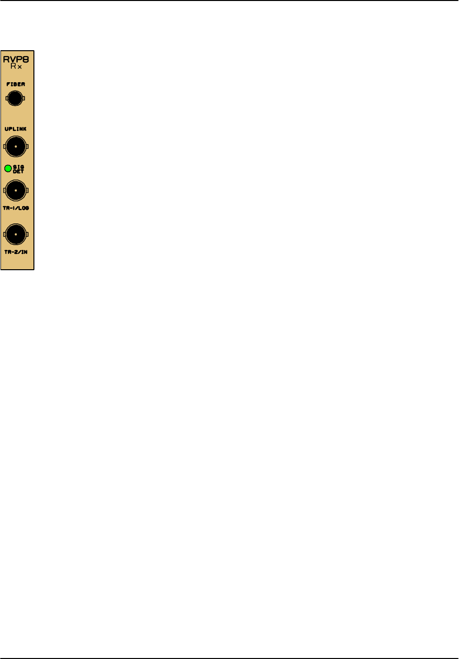
B.1.1 Main Chassis Front Panel B–7 . . . . . . . . . . . . . . . . . . . . . . . . . . . . . . . . . . . .
B.1.2 Main Chassis Back Panel B–8 . . . . . . . . . . . . . . . . . . . . . . . . . . . . . . . . . . . .
B.1.3 Main Chassis Back Panel Power Section B–9 . . . . . . . . . . . . . . . . . . . . . . . .
B.1.4 Main Chassis Back Panel PC I/O Section B–10 . . . . . . . . . . . . . . . . . . . . . . .
B.1.5 Main Chassis Back Panel PCI Card Section B–11 . . . . . . . . . . . . . . . . . . . . .
B.2 I/O-62 and Connector Panel B–12 . . . . . . . . . . . . . . . . . . . . . . . . . . . . . . . . . . . . . . . .
B.3 IFD Module (RVP8 Only) B–28 . . . . . . . . . . . . . . . . . . . . . . . . . . . . . . . . . . . . . . . . .
B.4 DAFC Module (RVP8 only) B–31 . . . . . . . . . . . . . . . . . . . . . . . . . . . . . . . . . . . . . . .
C. Clutter Filter Characteristics (DRAFT) C–1 . . . . . . . . . . . . . . . . . . . . . . . .
D. References and Credits D–1 . . . . . . . . . . . . . . . . . . . . . . . . . . . . . . . . . . . . . .

Table of Contents
RVP8 User’s Manual
12 May 2003
vii
E. Installation and Test Procedure (DRAFT) E–1 . . . . . . . . . . . . . . . . . . . . . . .
E.1 Installation Check E–3 . . . . . . . . . . . . . . . . . . . . . . . . . . . . . . . . . . . . . . . . . . . . . . . .
E.2 Power-Up Check E–4 . . . . . . . . . . . . . . . . . . . . . . . . . . . . . . . . . . . . . . . . . . . . . . . .
E.3 Setup Terminal E–5 . . . . . . . . . . . . . . . . . . . . . . . . . . . . . . . . . . . . . . . . . . . . . . . . . .
E.4 Setup “V” Command (Internal Status) E–6 . . . . . . . . . . . . . . . . . . . . . . . . . . . . . . . .
E.5 Setup “Mc” Command (Board Configuration) E–7 . . . . . . . . . . . . . . . . . . . . . . . . .
E.6 Setup “Mp” Command (Processing Options) E–8 . . . . . . . . . . . . . . . . . . . . . . . . . .
E.7 Setup “Mf” Command (Clutter Filters) E–9 . . . . . . . . . . . . . . . . . . . . . . . . . . . . . . .
E.8 Setup “Mt” Command (General Trigger Setup) E–10 . . . . . . . . . . . . . . . . . . . . . . . .
E.9 Initial Setup of Information for Each Pulse Width E–11 . . . . . . . . . . . . . . . . . . . . . .
E.10 Setup “Mb” Command (Burst Pulse and AFC) E–12 . . . . . . . . . . . . . . . . . . . . . . . .
E.11 Setup “M+” Command (Debug Options) E–13 . . . . . . . . . . . . . . . . . . . . . . . . . . . . .
E.12 Setup “Mz” Command (Transmitter Phase Control) E–14 . . . . . . . . . . . . . . . . . . . .
E.13 Display Scope Test E–15 . . . . . . . . . . . . . . . . . . . . . . . . . . . . . . . . . . . . . . . . . . . . . .
E.14 Burst Pulse Alignment E–16 . . . . . . . . . . . . . . . . . . . . . . . . . . . . . . . . . . . . . . . . . . .
E.15 Bandwidth Filter Adjustment E–17 . . . . . . . . . . . . . . . . . . . . . . . . . . . . . . . . . . . . . .
E.16 Digital AFC Voltage Alignment (Optional) E–18 . . . . . . . . . . . . . . . . . . . . . . . . . . .
E.17 Analog AFC Voltage Alignment (Optional) E–19 . . . . . . . . . . . . . . . . . . . . . . . . . .
E.18 MFC Functional Test and Tuning (Optional) E–21 . . . . . . . . . . . . . . . . . . . . . . . . . .
E.19 AFC Functional Test (Optional) E–22 . . . . . . . . . . . . . . . . . . . . . . . . . . . . . . . . . . . .
E.20 Input IF Signal Level Check E–23 . . . . . . . . . . . . . . . . . . . . . . . . . . . . . . . . . . . . . .
E.21 Dynamic Range Check E–24 . . . . . . . . . . . . . . . . . . . . . . . . . . . . . . . . . . . . . . . . . . .
E.22 Receiver Bandwidth Check E–26 . . . . . . . . . . . . . . . . . . . . . . . . . . . . . . . . . . . . . . .
E.23 Receiver Phase Noise Check E–28 . . . . . . . . . . . . . . . . . . . . . . . . . . . . . . . . . . . . . .
E.24 Hardcopy of Final Setups E–29 . . . . . . . . . . . . . . . . . . . . . . . . . . . . . . . . . . . . . . . . .
E.25 IFD Stand-alone SigGen Bench Test E–30 . . . . . . . . . . . . . . . . . . . . . . . . . . . . . . . .
Index Index–1 . . . . . . . . . . . . . . . . . . . . . . . . . . . . . . . . . . . . . . . . . . . . . . . . . . . .

Table of Contents
RVP8 User’s Manual
12 May 2003
viii
Figures
Figure 1–1: Analog vs Digital Receiver for Magnetron Systems 1–19 . . . . . . . . . . . . . .
Figure 1–2: Analog vs Digital Receiver for Klystron Systems 1–20 . . . . . . . . . . . . . . . .
Figure 1–3: IF to I/Q Processing Steps 1–23 . . . . . . . . . . . . . . . . . . . . . . . . . . . . . . . . . .
Figure 1–4: I/Q Processing for Weather Moment Extraction 1–26 . . . . . . . . . . . . . . . . .
Figure 2–1: Calibration Plot for a Stand-alone 14-Bit IFD 2–10 . . . . . . . . . . . . . . . . . . .
Figure 2–2: Tradeoff Between Dynamic Range and Sensitivity 2–11 . . . . . . . . . . . . . . .
Figure 2–3: Assembly Diagram of the DAFC 2–27 . . . . . . . . . . . . . . . . . . . . . . . . . . . . .
Figure 2–4: Recommended Receiving Circuit for the Coax Uplink 2–32 . . . . . . . . . . . .
Figure 2–5: Timing Diagram of the IFD Coax Uplink 2–33 . . . . . . . . . . . . . . . . . . . . . .
Figure 2–6: Timing diagram of the (I,Q) Data Stream 2–36 . . . . . . . . . . . . . . . . . . . . . .
Figure 4–1: Oscilloscope Display of Test Pattern 4–3 . . . . . . . . . . . . . . . . . . . . . . . . . .
Figure 4–2: Successful Capture of the Transmit Burst 4–6 . . . . . . . . . . . . . . . . . . . . . .
Figure 4–3: Example of a Filter With Excellent DC Rejection 4–11 . . . . . . . . . . . . . . . .
Figure 4–4: Example of a Poorly Matched Filter 4–20 . . . . . . . . . . . . . . . . . . . . . . . . . .
Figure 4–5: Example of a Filter With Poor DC Rejection 4–22 . . . . . . . . . . . . . . . . . . .
Figure 4–6: Example of Combined IF Sample and LOG Plot 4–23 . . . . . . . . . . . . . . . .
Figure 4–7: Example of a Noisy High Resolution “Pr” Spectrum 4–25 . . . . . . . . . . . . .
Figure 5–1: Flow Diagram of RVP8 Processing 5–3 . . . . . . . . . . . . . . . . . . . . . . . . . . .
Figure 5–2: Linearization of Saturated Signals Above +4dBm 5–10 . . . . . . . . . . . . . . .
Figure 5–3: Model Intensity Curve 5–25 . . . . . . . . . . . . . . . . . . . . . . . . . . . . . . . . . . . . .
Figure 5–4: Illustration of Losses that Affect LOG Calibration 5–28 . . . . . . . . . . . . . . .
Figure 5–5: Dual PRF Concepts 5–33 . . . . . . . . . . . . . . . . . . . . . . . . . . . . . . . . . . . . . . .
Figure 5–6: Example of Dual PRF Trigger Waveforms 5–35 . . . . . . . . . . . . . . . . . . . . .
Figure 5–7: Dual Receiver Magnetron Case 5–40 . . . . . . . . . . . . . . . . . . . . . . . . . . . . . .
Figure 5–8: Comparison of Pulse Pair and FFT Clutter Filters 5–64 . . . . . . . . . . . . . . .
Figure 5–9: FFT Processing — 50 pulse example 5–66 . . . . . . . . . . . . . . . . . . . . . . . . .
Figure 5–10: Effect of Windowing on FFT Response to Ground Clutter 5–67 . . . . . . . .
Figure 5–11: Example of FFT Clutter Filter in Frequency Domain 5–68 . . . . . . . . . . . .
Figure 5–12: Random Phase Processing Algorithm 5–74 . . . . . . . . . . . . . . . . . . . . . . . .
Figure B–1: Main Chassis- Front Panel B–3 . . . . . . . . . . . . . . . . . . . . . . . . . . . . . . . . . .
Figure B–2: Main Chassis- Back Panel B–4 . . . . . . . . . . . . . . . . . . . . . . . . . . . . . . . . . .
Figure B–3: Main Chassis- Right Side View B–5 . . . . . . . . . . . . . . . . . . . . . . . . . . . . . .
Figure B–4: Main Chassis Internal Cabling B–6 . . . . . . . . . . . . . . . . . . . . . . . . . . . . . .
Figure B–5: RVP8 I/O-62 Connector Panel B–14 . . . . . . . . . . . . . . . . . . . . . . . . . . . . . .
Figure B–6: RCP8 I/O-62 Connector Panel B–15 . . . . . . . . . . . . . . . . . . . . . . . . . . . . . .
Figure B–7: RVP8/IFD Module B–29 . . . . . . . . . . . . . . . . . . . . . . . . . . . . . . . . . . . . . . . .
Figure B–8: IFD Front Panel B–30 . . . . . . . . . . . . . . . . . . . . . . . . . . . . . . . . . . . . . . . . . .
Figure B–9: View of DAFC Module B–31 . . . . . . . . . . . . . . . . . . . . . . . . . . . . . . . . . . . .
Figure C–1: 40 dB IIR Clutter Filter Responses C–3 . . . . . . . . . . . . . . . . . . . . . . . . . . .
Figure C–2: 50 dB IIR Clutter Filters Responses C–4 . . . . . . . . . . . . . . . . . . . . . . . . . .

Table of Contents
RVP8 User’s Manual
12 May 2003
ix
Tables
Table 1–1: Examples of Dual PRF Velocity Unfolding 1–28 . . . . . . . . . . . . . . . . . . . . .
Table 2–1: Differences Among Versions of the IFD 2–3 . . . . . . . . . . . . . . . . . . . . . . . .
Table 2–2: IFD I/O Connections 2–5 . . . . . . . . . . . . . . . . . . . . . . . . . . . . . . . . . . . . . . .
Table 2–3: IFD Toggle Switch Settings 2–6 . . . . . . . . . . . . . . . . . . . . . . . . . . . . . . . . . .
Table 2–4: IFD LED Indicator Interpretations 2–6 . . . . . . . . . . . . . . . . . . . . . . . . . . . .
Table 2–5: IFD Internal Jumper Settings 2–7 . . . . . . . . . . . . . . . . . . . . . . . . . . . . . . . . .
Table 2–6: Direct Connections to RVP8 Main Chassis 2–19 . . . . . . . . . . . . . . . . . . . . . .
Table 2–7: DAFC Protocol Jumper Selections 2–28 . . . . . . . . . . . . . . . . . . . . . . . . . . . .
Table 2–8: Pinout for the CTI “MVSR-xxx” STALO 2–30 . . . . . . . . . . . . . . . . . . . . . . .
Table 2–9: Bit Assignments for the IFD Coax Uplink 2–33 . . . . . . . . . . . . . . . . . . . . . .
Table 5–1: Algebraic Quantities Within the RVP8 Processor 5–2 . . . . . . . . . . . . . . . . .
Table 5–2: Algorithm Results for +16dB Interference 5–8 . . . . . . . . . . . . . . . . . . . . . .
Table 5–3: Algorithm Results for +26dB Interference 5–9 . . . . . . . . . . . . . . . . . . . . . .
Table 6–2: RVP8 Status Output Words 6–22 . . . . . . . . . . . . . . . . . . . . . . . . . . . . . . . . .
Table B–1: J1 “AZ INPUT” B–16 . . . . . . . . . . . . . . . . . . . . . . . . . . . . . . . . . . . . . . . . . .
Table B–2: J2 “AZ OUTPUT” B–17 . . . . . . . . . . . . . . . . . . . . . . . . . . . . . . . . . . . . . . . .
Table B–3: J3 RVP8: “PHASE OUT”; RCP8 “CONTROL” B–18 . . . . . . . . . . . . . . . . .
Table B–4: J4 “EL INPUT” B–19 . . . . . . . . . . . . . . . . . . . . . . . . . . . . . . . . . . . . . . . . . . .
Table B–5: J5 “EL OUTPUT” B–20 . . . . . . . . . . . . . . . . . . . . . . . . . . . . . . . . . . . . . . . . .
Table B–6: J6 “RELAY” B–21 . . . . . . . . . . . . . . . . . . . . . . . . . . . . . . . . . . . . . . . . . . . . .
Table B–7: J7: RVP8 “SPARE”; RCP8 “BITE 19:0” B–22 . . . . . . . . . . . . . . . . . . . . . . .
Table B–8: J8: RVP8 “SPARE”; RCP8 “ANALOG IN” B–23 . . . . . . . . . . . . . . . . . . . . .
Table B–9: J9 RVP8: “MISC I/O” ; RCP8: “PED/STATUS” B–24 . . . . . . . . . . . . . . . . .
Table B–10: J10 “SERIAL” B–25 . . . . . . . . . . . . . . . . . . . . . . . . . . . . . . . . . . . . . . . . . . .
Table B–11: J11 “SERIAL” B–25 . . . . . . . . . . . . . . . . . . . . . . . . . . . . . . . . . . . . . . . . . . .
Table B–12: J12 “S–D” B–26 . . . . . . . . . . . . . . . . . . . . . . . . . . . . . . . . . . . . . . . . . . . . . .
Table B–13: RVP8 BNC Connector Pin Assignments B–27 . . . . . . . . . . . . . . . . . . . . . .
Table B–14: RCP8 BNC Connector Pin Assignments B–27 . . . . . . . . . . . . . . . . . . . . . .
Table C–1: Doppler 40dB Clutter Filter Coefficients C–1 . . . . . . . . . . . . . . . . . . . . . .
Table C–2: Doppler 50dB Clutter Filter Coefficients C–2 . . . . . . . . . . . . . . . . . . . . . .

Preface
RVP8 User’s Manual
April 2003
x
Hardware Limited Warranty
SIGMET, Inc. warrants its IRIS hardware (RVP8 and RCP8) to function according to the
hardware User’s Manual documentation for a period of one year following delivery. In the event
of a failure during the warranty period, the customer should notify SIGMET to obtain a Return
Authorization. Upon receiving the Return Authorization from SIGMET, the customer ships the
failed unit to SIGMET by pre-paid freight. SIGMET, at its option, will repair or replace the
defective unit within 30 days and return the unit to the customer.
Damage caused by fire, flood, lightning, or other catastrophe, and damage caused by misuse or
abuse are not covered by this warranty.
In no event shall SIGMET, Inc. be liable for any direct, indirect, special, incidental, or
consequential damages arising out of the use or inability to use the hardware or
documentation provided by SIGMET, Inc. SIGMET, Inc. makes no warranty, either
express or implied, with respect to any of the hardware or documentation, as to the quality,
performance, merchantability, or fitness for a particular purpose.

Preface
RVP8 User’s Manual
April 2003
xi
Preface
This manual provides technical information on the RVP8 digital receiver and Doppler signal
processor.
About This Manual
This manual is used primarily by engineers for installation and troubleshooting, or by users
interested in understanding the signal processing features, algorithms, and control and data
formats.
Chapter 1, Introduction and Specifications, describes the major features of the RVP8 signal
processor and gives its technical specifications.
Chapter 2, Hardware Installation, discusses the electrical issues involved with installing the
RVP8 processor and IFD receiver module. This includes power supply connections, radar
analog and digital signal interfaces and computer interface connections. Software installation is
covered in a separate Appendix.
Chapter 3, TTY Nonvolatile Setups, continues the installation discussion by describing how to
use the local TTY to configure the actual operation of the RVP8. This includes a detailed
description of the (approximately one hundred) setup parameters that affect the operation of the
RVP8.
Chapter 4, Plot-Assisted Setups, completes the installation discussion by using the oscilloscope
plotting modes to configure and align the radar receiver, and measure its performance.
Chapter 5, Processing Algorithms, gives mathematical descriptions of the processing algorithms
implemented in the RVP8 signal processor. This information can be useful to those writing their
own interface to the RVP8, or for those who want to learn more about the internal workings of
the signal processor.
Chapter 6, Host Computer Commands, contains a description of the digital commands that the
host computer must use to set up and control the RVP8 processor. The introductory section
discusses processor I/O in general, and gives an overview of how to set up the RVP8 for
recording data. Each command is then detailed in subsequent sections.
The appendixes give information on software installation and backup, the RVP8 standard
chassis, and clutter filter characteristics.

Preface
RVP8 User’s Manual
April 2003
xii
Where to Find More Information
The following manuals are also available from SIGMET, Inc.:
IRIS
Installation Manual Describes the procedures for installing and upgrading IRIS and
the specific hardware and software configuration for your
facility.
IRIS
Radar Manual
Describes the IRIS/Radar software. This manual is for radar
operators.
IRIS
Product & Display Manual Describes the IRIS/Analysis product generation software and the
IRIS/Display software.
IRIS
Utilities Manual Describes the utility programs for system alignment, calibration,
installation and testing.
IRIS
Programmer’s Manual Describes the data formats and library routines used by IRIS.
This manual is for programmers who want to access IRIS data or
interface to IRIS processes.
The RCP8
User’s Manual Describes the installation, operation and technical details of the
Radar Control Processor. The RCP8 is an interface between the
IRIS software and miscellaneous hardware such as the antenna
and transmitter.
SIGMET, Inc. encourages you to send your comments and/or corrections to:
SIGMET, Inc.
2 Park Drive, Suite 1
Westford, Massachusetts 01886
USA
FAX (978)692–9575
EMAIL support@sigmet.com
Documentation Conventions
The following conventions are used throughout this manual:
prompt Some features of the RVP8 operate by displaying questions and
waiting for you to type an answer. The text of prompts is
displayed in bold, monospaced type.
This margin icon indicates a note that may be of interest to the
reader.
This margin icon indicates a note that is important to the reader.
This margin icon indicates a caution or warning to the reader.

Introduction and Specifications
RVP8 User’s Manual
May 2003
1–1
1. Introduction and Specifications
The RVP8 Lineage
SIGMET Inc. has a 20-year history of supplying innovative, high-quality signal processing
products to the weather radar community. The history of SIGMET products reads like a history
of weather radar signal processing:
Year Model Units
Sold Major Technical Milestones
1981 FFT 10 First commercial FFT-based Doppler signal processor for weath-
er radar applications. Featured Simultaneous Doppler and inten-
sity processing.
1985 RVP5 161 First single-board low-cost Doppler signal processor. First com-
mercial application of dual PRF velocity unfolding algorithm.
1986 PP02 12 First high-performance commercial pulse pair processor with
18.75-m bin spacing and 1024 bins.
1992 RVP6 150 First commercial floating-point DSP-chip based processor. First
commercial processor to implement selectable pulse pair, FFT or
random phase 2nd trip echo filtering.
1996 RVP7 >200 First commercial processor to implement fully digital IF process-
ing for weather radar.
2003 RVP8 First digital receiver/signal processor to be implemented using an
open hardware and software architecture on standard PC hard-
ware under the Linux operating system. Public API’s are pro-
vided so that customers may implement their own custom proc-
essing algorithms.
Much of the proven, tested, documented software from the highly-successful RVP7 (written in
C) is ported directly to the new RVP8 architecture. This allows SIGMET to reduce
time-to-market and produce a high-quality, reliable system from day one. However, the new
RVP8 is not simply a re-hosting of the RVP7. The RVP8 provides new capabilities for weather
radar systems that, until now, were not available outside of the research community.
Advanced Digital Transmitter Option
For example, the RVP8 takes the next logical step after a digital receiver- a digitally synthesized
IF transmit waveform output that is mixed with the STALO to provide the RF waveform to the
transmitter amplifier (e.g., Klystron or TWT). The optional RVP8/Tx card opens the door for
advanced processing algorithms such as pulse compression, frequency agility and phase agility
that were not possible before, or done in more costly ways.

Introduction and Specifications
RVP8 User’s Manual
May 2003
1–2
Open Hardware and Software Design
Compared to previous processors that were built around proprietary DSP chips, perhaps the most
innovative aspect of the RVP8 is that it is implemented on standard PC hardware and software
that can be purchased from a wide variety of sources. The Intel Pentium/PCI approach promises
continued improvement in processor speed, bus bandwidth and the availability of low–cost
compatible hardware and peripherals. The performance of an entry level RVP8 (currently dual
2.4 GHz Pentium processors) is 6 times faster than the fastest RVP7 ever produced (with two
RVP7/AUX boards).
Aside from the open hardware approach, the RVP8 has an open software approach as well. The
RVP8 runs in the context of the Linux operating system. The code is structured and public API’s
are provided so that research customers can modify/replace existing SIGMET algorithms, or
write their own software from scratch using the RVP8 software structure as a foundation on
which to build.
The advantage of the open hardware and software PCI approach is reduced cost and the ability
for customers to maintain, upgrade and expand the processor in the future by purchasing
standard, low cost PC components from local sources.
SoftPlane High–Speed I/O Interconnect
There are potentially many different I/O signals emanating from the backpanel of the RVP8.
Most of these conform to well-known electrical and protocol standards (VGA, SCSI, 10–BaseT,
RS-232 Serial, PS/2 Keyboard, etc.), and can be driven by standard commercial boards that are
available from multiple vendors. However, there are other interface signals such as triggers and
clocks that require careful timing. These precise signals cannot tolerate the PCI bus latency. For
signals that have medium–speed requirements (~1 microsec latency) for which the PCI bus is
inappropriate; and others that require a high–speed (~ 1 ns latency) connection that can only be
achieved with a dedicated wire, the RVP8 Softplane provides the solution.
Physically, the Softplane is a 16-wire digital “daisy-chain” bus that plugs into the tops of the
RVP8/Rx, RVP8/Tx, and I/O boards. The wires connect to the FPGA chips on each card, and the
function of each wire is assigned at run–time based on the connectivity needs of the overall
system. The Softplane allocates a dedicated wire to carry each high-speed signal; but groups of
medium-speed signals are multiplexed onto single wires in order to conserve resources. Even
though there are only 16 wires available, the Softplane is able to carry several high-speed signals
and hundreds of medium–speed signals, as long as the total bandwidth does not exceed about
600MBits/sec.
The Softplane I/O is configured at run–time based on a file description rather than custom
wiring such as wirewrap. Neither the PCI backplane nor the physical Softplane are customized
in any way. Since there is no custom wiring, a failed board can be replaced with a generic
off–the–shelf spare, and that spare will automatically resume whatever functions had been
assigned to the original board. Similarly, if the chassis itself were to fail, then simply plugging
the boards into another generic chassis would restore complete operation. Cards and chassis can
be swapped between systems without needing to worry about custom wiring.

Introduction and Specifications
RVP8 User’s Manual
May 2003
1–3
Standard LAN Interconnection for Data Transfer or Parallel Processing
For communication with the outside world, the RVP8 supports as standard a 10/100/1000 Base T
Ethernet. For most applications, the 100 BaseT Ethernet is used to transfer moment results (Z, T,
V, W) to the applications host computer (e.g., a product generator). However, the gigabit
Ethernet is sufficiently fast to allow UDP broadcast of the I and Q values for the purpose of
archiving and/or parallel processing. In other words, a completely separate signal processor can
ingest and process the I and Q values generated by the RVP8.

Introduction and Specifications
RVP8 User’s Manual
May 2003
1–4
1.1 System Configuration Concepts
The hardware building blocks of an RVP8 system are actually quite few in number:
RVP8/IFD IF Digitizer Unit- This is a separate sealed unit usually mounted in
the receiver cabinet. The primary input to the IFD is the received IF signal. In
addition, the IFD has channels to sample the transmit pulse and to take in an
external clock to phase lock the A/D conversion with the transmit pulse (not used
for magnetron systems).
RVP8/Rx Card- A PCI long format card mounted in the chassis. It connects to
the IFD by a fiberoptic downlink and a coax uplink which can be up to 100m
distant. In addition, there are two BNC trigger input/output (programmable).
I/O-62 Card and Connector Panel- These handle all of the various I/O
associated with a radar signal processor, such as triggers, antenna angles,
polarization switch controls, pulse width control, etc. The Connector Panel is
mounted on either the front or rear of the equipment rack and a cable (supplied)
connects the panel to the I/O-62.
Optional RVP8/Tx card- This supplies two IF output signals with
programmable frequency, phase and amplitude modulation. In the simplest case,
it supplies the COHO which is then mixed up with the STALO to generate the
transmit RF for Klystron or TWT systems. This card is not necessary for
magnetron systems.
PC Chassis and Processor with various peripherals- a robust 6U rack mount
unit with either a mother board or single board computer (SBC) in a passive back
plane. There is a diagnostic front panel display, disk (mechanical or flash),
CDRW, keyboard, mouse and optional monitor for local diagnostic work. Dual or
tri–redundant power supplies are used and there are redundant fans as well.
This modular hardware approach allows the various components to be mixed and matched to
support applications ranging from a simple magnetron system to an advanced dual polarization
system with pulse compression. Typically SIGMET supplies turn-key systems, although some
OEM customers who produce many systems purchase individual components and integrate them
by themselves. This allows OEM customers to put their own custom “stamp” on the processor
and even their own custom software if they so choose.
For the turnkey systems provided by SIGMET, the basic chassis is a 6U rackmount unit as
described above. A 2U chassis can be provided for applications for which space is limited. A
very low cost approach is to use a desk side PC, but this is not recommended for applications
that require long periods of unattended operation.
To illustrate various RVP8 configurations, some typical examples are shown below. For clarity,
all the examples show the single–board computer approach. A mother board approach is
equivalent.
Introduction and Specifications
RVP8 User’s Manual
May 2003
1–5
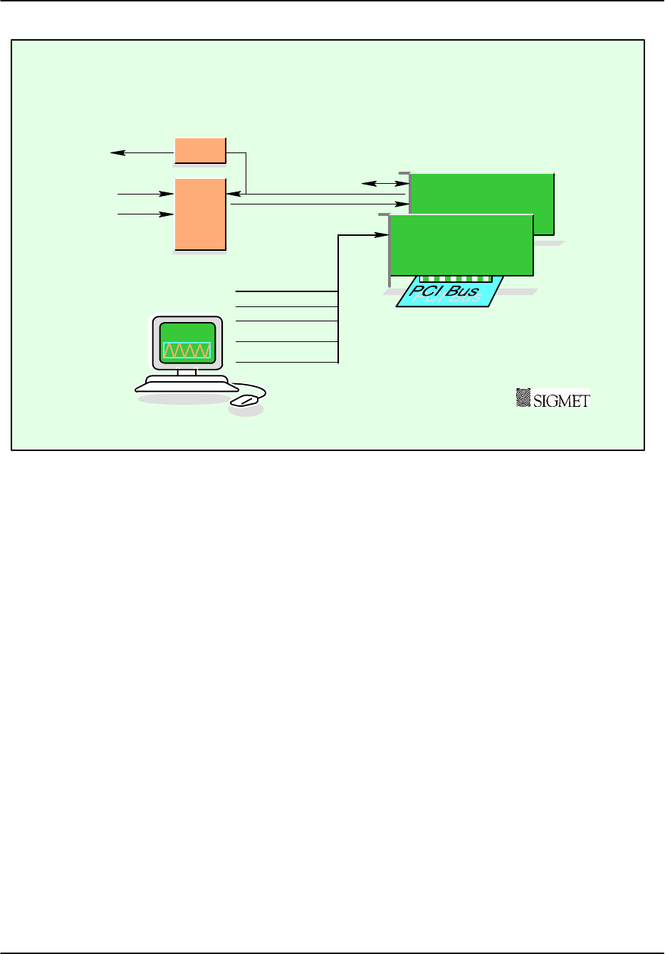
Keyboard
Mouse
Monitor
10/100 BaseT LAN Interface
IFD Fiber Downlink
COAX Uplink
RS232C Antenna Angles
RVP8 Configuration Example: Basic Magnetron System
Triggers
IF Signal
IF Magnetron Burst
DAFCDigital STALO
Optional
Utilities
14-Bit
SBC
RVP8/Rx
Example 1: Basic Magnetron System
The building blocks required to construct the basic system are:
IFD- IF Digitizer installed in the radar receiver cabinet. This can be located up to 100
meters from the RVP8 main chassis (fiber optic connection). The DAFC (Digital AFC) is
an option to interface to a digitally controlled STALO. Like the RVP7, the RVP8
provides full AFC with burst pulse auto-tracking.
RVP8/Rx- The digital receiver collects digitized samples from the IFD and does the
processing to obtain I/Q. It also provides two trigger connections configurable for input
or output.
SBC Card- Single Board Computer with dual SMP processors (PC) running Linux.
The figure above shows a basic magnetron system constructed with an IFD, and two PCI cards.
A standard RS-232 serial input (included with the SBC) is used for obtaining the antenna angles
and the output/input trigger is provided directly from the Rx card. This system has 5 times the
processing power of the fastest version of the previous generation processor (RVP7/Main board
plus 2 RVP7/AUX boards) so that it is capable of performing DFT processing in 2048 rangebins
with advanced algorithms such as random phase 2nd trip echo filtering and recovery.
Introduction and Specifications
RVP8 User’s Manual
May 2003
1–6
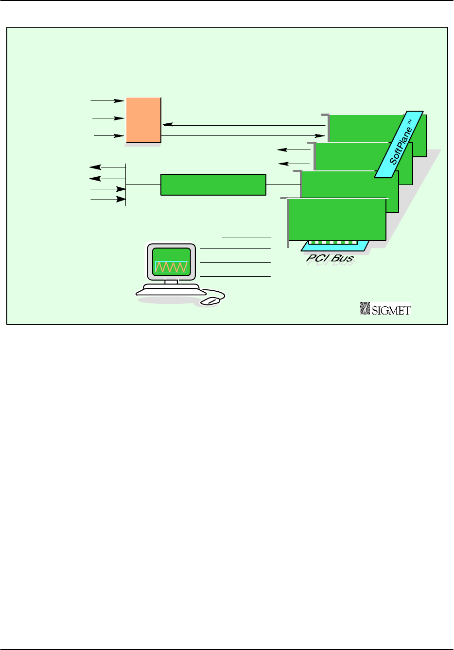
RVP8 Configuration Example: High Performance Klystron
Keyboard
Mouse
Monitor
10/100/1000 Base T
IFD
Fiber Downlink
COAX Uplink
Triggers
IF Signal
Reference Clock
Digitally Synthesized COHO
Parallel or Synchro AZ
Parallell or Synchro EL
Pulse width IF Tx Waveform
Utilities
IF Tx Waveform
14-Bit
I/O62
SBC
RVP8/Tx
RVP8/Rx
Connector Panel
Example 2: Klystron System with Digital Tx
In this case, the IFD can receive a master clock from the radar system (e.g., the COHO). This
ensures that the entire system is phase locked. As compared to the previous example there are
two additional cards shown in this example:
RVP8/Tx- The digital transmitter card provides the digital Tx waveform. A second
output can be used to provide a COHO in the event that the RVP8 is used to provide the
system master clock. In any case, the IF transit waveform and the A/D sampling are
phase locked.
SIGMET I/O-62 card for additional triggers, parallel, synchro or encoder AZ and EL
angle inputs, pulse width control, spot blanking control output, etc. These signals are
brought in via the connector panel.
The figure shows the SIGMET SoftPlane which carries time-critical I/O such as clock and
trigger information which is not appropriate for the PCI bus. These signals are limited to the
cards provided by SIGMET, i.e., the SoftPlane is not connected to any of the standard
commercial cards.
Introduction and Specifications
RVP8 User’s Manual
May 2003
1–7
IFD
Fiber Downlink
COAX Uplink
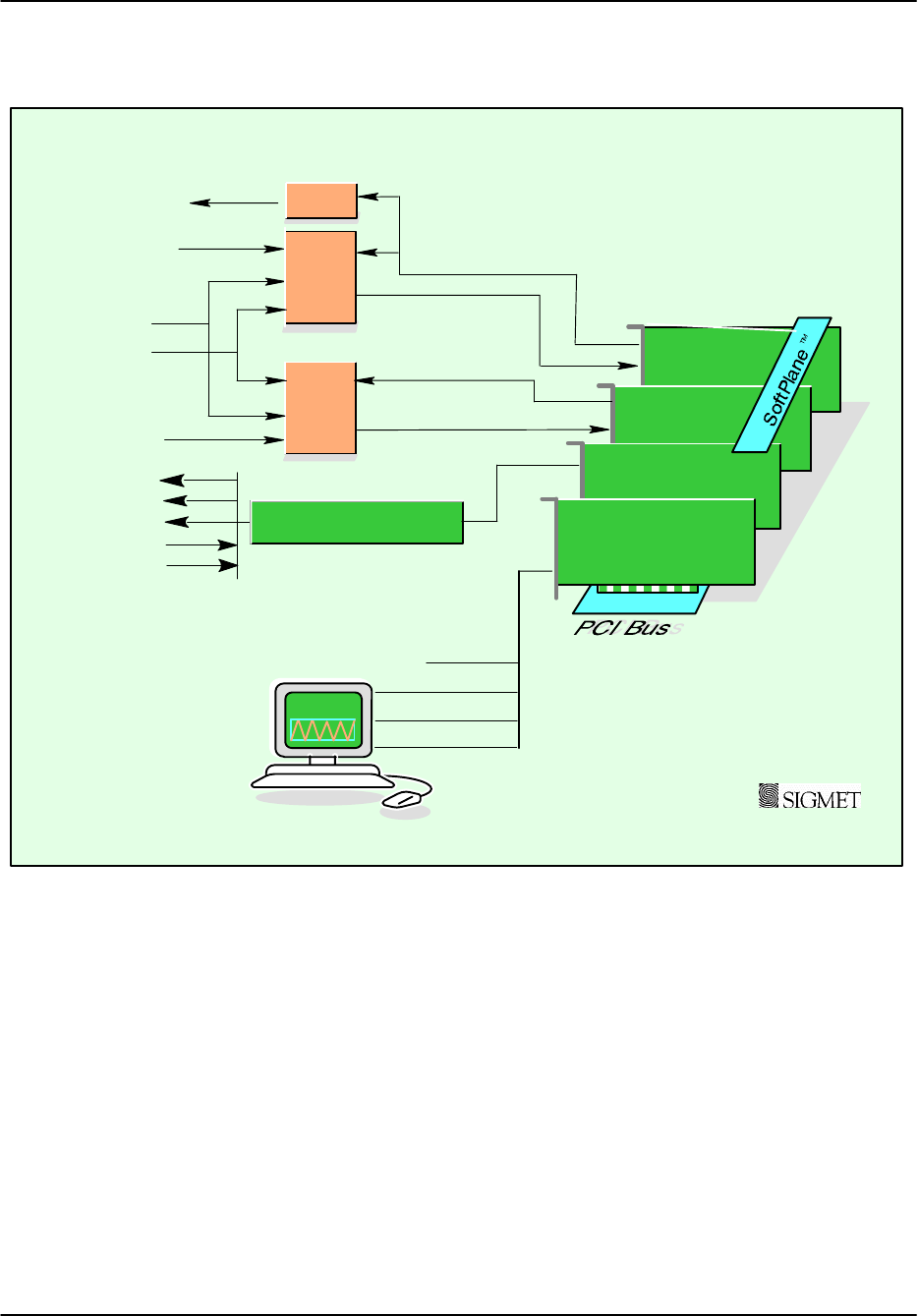
RVP8 Configuration Example: Dual Polarization Magnetron System
Keyboard
Mouse
Monitor
10/100/1000 BaseT LAN
IFD
Horizontal IF Signal
DAFCDigital STALO
Optional
Vertical IF Signal
Utilities
14-Bit
14-Bit
IF Magnetron Burst
Synch Clock
Fiber Downlink
Horz
Vert I/O62
SBC
RVP8/Rx
RVP8/Rx
COAX Uplink
Triggers
Parallel or Synchro AZ
Parallell or Synchro EL
Pulse Width Control
Connector Panel
Polarization Control
Example 3: Dual Polarization Magnetron System
In this system 2 IFD’s and two RVP8/Rx cards are used for the horizontal and vertical channels
of a dual-channel receiver. The legacy RVP7 technique of using a single IFD and two IF
frequencies for the horizontal and vertical channels (e.g., 24 and 30 MHz) is also supported by
the RVP8. In the case of either dual or single IFD’s, there is a synch clock provided by either the
STALO reference frequency (e.g., 10 MHz) or by the RVP8 itself.
The RVP8 supports calculation of the complete covariance matrix for dual pol, including ZDR,
PHIDP (KDP), RHOHV, LDR, etc. Which of these variables is available depends on whether the
system is a single–channel switching system (alternate H and V), a STAR system (simultaneous
transmit and receive) or a dual channel switching system (co and cross receivers). Note that for
the special case of a single channel switching system, only one IFD is required.

Introduction and Specifications
RVP8 User’s Manual
May 2003
1–8
COTS Accessories
Aside from the basic PCI cards required for the radar application, there are additional cards that
can be installed to meet different customer requirements, e.g.,
10/100–BaseT Ethernet card for additional network I/O (e.g., a backup network).
RS-232/RS-422 serial cards for serial angles, remote TTY control, etc.
Sound card to synthesize audio waveforms for wind profiler applications.
GPS card for time synch.
IEEE 488 GPIB card for control of test equipment.
The bottom line is that the PCI open hardware approach provides unparalleled hardware
flexibility. In addition, the availability of compatible low-cost replacement or upgrade parts is
assured for years into the future.
Introduction and Specifications
RVP8 User’s Manual
May 2003
1–9
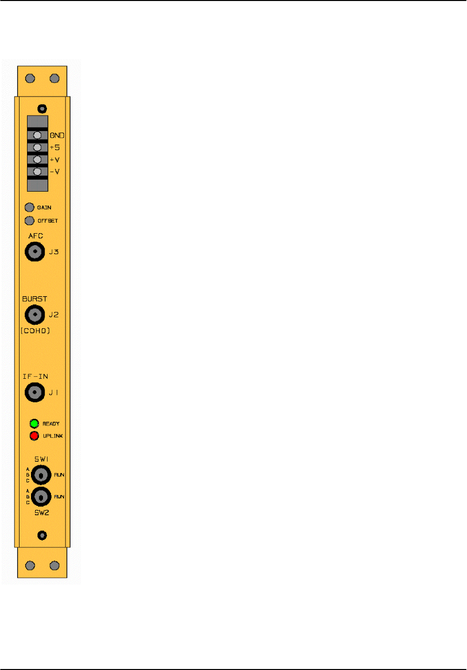
1.1.1 IFD IF Digitizer
The IFD 14–bit IF digitizer is a totally sealed unit for optimum low–noise per-
formance. The use of digital components within the IFD is minimized and the
unit is carefully grounded and shielded to make the cleanest possible digital
capture of the input IF signal. Because of this, the IFD achieves the theoretical
minimum noise level for the A/D convertors.
There are 3 inputs to the IFD:
IF signal in the nominal ranges of 20 -34, 38-52 and 56-70 MHz. The user
simply enters the system IF frequency as a setup parameter.
IF Burst Pulse for magnetron or IF COHO for Klystron.
Optional reference clock for system synchronization. For a Klystron system,
the COHO can be input. Magnetron systems do not require this signal. This
clock can even come from the RVP8/Tx card itself.
All of these inputs are on SMA connectors. The IF signal input is made imme-
diately after the STALO mixing/sideband filtering step of the receiver where
a traditional log receiver would normally be installed. The required signal lev-
el for both the IF signal and burst is +6.5 dBm for the strongest expected input
signal. A fixed attenuator or IF amplifier may be used to adjust the signal level
to be in this range.
Digitizing is performed for both the IF signal and burst/COHO channels at
approximately 36 MHz to 14–bits. This provides 92 to 102 dB of dynamic
range (depending on pulse width) without using complex AGC, dual A/D
ranging or down mixing to a lower IF frequency.
The uplink from the RVP8/Rx is an SMA input on 75–Ohm shielded cable.
This carries timing and AFC information back to the IFD. The data downlink
to the RVP8/Rx card is a fiber optic cable. The IFD may be separated from
the Rx Board by up to 100 meters.
The RVP8 provides comprehensive AFC support for tuning the STALO of a magnetron system.
Alternatively, the magnetron itself can be tuned by a motorized tuning circuit controlled by the
RVP8. Both analog (+–10V) and digital tuning (with optional DAFC to 24 bits) are supported.
Introduction and Specifications
RVP8 User’s Manual
May 2003
1–10
1.1.2 Digital Receiver PCI Card (RVP8/Rx)
The RVP8/Rx card receives the digitized IF samples from the IFD via the fiber optic
link. The advantage of this design is that the receiver electronics (LNA, RF mixer,
IF preamp, and IFD) can be located as far as 100–meters away from the RVP8 main
chassis. This makes it possible to choose optimum locations for both the IFD and the
RVP8, e.g., the IFD could be mounted on the antenna itself, and the processor box
in a nearby equipment room.
The RVP8/Rx is 100% compatible with the 14–bit RVP7/IFD, but it also includes
hooks for future IFD’s operating at higher sampling clock rates. Two additional BNC
connectors are included on the board’s faceplate. These can be used for trigger input,
programmable trigger output, or a simple LOG analog ascope waveform.
A remarkable amount of computing power is resident on the receiver board, in the
form of an FIR filter array that can execute 6.9 billion multiply/accumulate cycles
per second. These chips serve as the first stage of processing of the raw IF data sam-
ples. Their job is to perform the down–conversion, bandpass, and deconvolution
steps that are required to produce (I,Q) time series. The time series data are then trans-
ferred over the PCI bus to the SBC for final processing.
The FIR filter array can buffer as much as 80 microsec of 36MHz IF samples, and then compute
a pair of 2880–point dot products on those data every 0.83 microsec. This could be used to
produce over-sampled (I,Q) time series having a range resolution of 125–meters and a
bandwidth as narrow as 30Khz. The same computation could also yield independent 125–meter
time series data from an 80 microsec compressed pulse whose transmit bandwidth was
approximately 1MHz.
Finer range resolutions are also possible, down to a minimum of 25–meters. A special feature of
the RVP8/Rx is that the bin spacing of the (I,Q) data can be set to any desired value between 25
and 2000 meters. Range bins are placed accurately to within +2.2 meters of any selected grid,
which does not have to be an integer multiple of the sampling clock. However, when an integer
multiple (N x 8.333–meters) is selected, the error in bin placement effectively drops to zero.
Dual polarization radars that are capable of simultaneous reception for both horizontal and
vertical channels can be interfaced to the RVP8 using a separate RVP8/Rx and IFD for each
channel. Note that the multiplexed dual IF approach used for the RVP7 with a single IFD can
also be used.
One of the primary advantages of the digital receiver approach is that wide linear dynamic range
can be achieved without the need for complex AGC circuits that require both phase and
amplitude calibration.
Introduction and Specifications
RVP8 User’s Manual
May 2003
1–11
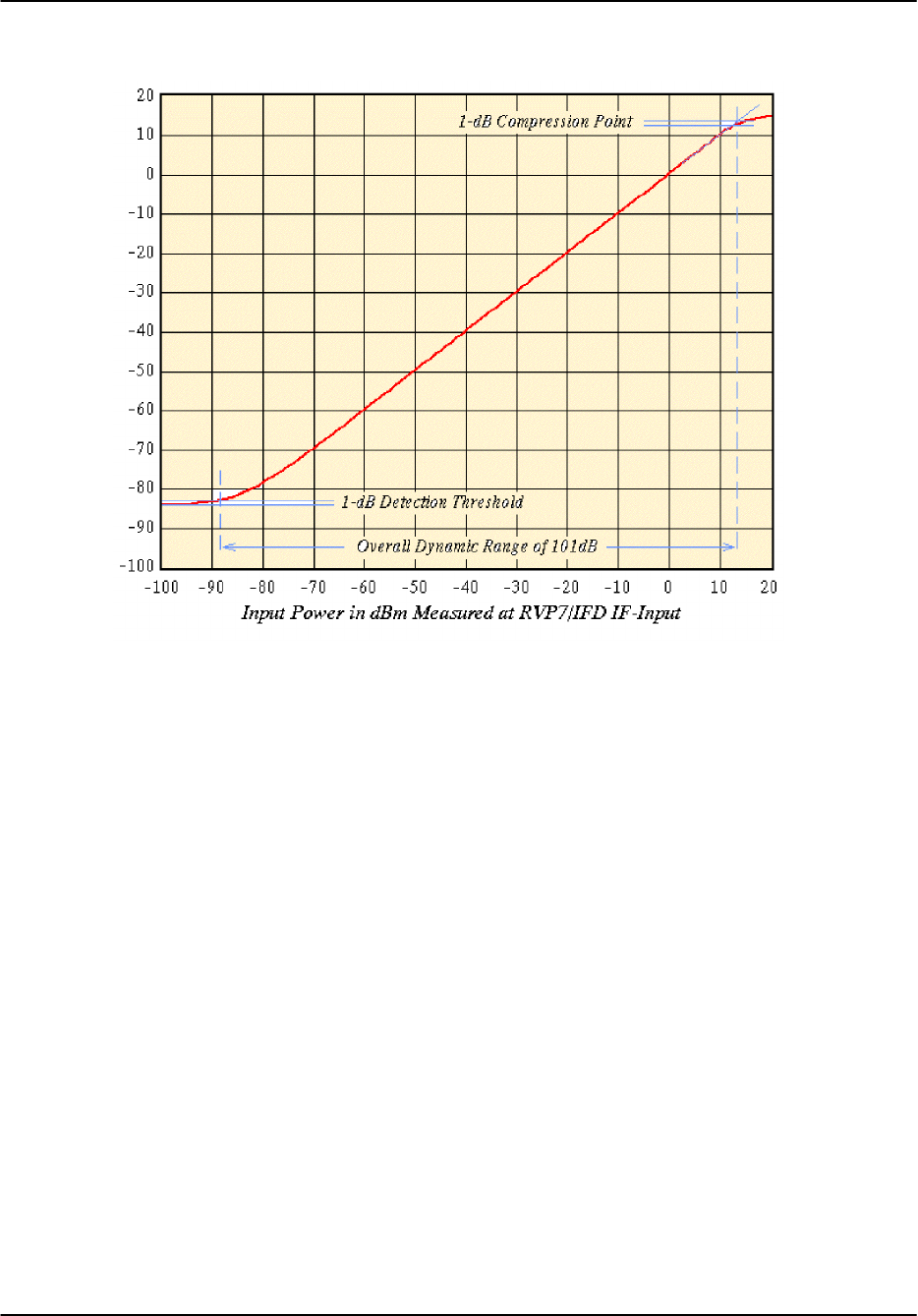
Calibration Plot for RVP8/IFD
The figure above shows a calibration plot for a 14–bit IFD with the digital filter matched to a 2
microsecond pulse. The performance in this case is >100 dB dynamic range– fully linear.
The RVP8 performs several real time signal corrections to the I/Q samples from the Rx,
including:
Amplitude Correction- A running average of the transmit pulse power in the magnetron burst
channel is computed in real-time by the RVP8/Rx. The individual received I/Q samples are
corrected for pulse–to–pulse deviations from this average. This can substantially improve the
“phase stability” of a magnetron system to improve the clutter cancelation performance to near
Klystron levels.
Phase Correction- The phase of the transmit waveform is measured for each pulse (either the
burst pulse for magnetron systems or the Tx Waveform for coherent systems). The I/Q values
are adjusted for the actual measured phase. The coherency achievable is better than 0.1 degrees
by this technique.
Large Signal Linearization- When an IF signal saturates, there is still considerable information
in the signal since only the peaks are clipped. The proprietary large signal linearization
algorithm used in the RVP8 provides an extra 3 to 4 dB of dynamic range by accounting for the
effects of saturation.
The RVP8/Rx card provides the same comprehensive configuration and test utilities as the
RVP7, with the difference that no external host computer is required to run the utilities. These
utilities can be run either locally or remotely– over the network! Some examples are shown
below:
Introduction and Specifications
RVP8 User’s Manual
May 2003
1–12
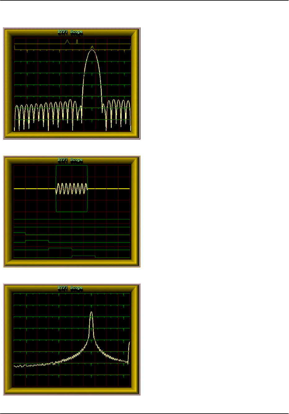
Digital IF Band Pass Design Tool
The built–in filter design tool makes it easy for
anyone to design the optimal IF filter to match
each pulse width and application. Simply specify
the impulse response and pass band and the filter
appears. The user interface makes it easy to wid-
en/narrow the filter with simple keyboard com-
mands. There is even a command to automatical-
ly search for an optimal filter.
This display can also show the actual spectrum
of the transmit burst pulse for quality control and
comparison with the filter.
Burst Pulse Alignment Tool
The quality assessment of the transmit burst
pulse and its precise alignment at range zero
are easy to do, either manually using this tool
and/or automatically using the burst pulse
auto-track feature. This performs a 2D search
in both time and frequency space if a valid
burst pulse is not detected. The automatic
tracking makes the AFC robust to start–up
temperature changes and pulse width changes
that can effect the magnetron frequency.
AFC alignment/check is now much easier
since it can be done manually from a central
maintenance site or fully automatically.
Received Signal Spectrum Analysis Tool
The RVP8 provides plots of the IF signal versus
range as well as spectrum analysis of the signal
as shown in this example.
In the past, these types of displays and tools re-
quired that a highly-skilled engineer transport
some very expensive test equipment to the radar
site. Now, detailed analysis and configuration
can all be done from a central maintenance facil-
ity via the network. For a multi-radar network
this results in substantial savings in equipment,
time and labor.
Introduction and Specifications
RVP8 User’s Manual
May 2003
1–13
1.1.3 Mother Board or Single-Board Computer (SBC)
The dual-CPU Pentium mother board or single-board computer (SBC) acts as the host
to the Linux operating system and provides all of the compute resources for processing
the I/Q values that are generated by the RVP8/Rx card. Standard keyboard, mouse and
monitor connections are on the Rx backpanel, along with a 10/100/1000 BaseT Ether-
net port. The system does not require that a keyboard, mouse or monitor be connected
which is typically the case at an unattended site. An SBC example is shown on the left.
Motherboards and SBC’s are available from many vendors, at various speeds Typical-
ly the SBC is equipped with 128 MB RAM. The RVP8 chassis has a front bay for either
a >20 GB hard disk or a Flash Disk. The Flash Disk approach is well suited to applica-
tions where high–reliability is important. CDRW is also provided for software mainte-
nance. Note that the latest versions of the RVP8 software and documentation can al-
ways be down-loaded from SIGMET’s web site for FREE.
The SBC also plays host for SIGMET’s RVP8 Utilities which provide test, configura-
tion, control and monitoring software as well as built–in on-line documentation.
1.1.4 Digital Transmitter PCI Card (RVP8/Tx)
Many of the exciting new meteorological applications for the RVP8 are made possible
by its ability to function as a digital radar transmitter. The RVP8/Tx PCI card synthe-
sizes an output waveform that is centered at at the radar’s intermediate frequency. This
signal is filtered using analog components, then up–converted to RF, and finally am-
plified for transmission. The actual transmitter can be a solid state or vacuum tube de-
vice. The RVP8 can even correct for waveform distortion by adaptively “pre–distort-
ing” the transmit waveform, based on the measured transmit burst sample.
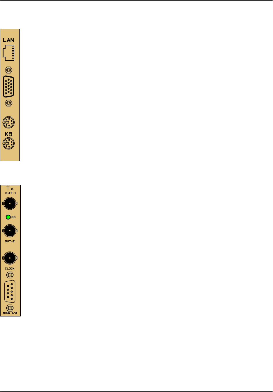
The Tx card has a BNC output for the IF Tx waveform. In addition, there is a second
output for an auxiliary signal or clock, or for a clock input. At the bottom of the card
is a 9–pin connector for arbitrary I/O (e.g., TTL, RS422, additional clock).
The RVP8 digital transmitter finds a place within the overall radar system that exactly
complements the digital receiver. The receiver samples an IF waveform that has been
down–converted from RF, and the transmitter synthesizes an IF waveform for up–con-
version to RF. The beauty of this approach is that the RVP8 now has complete control
over both halves of the radar, making possible a whole new realm of matched Tx/Rx
processing algorithms. Some examples are given below:
Phase Modulation- Some radar processing algorithms rely on modulating the phase of
the transmitter from pulse to pulse. This is traditionally done using an external IF phase
modulator that is operated by digital control lines. While this usually works well, it
requires additional hardware and cabling within the radar cabinet, and the

Introduction and Specifications
RVP8 User’s Manual
May 2003
1–14
phase/amplitude characteristics may not be precise or repeatable. In contrast, the
RVP8/Tx can perform precise phase modulation to any desired angle, without requiring
the use of external phase shifting hardware.
Pulse Compression- There is increasing demand for siting radars in urban areas
that also happen to have strict regulations on transmit emissions. Often the peak
transmit power is limited in these areas; so the job for the weather radar is to
somehow illuminate its targets using longer pulses at lower power. The problem,
of course, is that a simple long pulse lacks the ability (bandwidth) to discern
targets in range. The remedy is to increase the Tx bandwidth by modulating the
overall pulse envelope, so that a reasonable range resolution is restored. The
exceptional fidelity of the RVP8/Tx waveform can accomplish this without
introducing any of the spurious modulation components that often occur when
external phase modulation hardware is used.
Frequency Agility- This has been well studied within the research community,
but has remained out of the reach of practical weather radars. The RVP8/Tx
changes all of this, because frequency agility is as simple as changing the center
frequency of the synthesized IF waveform. Many new Range/Doppler unfolding
algorithms become possible when multiple transmit frequencies can coexist.
Frequency agility can also be combined with pulse compression to remedy the
blind spot at close ranges while the long pulse is being transmitted.
COHO synthesis- The RVP8/Tx output waveform can be programmed to be a
simple CW sine wave. It can be synthesized at any desired frequency and
amplitude, and its phase is locked to the other system clocks. If you need a
dedicated oscillator at some random frequency in the IF band, this is a simple
way to get it.
Introduction and Specifications
RVP8 User’s Manual
May 2003
1–15
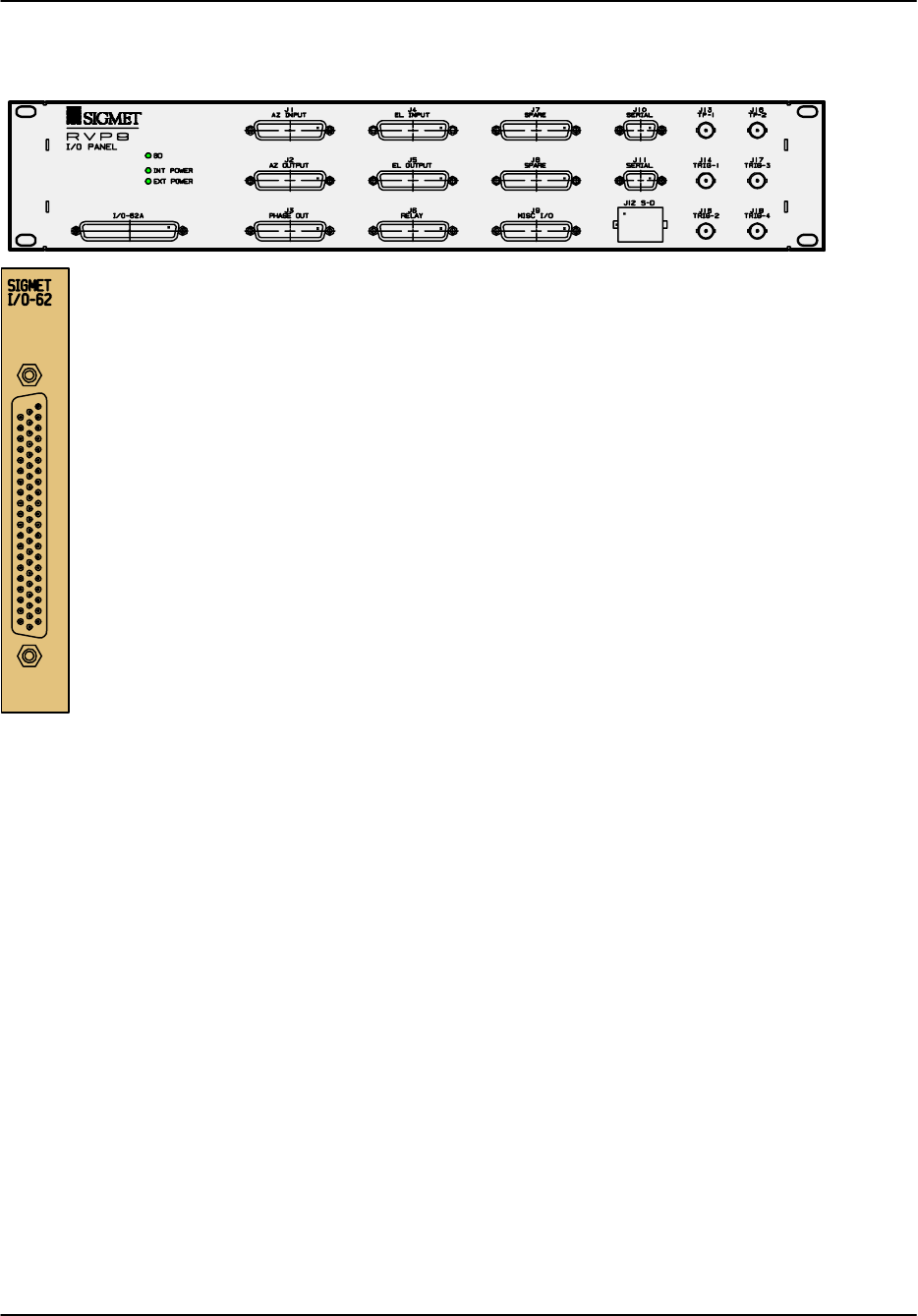
1.1.5 I/O-62 PCI Card and I/O Panel
The SIGMET I/O-62 is a short format PCI card that provides extensive I/O capabilities
for the RVP8. A typical installation would have one I/O-62 and an RVP8 Connector
Panel shown above. The Softplane is used to interconnect the I/O 62 with other SIG-
MET PCI cards. Note that the identical card is used in the SIGMET RCP8 radar/anten-
na control processor which in general does not use the Softplane connection. The
I/O-62 has a single 62-position, high-density “D” connector. This is attached to the
RVP8 Connector Panel (typically mounted on the front or back of the rack which holds
the RVP8). A standard 1:1 cable connects the remote panel to the I/O-62 card in the
RCP8 chassis. The standard connector panel provided by SIGMET meets the needs of
most radar sites.
The best part is that the I/O-62 is configurable in software, i.e., there is no need to open
the chassis to configure jumpers or switches. This means that when a spare board is
added, there is no need to perform hardware configuration or custom wiring.
The physical I/O lines are summarized in the system specifications section.
ESD Protection Features
Since the I/O lines are connected to the radar system, there is a potential for lightning or other
ESD type damage. This is addressed aggressively by the I/O-62 in two ways:
Every wire is protected by a Tranzorb diode which transitions from an open to
a full clamp between ±27 to ±35 VDC. Additionally, the Connector Panel uses
Tranzorb diodes on every I/O line for double protection.
High-voltage tolerant front-end receivers/drivers are used. All components
connected to the external pins can tolerate up to ±40V. For example, the TTL
and wide range inputs use protectors that normally look like 100 Ohm resistors,
but open at high voltage.

Introduction and Specifications
RVP8 User’s Manual
May 2003
1–16
Run Time FPGA Configuration
The SIGMET I/O-62 card is built around a 100K–Gate FPGA which, in addition to driving the
I/O signals on the 62-position connector, also coordinates the PCI and Softplane traffic. These
chips are SRAM–based, meaning that they are configured at run time. This allows the FPGA
code to be automatically upgraded during each RVP8 code release without needing to physically
reprogram any parts.
The board’s basic I/O services use up only 40% of the complete FPGA. The leftover space
makes it possible to add smart processing right on the I/O-62 board to handle custom needs. For
example the 16–bit floating–point (I,Q) data in the previous example could be reformatted into a
32–bit fixed–point stream. Other examples include generating custom serial formats, data
debouncing, and signal transition detection. In general, I/O functions that would either be
tedious or inappropriate for the host computer SBC can likely be moved onto the I/O-62 card
itself.

Introduction and Specifications
RVP8 User’s Manual
May 2003
1–17
1.2 Comparison of Analog vs Digital Radar Receivers
1.2.1 What is a Digital IF Receiver?
A digital IF receiver accepts the analog IF signal (typically 30 MHz), processes it and outputs a
stream of wide dynamic range digital “I” and “Q” values. These quantities are then processed to
obtain the moment data (e.g., Z, V, W or polarization variables). Additionally, the digital
receiver can accept the transmit pulse “burst sample” for the purpose of measuring the
frequency, phase and power of the transmit pulse. The functions that can be performed by the
digital receiver are:
IF band pass filtering
“I” and “Q” calculation over wide dynamic range
Phase measurement and correction of transmitted pulse for magnetron systems –
from burst sample
Amplitude measurement and correction of transmitted pulse – from burst sample
Frequency measurement for AFC output – from burst sample
The digital approach replaces virtually all of the traditional IF receiver components with flexible
software-controlled modules that can be easily adapted to function for a wide variety of radars
and operational requirements.
The digital receiver approach made a very rapid entry into the weather radar market. Up until
the about 1997 weather radars were not supplied with digital receivers. Today in 2003 nearly all
new weather radars and weather radar upgrades use the digital receiver approach. Much of this
rapid change is attributed to the previous generation RVP7 which is the most widely sold
weather radar signal processor of all time.
The number one advantage of a digital receiver is that it achieves a wide linear dynamic range
(e.g., >95dB depending on pulse width) without having to use AGC circuits which are complex
to build, calibrate and maintain. However, there are other advantages as well:
Lower initial cost by eliminating virtually all IF receiver components.
Lower life cycle cost do to reduced maintenance.
Selectable IF frequency.
Software controlled AFC with automatic alignment.
Programmable band pass filter
Dual or multiple IF multiplexing
Improved remote monitoring down to the IF level.
The following sections compare the digital receiver approach to the analog receiver approach.
This illustrates the advantages of the digital approach and what functions are performed by a
digital receiver.

Introduction and Specifications
RVP8 User’s Manual
May 2003
1–18
1.2.2 Magnetron Receiver Example
A typical analog receiver for a magnetron system is shown in the top portion of Figure 1–1. The
received RF signal from the LNA is first mixed with the STALO (RF–IF) and the resulting IF
signal is applied to one of several bandpass filters that match the width of the transmitted pulse.
The filter selection is usually done with relays. The narrow band waveform is then split. Half is
applied to a LOG amplifier having a dynamic range of 80–100dB, from which a calibrated
measurement of signal power can be obtained. The LOG amplifier is required because it is
almost impossible to build a linear amplifier with the required dynamic range. However, phase
distortion within the LOG amplifier renders it unsuitable for making Doppler measurements;
hence, a separate linear channel is still required.
The linear amplifier is fed from the other half of the bandpass filter split. It may be preceded by
a gain control circuit (IAGC) which adjusts the instantaneous signal strength to fall within the
limited dynamic range of the linear amplifier. The amplitude and phase characteristics of the
IAGC attenuator must be calibrated so that the “I” and “Q” samples may be corrected during
processing.
The IF output from the linear amplifier is applied to a pair of mixers that produce “I” and “Q”.
The mixer pair must have very symmetric phase and gain characteristics, and each must be
supplied with an accurate 0-degree and 90-degree version of the Coherent Local Oscillator
(COHO). The later is usually obtained by sampling a portion of the transmitted pulse, and then
phase locking an oscillator (COHO) that continues to “ring” afterward. Phase locked COHO’s
of this sort can be very troublesome – they often fail to lock properly, drift with age, and fail to
maintain coherence over the full unambiguous range.
The transmit burst that locks the COHO is also used by the Automatic Frequency Control (AFC)
loop. The AFC relies on an FM discriminator and low pass filter to produce a correction voltage
that maintains a constant difference between the magnetron frequency and the reference STALO
frequency. The AFC circuit is often troublesome to set and maintain. Also, since it operates
continuously, small phase errors are continually being introduced within each coherent
processing interval.
In contrast, the RVP8 digital receiver is shown in to lower portion of Figure 1–1. The only old
parts that still remain are the microwave STALO oscillator, and the mixer that produces the
transmit burst. The burst pulse and the analog IF waveform are cabled directly into the IFD on
SMA coax cables. Likewise, the AFC control voltage is also a simple direct connection either
with analog tuning (+–10V from IFD) or digital control via the optional DAFC interface. These
cables constitute the complete interface to the radar’s internal signals; no other connections are
required within the receiver cabinet.
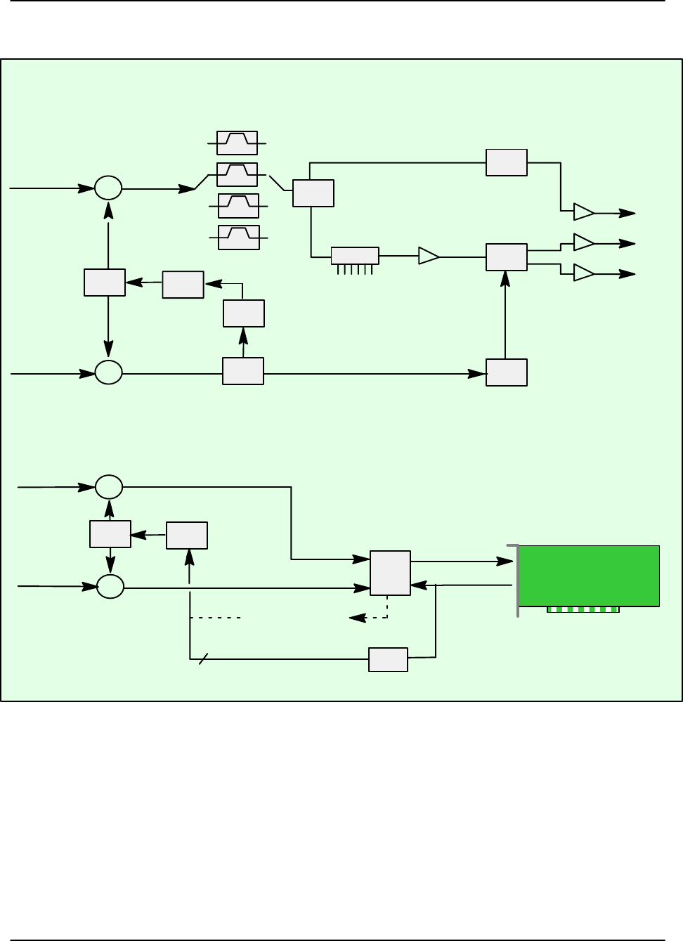
Introduction and Specifications
RVP8 User’s Manual
May 2003
1–19
Figure 1–1: Analog vs Digital Receiver for Magnetron Systems
Classic Analog Receiver for Magnetron
Analog IF
IF
Digital Atten
Control Bits
IAGC
Split
LOG
Linear Amp
Quad Phase
Detector
COHO
RVP8 Magnetron Interface
Analog IF
From IAGC Logic
IF
Digitizer Fiber Optic
RF Tx Burst
Split
XSplit
AFC
IF Tx Sample
IF Tx Sample
X
Digital AFC Control
COAX
Uplink
AFC Signal
I
Q
LOG
Line Drivers
Low Q Locking COHO
IF Filters Matched to
Pulse Widths
BPF
BPF
BPF
IFD
Downlink
DAFC
+–10V Analog AFC
X
X
Analog RF
From LNA
BPF
Analog RF
From LNA
Split
24 bits
Phase
Locked
RVP8/Rx
Optional
STALO
RF Tx Burst
STALO
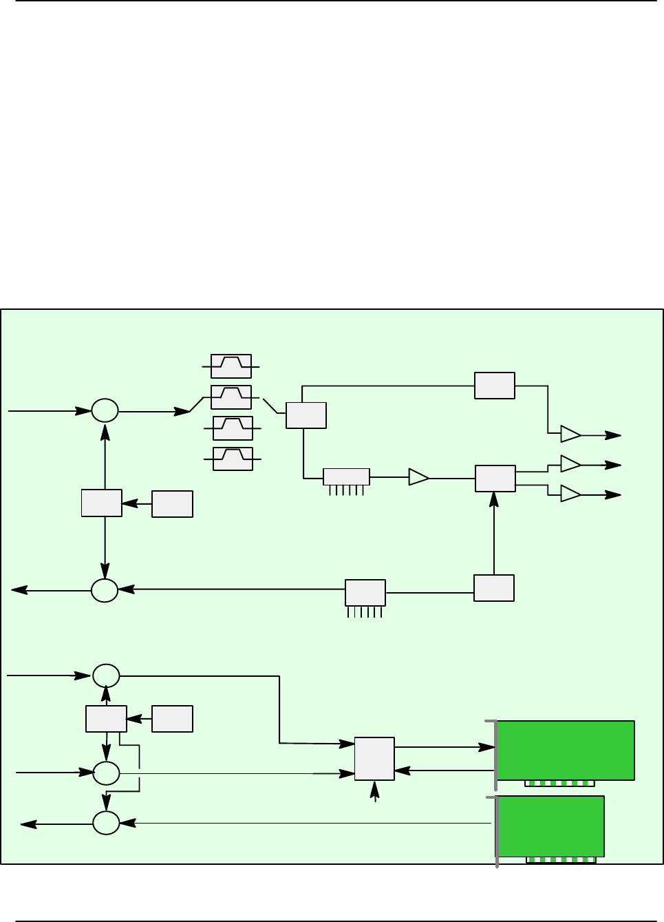
Introduction and Specifications
RVP8 User’s Manual
May 2003
1–20
1.2.3 Klystron or TWT Receiver and Transmit RF Example
A typical analog receiver for a klystron system is shown in the top portion of Figure 1–2. The
arrangement of components is similar to the magnetron case, except that the COHO operates at a
fixed phase and frequency, a phase shifter is included for 2nd trip echo filtering and there is no
AFC feedback required. The phase stability of a Klystron system is better than a magnetron, but
the system is still constrained by limited linear dynamic range, IAGC inaccuracy, quad phase
detector asymmetries, phase shifter inaccuracies, etc.
The RVP8/Tx card now plays the role of a programmable COHO. The digitally synthesized
transmit waveform can be phase, frequency and amplitude modulated (no separate phase shifter
is required) and even produce multiple simultaneous transmit frequencies. These capabilities are
used to support advanced algorithms, e.g., range/velocity ambiguity resolution or pulse
compression for low power TWT systems.
Figure 1–2: Analog vs Digital Receiver for Klystron Systems
Classic Receiver and Transmit RF for Klystron
COHO
RVP8 Klystron Interface
Transmit RF
X
To Klystron
Analog IF
IF
Digital Atten
Control Bits
IAGC
Split
LOG
Linear Amp
Quad Phase
Detector
From IAGC Logic
Split
I
Q
LOG
Line Drivers
BPF
BPF
BPF
X
Analog RF
From LNA
BPF
Analog IF
IF
Digitizer Fiber Optic
IF Tx Sample
RF Tx Sample
X
Digital Synthesized IF (smart COHO)
COAX
Uplink
IFD
Downlink
X
Analog RF
From LNA
Split
X
Transmit RF
To Klystron
Optional CLK
RVP8/Tx
RVP8/Rx
∆φ
Phase Shifter
Control Bits
STALO
STALO

Introduction and Specifications
RVP8 User’s Manual
May 2003
1–21
1.3 RVP8 IF Signal Processing
1.3.1 IFD Data Capture and Timing
The RVP8 design concept is to perform very little signal processing within the IFD digitizer
module itself. This is to minimize the presence of digital components that might interfere with
the clean capture of the IF signals.
The digitized IF and burst pulse samples are multiplexed onto the fiber channel link which
provides the digital data to the RVP8/Main board at approximately 540-MBits/sec. The 14-bit
samples are encoded for transmission over a fiber channel link. This optical link allows the IFD
to be as far as 100 meters away from the RVP8/Main board and provides an added degree of
noise immunity and isolation.
The uplink input from the RVP8/Main board provides the timing for multiplexing the burst pulse
sample with the IF signal. In addition, it is used to set the AFC DAC or digital output level, and
to perform self tests.
The sample clock oscillator in the IFD is selected to be very stable. The sample clock serves a
similar function to the COHO on a traditional Klystron system, i.e., it is the master time keeper.
Because of this the IFD sample clock is used to phase lock the entire RVP8, i.e., the Rx, Tx,
IO-62 boards and the SoftPlane are all phase locked to the IFD sample clock. Designers have
two choices for factory configuration of the IFD sample clock:
A fixed crystal frequency selected to achieve a desired range resolution. The
standard range resolution corresponds to 25 m increments.
A very narrow band VCXO (50 ppm) selected to lock to an input reference signal
from the radar, and provide a desired range resolution. SIGMET stocks VCXO’s
for 25 m range resolution increments for reference inputs of 10, 20, 30 and 60
MHz. Custom frequency VCXO’s are available on request. Examples of external
reference signal sources are an external COHO, external STALO reference or
perhaps even a GPS clock).
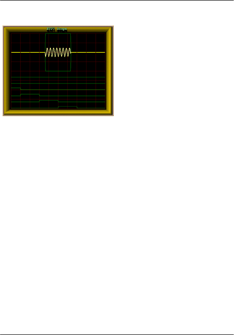
Introduction and Specifications
RVP8 User’s Manual
May 2003
1–22
1.3.2 Burst Pulse Analysis for Amplitude/Frequency/Phase
The burst pulse analysis provides the ampli-
tude, frequency and phase of the transmitted
pulse. The phase measurement is analogous to
the COHO locking that is performed by a tradi-
tional magnetron radar. The difference is that
the phase is known in the digital technique, so
that range dealiasing using the phase modula-
tion techniques is possible. Amplitude mea-
surement (not performed by traditional radars)
can provide enhanced performance by allow-
ing the “I” and “Q” values to be corrected for
variations in the both the average and the pulse-
to-pulse transmitted power. In addition, a
warning is issued if the burst pulse amplitude
falls below a threshold value.
The burst pulse data stream is first analyzed by an adaptive algorithm to locate the burst pulse
power envelope (e.g. 0.8 sec). The algorithm first does a coarse search for the burst pulse in the
time/frequency domain (by scanning the AFC) and then does a fine search in both time and
frequency, to assure that the burst is centered at “range 0” and is at the required IF value. The
power-weighted phase of the burst pulse and the total burst pulse power is then computed. The
power weighted average phase is used to make the digital phase correction. Phase jitter for
magnetron systems with good quality modulator and STALO is better than 0.5 degrees RMS, as
measured on actual nearby clutter targets. For Klystron systems, the phase locking is better than
0.1 degree RMS.
The burst pulse frequency is also analyzed to calculate the frequency error from the nominal IF
frequency. For magnetron systems, the error is filtered with a selectable time constant which is
typically set to several minutes to compensate for slow drift of the magnetron. The digital
frequency error is sent via the uplink to the IFD in the receiver cabinet where a DAC converts it
into an analog output to the magnetron STALO. Optionally, a DAFC unit can be Teed off the
uplink cable to interface to Klystron systems do not require the AFC.
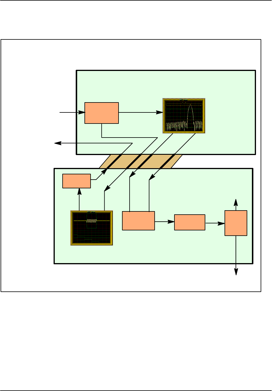
Introduction and Specifications
RVP8 User’s Manual
May 2003
1–23
1.3.3 Rx Board and CPU IF to I/Q Processing
Figure 1–3: IF to I/Q Processing Steps
Fiber Optic
Receiver
Digital IF
IF Tx Samples
Bandpass Filter
Digital Quad Phase
and
Decompression
Tx Burst Pulse
Analysis
Frequency
Amplitude/
Phase
Correction
Interference
Filter
AFC
Servo
I/Q
Signal I/Q Tx
Burst
IFD Fiber Optic
Downlink
IFD COAX
Uplink
Digitized IF Signal
and Tx Burst Sample
Timing and digital AFC
IF to I/Q Processing Steps
1000 BaseT
Ethernet
UDP Broadcast I/Q
Samples to recording
system or separate
processing system
Digital FIR
RVP8/Rx
CPU
PCI
I/Q
Digital AFC
I/Q Moment
Processing
IF Tx
Samples
I/Q
Tx Burst
I/Q
Signal
I/Q Time
Series
API
The RVP8/Rx board performs the initial processing of the IF digital data stream and outputs “I”
and “Q” data values to the host computer via the PCI bus. In addition, the frequency, phase and
amplitude of the burst pulse are measured. The functions performed by the processor are:
Reception of the digital serial fiber optic data stream.
Band pass filtering of the IF signal using configurable digital FIR filter matched
to the pulsewidth.
Range gating and optional coherent averaging (essentially performed during the
band pass filtering step).
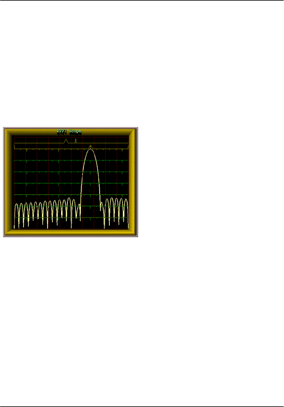
Introduction and Specifications
RVP8 User’s Manual
May 2003
1–24
Computation of “I” and “Q” quadrature values (also performed during the band
pass filtering step).
Transmit burst sample frequency, phase and amplitude calculation
I and Q phase and amplitude correction based on transmit burst sample.
Interference rejection algorithm.
AFC frequency error calculation with output to IFD for digital or analog control
of STALO (for magnetron systems).
The advantage of the digital approach is that the software algorithms for these functions can be
easily changed. Configuration information (e.g., processor major mode, PRF, pulsewidth, gate
spacing, etc.) is supplied from the host computer.
The digital matched filter that computes “I”
and “Q” is designed in an interactive man-
ner using a TTY and oscilloscope for graph-
ical display. The filter’s passband width
and impulse response length are chosen by
the user, and the RVP8 constructs the filter
coefficients using built-in design software.
The frequency response of the filter can be
displayed and compared to the frequency
content of the actual transmitted pulse.
Microwave energy can come from a variety of transmitters such as ground-based, ship-based or
airborne radars as well as communications links. These can cause substantial interference to a
weather radar system. Interference rejection is provided as standard in the RVP8. Three different
interference rejection algorithms are supported.
The RVP8/Rx board places the wide dynamic range “I” and “Q” samples directly on the PCI
bus where they are sent to the processor section of the PC (e.g., dual Pentium processors on a
single-board computer or motherboard). The I/Q values are then processed on the Pentium
processors to extract the moment information (Z, V, W and optional polarization parameters).
The I and Q values can also be placed on a gigabit Ethernet line (1000 BaseT) which is provided
directly on the processor board. This means that there is no second PCI bus “hit” required to
send the data to a recording system or a completely separate processing system.

Introduction and Specifications
RVP8 User’s Manual
May 2003
1–25
1.4 RVP8 Weather Signal Processing
The processing of weather signals by the RVP8 is based on the algorithms used in the previous
generation RVP7 and RVP6. However, the performance of the RVP8 allows a different approach
to some of the processing algorithms, especially the frequency domain spectrum processing. All
of the algorithms start with the wide dynamic range I and Q samples that are obtained from the
Rx card over the PCI bus.
The resulting intensity, radial velocity, spectrum width and polarization measurements are then
sent to a separate host computer to serve as input for applications such as:
Quantitative Rainfall Measurement
Vertical Wind Profiling
ZDR Hail Detection
Tornado Detection and Microburst Detection
Gust Front Detection
Particle Identification
Target Detection and Tracking
General Weather Monitoring
To obtain the basic moments, the RVP8 offers the option of several major processing modes:
Pulse Pair Mode Time Domain Processing
DFT/FFT Mode Frequency Domain Processing
Random Phase Mode for 2nd trip echo filtering
Polarization Mode Processing
Note that the RVP8 is the first commercial processor to perform discrete Fourier transforms
(DFT) as well as fast Fourier transforms (FFT). FFT is more computationally efficient than
DFT, but the sample size is limited to be a power of two (16, 32, 64, ...) This is too restrictive on
the scan strategy for a modern Doppler radar since this means, for example, that a one degree
azimuth radial must be constructed from say exactly 64 input I/Q values. The RVP8 has the
processing power such that when the sample size is not a power of 2, a DFT is performed instead
of an FFT
These modes share some common features that are described first, followed by descriptions of
the unique features of each mode.
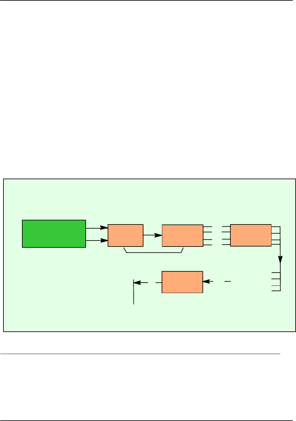
Introduction and Specifications
RVP8 User’s Manual
May 2003
1–26
1.4.1 General Processing features
Figure 1–4 shows a block diagram of the processing steps. These are discussed below.
Autocorrelations
The autocorrelations R0, R1 and R2 are produced by all three processing modes. However, the
way that they are produced is different for the three modes, particularly with regard to the
filtering that is performed.
Pulse Pair Mode– Filtering for clutter is performed in the time domain.
Autocorrelations are computed in the time domain.
DFT/FFT Mode– Filtering for clutter is performed in the frequency domain by an
adaptive algorithm. Autocorrelations are computed from the inverse transform.
Random Phase– Filtering for clutter and second trip echo is performed in the
frequency domain by adaptive algorithms. Autocorrelations are computed from
the inverse transform.
Figure 1–4: I/Q Processing for Weather Moment Extraction
Moment and
Threshold
Calculations
Clutter Filter
I
Q
Autocorrelations
RVP8 Standard Moment Processing Steps
Clutter Micro
Suppression and
Range Averaging
Thresholding
Speckle Filter
T
Z
V
W
SQI
LOG
SIG
CCOR
T0
R0
R1
R2
T0
R0
R1
R2
T
Z
V
W
Pulse Pair, FFT/DFT, Random Phase Modes
10/100/1000 BaseT
Ethernet
To Applications Host Computer
Time Series
API
The use of the R2 lag provides improved estimation of signal-to-noise ratio and spectrum width.
Processors that do not use R2 cannot effectively measure the SNR and spectrum width.

Introduction and Specifications
RVP8 User’s Manual
May 2003
1–27
Time (azimuth) Averaging
The autocorrelations are based on input “I” and “Q” values over a selectable number of pulses
between 8, 9, 10, ...,256. Any integer number of pulses in this interval may be used including
DFT/FFT and random phase modes.
Selectable angle synchronization using the input AZ and EL tag lines assures that all possible
pulses are used during averaging for each, say, 1 degree interval. This minimizes the number of
“wasted” pulses for maximum sensitivity. Azimuth angle synchronization also assures the
accurate vertical alignment of radial data from different elevation angles in a volume scan (see
below).
TAG Angle Samples of Azimuth and Elevation
During data acquisition and processing it is usually necessary to associate each output ray with
an antenna position. To make this task simpler the RVP8 samples 32 digital input “TAG” lines,
once at the beginning and once at the end of each data acquisition period. These samples are
output in a four-word header of each processed ray. When connected to antenna azimuth and
elevation, the TAG samples provide starting and ending angles for the ray, from which the
midpoint could easily be deduced. Since the bits are merely passed on to the user, any angle
coding scheme may be used. The processor also supports an angle synchronization mode, in
which data rays are automatically aligned with a user-defined table of positions. For that
application, angles may be input either in binary or BCD.
Range Averaging and Clutter Microsuppression
To improve the accuracy of the reflectivity measurements, the RVP8 can perform range
averaging. When this is done, autocorrelations from consecutive range bins are averaged, and
the result is treated as if it were a single bin. This type of averaging is useful to lower the
number of range bins that the host computer must process.
Range averaging of the autocorrelations may be performed over 2, 3, 4, ..., 16 bins. Prior to
range averaging, any bins that exceed the selectable clutter-to-signal threshold are discarded.
This prevents isolated strong clutter targets from corrupting the range average, which improves
the sub-clutter visibility.
Moment Extraction
The autocorrelations serve as the basis for the Doppler moment calculations,
Mean velocity – from Arg [ R1 ]
Spectrum width – from |R1| and |R2| assuming Gaussian spectrum
dBZ – from R0 with correction for ground clutter, system noise and gaseous
attenuation. Uses calibration information supplied by host computer.
dBT – identical to dBZ except without ground clutter.
These are the standard parameters that are output to the host computer on the high-speed
Ethernet interface.

Introduction and Specifications
RVP8 User’s Manual
May 2003
1–28
Thresholding
The RVP8 calculates several parameters that are used to threshold (discard) bins with weak or
corrupted signals. The thresholding parameters are:
Signal quality index (SQI=|R1|/R0)
LOG (or incoherent) signal-to-noise ratio (LOG)
SIG (coherent) signal-to-noise ratio
CCOR clutter correction
These parameters are computed for each range bin and can be applied in AND/OR logical
expressions independently for dBZ, V and W.
Speckle Filter
The speckle filter can be selected to remove isolated single bins of either velocity/width or
intensity. This feature eliminates single pixel speckles which allows the thresholds to be reduced
for greater sensitivity with fewer false alarms (speckles). Both a 1D (single azimuth ray) and 2D
(3 azimuth rays by 3 range bins) are supported.
Velocity Unfolding
A special feature of the RVP8 processor is its ability to “unfold” mean velocity measurements
based on a dual PRF algorithm. In this technique two different radar PRF’s are used for
alternate N-pulse processing intervals. The internal trigger generator automatically produces the
correct dual-PRF trigger, but an external trigger can also be applied. In the later case, the
ENDRAY_ output line provides the indication of when to switch rates. The RVP8 measures the
PRF to determine which rate (high or low) was present on a given processing interval, and then
unfolds based on either a 2:3, 3:4 or 4:5 frequency ratio. Table 1–1 gives typical unambiguous
velocity intervals for a variety of radar wavelengths and PRF’s.
Table 1–1: Examples of Dual PRF Velocity Unfolding
Unambiguous Velocity (m/s) for
Various Radar Wavelengths
PRF1 PRF2 Unambiguous
Range (km) 3 cm 5 cm 10 cm
500 * 300 3.75 6.25 12.50 No
U f ldi
1000 * 150 7.50 12.50 25.00 Unfolding
2000 * 75 15.00 25.00 50.00
500 333 300 7.50 12.50 25.00 Two
Ti
1000 667 150 15.00 25.00 50.00 Times
Unfolding
2000 1333 75 30.00 50.00 100.00
Unfolding

Introduction and Specifications
RVP8 User’s Manual
May 2003
1–29
PRF1 10 cm5 cm3 cm
Unambiguous
Range (km)
PRF2
500 375 300 11.25 18.75 37.50 Three Times
U f ldi
1000 750 150 22.50 37.50 75.00 Unfolding
2000 1500 75 45.00 75.00 150.00
500 400 300 15.00 25.00 50.00 Four
Ti
1000 800 150 30.00 15.00 100.00 Times
Unfolding
2000 1600 75 60.00 100.00 200.00
Unfolding
1.4.2 RVP8 Pulse Pair Time Domain Processing
Pulse pair processing is done by direct calculation of the autocorrelation. Prior to pulse pair
processing, the input “I” and “Q” values are filtered for clutter using a a time domain notch
filter. Filters of various selectable widths are available for either 40 or 50 dB stop band
attenuation. The filtered I/Q values are processed to obtain the autocorrelation lags R0, R1 and
R2. The unfiltered power is also calculated (T0). The autocorrelations are then sent to the range
averaging and moment extraction steps.
1.4.3 RVP8 DFT/FFT Processing
The DFT/FFT mode allows clutter cancelation to be performed in the frequency domain. DFT is
used in general, with FFT’s used if the requested sample size is a power of 2.
Three standard windows are supported to provide the best match of window width to the
spectrum dynamic range:
Rectangular
Hamming
Blackman
After the FFT step, clutter cancelation is done using a selectable fixed width filter that
interpolates across the noise or any overlapped weather or an adaptive filter which automatically
determines the optimal width. This technique preserves overlapped weather as compared to time
domain notch filters which will always attenuate overlapped weather to some extent, depending
on the spectrum width. After clutter cancelation, R0, R1 and R2 are computed by inverse
transform and these are used for moment estimation.

Introduction and Specifications
RVP8 User’s Manual
May 2003
1–30
1.4.4 Random Phase Processing for 2nd Trip Echo
Second trip echoes can be a serious problem for applications that require operation at a high
PRF. Second trip echoes can appear separately or can be overlaid on first trip echoes (second trip
obscuration). The random phase technique separates the first and second trip echoes so that:
In nearly all cases, the 2nd trip echo can be removed from the first trip even in the
case of overlapped 1st and 2nd trip echoes. The benefit is a clean first trip display.
The 2nd trip echoes can be recovered and placed at their proper range at 1st
trip/2nd trip signal ratios of up to 40 dB difference for overlapped echoes.
Because of the wide dynamic range of weather echoes, this power limit will
sometimes be exceeded.
The technique requires that the phase of each pulse be random. Digital phase correction is then
applied in the processor for the first and second trips. The critical step is the adaptive filter
which removes the echo of the other trip to increase the SNR. Magnetrons have a naturally
random phase. For Klystron radars, a digitally controlled precision IF phase shifter is required.
The RVP8 provides an 8-bit RS422 output for the phase shifter.
For more information on the technique refer to Joe, et. al., 1995.
1.4.5 Polarization Mode Processing
Polarization processing uses a time domain autocorrelation approach to calculate the various
parameters of the polarization co-variance matrix, i.e., ZDR, LDR, PHIDP, RHOHV, PHIDP
(KDP), etc. In addition, the standard moments T, V, Z, W are also calculated. Which parameters
are available and which algorithms are used to calculate them depends on the type of
polarization radar, e.g., single channel switching, simultaneous transmit and receive (STAR),
dual channel switching. SIGMET, Inc. is licensed by US National Severe Storms Laboratory
(NSSL) to use the STAR hardware and processing techniques and algorithms.
Polarization measurements require special calibration of the ZDR and LDR offsets. The use of a
clutter filter for the polarization variables can sometimes bias the derived parameters. Because of
this, the user decides whether or not to use filtered or unfiltered time series.
1.4.6 Output Data
The RVP8 output data for standard moment calculations consist of mean radial velocity (V),
Spectrum Width (W), Corrected Reflectivity(Z or dBZ) and Uncorrected Reflectivity (T or
dBT). Other data outputs include I/Q time series, DFT/FFT power spectrum points and
polarization parameters. The output can be made in either 8 or 16-bit format. 8-bit format is
preferred over 16-bit format for most applications since the accuracy is more than adequate for
an operational radar system, and the data communications are reduced by 50%. 16-bit formats
are sometimes used by research customers for data archive purposes. Note that time series and
FFT are always 16-bit formats. All data formats are documented in Chapter 6 of this manual.
A standard output is the I/Q time series on gigabit network (1000 BaseT). These are sent via
UDP broadcast to an I/Q archiving system or even a completely independent parallel processing
system.

Introduction and Specifications
RVP8 User’s Manual
May 2003
1–31
1.5 RVP8 Control and Maintenance Features
1.5.1 Radar Control Functions
The RVP8 also performs several important radar control functions:
Trigger generation- up to 6 programmable triggers.
Pulsewidth control (four states controlled by four bits).
Angle/data synchronization- to collect data at precise azimuth intervals (e.g.,
every 0.5, 1, 1.5 degrees) based on the AZ/EL angle inputs.
Phase shifter- to control the phase on legacy Klystron systems. New or upgrade
Klystron or TWT systems can use the RVP8/Tx card to provide very accurate
phase shifting.
ZDR switch control- for horizontal/vertical or other polarization switching
scheme.
AFC output (digital or analog) based on the burst pulse analysis for magnetron
systems.
Pulsewidth and trigger control are both built into the RVP8. Four TTL output lines can be
programmed to drive external relays that control the transmitter pulsewidth. The internal trigger
generator drives six separate lines, each of which can be programmed to produce a desired
waveform. The trigger generator is unique in that the waveforms are stored in RAM and can be
modified interactively by user software. Thus, precisely delayed and jitter-free strobes and gates
can easily be produced. For each pulsewidth there is a corresponding maximum trigger rate that
can be generated. Note, however, that the RVP8 can also operate from an external user-supplied
trigger. In either case, the processor measures the trigger period between pulses so that user
software can monitor it as needed.
The RVP8 also supports trigger blanking during which one or more (selectable) of the transmit
triggers can be inhibited. Trigger blanking is used to avoid interference with other electronic
equipment and to protect nearby personnel from radiation hazard. There are two techniques for
this:
2D AZ/EL sector blanking areas can be defined in the RVP8 itself.
An external trigger blanking signal (switch closure to ground, TTL or RS422) can
be supplied, for example from a proximity switch that triggers when the antenna
goes below a safe elevation angle or connected to the radome access hatch.

Introduction and Specifications
RVP8 User’s Manual
May 2003
1–32
1.5.2 Power-Up Setup Configuration
The RVP8 stores on disk an extensive set of configuration information. The purpose of these
data is to define the exact configuration of the RVP8 upon startup. The setup information can be
accessed and modified using either a local keyboard and monitor, or over the network. For
multiple radar networks, the configuration management can be centrally administered by
copying tested “master” configuration files to the various network radars. It is not necessary to
go to the radar to change ROM’s as was the case for previous generation processors.
1.5.3 Built-In Diagnostics
On power-up, the RVP8 performs a sequence of internal self-tests. The test sequence requires
about four seconds to perform, and tests approximately 95% of the internal digital circuitry.
Errors are isolated to specific sections of the board as much as possible. If any check fails, the
user can be certain that some component is not functioning correctly. However, there is a very
small chance that even a defective board may pass all the tests; the failure may be in one of the
few areas that can not be checked.
The RVP8 displays the test results on the LED front panel (for a standard SIGMET chassis). In
this way, there is immediate visual confirmation of the diagnostic tests, even if the host computer
has not yet been connected. The local keyboard and monitor or a networked workstation can be
used to see the test results in the TTY menus or even invoke a power–up reset and test.

Introduction and Specifications
RVP8 User’s Manual
May 2003
1–33
1.6 Support Utilities and Available Application Software
The RVP8 system includes a complete set of tools for the calibration, alignment and
configuration of the RVP8. These includes the following utilities:
ascope- a comprehensive utility for manual signal processor control and data
display of moments, times series and Doppler spectra. ascope includes a realistic
signal simulator capable of producing both first and second trip targets.
Recording/playback of time series and moments is included as well.
dspx- an ASCII text-based program to access and control the signal processor,
including providing access to the local setup menus.
speed- a performance measuring utility.
DspExport- exports the RVP8 to another workstation over the network. This
allows utilities on a remote network to run locally, as opposed to exporting the
utility display window over the network.
setup- interactive GUI for creating/editing the RVP8 configuration files.
zauto- calibration utility for use with a test signal generator.
These tools can be run locally on the RVP8 itself or over the network from a central maintenance
facility. The DspExport utility improves the performance of the utilities for network applications
by letting them be run on the workstation that is remote from the RVP8. Note that standard
X–Window export is of course supported but requires more bandwidth.
In addition, complete radar application software can be purchased from SIGMET:
IRIS/Radar on a separate PC, interfaces to the RVP8 by 100 BaseT Ethernet.
IRIS/Radar controls both the RVP8 and the SIGMET RCP8 radar/antenna control
processor. The package provides complete local and remote control/monitoring,
data processing and communication for a radar system.
IRIS/Analysis (and options) runs on a separate PC, often at a central site. One
IRIS/Analysis can support up to 20 radar systems. This functions as a radar
product generator (RPG) to provide outputs such as CAPPI, rain accumulations,
echo tops, automatic warning and tracking, etc. Optional software packages are
provided for special applications: wind shear and microburst detection,
hydrometeorology with raingage calibration and subcatchments, composite, dual
Doppler and 3D Display.
IRIS/Web provides IRIS displays to network users on standard PC’s (Windows
or Linux) running Netscape or Internet Explorer.
IRIS/Display can display products sent to it and, with password authorization,
can serve as a remote control and monitoring site for networked radar systems.
Features such as looping, cross–section, track, local warning, annotation, etc. are
all provided by IRIS/Display. Note that both IRIS/Analysis and IRIS/Radar have
all of the capabilities of IRIS/Display in addition to their own functions. This
means that any IRIS system can display products.

Introduction and Specifications
RVP8 User’s Manual
May 2003
1–34
1.7 Open Architecture and Published API
The RVP8 is largely software compatible with the RVP7, and uses the same published API
opcode interface that has evolved over the years from the RVP5, RVP6, and RVP7 products.
Driver code that has been written for the RVP7 can be easily adapted to the RVP8. The 16–bit
I/O command protocols are identical, and the data formats are unchanged. What is different is
that the RVP8 supports an Ethernet interface rather than only a SCSI interface. SIGMET
provides a free source code example for the driver in C.
In addition to assuring backward compatibility, SIGMET also recognizes that certain users may
require the ability to write their own signal processing algorithms which will run on the RVP8.
To accommodate this, the RVP8 software is organized to allow separately compiled plug-in
modules to be statically linked into the running code. The application program interface (API)
allows user code to be inserted at the following stages of processing:
Tx/Rx waveform synthesis and matched filter generation— The API allows the
transmit waveforms to be defined from pulse to pulse, along with the
corresponding FIR coefficients that will extract (I,Q) from that Tx waveform.
This allows users to experiment with arbitrary waveforms for pulse compression
and frequency agility.
Time series and spectra processing from (I,Q)- The API allows you to modify the
default time series and spectra data, e.g., to perform averaging or windowing in a
different way.
Parameter generation from (I,Q)- This is probably where the greatest activity will
occur for user–supplied code. The API allows you to redefine how the standard
parameters (dBZ, Velocity, Width, PHIDP, etc.) are computed from the incoming
(I,Q) time series. You may also create brand new parameter types that are not
included in the basic RVP8 data set.
Note that the standard SIGMET algorithms are not made public in this model. Rather, the
interface hooks and development tools are provided so that users can add their own software
extensions to the RVP8 framework. Many of the library routines that are fundamental to the
RVP8 are also documented and can be called by user code; but the source to these routines is not
generally released. Development tools which are not under public license must be purchased
separately by the customer.
While most customers will use the signal processing software supplied by SIGMET, the new
open software architecture approach employed by the RVP8 will be very useful to those research
customers who want to try innovative new approaches to signal processing, or to those OEM
manufacturers who are interested in having their own “custom” stamp on the product.

Introduction and Specifications
RVP8 User’s Manual
May 2003
1–35
1.8 RVP8 Technical Specifications
1.8.1 IFD Digitizer Module
Input Signals
IF Received Signal: 50, + 6.5 dBm max
IF Magnetron Burst or COHO: 50, +6.5 dBm max
Optional Reference Clock: 2–60 MHz –10 to 0 dBm
IF Ranges
6 to 16MHz, 20-34 MHz, 38-52 MHz, 56-70 MHz
Linear Dynamic Range
90 to >100dB depending on pulsewidth/bandwidth filter
A/D Conversion
Resolution 14 bit with jitter <2.5 picosec
Sampling rate 33.5 to 39.5 MHz (selectable, standard is 35.975 MHz)
AFC Output
Analog –10 to +10V
Optional Digital AFC (DAFC) with up to 24 programmable output bits.
Automatic 2-D (time/frequency) burst pulse search and fine tracking algorithms.
Fiber Optic Down Link
540 MHz optical link, 62.5/125-micron multimode ST cable.
Coax Uplink
75 electrically isolated (16K) from receiver’s ground.
Maximum Separation from RVP8/Rx
100 meters, with automatic calibration of round trip time and range correction.

Introduction and Specifications
RVP8 User’s Manual
May 2003
1–36
1.8.2 RVP8/Rx PCI Card
Pulse Repetition Frequency
50 Hz to 20 KHz +0.1%, continuously selectable.
IF Band Pass Filter
Programmable Digital FIR with software selectable bandwidth. Built-in filter
design software with graphical user interface.
Impulse Response
Up to 3024 FIR filter taps, corresponding to approximately 84 sec impulse
response length for 36 MHz IF samples. These very long filters are intended for
use with pulse compression.
Range Resolution
Minimum bin spacing of 25 meters selectable in N*8.33 meter steps. Bins can be
positioned in a configurable range mask with resolution of N* the fundamental
bin spacing, or arbitrarily to an accuracy of ±2.2 meters.
Maximum Range
Up to 1024 km
Number of Range Bins
Full unambiguous range at minimum resolution or 2048 range bins (whichever is
less).
Electrical and Optical Interfaces
Receives fiber-optic downlink from the RVP8/IFD, and generates the 75 coax
uplink to the RVP8/IFD.
BNC #1 for trigger output (12V, 75), or pretrigger input.
BNC #2 for trigger output (12V, 75).
Data Output via PCI Bus
16–bit I and Q values
14-bit raw IF samples

Introduction and Specifications
RVP8 User’s Manual
May 2003
1–37
1.8.3 RVP8/Tx PCI Card
Analog Waveform Applications
Digitally synthesized IF transmit waveform for pulse compression, frequency
agility, and phase modulation applications.
Master clock or COHO signal to the radar; can be phase locked or free running,
arbitrary frequency.
Analog Output Waveform Characteristics
Two independent, digitally synthesized, analog output waveforms (BNC). These
two outputs are electrically identical and logically independent IF waveform
synthesizers that can produce phase modulated CW signals, finite duration pulses,
compressed pulses, etc.
Can drive up to +12dBm into 50.
14-bit interpolating TxDAC provides 71dB Signal-to-Noise Ratio.
IF center frequency selectable from 8 to 32.4 MHz, and from 48.6 to 75MHz.
Signal bandwidth as large as 15MHz for wideband/multiband Tx applications.
Total harmonic distortion less than –74dB.
Waveform pre-emphasis compensates for both static and dynamic Tx
nonlinearities.
Other I/O signals
Clock In/Out 50 SMA connector. This can receive a CW reference frequency
to which the RVP8/Tx can lock to a P/Q frequency multiple (much like the
RVP8/IFD can lock to an external reference). This connector can also supply the
TxData Clock, optionally divided by some N between 1 and 16, in order to
supply external circuitry with +10dBm clock reference at 50.
9-pin “D” connector supporting four RS-422 differential signals for
miscellaneous input and output with SoftPlane support.. Each line pair can
operate as a transmitter or as a receiver depending on what’s needed. Possible
uses are: alternate reference clock input, gating input for CW modes, additional
trigger outputs, external phase shift requests, etc.

Introduction and Specifications
RVP8 User’s Manual
May 2003
1–38
1.8.4 SIGMET I/O-62 PCI Card
Short format PCI card with 62-position “D” connector. Multiple cards may be
installed.
Includes D/A, A/D, discrete inputs and outputs (TTL, wide range, RS422, etc.)
See summary table below.
I/O pin assignment mapping by softplane.conf file.
Standard or custom remote backpanels available.
ESD protection using Tranzorb silicon avalanche diode surge suppression and
high-voltage tolerant components.
SIGMET I/O-62 Summary of Electrical Interfaces
Qty Description
40 Lines configurable in groups of 8 to be either inputs or outputs. The electrical specifications are
software defined within each group as follows:
Single-ended TTL input or output with software–configured pull-up or pull-down
resistors for inputs.
Wide range inputs (27VDC, threshold +2.5VDC), often used for “lamp voltage”
status inputs.
RS-422/485 @ 10 MBit/sec (requires two lines each).
RS-422 receivers can be configured in software to have 100 termination between
each pair.
8A/D convertors configurable as 0, 4, or 8 convertors, 2V, 12 bits @ 10 MHz, These lines are
shared with some of the 40 I/O lines listed above.
2D/A convertors, 10V 1 MHz update rate, output can drive a 75 load.
2SPDT relays on the board. These are often used for switching high power relays. Contacts are
diode protected.
2RS-232C full duplex lines (Tx and Rx)
412V 75 trigger drivers .
2Power/Ground pairs of 12V power (filtered, fused) for external equipment or remote backpanel
use (up to 24 W total). Polyfuse technology acts like a circuit breaker with auto reset in the event
of an overload.
8Ground wires for signal grounds from the remote back panel.

Introduction and Specifications
RVP8 User’s Manual
May 2003
1–39
1.8.5 RVP8 Standard Connector Panel
Mounts on front or rear of standard 19” EIA rack
Connects to I/O-62 via 1:1 62–pin 1.8–m cable (provided).
Provides standard inputs and outputs required by most weather radars such as
triggers, polarization control, pulse width control and antenna angles.
Az and El synchro and reference inputs (nominal 100V 60 Hz)
3 internal relays and 4 12V relay control signals for switching external devices.
Programmable scope test points with source waveforms selectable in software.
Diagnostic power supply and self test LED’s for troubleshooting.
RVP8 Connector Panel Summary
J-ID Label Type Description
J1 AZ INPUT DBF25 Up to 16–bits of parallel TTL binary or BCD angle
J2 AZ OUTPUT DBF25 Up to 16–bits of parallel TTL binary or BCD angle
J3 PHASE OUT DBF25 Up to 8–bits of parallel TTL or RS422. Angles are configurable.
J4 EL INPUT DBF25 Up to 16–bits of parallel TTL binary or BCD angle
J5 EL OUTPUT DBF25 Up to 16–bits of parallel TTL binary or BCD angle
J6 RELAY DBF25 3 internal relays, contact rating 0.5 A continuous. The switching
load is 0.25 A and 100V, with the additional constraint that the total
power not exceed 4VA.
4, 12V relay control signals, up to 200mA.
(Note that external relays should be equipped with proper diode
protection to shunt the back EMF).
J7 SPARE DBF25 20 additional TTL I/O lines each configurable to be input or output.
J8 SPARE DBF25 10 differential analog inputs, up to ±20V max multiplexed into A/D
convertor sampling each at >1000 Hz.
J9 MISC I/O DBF25 7 additional RS422 lines and 2 each dedicated (non–multiplexed)
A/D inputs (±580V with pot adjust) and D/A outputs (±10V).
J10 SERIAL DBF9 RS232C
J11 SERIAL DBF9 RS232C
J12 S–D Modular 3 x 4 matrix connector for AZ and EL synchro and reference inputs
J13 TP–1 BNC Programmable scope test point. 75 Ohms
J14 TP–2 BNC Programmable scope test point. 75 Ohms
J15 TRIG–1 BNC 12V trigger into 75 Ohms
J16 TRIG–2 BNC 12V trigger into 75 Ohms
J17 TRIG–3 BNC 12V trigger into 75 Ohms
J18 TRIG–4 BNC 12V trigger into 75 Ohms

Introduction and Specifications
RVP8 User’s Manual
May 2003
1–40
1.8.6 RVP8 Processing Algorithms
Input from Rx Board
16–bit I/Q samples
Optional dual-channel I/Q samples (e.g., for polarization systems or dual
frequency systems)
IQ Signal Correction Options
Amplitude jitter correction based on running average of transmit power from
burst pulse.
Interference correction for single pulse interference
Saturation correction (3 to 5 dB)
Primary Processing Modes
Poly-Pulse Pair (PPP)
FFT
Random or Phase Coded 2nd trip echo filtering/recovery
Optional Polarization with full co-variance matrix (ZDR, PHIDP, LDR, RHOHV,
etc.)
Optional Pulse Compression
Processing Options
FIR Clutter filters (40 and 50 dB) in pulse pair mode.
Adaptive width clutter filters in FFT and phase coded 2nd trip mode.
Velocity De-Aliasing: Dual PRF Velocity unfolding at 3:2, 4:3 and 5:4 PRF
ratios or Dual PRT Velocity processing for selectable inter-pulse intervals.
Range De-aliasing: Phase coding method (random phase for
magnetron) Frequency coding method (not available for magnetron)
Scan angle synchronization for data acquisition.
Pulse integration up to 1024
Corrections for gaseous attenuation and 1/R2.
Up to 4 pulse widths
Data Outputs
dBZ Calibrated equivalent radar reflectivity
8 or 16 bits

Introduction and Specifications
RVP8 User’s Manual
May 2003
1–41
V Mean radial velocity
8 or 16 bits
W Spectrum width
8 or 16 bits
I/Q Time series
16 bits each per sample
FFT Doppler Spectrum output option in FFT mode
16 bits per component
Optional: ZDR, PHIDP, RHOHV, LDR, RHO
8 or 16 bits
Data Quality Thresholds
Signal–to–noise ratio (SNR) Used to reject bins having weak
signals. Typically applied to dBZ.
Signal quality index (SQI) Used to reject bins having incoherent
(non–Doppler) signals.
Typically applied to mean velocity and width.
Clutter–to–signal ratio (CSR) Used to reject range bins having very
strong clutter.
Typically applied to mean velocity, width and dBZ.
Speckle Filter 2D filter removes single–bin targets such as aircraft
or noise Fills isolated missing pixels as well.

Introduction and Specifications
RVP8 User’s Manual
May 2003
1–42
1.8.7 RVP8 Input/Output Summary
Digital IF Serial Stream Input
On fiber optic cable from IFD for signal and burst sample. 16–bits @ 36 MHz
(nominal).
Ethernet or SCSI-2 Input/Output from Host Computer
Data output of calibrated dBZ, V and W during normal operation. Diagnostic
output of I and Q or FFT Doppler spectrum. Signal processor configuration and
verification read–back is performed via the SCSI or Ethernet interface.
RS-232C Serial Data I/O
For real time display/monitoring or data remoting.
Serial AZ/EL angle tag input using standard SIGMET RCP format.
AZ/EL Parallel Tag Line Inputs
Up to 16–bit each parallel TTL binary or BCD angles.
Trigger Output
6 TTL triggers on 75 BNC or 10V on 75 BNC (selectable for each trigger).
Triggers are programmable with respect to trigger start, trigger width and sense
(normal or inverted).
Optional ZDR Control
RS-422 differential control for polarization switch.

Introduction and Specifications
RVP8 User’s Manual
May 2003
1–43
1.8.8 Physical and Environmental Characteristics
Packaging
Motherboard Configuration 4U rackmount with 6 PCI slots
Single Board Computer Configuration 4u rackmount with 14 PCI slots
Custom PC configurations available or packaged by customer.
Dimensions of standard 4U chassis
43.2 wide x 43.2 long x 17.8 cm high
17 wide x 17 long x 7.00 inch high
Dimensions IF Digitizer
2.5 wide x 10.9 long x 23.6 cm high
1 wide x 4.3 long x 9.3 inch high
Redundant Power Supplies. Three hot–swap modules with audio failure alarm.
Input Power
IFD 100–240 VAC 47–63 Hz auto–ranging
Main Chassis 60/50 Hz 115/230 VAC Manual Switches
Power Consumption
RVP8/Main Processor 180 Watts with Rx and SBC
RVP8/IFD IF Digitizer 12 Watts
Environmental
Temperature 0C (32F) to 50C (122F)
Humidity 0 to 95% non–condensing
Reliability
MTBF>50,000 hours (based on actual RVP7 field data).

Hardware Installation
RVP8 User’s Manual
May 2003
2–31
2.4.2 Example Hookup to a MITEQ “MFS-xxx” STALO
The electrical interface for this STALO uses a 25-pin “D” connector with the following pin
assignments
GROUND on pins 1 and 2.
Four BCD digits of 1KHz, 10KHz, 100KHz, and 1MHz frequency steps, using
Pins <25:22>, <21:18>, <17:14>, <13:10>.
Seven binary bits of representing 10MHz steps, Bits<0:6> on Pins<9:3>.
First configure the IFD pins themselves. Pins 1 and 2 are ground, and are connected with
wirewrap wire to the nearby ground posts. Pins 3 through 25 all are signal pins, so we plug in a
jumper for each of these 23 pins. We will use pinmap uplink protocol, so H3 and H4 are
removed; and a x1 on-board crystal, so H2 is also removed.
In this example we will assume that we wish to control the STALO in 20KHz steps from
1.350GHz to 1.365GHz. This can be done with the following setups from the Mb section:
AFC span– [–100%,+100%] maps into [ 1350000 , 1365000 ]
AFC format– 0:Bin, 1:BCD, 2:8B4D: 2, ActLow: NO
AFC uplink protocol– 0:Off, 1:Normal, 2:PinMap : 2
PinMap Table (Type ’31’ for GND, ’30’ for +5)
–––––––––––––––––––––––––––––––––––––––––––––
Pin01:GND Pin02:GND Pin03:22 Pin04:21 Pin05:20
Pin06:19 Pin07:18 Pin08:17 Pin09:16 Pin10:15
Pin11:14 Pin12:13 Pin13:12 Pin14:11 Pin15:10
Pin16:09 Pin17:08 Pin18:07 Pin19:06 Pin20:05
Pin21:GND Pin22:GND Pin23:GND Pin24:GND Pin25:GND
FAULT status pin (0:None): 0, ActLow: NO
We map the AFC interval into a numeric span from 1350000 to 1365000, and choose the
“8B4D” mixed-radix encoding format. The STALO itself has 1KHz frequency steps, but the
AFC servo will be easier to tune if we intentionally degrade this to 20KHz. This is done simply
by grounding all four of the 1KHz BCD input lines, plus the LSB of the 10KHz BCD digit. A
more creative use for one of these unused pins would be to remove the pin 25 jumper, wirewrap
pin 25 to ground (so the STALO sill reads it a logic low), and assign pin 25 as a fault status
input. That pin could then be connected to an external fault line, if the STALO has one.

Hardware Installation
RVP8 User’s Manual
May 2003
2–32
2.5 RVP8 Custom Interfaces
This section describes some additional points of interface to the RVP8. These hookups are less
conventional than the “standard” interfaces described earlier in this chapter, but they sometimes
can supply exactly what is needed in exactly the right place. For the most part, these custom
interfaces are merely taps into existing internal signals that would not normally be seen by the
user.
2.5.1 Using the IFD Coax Uplink
The Coax Uplink is the IFD’s single line of communication from the RVP8/Rx processor board.
All of the information that is needed by the IFD arrives through this uplink; and as such, this
signal might contain information that is also useful for other parts of the radar system. In
particular, it is a convenient source of digital AFC, along with reset and other status bits, plus
limited trigger timing information.
The uplink is a single digital transmission line that carries a hybrid serial protocol. The two
logic states, “zero” and “one” are represented by 0-Volt and +15-Volt (open circuit) electrical
levels. The output impedance of the uplink driver is approximately 55Ω. When the cable is
terminated in 75Ω by an internal resistor in the IFD, the overall positive voltage swing will be
approximately 8.6-Volts.
The electrical characteristics of the uplink have been optimized for balanced “groundless”
reception, so that external noise and ground loop currents will not be introduced into the IFD.
The recommended eavesdropping circuit is shown in Figure 2–4, and consists of a high speed
comparator (Maxim MAX913, or equivalent) and input conditioning resistors. Both the shield
and the center conductor of the coax uplink feed the comparator through 33KΩ isolation
resistors; no direct ground attachment is made to the shield itself. The 500Ω resistors provide
the local ground reference, and the 47KΩ resistor supplies a bias to shift the unipolar uplink
signal into a bipolar range for the comparator.
Figure 2–4: Recommended Receiving Circuit for the Coax Uplink
Max913
or equiv.
33K
33K
500
500
47K
Received
TTL
Signal
+5V
GND
GND
Coax
Uplink
Input

Hardware Installation
RVP8 User’s Manual
May 2003
2–33
The uplink signal, shown in Figure 2–5, is periodic at the radar pulse repetition frequency, and
conveys two distinct types of information to the IFD. The signal is normally low most of the
time (to minimize driver and termination power), but begins a transition sequence at the
beginning of each transmitted pulse.
Figure 2–5: Timing Diagram of the IFD Coax Uplink
12 345678910...
burst sssss
The first part of each pulse sequence is a variable length “burst window” which is centered on
the transmitted pulse itself, and which has a duration burst approximately 800ns greater than the
length of the current FIR matched filter. The burst window defines the interval of time during
which the IFD transmits digitized burst pulse samples, rather than digitized IF samples, on its
fiber downlink. The exact placement and width of the burst window will depend on the trigger
timing and digital filter specifications that the user has chosen, usually via the Pb and Ps plotting
setup commands.
Following the burst window is a fixed-length sequence of 25 serial data bits which convey
information from the RVP8/Rx board. The first four data bits form a characteristic (0,1,1,0)
marker pattern. The first zero in this pattern effectively marks the end of the variable length
burst window, and the other three bits should be checked for added confidence that a valid bit
sequence is being received. Table 2–9 defines the interpretation of the serial data bits.
Table 2–9: Bit Assignments for the IFD Coax Uplink
Bit(s) Meaning
1–4 Marker Sequence (0,1,1,0). This fixed 4-bit sequence identifies the start
of a valid data sequence following the variable-length burst window.
5–20 16-bit multi-purpose data word, MSB is transmitted first (See below)
21 Reset Request. This bit will be set in just one transmitted sequence
whenever an RVP8 reset occurs.
22 If set, then interpret the 16-bit data word as 4-bits of command and
12-bits of data, rather than as a single 16-bit quantity (See below)
23–24 Diagnostic select bits. These are used by the RVP8 power-up diagnostic
routines; they will both be zero during normal operation.
25 Green LED Request; 0=Off, 1=On. The state of this bit normally
follows the “Fiber Detect” LED on the RVP8/Rx board.

Hardware Installation
RVP8 User’s Manual
May 2003
2–34
The period s of the serial data is (64faq), where faq is the acquisition clock frequency given
in the Mc section of the RVP8 setup menu. For the default clock frequency of 35.975MHz, the
period of the serial data will be 1.779µsec. The logic that is receiving the serial data should first
locate the center of the first data bit at (0.5 s) past the falling edge at the end of the burst
window. Subsequent data bits are then sampled at uniform s intervals.
The actual data sampling rate can be in error by as much as one part in 75 while still maintaining
accurate reception. This is because the data sequence is only 25-bits long, and hence, the last
data bit would still be sampled within 1/3 bit time of its center. Having this flexibility makes
it easier to design the receiving logic. For example, if a 5MHz or 10MHz clock were available,
then sampling at 1.8µsec intervals (1:85 error) would be fine. Likewise, one could sample at
1.75µsec based on a 4MHz or 8MHz clock (1:61 error), but only if the first sample were moved
slightly ahead of center so that the sampling errors were equalized over the 25-bit span.
Interpreting the Serial 16-bit Data Word
The serial 16-bit data word has several different interpretations according to how the RVP8 has
been configured, and whether Bit #22 of the uplink stream is set or clear. The evolution of these
different formats has been in response to new features being added to the IFD (Section 2.2), and
the production of the DAFC Digital AFC Module (Section 2.4).
The original use of the uplink data word was simply to convey a 16-bit AFC level, generally for
use with a magnetron system. Bit #22 is clear in this case, and the word is interpreted as a linear
signed binary value. The use of this format is discouraged for new hardware designs, but it will
always remain available to guarantee compatibility with older equipment.
15 14 13 12 11 10 9 8 7 6 5 4 3 2 1 0
| | | | | | | | | | | | | | | | |
| 16–Bit AFC Level | AFC–16
|_______________________________________________________________|
Level 0111111111111111 (most positive AFC voltage)
0000000000000000 (center AFC voltage)
1000000000000000 (most negative AFC voltage)
When the IFD is jumpered for phase locking to an external reference clock, then Bit #22 will be
clear and the data word conveys the PLL clock ratio, and the Positive/Negative deviation sign of
the Voltage Controlled Crystal Oscillator (VCXO). This format is commonly used with klystron
systems, especially when the RVP8 is locking to an external trigger.
15 14 13 12 11 10 9 8 7 6 5 4 3 2 1 0
| | | | | | | | | | | | | | | | |
| |Pos| Numerator – 1 | Denominator – 1 | PLL–16
|___|___|___________________________|___________________________|
Note that the AFC-16 and PLL-16 formats can never be interleaved for use at the same time,
since there would be no way to distinguish them at the receiving end.
Finally, an expanded format has been defined to handle all future requirements of the serial
uplink. Bit #22 is set in this case, and the data word is interpreted as a 4-bit command and 12-bit
data value. A total of 16x12=192 auxiliary data bits thus become available via sequential
transmission of one or more of these words. The CMD/DATA words can also be used along
with one of the AFC-16 or PLL-16 formats, since Bit #22 marks them differently.

Hardware Installation
RVP8 User’s Manual
May 2003
2–35
15 14 13 12 11 10 9 8 7 6 5 4 3 2 1 0
| | | | | | | | | | | | | | | | |
| Command | Data | CMD/DATA
|_______________|_______________________________________________|
Commands #1, #2, and #3 control the 25 output pin levels of the DAFC board. These
transmissions may be interspersed with the PLL-16 format in systems that require both clock
locking and AFC, e.g., a dual-receiver magnetron system using a digitally synthesized COHO.
Note that the entire 25-bits of pin information are transferred synchronously to the output pins
only when CMD=3 is received. This assures that momentary invalid patterns will not be
produced upon arrival of CMD=1 or CMD=2 when the output bits are changing.
CMD=1 Data<0> DAFC output pin 25
Data<6> Fault Input is active high
Data<11:7> Which pin to use for Fault Input (0:None)
CMD=2 Data<11:0> DAFC output pins 24 through 13
CMD=3 Data<11:0> DAFC output pins 12 through 1
These three digital AFC pinmap commands are recommended as a replacement for the original
AFC-16 format in all new hardware designs. If you only need 12-bits of linear AFC, then map
the AFC range into the –2048 to +2047 numeric span, and select binary coding format (See
Section 3.3.6); the 12-bit data with CMD=3 will then hold the required values. To get a full
16-bit value, use a –32768 to +32767 span and extract the full word from both CMD=2 and
CMD=3. Of course, other combinations of bit formats and number of bits (up to 25) are also
possible.
Command #4 is used to control some of the internal features of the IFD. Bits <4:0> configure
the on-board noise generator so that it adds a selectable amount of dither power to the A/D
converters. This noise is bandlimited using a 10-pole lowpass filter so that most of the energy is
within the 150KHz to 900KHz band, with negligible residual power above 1.4MHz. Each of the
five bits switch in additional noise power when they are set, with the upper bits making
successively greater contributions. Bits <6:5> permit the IF-Input and Burst-Input signals to be
reassigned on the fiber downlink.
CMD=4 Data<4:0> Built-in noise generator level
Data<6:5> IF-Input and Burst-Input selection
00 : Normal 01 : Swap IF/Burst
10 : Burst Always 11 : IF Always
2.5.2 Using the (I,Q) Digital Data Stream (Alan)
The (I,Q) data stream that is computed by the FIR filter chips is communicated in real time to
the central CPU. The “IBD<17:0>” data bus and “IBDCLK” clock signals are sourced on the P3
96-pin DIN connector of the RVP8. These TTL signals are normally kept internal to the RVP8,
but some users may have a need to tap into them directly, e.g., to feed a separate data processor
with the demodulated “I” and “Q”.
Making the electrical connections to the (I,Q) data stream is especially easy with the RxNet7
packaging of the RVP8, since the complete set of signals are driven onto a dedicated 68-pin
connector on its backpanel. Moreover, special PECL drivers on that connector make it possible

Hardware Installation
RVP8 User’s Manual
May 2003
2–36
to run the cable over distances as great as ten meters. Please see the RxNet7 User’s Manual for
full details, as this is the recommended approach for driving the (I,Q) data out to an external
device.
If the RVP8’s internal TTL signals are to be used directly, the physical connections must be
made in such a way that no more than 12cm of additional wire length is added at the backplane.
One way to do this would be to plug a custom driver board into an unused RVP8/AUX slot, from
which the IBDxxx signals could be accessed. Another approach would be to mount the RVP8
board(s) in a completely custom backplane enclosure which also includes the user’s equipment
that receives the (I,Q) data stream.
The timing of the clock and data lines is shown in Figure 2–6 for the interval of time after the
start of each transmitted pulse. The 18-bit data bus conveys two special code words at the
beginning of each pulse, followed by (I,Q) for the Burst/COHO sample, followed by (I,Q) from
the receiver. The receiver data continue to flow until the next transmitted pulse restarts the
sequence anew, after a brief (approximately one range bin) clearing period. The data bus can be
sampled on either the falling or rising edge of the clock, as there is an enforced 28ns data hold
time after each rising clock edge. Using the rising clock edge will give the greatest data setup
time, and this is usually preferred.
Figure 2–6: Timing diagram of the (I,Q) Data Stream
New Pulse Code Burst “I” Burst “Q” Bin #1 “I” Bin #1 “Q”
Trigger Code
IBDCLK Data Clock
IBD<17:0> Data Bus
Range Bin Spacing
28ns
Clearing Period
(after last pulse)
82ns
The “New Pulse” code is a unique 18-bit value that signifies the start of each new pulse of data.
This is the only code or data word in which the MSB is zero.
17 16 15 14 13 12 11 10 9 8 7 6 5 4 3 2 1 0
| | | | | | | | | | | | | | | | | | |
| 0 0 0 0 0 0 0 0 0 0 0 0 0 0 0 0 0 0 |
|_______________________________________________________________________|
The “Trigger Code” follows immediately after the “New Pulse” code. It has a “1” in its MSB,
and three different bit fields encoded into its low byte. These fields give information about the
pulse itself. Codes that are not listed below are reserved, and will never appear on the data bus.
17 16 15 14 13 12 11 10 9 8 7 6 5 4 3 2 1 0
| | | | | | | | | | | | | | | | | | |
| 1 0 0 0 0 0 0 0 0 0 | Flags | Bank | Waveform |
|_______________________________________|_______|___________|___________|
The 2-bit “Flags” field tells how this pulse will be used internally by the RVP8. This
information is probably irrelevant to the external data processor, if all that it is doing is
eavesdropping on the received data.

Hardware Installation
RVP8 User’s Manual
May 2003
2–37
01 This is the final pulse of a collection of pulses that will contribute to the next pro-
cessed ray.
The 3-bit “Bank” field tells the major classification of the pulse.
000 Normal pulse
001 Low PRF pulse during Dual-PRF mode
010 Blanked transmitter version of a normal pulse
111 Pulse used for receiver noise measurement (SNOISE Command)
The 3-bit “Waveform” field indicates the minor classification of the pulse.
000 Normal pulse, or first pulse in a multi-part pulse sequence.
001 Indicates that this is an “alternate” pulse. This is the “V” channel for a single-
channel polarization radar in which the receive or transmit polarization alternates
pulse to pulse from “H” to “V”. This is also the longer PRT pulse whenever
DPRT (Dual-PRT) mode is running.
000-111 These incrementing codes will be output for the first eight pulses of any custom
trigger pattern that the user has defined (See Section 6.14). If the custom pattern
is more than eight pulses long, the “111” code will be held until the end of the se-
quence.
The (I,Q) data for the Burst/COHO sample, as well as for the receiver samples, all have the same
floating point format consisting of a 2-bit unsigned exponent (Exp) and 15-bit signed mantissa
(Man).
17 16 15 14 13 12 11 10 9 8 7 6 5 4 3 2 1 0
| | | | | | | | | | | | | | | | | | |
| 1 | Exp | Floating Point Mantissa (Signed) |
|___|_______|___________________________________________________________|
This format does not rely on a “hidden bit” in the mantissa. Rather, the mantissa is simply a
15-bit (generally unnormalized) value between –16384 and +16383, and the encoded floating
point value is:
Value Man 16Exp
Note that the exponent shifts the value not in increments of one bit, but rather, by four bits (by
factors of 16). The mantissa will always be the largest integer (i.e., greatest relative precision)
that will fit into the fifteen available bits.
The overall dynamic range is 90dB while maintaining at least 66dB SNR within each sample.
However, the format also gracefully underflows by allowing the mantissa to become small when
Exp=0. This greatly extends the dynamic range into weak signals for which high relative
precision is not required on each sample. The usable dynamic range of values over the entire
receiver span is therefore approximately 125dB.

Hardware Installation
RVP8 User’s Manual
May 2003
2–31
2.4.2 Example Hookup to a MITEQ “MFS-xxx” STALO
The electrical interface for this STALO uses a 25-pin “D” connector with the following pin
assignments
GROUND on pins 1 and 2.
Four BCD digits of 1KHz, 10KHz, 100KHz, and 1MHz frequency steps, using
Pins <25:22>, <21:18>, <17:14>, <13:10>.
Seven binary bits of representing 10MHz steps, Bits<0:6> on Pins<9:3>.
First configure the IFD pins themselves. Pins 1 and 2 are ground, and are connected with
wirewrap wire to the nearby ground posts. Pins 3 through 25 all are signal pins, so we plug in a
jumper for each of these 23 pins. We will use pinmap uplink protocol, so H3 and H4 are
removed; and a x1 on-board crystal, so H2 is also removed.
In this example we will assume that we wish to control the STALO in 20KHz steps from
1.350GHz to 1.365GHz. This can be done with the following setups from the Mb section:
AFC span– [–100%,+100%] maps into [ 1350000 , 1365000 ]
AFC format– 0:Bin, 1:BCD, 2:8B4D: 2, ActLow: NO
AFC uplink protocol– 0:Off, 1:Normal, 2:PinMap : 2
PinMap Table (Type ’31’ for GND, ’30’ for +5)
–––––––––––––––––––––––––––––––––––––––––––––
Pin01:GND Pin02:GND Pin03:22 Pin04:21 Pin05:20
Pin06:19 Pin07:18 Pin08:17 Pin09:16 Pin10:15
Pin11:14 Pin12:13 Pin13:12 Pin14:11 Pin15:10
Pin16:09 Pin17:08 Pin18:07 Pin19:06 Pin20:05
Pin21:GND Pin22:GND Pin23:GND Pin24:GND Pin25:GND
FAULT status pin (0:None): 0, ActLow: NO
We map the AFC interval into a numeric span from 1350000 to 1365000, and choose the
“8B4D” mixed-radix encoding format. The STALO itself has 1KHz frequency steps, but the
AFC servo will be easier to tune if we intentionally degrade this to 20KHz. This is done simply
by grounding all four of the 1KHz BCD input lines, plus the LSB of the 10KHz BCD digit. A
more creative use for one of these unused pins would be to remove the pin 25 jumper, wirewrap
pin 25 to ground (so the STALO sill reads it a logic low), and assign pin 25 as a fault status
input. That pin could then be connected to an external fault line, if the STALO has one.

Hardware Installation
RVP8 User’s Manual
May 2003
2–32
2.5 RVP8 Custom Interfaces
This section describes some additional points of interface to the RVP8. These hookups are less
conventional than the “standard” interfaces described earlier in this chapter, but they sometimes
can supply exactly what is needed in exactly the right place. For the most part, these custom
interfaces are merely taps into existing internal signals that would not normally be seen by the
user.
2.5.1 Using the IFD Coax Uplink
The Coax Uplink is the IFD’s single line of communication from the RVP8/Rx processor board.
All of the information that is needed by the IFD arrives through this uplink; and as such, this
signal might contain information that is also useful for other parts of the radar system. In
particular, it is a convenient source of digital AFC, along with reset and other status bits, plus
limited trigger timing information.
The uplink is a single digital transmission line that carries a hybrid serial protocol. The two
logic states, “zero” and “one” are represented by 0-Volt and +15-Volt (open circuit) electrical
levels. The output impedance of the uplink driver is approximately 55Ω. When the cable is
terminated in 75Ω by an internal resistor in the IFD, the overall positive voltage swing will be
approximately 8.6-Volts.
The electrical characteristics of the uplink have been optimized for balanced “groundless”
reception, so that external noise and ground loop currents will not be introduced into the IFD.
The recommended eavesdropping circuit is shown in Figure 2–4, and consists of a high speed
comparator (Maxim MAX913, or equivalent) and input conditioning resistors. Both the shield
and the center conductor of the coax uplink feed the comparator through 33KΩ isolation
resistors; no direct ground attachment is made to the shield itself. The 500Ω resistors provide
the local ground reference, and the 47KΩ resistor supplies a bias to shift the unipolar uplink
signal into a bipolar range for the comparator.
Figure 2–4: Recommended Receiving Circuit for the Coax Uplink
Max913
or equiv.
33K
33K
500
500
47K
Received
TTL
Signal
+5V
GND
GND
Coax
Uplink
Input

Hardware Installation
RVP8 User’s Manual
May 2003
2–33
The uplink signal, shown in Figure 2–5, is periodic at the radar pulse repetition frequency, and
conveys two distinct types of information to the IFD. The signal is normally low most of the
time (to minimize driver and termination power), but begins a transition sequence at the
beginning of each transmitted pulse.
Figure 2–5: Timing Diagram of the IFD Coax Uplink
12 345678910...
burst sssss
The first part of each pulse sequence is a variable length “burst window” which is centered on
the transmitted pulse itself, and which has a duration burst approximately 800ns greater than the
length of the current FIR matched filter. The burst window defines the interval of time during
which the IFD transmits digitized burst pulse samples, rather than digitized IF samples, on its
fiber downlink. The exact placement and width of the burst window will depend on the trigger
timing and digital filter specifications that the user has chosen, usually via the Pb and Ps plotting
setup commands.
Following the burst window is a fixed-length sequence of 25 serial data bits which convey
information from the RVP8/Rx board. The first four data bits form a characteristic (0,1,1,0)
marker pattern. The first zero in this pattern effectively marks the end of the variable length
burst window, and the other three bits should be checked for added confidence that a valid bit
sequence is being received. Table 2–9 defines the interpretation of the serial data bits.
Table 2–9: Bit Assignments for the IFD Coax Uplink
Bit(s) Meaning
1–4 Marker Sequence (0,1,1,0). This fixed 4-bit sequence identifies the start
of a valid data sequence following the variable-length burst window.
5–20 16-bit multi-purpose data word, MSB is transmitted first (See below)
21 Reset Request. This bit will be set in just one transmitted sequence
whenever an RVP8 reset occurs.
22 If set, then interpret the 16-bit data word as 4-bits of command and
12-bits of data, rather than as a single 16-bit quantity (See below)
23–24 Diagnostic select bits. These are used by the RVP8 power-up diagnostic
routines; they will both be zero during normal operation.
25 Green LED Request; 0=Off, 1=On. The state of this bit normally
follows the “Fiber Detect” LED on the RVP8/Rx board.

Hardware Installation
RVP8 User’s Manual
May 2003
2–34
The period s of the serial data is (64faq), where faq is the acquisition clock frequency given
in the Mc section of the RVP8 setup menu. For the default clock frequency of 35.975MHz, the
period of the serial data will be 1.779µsec. The logic that is receiving the serial data should first
locate the center of the first data bit at (0.5 s) past the falling edge at the end of the burst
window. Subsequent data bits are then sampled at uniform s intervals.
The actual data sampling rate can be in error by as much as one part in 75 while still maintaining
accurate reception. This is because the data sequence is only 25-bits long, and hence, the last
data bit would still be sampled within 1/3 bit time of its center. Having this flexibility makes
it easier to design the receiving logic. For example, if a 5MHz or 10MHz clock were available,
then sampling at 1.8µsec intervals (1:85 error) would be fine. Likewise, one could sample at
1.75µsec based on a 4MHz or 8MHz clock (1:61 error), but only if the first sample were moved
slightly ahead of center so that the sampling errors were equalized over the 25-bit span.
Interpreting the Serial 16-bit Data Word
The serial 16-bit data word has several different interpretations according to how the RVP8 has
been configured, and whether Bit #22 of the uplink stream is set or clear. The evolution of these
different formats has been in response to new features being added to the IFD (Section 2.2), and
the production of the DAFC Digital AFC Module (Section 2.4).
The original use of the uplink data word was simply to convey a 16-bit AFC level, generally for
use with a magnetron system. Bit #22 is clear in this case, and the word is interpreted as a linear
signed binary value. The use of this format is discouraged for new hardware designs, but it will
always remain available to guarantee compatibility with older equipment.
15 14 13 12 11 10 9 8 7 6 5 4 3 2 1 0
| | | | | | | | | | | | | | | | |
| 16–Bit AFC Level | AFC–16
|_______________________________________________________________|
Level 0111111111111111 (most positive AFC voltage)
0000000000000000 (center AFC voltage)
1000000000000000 (most negative AFC voltage)
When the IFD is jumpered for phase locking to an external reference clock, then Bit #22 will be
clear and the data word conveys the PLL clock ratio, and the Positive/Negative deviation sign of
the Voltage Controlled Crystal Oscillator (VCXO). This format is commonly used with klystron
systems, especially when the RVP8 is locking to an external trigger.
15 14 13 12 11 10 9 8 7 6 5 4 3 2 1 0
| | | | | | | | | | | | | | | | |
| |Pos| Numerator – 1 | Denominator – 1 | PLL–16
|___|___|___________________________|___________________________|
Note that the AFC-16 and PLL-16 formats can never be interleaved for use at the same time,
since there would be no way to distinguish them at the receiving end.
Finally, an expanded format has been defined to handle all future requirements of the serial
uplink. Bit #22 is set in this case, and the data word is interpreted as a 4-bit command and 12-bit
data value. A total of 16x12=192 auxiliary data bits thus become available via sequential
transmission of one or more of these words. The CMD/DATA words can also be used along
with one of the AFC-16 or PLL-16 formats, since Bit #22 marks them differently.

Hardware Installation
RVP8 User’s Manual
May 2003
2–35
15 14 13 12 11 10 9 8 7 6 5 4 3 2 1 0
| | | | | | | | | | | | | | | | |
| Command | Data | CMD/DATA
|_______________|_______________________________________________|
Commands #1, #2, and #3 control the 25 output pin levels of the DAFC board. These
transmissions may be interspersed with the PLL-16 format in systems that require both clock
locking and AFC, e.g., a dual-receiver magnetron system using a digitally synthesized COHO.
Note that the entire 25-bits of pin information are transferred synchronously to the output pins
only when CMD=3 is received. This assures that momentary invalid patterns will not be
produced upon arrival of CMD=1 or CMD=2 when the output bits are changing.
CMD=1 Data<0> DAFC output pin 25
Data<6> Fault Input is active high
Data<11:7> Which pin to use for Fault Input (0:None)
CMD=2 Data<11:0> DAFC output pins 24 through 13
CMD=3 Data<11:0> DAFC output pins 12 through 1
These three digital AFC pinmap commands are recommended as a replacement for the original
AFC-16 format in all new hardware designs. If you only need 12-bits of linear AFC, then map
the AFC range into the –2048 to +2047 numeric span, and select binary coding format (See
Section 3.3.6); the 12-bit data with CMD=3 will then hold the required values. To get a full
16-bit value, use a –32768 to +32767 span and extract the full word from both CMD=2 and
CMD=3. Of course, other combinations of bit formats and number of bits (up to 25) are also
possible.
Command #4 is used to control some of the internal features of the IFD. Bits <4:0> configure
the on-board noise generator so that it adds a selectable amount of dither power to the A/D
converters. This noise is bandlimited using a 10-pole lowpass filter so that most of the energy is
within the 150KHz to 900KHz band, with negligible residual power above 1.4MHz. Each of the
five bits switch in additional noise power when they are set, with the upper bits making
successively greater contributions. Bits <6:5> permit the IF-Input and Burst-Input signals to be
reassigned on the fiber downlink.
CMD=4 Data<4:0> Built-in noise generator level
Data<6:5> IF-Input and Burst-Input selection
00 : Normal 01 : Swap IF/Burst
10 : Burst Always 11 : IF Always
2.5.2 Using the (I,Q) Digital Data Stream (Alan)
The (I,Q) data stream that is computed by the FIR filter chips is communicated in real time to
the central CPU. The “IBD<17:0>” data bus and “IBDCLK” clock signals are sourced on the P3
96-pin DIN connector of the RVP8. These TTL signals are normally kept internal to the RVP8,
but some users may have a need to tap into them directly, e.g., to feed a separate data processor
with the demodulated “I” and “Q”.
Making the electrical connections to the (I,Q) data stream is especially easy with the RxNet7
packaging of the RVP8, since the complete set of signals are driven onto a dedicated 68-pin
connector on its backpanel. Moreover, special PECL drivers on that connector make it possible
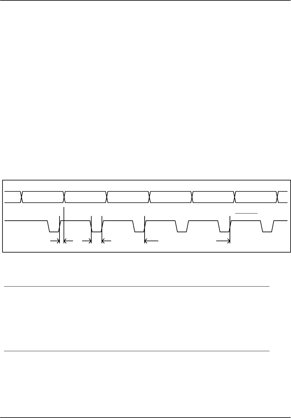
Hardware Installation
RVP8 User’s Manual
May 2003
2–36
to run the cable over distances as great as ten meters. Please see the RxNet7 User’s Manual for
full details, as this is the recommended approach for driving the (I,Q) data out to an external
device.
If the RVP8’s internal TTL signals are to be used directly, the physical connections must be
made in such a way that no more than 12cm of additional wire length is added at the backplane.
One way to do this would be to plug a custom driver board into an unused RVP8/AUX slot, from
which the IBDxxx signals could be accessed. Another approach would be to mount the RVP8
board(s) in a completely custom backplane enclosure which also includes the user’s equipment
that receives the (I,Q) data stream.
The timing of the clock and data lines is shown in Figure 2–6 for the interval of time after the
start of each transmitted pulse. The 18-bit data bus conveys two special code words at the
beginning of each pulse, followed by (I,Q) for the Burst/COHO sample, followed by (I,Q) from
the receiver. The receiver data continue to flow until the next transmitted pulse restarts the
sequence anew, after a brief (approximately one range bin) clearing period. The data bus can be
sampled on either the falling or rising edge of the clock, as there is an enforced 28ns data hold
time after each rising clock edge. Using the rising clock edge will give the greatest data setup
time, and this is usually preferred.
Figure 2–6: Timing diagram of the (I,Q) Data Stream
New Pulse Code Burst “I” Burst “Q” Bin #1 “I” Bin #1 “Q”
Trigger Code
IBDCLK Data Clock
IBD<17:0> Data Bus
Range Bin Spacing
28ns
Clearing Period
(after last pulse)
82ns
The “New Pulse” code is a unique 18-bit value that signifies the start of each new pulse of data.
This is the only code or data word in which the MSB is zero.
17 16 15 14 13 12 11 10 9 8 7 6 5 4 3 2 1 0
| | | | | | | | | | | | | | | | | | |
| 0 0 0 0 0 0 0 0 0 0 0 0 0 0 0 0 0 0 |
|_______________________________________________________________________|
The “Trigger Code” follows immediately after the “New Pulse” code. It has a “1” in its MSB,
and three different bit fields encoded into its low byte. These fields give information about the
pulse itself. Codes that are not listed below are reserved, and will never appear on the data bus.
17 16 15 14 13 12 11 10 9 8 7 6 5 4 3 2 1 0
| | | | | | | | | | | | | | | | | | |
| 1 0 0 0 0 0 0 0 0 0 | Flags | Bank | Waveform |
|_______________________________________|_______|___________|___________|
The 2-bit “Flags” field tells how this pulse will be used internally by the RVP8. This
information is probably irrelevant to the external data processor, if all that it is doing is
eavesdropping on the received data.

Hardware Installation
RVP8 User’s Manual
May 2003
2–37
01 This is the final pulse of a collection of pulses that will contribute to the next pro-
cessed ray.
The 3-bit “Bank” field tells the major classification of the pulse.
000 Normal pulse
001 Low PRF pulse during Dual-PRF mode
010 Blanked transmitter version of a normal pulse
111 Pulse used for receiver noise measurement (SNOISE Command)
The 3-bit “Waveform” field indicates the minor classification of the pulse.
000 Normal pulse, or first pulse in a multi-part pulse sequence.
001 Indicates that this is an “alternate” pulse. This is the “V” channel for a single-
channel polarization radar in which the receive or transmit polarization alternates
pulse to pulse from “H” to “V”. This is also the longer PRT pulse whenever
DPRT (Dual-PRT) mode is running.
000-111 These incrementing codes will be output for the first eight pulses of any custom
trigger pattern that the user has defined (See Section 6.14). If the custom pattern
is more than eight pulses long, the “111” code will be held until the end of the se-
quence.
The (I,Q) data for the Burst/COHO sample, as well as for the receiver samples, all have the same
floating point format consisting of a 2-bit unsigned exponent (Exp) and 15-bit signed mantissa
(Man).
17 16 15 14 13 12 11 10 9 8 7 6 5 4 3 2 1 0
| | | | | | | | | | | | | | | | | | |
| 1 | Exp | Floating Point Mantissa (Signed) |
|___|_______|___________________________________________________________|
This format does not rely on a “hidden bit” in the mantissa. Rather, the mantissa is simply a
15-bit (generally unnormalized) value between –16384 and +16383, and the encoded floating
point value is:
Value Man 16Exp
Note that the exponent shifts the value not in increments of one bit, but rather, by four bits (by
factors of 16). The mantissa will always be the largest integer (i.e., greatest relative precision)
that will fit into the fifteen available bits.
The overall dynamic range is 90dB while maintaining at least 66dB SNR within each sample.
However, the format also gracefully underflows by allowing the mantissa to become small when
Exp=0. This greatly extends the dynamic range into weak signals for which high relative
precision is not required on each sample. The usable dynamic range of values over the entire
receiver span is therefore approximately 125dB.

Hardware Installation
RVP8 User’s Manual
May 2003
2–31
2.4.2 Example Hookup to a MITEQ “MFS-xxx” STALO
The electrical interface for this STALO uses a 25-pin “D” connector with the following pin
assignments
GROUND on pins 1 and 2.
Four BCD digits of 1KHz, 10KHz, 100KHz, and 1MHz frequency steps, using
Pins <25:22>, <21:18>, <17:14>, <13:10>.
Seven binary bits of representing 10MHz steps, Bits<0:6> on Pins<9:3>.
First configure the IFD pins themselves. Pins 1 and 2 are ground, and are connected with
wirewrap wire to the nearby ground posts. Pins 3 through 25 all are signal pins, so we plug in a
jumper for each of these 23 pins. We will use pinmap uplink protocol, so H3 and H4 are
removed; and a x1 on-board crystal, so H2 is also removed.
In this example we will assume that we wish to control the STALO in 20KHz steps from
1.350GHz to 1.365GHz. This can be done with the following setups from the Mb section:
AFC span– [–100%,+100%] maps into [ 1350000 , 1365000 ]
AFC format– 0:Bin, 1:BCD, 2:8B4D: 2, ActLow: NO
AFC uplink protocol– 0:Off, 1:Normal, 2:PinMap : 2
PinMap Table (Type ’31’ for GND, ’30’ for +5)
–––––––––––––––––––––––––––––––––––––––––––––
Pin01:GND Pin02:GND Pin03:22 Pin04:21 Pin05:20
Pin06:19 Pin07:18 Pin08:17 Pin09:16 Pin10:15
Pin11:14 Pin12:13 Pin13:12 Pin14:11 Pin15:10
Pin16:09 Pin17:08 Pin18:07 Pin19:06 Pin20:05
Pin21:GND Pin22:GND Pin23:GND Pin24:GND Pin25:GND
FAULT status pin (0:None): 0, ActLow: NO
We map the AFC interval into a numeric span from 1350000 to 1365000, and choose the
“8B4D” mixed-radix encoding format. The STALO itself has 1KHz frequency steps, but the
AFC servo will be easier to tune if we intentionally degrade this to 20KHz. This is done simply
by grounding all four of the 1KHz BCD input lines, plus the LSB of the 10KHz BCD digit. A
more creative use for one of these unused pins would be to remove the pin 25 jumper, wirewrap
pin 25 to ground (so the STALO sill reads it a logic low), and assign pin 25 as a fault status
input. That pin could then be connected to an external fault line, if the STALO has one.

Hardware Installation
RVP8 User’s Manual
May 2003
2–32
2.5 RVP8 Custom Interfaces
This section describes some additional points of interface to the RVP8. These hookups are less
conventional than the “standard” interfaces described earlier in this chapter, but they sometimes
can supply exactly what is needed in exactly the right place. For the most part, these custom
interfaces are merely taps into existing internal signals that would not normally be seen by the
user.
2.5.1 Using the IFD Coax Uplink
The Coax Uplink is the IFD’s single line of communication from the RVP8/Rx processor board.
All of the information that is needed by the IFD arrives through this uplink; and as such, this
signal might contain information that is also useful for other parts of the radar system. In
particular, it is a convenient source of digital AFC, along with reset and other status bits, plus
limited trigger timing information.
The uplink is a single digital transmission line that carries a hybrid serial protocol. The two
logic states, “zero” and “one” are represented by 0-Volt and +15-Volt (open circuit) electrical
levels. The output impedance of the uplink driver is approximately 55Ω. When the cable is
terminated in 75Ω by an internal resistor in the IFD, the overall positive voltage swing will be
approximately 8.6-Volts.
The electrical characteristics of the uplink have been optimized for balanced “groundless”
reception, so that external noise and ground loop currents will not be introduced into the IFD.
The recommended eavesdropping circuit is shown in Figure 2–4, and consists of a high speed
comparator (Maxim MAX913, or equivalent) and input conditioning resistors. Both the shield
and the center conductor of the coax uplink feed the comparator through 33KΩ isolation
resistors; no direct ground attachment is made to the shield itself. The 500Ω resistors provide
the local ground reference, and the 47KΩ resistor supplies a bias to shift the unipolar uplink
signal into a bipolar range for the comparator.
Figure 2–4: Recommended Receiving Circuit for the Coax Uplink
Max913
or equiv.
33K
33K
500
500
47K
Received
TTL
Signal
+5V
GND
GND
Coax
Uplink
Input

Hardware Installation
RVP8 User’s Manual
May 2003
2–33
The uplink signal, shown in Figure 2–5, is periodic at the radar pulse repetition frequency, and
conveys two distinct types of information to the IFD. The signal is normally low most of the
time (to minimize driver and termination power), but begins a transition sequence at the
beginning of each transmitted pulse.
Figure 2–5: Timing Diagram of the IFD Coax Uplink
12 345678910...
burst sssss
The first part of each pulse sequence is a variable length “burst window” which is centered on
the transmitted pulse itself, and which has a duration burst approximately 800ns greater than the
length of the current FIR matched filter. The burst window defines the interval of time during
which the IFD transmits digitized burst pulse samples, rather than digitized IF samples, on its
fiber downlink. The exact placement and width of the burst window will depend on the trigger
timing and digital filter specifications that the user has chosen, usually via the Pb and Ps plotting
setup commands.
Following the burst window is a fixed-length sequence of 25 serial data bits which convey
information from the RVP8/Rx board. The first four data bits form a characteristic (0,1,1,0)
marker pattern. The first zero in this pattern effectively marks the end of the variable length
burst window, and the other three bits should be checked for added confidence that a valid bit
sequence is being received. Table 2–9 defines the interpretation of the serial data bits.
Table 2–9: Bit Assignments for the IFD Coax Uplink
Bit(s) Meaning
1–4 Marker Sequence (0,1,1,0). This fixed 4-bit sequence identifies the start
of a valid data sequence following the variable-length burst window.
5–20 16-bit multi-purpose data word, MSB is transmitted first (See below)
21 Reset Request. This bit will be set in just one transmitted sequence
whenever an RVP8 reset occurs.
22 If set, then interpret the 16-bit data word as 4-bits of command and
12-bits of data, rather than as a single 16-bit quantity (See below)
23–24 Diagnostic select bits. These are used by the RVP8 power-up diagnostic
routines; they will both be zero during normal operation.
25 Green LED Request; 0=Off, 1=On. The state of this bit normally
follows the “Fiber Detect” LED on the RVP8/Rx board.

Hardware Installation
RVP8 User’s Manual
May 2003
2–34
The period s of the serial data is (64faq), where faq is the acquisition clock frequency given
in the Mc section of the RVP8 setup menu. For the default clock frequency of 35.975MHz, the
period of the serial data will be 1.779µsec. The logic that is receiving the serial data should first
locate the center of the first data bit at (0.5 s) past the falling edge at the end of the burst
window. Subsequent data bits are then sampled at uniform s intervals.
The actual data sampling rate can be in error by as much as one part in 75 while still maintaining
accurate reception. This is because the data sequence is only 25-bits long, and hence, the last
data bit would still be sampled within 1/3 bit time of its center. Having this flexibility makes
it easier to design the receiving logic. For example, if a 5MHz or 10MHz clock were available,
then sampling at 1.8µsec intervals (1:85 error) would be fine. Likewise, one could sample at
1.75µsec based on a 4MHz or 8MHz clock (1:61 error), but only if the first sample were moved
slightly ahead of center so that the sampling errors were equalized over the 25-bit span.
Interpreting the Serial 16-bit Data Word
The serial 16-bit data word has several different interpretations according to how the RVP8 has
been configured, and whether Bit #22 of the uplink stream is set or clear. The evolution of these
different formats has been in response to new features being added to the IFD (Section 2.2), and
the production of the DAFC Digital AFC Module (Section 2.4).
The original use of the uplink data word was simply to convey a 16-bit AFC level, generally for
use with a magnetron system. Bit #22 is clear in this case, and the word is interpreted as a linear
signed binary value. The use of this format is discouraged for new hardware designs, but it will
always remain available to guarantee compatibility with older equipment.
15 14 13 12 11 10 9 8 7 6 5 4 3 2 1 0
| | | | | | | | | | | | | | | | |
| 16–Bit AFC Level | AFC–16
|_______________________________________________________________|
Level 0111111111111111 (most positive AFC voltage)
0000000000000000 (center AFC voltage)
1000000000000000 (most negative AFC voltage)
When the IFD is jumpered for phase locking to an external reference clock, then Bit #22 will be
clear and the data word conveys the PLL clock ratio, and the Positive/Negative deviation sign of
the Voltage Controlled Crystal Oscillator (VCXO). This format is commonly used with klystron
systems, especially when the RVP8 is locking to an external trigger.
15 14 13 12 11 10 9 8 7 6 5 4 3 2 1 0
| | | | | | | | | | | | | | | | |
| |Pos| Numerator – 1 | Denominator – 1 | PLL–16
|___|___|___________________________|___________________________|
Note that the AFC-16 and PLL-16 formats can never be interleaved for use at the same time,
since there would be no way to distinguish them at the receiving end.
Finally, an expanded format has been defined to handle all future requirements of the serial
uplink. Bit #22 is set in this case, and the data word is interpreted as a 4-bit command and 12-bit
data value. A total of 16x12=192 auxiliary data bits thus become available via sequential
transmission of one or more of these words. The CMD/DATA words can also be used along
with one of the AFC-16 or PLL-16 formats, since Bit #22 marks them differently.

Hardware Installation
RVP8 User’s Manual
May 2003
2–35
15 14 13 12 11 10 9 8 7 6 5 4 3 2 1 0
| | | | | | | | | | | | | | | | |
| Command | Data | CMD/DATA
|_______________|_______________________________________________|
Commands #1, #2, and #3 control the 25 output pin levels of the DAFC board. These
transmissions may be interspersed with the PLL-16 format in systems that require both clock
locking and AFC, e.g., a dual-receiver magnetron system using a digitally synthesized COHO.
Note that the entire 25-bits of pin information are transferred synchronously to the output pins
only when CMD=3 is received. This assures that momentary invalid patterns will not be
produced upon arrival of CMD=1 or CMD=2 when the output bits are changing.
CMD=1 Data<0> DAFC output pin 25
Data<6> Fault Input is active high
Data<11:7> Which pin to use for Fault Input (0:None)
CMD=2 Data<11:0> DAFC output pins 24 through 13
CMD=3 Data<11:0> DAFC output pins 12 through 1
These three digital AFC pinmap commands are recommended as a replacement for the original
AFC-16 format in all new hardware designs. If you only need 12-bits of linear AFC, then map
the AFC range into the –2048 to +2047 numeric span, and select binary coding format (See
Section 3.3.6); the 12-bit data with CMD=3 will then hold the required values. To get a full
16-bit value, use a –32768 to +32767 span and extract the full word from both CMD=2 and
CMD=3. Of course, other combinations of bit formats and number of bits (up to 25) are also
possible.
Command #4 is used to control some of the internal features of the IFD. Bits <4:0> configure
the on-board noise generator so that it adds a selectable amount of dither power to the A/D
converters. This noise is bandlimited using a 10-pole lowpass filter so that most of the energy is
within the 150KHz to 900KHz band, with negligible residual power above 1.4MHz. Each of the
five bits switch in additional noise power when they are set, with the upper bits making
successively greater contributions. Bits <6:5> permit the IF-Input and Burst-Input signals to be
reassigned on the fiber downlink.
CMD=4 Data<4:0> Built-in noise generator level
Data<6:5> IF-Input and Burst-Input selection
00 : Normal 01 : Swap IF/Burst
10 : Burst Always 11 : IF Always
2.5.2 Using the (I,Q) Digital Data Stream (Alan)
The (I,Q) data stream that is computed by the FIR filter chips is communicated in real time to
the central CPU. The “IBD<17:0>” data bus and “IBDCLK” clock signals are sourced on the P3
96-pin DIN connector of the RVP8. These TTL signals are normally kept internal to the RVP8,
but some users may have a need to tap into them directly, e.g., to feed a separate data processor
with the demodulated “I” and “Q”.
Making the electrical connections to the (I,Q) data stream is especially easy with the RxNet7
packaging of the RVP8, since the complete set of signals are driven onto a dedicated 68-pin
connector on its backpanel. Moreover, special PECL drivers on that connector make it possible

Hardware Installation
RVP8 User’s Manual
May 2003
2–36
to run the cable over distances as great as ten meters. Please see the RxNet7 User’s Manual for
full details, as this is the recommended approach for driving the (I,Q) data out to an external
device.
If the RVP8’s internal TTL signals are to be used directly, the physical connections must be
made in such a way that no more than 12cm of additional wire length is added at the backplane.
One way to do this would be to plug a custom driver board into an unused RVP8/AUX slot, from
which the IBDxxx signals could be accessed. Another approach would be to mount the RVP8
board(s) in a completely custom backplane enclosure which also includes the user’s equipment
that receives the (I,Q) data stream.
The timing of the clock and data lines is shown in Figure 2–6 for the interval of time after the
start of each transmitted pulse. The 18-bit data bus conveys two special code words at the
beginning of each pulse, followed by (I,Q) for the Burst/COHO sample, followed by (I,Q) from
the receiver. The receiver data continue to flow until the next transmitted pulse restarts the
sequence anew, after a brief (approximately one range bin) clearing period. The data bus can be
sampled on either the falling or rising edge of the clock, as there is an enforced 28ns data hold
time after each rising clock edge. Using the rising clock edge will give the greatest data setup
time, and this is usually preferred.
Figure 2–6: Timing diagram of the (I,Q) Data Stream
New Pulse Code Burst “I” Burst “Q” Bin #1 “I” Bin #1 “Q”
Trigger Code
IBDCLK Data Clock
IBD<17:0> Data Bus
Range Bin Spacing
28ns
Clearing Period
(after last pulse)
82ns
The “New Pulse” code is a unique 18-bit value that signifies the start of each new pulse of data.
This is the only code or data word in which the MSB is zero.
17 16 15 14 13 12 11 10 9 8 7 6 5 4 3 2 1 0
| | | | | | | | | | | | | | | | | | |
| 0 0 0 0 0 0 0 0 0 0 0 0 0 0 0 0 0 0 |
|_______________________________________________________________________|
The “Trigger Code” follows immediately after the “New Pulse” code. It has a “1” in its MSB,
and three different bit fields encoded into its low byte. These fields give information about the
pulse itself. Codes that are not listed below are reserved, and will never appear on the data bus.
17 16 15 14 13 12 11 10 9 8 7 6 5 4 3 2 1 0
| | | | | | | | | | | | | | | | | | |
| 1 0 0 0 0 0 0 0 0 0 | Flags | Bank | Waveform |
|_______________________________________|_______|___________|___________|
The 2-bit “Flags” field tells how this pulse will be used internally by the RVP8. This
information is probably irrelevant to the external data processor, if all that it is doing is
eavesdropping on the received data.

Hardware Installation
RVP8 User’s Manual
May 2003
2–37
01 This is the final pulse of a collection of pulses that will contribute to the next pro-
cessed ray.
The 3-bit “Bank” field tells the major classification of the pulse.
000 Normal pulse
001 Low PRF pulse during Dual-PRF mode
010 Blanked transmitter version of a normal pulse
111 Pulse used for receiver noise measurement (SNOISE Command)
The 3-bit “Waveform” field indicates the minor classification of the pulse.
000 Normal pulse, or first pulse in a multi-part pulse sequence.
001 Indicates that this is an “alternate” pulse. This is the “V” channel for a single-
channel polarization radar in which the receive or transmit polarization alternates
pulse to pulse from “H” to “V”. This is also the longer PRT pulse whenever
DPRT (Dual-PRT) mode is running.
000-111 These incrementing codes will be output for the first eight pulses of any custom
trigger pattern that the user has defined (See Section 6.14). If the custom pattern
is more than eight pulses long, the “111” code will be held until the end of the se-
quence.
The (I,Q) data for the Burst/COHO sample, as well as for the receiver samples, all have the same
floating point format consisting of a 2-bit unsigned exponent (Exp) and 15-bit signed mantissa
(Man).
17 16 15 14 13 12 11 10 9 8 7 6 5 4 3 2 1 0
| | | | | | | | | | | | | | | | | | |
| 1 | Exp | Floating Point Mantissa (Signed) |
|___|_______|___________________________________________________________|
This format does not rely on a “hidden bit” in the mantissa. Rather, the mantissa is simply a
15-bit (generally unnormalized) value between –16384 and +16383, and the encoded floating
point value is:
Value Man 16Exp
Note that the exponent shifts the value not in increments of one bit, but rather, by four bits (by
factors of 16). The mantissa will always be the largest integer (i.e., greatest relative precision)
that will fit into the fifteen available bits.
The overall dynamic range is 90dB while maintaining at least 66dB SNR within each sample.
However, the format also gracefully underflows by allowing the mantissa to become small when
Exp=0. This greatly extends the dynamic range into weak signals for which high relative
precision is not required on each sample. The usable dynamic range of values over the entire
receiver span is therefore approximately 125dB.

RVP8 User’s Manual
April 2003 TTY Nonvolatile Setups (draft)
3–1
3. TTY Nonvolatile Setups (draft)
The RVP8 provides an interactive setup menu that can be accessed either from a serial TTY, or
from the host computer interface. Most of the RVP8’s operating parameters can be viewed and
modified with this menu, and the settings can be saved in non-volatile RAM so that they take
effect immediately on power-up. This permits custom trigger patterns, pulsewidth control,
matched FIR filter specs, PRF, etc., to be configured by the user in the field.
The TTY menu also gives access to a collection of graphical setup and monitoring procedures
that use an ordinary oscilloscope as a synthesized visual display. The burst pulse and receiver
waveforms can be examined in detail (both in the time and frequency domain) and the digital
FIR filter can be designed interactively to match the characteristics of the transmitted pulse.
3.1 Overview of Setup Procedures
This section describes basic operations within the setup menus such as making TTY connections,
entering and exiting the menus, and saving and restoring the configurations.
The setup TTY should be plugged into the modular 6-pin phone jack located at the top edge of
the RVP8 board. The electrical interface may be either RS232 or RS423. If the phone jack
connection is inconvenient, the terminal may be wired directly to the TIOXMT and TIORCV
signals on the P2 96-pin connector. The TTY should be configured for 7-bit or 8-bit data (the
MSB is always zeroed), no parity, and either one or two stop bits.
With jumper JP4 in the ”AB” position, the interface runs at 9600 baud; in the ”BC” position the
rate is 1200 baud (factory default), or some other rate set via the menu. Thus, the ”AB” setting
always makes a reliable 9600 baud connection, even if the the alternate rate is accidently set to a
bad or forgotten value. Note: the reliable 9600 baud rate requires that the crystal located at X1
have a frequency of 4.9152MHz.
3.1.1 Initial Entry and Help List
The interactive setup menu is invoked by pressing the Escape key on the TTY. If that key can
not be found on the keyboard, you can sometimes use Control “[” to generate the ESC code.
The RVP8 then responds with the following banner and command prompt.
SIGMET Incorporated, USA
RVP8 Digital IF Signal Processor Rev.A/01
–––––––––––––––––––––––––––––––––––––––––
RVP8>
The banner identifies the RVP8 product, and gives the hardware version of the board (e.g.,
Rev.A) and software version (e.g., 01). This information is important whenever RVP8 support is
required, and it is also repeated in the printout of the “V” command (See below).
The “Q” command is used to exit from the menus and to restart the RVP8 with the (possibly
changed) set of current values. It is important to quit from the menus before attempting to
resume normal RVP8 operation. Portions of the RVP8 command interpreter remain running
while the menus are active (so that the TTYOP command works properly), but the processor as a
whole will not function until the menus are exited.

RVP8 User’s Manual
April 2003 TTY Nonvolatile Setups (draft)
3–2
From the command prompt, typing “help” or “?” gives the following list of available
commands.
Command List:
F: Use Factory Defaults
S: Save Current Settings
R: Restore Saved Settings
M: Modify/View Current Settings
Mb – Burst Pulse and AFC
Mc – Board Configuration
Mf – Clutter Filters
Mp – Processing Options
Mt<n> – Trigger/Timing <for PW n>
Mz – Transmitter Phase Control
M+ – Debug Options
P: Plot with Oscilloscope
Pb – Burst Pulse Timing
Ps – Burst Spectra and AFC
Pr – Receiver Waveforms
P+ – Visual Test Pattern
V: View Jumpers and Status
?: Cmd list (?? Settings list)
*: Reboot <Max Slaves> <+>
~: Swap Burst/IF Inputs on IFD
Q: Quit
3.1.2 Factory, Saved, and Current Settings
The current settings are the collection of setup values with which the RVP8 is presently
operating; the saved settings are the collection of values stored in non-volatile RAM. The saved
settings are restored (made current) each time the RVP8 is powered up. The “S” command saves
the current settings into the non-volatile RAM, and the “R” command restores those non-volatile
values so that they become the current settings. The “F” command initializes the current settings
with factory default values. Thus, “F” followed by “S” saves factory defaults in non-volatile
RAM, so that the RVP8 powers up in its original configuration as shipped.
The RVP8 retains all of its saved settings when new ROM upgrades are installed; the new
version of code will automatically use all of the previous saved values. However, if the RVP8
detects that the new release requires a setup parameter that did not exist in the previous release,
then a factory default value will automatically be filled in for that parameter. A warning is
printed whenever this occurs (See also, Section 3.1.4).
There is also support for intermediate minor releases of RVP8 code. Each ROM has a major
version number (the one that it always had), plus a minor version number for intermediate
”unofficial” releases. The minor number starts from zero at the time of each ”official” release,
and then increments until the next ”official” release. The RVP8 includes the minor release

RVP8 User’s Manual
April 2003 TTY Nonvolatile Setups (draft)
3–3
number (if it is not zero) in the printout of the ”V” command. Likewise, the minor release
number of the code that last saved the nonvolatile RAM is also shown. This is an improvement
over having to check the date of the code to determine which minor release was running.
Note that the RVP8 does not actually begin using the current settings until after the “Q”
command is entered, so that the processor exits the TTY setup mode and returns to normal
operation.
3.1.3 Processor Reset Command
The “*” command may be used to reset the signal processor from the TTY. This can be handy
when the other methods of reset (power-up, parallel interface reset signal, or SCSI bus reset) can
not easily be done. The command is robust in that pressing the Escape key followed by “*”,
followed by two Returns, always resets the RVP8. There are certain wait conditions from which
a TTY ESC does not immediately enter the setup monitor. However, the above four-key
sequence always forces a full reset.
The RVP8 diagnostics can run in a continuous loop that is useful during production burn–in
testing. In this mode the complete set of powerup tests is repeated approximately once per
second. The green LEDs on the RVP8/Main and RVP8/AUX boards will blink on each run as a
progress indicator. All red LEDs will initially be on, but each will begin to blink if any
diagnostic ever fails on that board. A line of text is also printed to the setup TTY to show the
progress of the tests and a summary of any errors.
The RVP8’s Perpetual Diagnostic Loop maintains a histogram of receiver IF-Input noise levels
in 1dB steps from –85dBm to –72dBm. You can view the accumulated noise distribution by
typing “N” while the diagnostic loop is running. This feature is intended for use during factory
burn-in and testing of RVP8/IFD units.
This special test mode can be started in two ways. One is to powerup the processor with the
RVP8/Main I/O jumpers JP17–JP22 in the (somewhat illegal) pattern: JP17:BC, JP18:BC,
JP19:AB, JP20:AB, JP21:AB, JP22:AB. This method has the advantage of not requiring a TTY
connection. The second method is to reset the processor from the local TTY monitor using the
”*+” command. This is the normal reset command, but with a plus sign (debugging) suffix.
3.1.4 V — View Internal Status
The “V” command allows you to view some internal status within the RVP8. This information
is available for inspection only, and can not be changed from the TTY. The view listing begins
with the banner:
Jumpers and Internal Status
–––––––––––––––––––––––––––
and then prints the following lines:
Rev.B board, ROM V14.12 from Mon Jul 12 19:29:07 1999
This line shows the revision level of the RVP8 board, the ROM code version, and the
date and time that this release was compiled. This lets you know the age of the
release, even if the release notes have been misplaced. The date can also be helpful
in keeping track of “unofficial” interim releases.

RVP8 User’s Manual
April 2003 TTY Nonvolatile Setups (draft)
3–4
Values were last saved using ROM version V14
This line tells which version of RVP8 code was the last to write into the non-volatile
RAM. It is printed only if that last version was different from the ROM version that
is currently running. The information is included so that a “smart upgrade” can often
be done, i.e., values that did not exist in the prior release can be filled in with a guess
that is better than merely taking the factory default.
Warning: 3 automatic defaults were inserted.
This warning will appear (accompanied by a beep) if one or more automatic factory
defaults were required when the non-volatile RAM was last restored. It is likely that
these automatic defaults will be acceptable operating values; but it would be wise to
check the release notes to see what new parameters were added, and to decide on
their proper settings. The warning will disappear once the S command is issued.
This is because the missing saved slots are then filled in with valid values.
Diagnostics: PASS Slave DSP Count: 3
If errors were detected by the powerup diagnostics then an error bitmask will be
shown on the first line. The word “PASS” indicates that no errors were detected.
The slave DSP count is also shown, which is the number of processors that were
detected during the powerup sequence (and which will be used during subsequent
processing). The RVP8 main board has three slave DSPs, and the each RVP8/AUX
board supplies ten more. Up to two RVP8/AUX boards may be attached at the same
time (23 slave DSPs total) for extremely intensive processing applications.
An itemized list (consisting of bit pattern and text) is printed whenever any of the
powerup diagnostics fail. The possible messages that might appear are:
0x00000001 : No fiber downlink signal detected
0x00000002 : 16–Bit AFC level read/write
0x00000004 : IF Receiver reset request not sent
0x00000008 : I/O FIFO full before 4096 writes
0x00000010 : I/O FIFO not full after 4096 writes
0x00000020 : Transmit phase latch bits
0x00000040 : Downlink local counter test
0x00000080 : Receiver status bits & switches
0x00000100 : Test byte pattern from receiver
0x00000200 : Test word pattern from receiver
0x00000400 : Non–Volatile RAM 0x00 and 0xFF flags
0x00000800 : UART read/write check
0x00001000 : External RAM check
0x00002000 : SCSI controller chip error
0x00004000 : Range mask RAM and addressing
0x00008000 : I&Q FIFO interrupt & trigger flags
0x00010000 : I&Q FIFO data bits
0x00020000 : FIR processing of ramp pattern
0x00040000 : Boot words not accepted by first slave
0x00080000 : No reply slave DSP count
0x00100000 : Invalid count of slave DSPs
0x00200000 : Global communication port tests

RVP8 User’s Manual
April 2003 TTY Nonvolatile Setups (draft)
3–5
0x00400000 : Internal tests failed on some slave
0x00800000 : Trigger Generator RAM and addressing
0x01000000 : Excessive coax/fiber round trip jitter
0x02000000 : No sync found in round trip test
0x04000000 : Internal error in compile/link
Coax/Fiber/Pipeline Delay: 0.624 usec (Stdev: 0.014 usec)
During bootup the RVP8 measures the round trip delay along 1) the coax uplink to
the receiver module, 2) the pipeline delays within the receiver module, 3) the optical
fiber downlink to the main board, and 4) pipeline delays in the data decoding
hardware. The time shown is accurate to within 14ns, and is used internally to insure
that the absolute calibration of trigger and burst pulse timing remains unaffected by
the distance between the main board and the receiver module. You may freely splice
any lengths of coax and fiber without affecting the calibrations; the delay time will
change, but the trigger and burst calibrations will remain constant.
The standard deviation of the measured delay is also shown. If the coax uplink and
fiber downlink cables are run properly this variation should be less than the period of
the acquisition clock, e.g., 0.028 sec for the standard 35.975MHz rate. Larger
errors may indicate a problem in the cabling. A diagnostic error bit is set if the error
is greater than two acquisition clock periods.
IFD:Okay, Burst Pwr:–48.6 dBm, Freq:35.975 MHz
This line summarizes the receiver status and Burst input signal parameters. The
status may show:
Okay RVP8/IFD and connecting cables are all working properly
NoFiber Problem in DownLink fiber cable from RVP8/IFD ––> RVP8/Main
UpErr Problem in UpLink COAX cable from RVP8/Main ––> RVP8/IFD
NoPLL RVP8/IFD PLL is not locked to external user-supplied clock reference
DiagSW RVP8/IFD test switches are not in their normal operating position
Reset by: Software Up–time: 0–days 00:49:22
This line lists the origin of the last processor reset, as well as the total time that has
elapsed since that reset occurred. The running time is given in days, followed by
hours : minutes : seconds. The timer wraps around after approximately 180-days of
continuous operation. The cause of the last reset will be one of the following:
1) Power-Up 2) External RESET line
3) SCSI Bus Reset 4) RESET OpCode with “Pwr” bit
5) RESET OpCode with “Rst” bit 6) RESET OpCode with “Dig” bit
7) BOOT OpCode 8) Internal Watchdog
9) TTY “*” command 10) IFD Power Sequencing
11) Burn-In Self Tests
3.1.5 Burst-In / IF-In Swap Command
The “~” command swaps the Burst and IF inputs at the IFD. Requests to toggle the state are
made from the top level as follows:

RVP8 User’s Manual
April 2003 TTY Nonvolatile Setups (draft)
3–6
RVP8> ~
IFD Burst/IF Inputs are: SWAPPED
RVP8> ~
IFD Burst/IF Inputs are: NORMAL
The selection remains in effect for the duration of the setup session, but then returns to
NORMAL upon exiting the TTY monitor. The “~” command is very handy because it allows
the Pb, Pr, and Ps plotting commands to easily run with one input or the other. Here are two
examples of how this might be useful.
When checking the range alignment on a Klystron system, the Pb plot can not be
used in the usual way to center the Tx burst because a continuous-wave COHO
(rather than a burst pulse) is typically used as the phase reference in these
systems. However, if you swap the Burst and IF inputs, you can then use the Pb
command to view and center the received leakage of the Tx pulse, and thus locate
range zero.
When setting up the AFC loop, you can use your RF signal generator to simulate
the transmitter’s frequency, and then run the loop with swapped RVP8/IFD
inputs. The AFC servo will then hunt and follow the siggen frequency supplied
via the receiver. You can then make step changes in that frequency to verify that
the loop responds properly.
Note that the same input swapping function is also available via the RVP8/IFD toggle switches.
However, those switches may be located far away from the operator’s terminal; hence, the
command interface is still a valuable addition. The “~” command can only be used with the new
Rev.D RVP8/IFD; the command is unimplemented, and will not even show up in the “Help” list,
when earlier receivers are connected.

RVP8 User’s Manual
April 2003 TTY Nonvolatile Setups (draft)
3–7
3.2 Host Computer I/O Debugging
The RVP8 supports two very powerful monitoring functions that are helpful in debugging the
I/O interface to the host computer. One examines the physical layer of the interface, i.e., the
electrical handshake and data lines themselves. The other examines the application layer, i.e.,
the 16-bit opcodes and data that define the RVP8’s application programming interface.
3.2.1 Physical-Level I/O Examiner
The RVP8 has TTY support for debugging the physical level of the host computer’s SCSI or
Parallel interface. The “X” (eXamine) command allows you to watch all incoming 16-bit words
as they arrive from the host computer. In addition, you may also send 16-bit words back the
other way. The “X” command is only available from the RS232 hardware TTY interface; it can
not (obviously) be used via chat mode over the same I/O interface that it trying to examine. As
such, the “X” command will not even be listed in the RVP8’s top level help menu during a chat
mode session.
While the “X” command is running, any words that arrive from the computer will immediately
be printed in hex format, along with an “address” (word counter, starting from zero) at the start
of each line. Meanwhile, the “W” subcommand can be used to write individual words back to
the computer, and the “Q” subcommand will exit the I/O examiner entirely.
Note: When the “X” command is running, the RVP8 does not interpret the
incoming 16-bit words as commands and arguments. Data sent to the RVP8 are
discarded after being printed; and output from the RVP8 will occur only if the
“W” subcommand is manually used. The “X” command is intended to debug
the physical layer of the computer interface in a very controlled manner.
The following dialog was captured in response to the host computer writing 100, 200, 300
(decimal) to the RVP8. The “W” subcommand was then used twice to output a 0x4000 and
0x8000 from the RVP8, and the computer then sent the values 1, 2, 3, 4, 5.
RVP8> X
Host Computer I/O Debug Monitor
–––––––––––––––––––––––––––––––
Q: Exit the monitor
W: Output a word to the computer
0x0000: 0x0064 0x00C8 0x012C
Output Word : 0x4000
Output Word : 0x8000
0x0003: 0x0001 0x0002 0x0003 0x0004 0x0005
3.2.2 Application-Level I/O Examiner
The RVP8 has TTY support for debugging the application level of the host computer’s SCSI or
Parallel interface. The Real Time TTY Monitor (RTM, see Section 3.3.7) can be configured to
expose the computer’s complete I/O stream while the RVP8 is running and processing
commands in its normal manner. Because of the enormous amount of TTY output that can be

RVP8 User’s Manual
April 2003 TTY Nonvolatile Setups (draft)
3–8
generated by this option, all other RTM selections are disabled whenever host computer I/O is
being monitored. Also, those other RTM selections would interfere with the multi-line
formatting of the I/O text.
The TTY printout shows incoming opcodes called out by name, and subsequent input and output
words formatted into a table. The data are printed in Hex, twelve words per line, and include a
word offset (origin zero) at the start of each line. The offset is reset to zero at the start of each
new input or output sequence.
Lines of data that are repeats of identical values will be skipped with a “...” indication. This
shortens and simplifies the printout; but more importantly, it reduces TTY overhead so that the
processor is less I/O bound. Also for this reason, the “0x” Hex prefix is omitted during the
possibly lengthy printing of the data word tables.
Note: As with all other Real Time TTY Monitor (RTM) functions, the RVP8
remains completely functional while host computer I/O is being monitored.
However, unlike all other RTM functions, the I/O monitor will stall the main
processor whenever the TTY becomes I/O bound; and the performance of the
RVP8 will be degraded, perhaps severely. It is recommended that you configure
the TTY for 38.4-KBaud to minimize the serial I/O delays.
The following sample transactions were captured in response to starting the IRIS/Open ZAUTO
utility. An I/O RESET and diagnostic OTEST are first performed. The pulse width selection
bits and maximum trigger rates are then set with PWINFO, and angle sync is disabled with
LSYNC. The header words for processed data are decided using CFGHDR, operational
parameters are loaded with SOPRM, and final RVP8 parameters are read back with GPARM.
Finally, the trigger rate is set using SETPWF, and a dummy range mask consisting of a single
bin is setup with LRMSK.
Opcode 0x008C (RESET)
Opcode 0x0004 (OTEST)
Output Words
0: 0001 0002 0004 0008 0010 0020 0040 0080 0100 0200 0400 0800
12: 1000 2000 4000 8000
Opcode 0x000F (PWINFO)
Input Words
0: 8421 012C 0BB8 0FA0 1F40
Opcode 0x0011 (LSYNC)
Opcode 0x005F (CFGHDR)
Input Words
0: 0001 0000
Opcode 0x0002 (SOPRM)
Input Words
0: 0019 000F 07AE 0008 FE70 0080 00A0 0000 0003 000A AAAA 8888
12: C0C0 C000 0000 0000 0000 AAAA 0000 2710
Opcode 0x0009 (GPARM)
Output Words
0: 1200 0001 0960 FFFF FFFF 0D5B 0000 0000 0000 4284 0000 0000
12: 0019 743D 0007 0000 0000 230B 0032 5DC0 0BB8 1770 1D4C 2EE0
24: 8421 0000 2EE0 2EE0 0960 0960 000F 07AE 0008 FE70 0080 00A0
36: 0000 0000 0000 0000 0000 0000 0001 000E 0000 000E 0000 0D5B
48: 8000 0000 0000 0000 0000 0000 0000 0000 0000 0000 0000 0000
60: 0000 0000 0000 0000

RVP8 User’s Manual
April 2003 TTY Nonvolatile Setups (draft)
3–9
Opcode 0x0010 (SETPWF)
Input Words
0: 2EE0
Opcode 0x0001 (LRMSK)
Input Words
0: 0001 0000 0000 0000 0000 0000 0000 0000 0000 0000 0000 0000
12: ...
504: 0000 0000 0000 0000 0000 0000 0000 0000
This RTM option to monitor computer I/O is automatically disabled at powerup, and therefore
can not be saved permanently. This is to avoid confusing situations in which the monitor is
accidently left running –– the RVP8 would appear to be working, but at a puzzling level of
degraded performance.

RVP8 User’s Manual
April 2003 TTY Nonvolatile Setups (draft)
3–10
3.3 View/Modify Dialogs
The M command may be used to view, and optionally to modify, all of the current settings. The
current value of each parameter is printed on the screen, and the TTY pauses for input at the end
of the line. Pressing Return advances to the next parameter, leaving the present one unchanged.
You may also type U to move back up in the list, and Q to exit from the list at any time.
Typing a numeric or YES/NO response (as appropriate to the parameter) changes the
parameter’s value, and displays the line again with the new value. All numbers are entered in
base ten, and may include a decimal point and minus sign. In some cases, several parameters are
displayed on one line, in which case, as many parameters are changed as there are new values
entered. In all cases, the numbers are checked to be within reasonable bounds, and an error
message (listing those bounds) is printed if the limits are exceeded. Note that changes to the
settings (generally) do not take effect until after the Q command is typed, at which point the
RVP8 exits the local TTY menu and resumes its normal processing operations.
Since the number of setup questions is large, follow the M command with a second letter to
select the subcategory, i.e., Mb (Burst Pulse and AFC), Mc (Board Configuration), Mf (Clutter
Filters), Mp (Processing Options), Mt (Triggers and Timing), Mz (Transmitter Phase Control),
M* (Stand-alone Settings) or M+ (Debug Options). The M command by itself prints the entire
set of questions so that you can make a hard copy.
The M command always works from the current parameter values, not from the saved values in
non-volatile RAM. If the host computer has modified some of the current values, then you will
see these changes as you skip through the setup list. However, typing S at that point would save
all of the current settings and would, perhaps, make many changes to the original non-volatile
settings. In general, to make an incremental change to the saved settings, first type R to restore
all of the saved values, then use M to make the changes starting from that point, and S to save
the new values.
A listing of the parameters that can be viewed and modified with the M command is detailed in
the following subsections. In each case, the line of text is shown exactly as it appears on the
TTY with the factory default settings. A definition of each parameter is given and, if applicable,
the lower and upper numeric bounds are shown.
3.3.1 Mc — Board Configuration
This set of commands configure general properties of the RVP8/IFD and RVP8/Main boards.
Acquisition clock: 35.9751 MHz
This is the frequency of the oscillator at U5 in the IF receiver module. Except for
custom receivers, this will always be 35.9751 MHz; which gives a fundamental
sample spacing of 1/240 km (approximately 4.17 meters).
Limits: 33.33 to 41.67 MHz
Dual simultaneous receivers are being used: NO
Answer this question “Yes” if the RVP8 will be processing simultaneous signals from
two separate receivers. Answering “No” will revert to normal operation with just a
single receiver.

RVP8 User’s Manual
April 2003 TTY Nonvolatile Setups (draft)
3–11
Dual–LNA/Rcvr single–channel switched mode: NO
For dual-polarization single-receiver systems, this question decides whether you have
a single LNA and IF-Amplifier that switches between H&V (the typical case); or two
separate receivers, each hard wired to H and V, with switching performed after the IF
amplifiers. The question affects how noise levels are measured and applied to the
data.
Synthesize LOG video output waveform: YES
Upper 100.0 dB will occupy 85.0% of voltage span
Force freerunning video mode: NO
Plot data from secondary receiver: NO
The RVP8 supports the option of sourcing a LOG Video analog output signal from
the backpanel of the main chassis. There are two ways that this signal can be
configured:
Self-Triggering, Free-Running Mode
This is the default mode that is available on all RVP8 boards. The output signal
is periodic at approximately the PRF of the radar, but is free-running, i.e., not
actually synchronized with the radar trigger. A synthetic 1.0 sec wide, full
scale, “trigger” pulse is embedded at the zero-range start of each LOG Video
waveform. This marker can easily trigger an oscilloscope if the scope’s trigger
level is set just below the maximum LOG Video voltage level.
Waveform Locked to Radar Trigger
This mode requires a (one-wire) hardware modification to the Rev.B RVP8/Main
board. The LOG Video waveform then becomes locked to the radar trigger, so
that the LOG signal can be displayed on any device that already receives the radar
trigger.
In either case, the LOG Video output signal is unipolar, ranging from approximately
0.0V to 3.0V. It is active during all data processing modes that the host computer
might request, as well as during the idle time between scans. The signal is absent
(zero), however, during the short intervals of time that the RVP8 is being
reconfigured by the host computer, or when the RVP8’s local TTY setups are being
used.
The time resolution of the synthesized LOG Video signal is fixed at 1.0 sec per bin.
This is independent of the actual range resolution of the FIR matched filter.
Whatever (I,Q) data are actually being computed by the FIR front end are selected for
a nearest fit to each 1.0 sec synthetic output cell. The maximum number of
incoming FIR range bins that can be selected among is 5460. Thus, for example, the
maximum range of the LOG Video signal would be 682km when the FIR range
resolution is 125–meters.
Answer the first question “Yes” if you would like the RVP8/Main board to
synthesize and drive the LOG Video output signal. The cost of doing this is that one
of the “slave” DSP chips will be removed from the normal Doppler processing chain,
and dedicated to the task of LOG Video generation. On a single-board system, the

RVP8 User’s Manual
April 2003 TTY Nonvolatile Setups (draft)
3–12
three available slave DSPs would be reduced to two; whereas on a dual-board system,
the 13 available DSPs would be reduced to 12. Obviously, the percentage penalty is
less in a larger system.
The second question decides how the overall dynamic range of the receiver will fit
into the 12-bit unipolar output voltage span of the DAC that produces the LOG Video
waveform. The default setting calls for the upper 100dB of dynamic range to occupy
85% of the output voltage span. This means that the strongest IF input signal would
produce 85% of the maximum DAC voltage (approximately 2.55 Volts); 50dB down
would be 42.5%, and 100dB down would be 0%, i.e., zero volts.
If you are using a self-triggering LOG Video waveform, then the 15% of headroom
provided by the default settings leaves room for the embedded trigger pulse.
However, if your RVP8 has the hardware modification required to synchronize the
LOG Video to the system trigger, then the full 100% of the DAC voltage span can
freely be used. The third setup question can be used to force freerunning mode on an
RVP8 that has the hardware modification. This question is included mostly for
testing purposes.
The last question only appears in dual-receiver mode. Answer “Yes” if you would
like the LOG video analog output signal to be based on the data from the secondary
receiver rather than from the primary receiver.
Scope plots– Holdoff ratio: 0.50, Stroke: 1000.0 usec
The oscilloscope plotting commands are described in Chapter 4. This question
allows you to vary the amount of holdoff time that is inserted between each drawing
stroke, as well as the stroke length itself. Try increasing the holdoff if your scope is
not triggering reliably. Longer holdoffs make it easier for the scope to find the initial
trigger point, but may introduce visible flicker. To reduce flicker, try decreasing the
stroke duration from its default value of 1000 microseconds.
Limits: Holdoff 0.05 to 5.00, Stroke 100 to 10000 sec.
PWINFO command enabled: No
The “Pulsewidth Information” user interface command can be disabled, thus further
protecting the radar against inappropriate combinations of pulsewidth and PRF. This
is a more safe setting in general, and is even more important when DPRT triggers are
being generated. It can also be useful when running user code that is not yet fully
debugged.
TRIGWF command enabled: NO
The “Trigger Waveform” user interface command can be disabled if you want to
prevent the host computer from overwriting the RVP8’s stored trigger specifications.
This is the default setting, based on the assumption that the built-in plotting
commands would be used to configure the triggers. Answering “YES” will allow
new waveforms to be loaded from the host computer.
RVP7 Emulation: No
The RVP8 implements a reasonably precise emulation of the RVP7 command set.
This mode is useful because it allows an RVP8 to be plugged directly into a software
system that used to run with an RVP7. All of the configuration steps that are new and

RVP8 User’s Manual
April 2003 TTY Nonvolatile Setups (draft)
3–13
unique to the RVP8 can be handled by the local TTY and Scope setups, thus making
no demands on the user’s system code for support. Answer this question “YES” for
maximum compatibility with old driver software. However, if you are running IRIS
version 6.11 or higher, then answer “NO” to enable using new RVP8 features as they
are developed.
The RVP8 returns a version number of 35 when the processor is running in RVP7
compatibility mode. This fudged value will appear in the SCSI Inquiry Command
reply, and in the GPARM parameter packet. Elsewhere, the correct RVP8 ROM
version number will always appear. The reason for doing this is so that the RVP8
appears (to the host computer) to be a modern RVP7 with all of the latest opcodes
and features.
3.3.2 Mp — Processing Options
Major Mode- 0:User, 1:PPP, 2:FFT : 0
The top level RVP8 operating modes are described in the documentation of SOPRM
command word #9. This question allows you to use the mode that has been selected
by that command, or to force the use of a particular mode.
Window- 0:User, 1:Rect, 2:Hamming, 3:Blackman : 0
Whenever power spectra are computed by the RVP8, the time series data are
multiplied by a (real) window prior to computation of the Fourier Transform. You
may use whichever window has been selected via SOPRM word #10, or force a
particular window to be used.
R2 Processing- 0:Never, 1:User, 2:Always : 1
Controls R0/R1 versus R0/R1/R2 processing. Selecting ”0” unconditionally disables
the R2 algorithms, regardless of what the host computer requests in the SOPRM
command. Likewise, selecting ”2” unconditionally enables R2 processing. These
choices allow the RVP8 to run one way or the other without having to rewrite the
user code. This is useful for compatibility with existing applications.
Clutter Microsuppression- 0:Never, 1:User, 2:Always : 1
Controls whether individual “cluttery” bins are rejected prior to being averaged in
range. Same interpretation of cases as for ”R2 Processing” above.
2D Final Speckle/Unfold – 0:Never, 1:User, 2:Always : 1
The Doppler parameter modes (PPP, FFT, etc) include an optional 3x3 interpolation
and speckle removal filter that is applied to the final output rays. This 2-dimensional
filter examines three adjacent range bins from three successive rays in order to assign
a value to the center point. Thus, for each output point, its eight neighboring bins in
range and time are available to the filter. Only the dBZ, dBT, Vel, and Width data are
candidates for this filtering step; all other parameters are processed using the normal
1-dimensional (three bins in range) speckle remover. See Section 5.3.3 for more
details.

RVP8 User’s Manual
April 2003 TTY Nonvolatile Setups (draft)
3–14
Unfold Velocity (Vh–Vl) – 0:Never, 1:User, 2:Always : 0
This question allows you to choose whether the RVP8 will unfold velocities using a
simple (Vhigh – Vlow) algorithm, rather than the standard algorithm described in
Section 5.6. Bit-11 of SOPPRM word #10 is the host computer’s interface to this
function when the “1:User” case is selected (See Section 6.3).
Note: This setup question is included for research customers only. The standard
unfolding algorithm should still be used in all operational systems because of its
lower variance. For this reason, the factory default value of this parameter is
“0:Never”.
Process w/ custom trigs – 0:Never, 1:User, 2:Always : 0
This question allows you to choose whether the RVP8 will attempt to run its standard
processing algorithms even when a custom trigger pattern has been selected via the
SETPWF command. Generally it does not make sense to do this, so the default
setting is “0:Never”. Bit-12 of OPPRM word #10 is the host computer’s interface to
this function when the “1:User” case is selected (See Section 6.3).
Minimum freerunning ray holdoff: 100% of dwell
This parameter controls the rate at which the RVP8 processes free-running rays in the
FFT, DPRT, and Random Phase modes. This prevents rays from being produced at
the full CPU limit or I/O limit of the processor (whichever was slower); which could
result in highly overlapping data being output at an unusably fast rate. Note that this
behavior will only occur when one of these non-PPP modes is chosen, and is then
allowed to run without angle syncing. Such is likely the case for IRIS manual scans
or during Passive IRIS mode.
To make these free-running modes more useful, you may establish a minimum
holdoff between successive rays, expressed as a percentage of the number of pulses
contributing to each ray. Choosing 100% (the default) will produce rays whose input
data do not overlap at all, i.e., whose rate will be exactly the PRF divided by the
sample size. Choosing 0% will give the unregulated behavior in which no minimum
overlap is enforced and rays may be produced very quickly.
Limits: 0 to 100%
Linearized saturation headroom: 4.0 dB
The RVP8 uses a statistical saturation algorithm that estimates the real signal power
correctly even when the IF receiver is overdriven (i.e., for input power levels above
+4dBm). The algorithm works quite well in extending the headroom above the top
end of the A/D converter, although the accuracy decreases as the overdrive becomes
more severe. This parameter allows you to place an upper bound on the maximum
extrapolation that will ever be applied. Choosing 0dB will disable the algorithm
entirely.
Limits: 0 to 6dB
Apply amplitude correction based on Burst/COHO: YES
Time constant of mean amplitude estimator: 70 pulses
The RVP8 can perform pulse-to-pulse amplitude correction of the digital (I,Q) data
stream based on the amplitude of the Burst/COHO input. Please see Section 5.1.6 for
a complete discussion of this feature.

RVP8 User’s Manual
April 2003 TTY Nonvolatile Setups (draft)
3–15
Limits: 10 to 500 pulses
IFD built–in noise dither source: –57.0dBm
This question will only appear if the processor is attached to a Rev.D RVP8/IFD that
includes an out-of-band noise generator to supply dither power for the A/D
converters. The available power levels are { Off, –57dBm, –37dBm, –32dBm,
–27dBm, –22dBm, –19dBm }. The closest available level to your typed-in value will
be used. You can observe the band-limited noise easily in the Pr plot to confirm its
amplitude and spectral properties.
For standard operation, we recommend running at –57dBm. The problem higher
levels of dither level is that, for certain choices of (I,Q) FIR filter, the stopband of the
filter may not give enough attenuation to preserve the RVP8/IFD’s inherent noise
level. For example, the factory default 1MHz bandwidth Hamming filter has a
stopband attenuation near DC of approximately 43dB. You can see this graphically at
the right edge of the Ps menu. The in-band contribution of dither power is therefore
approximately (–37dBm) – 43dB = –80dBm, which exceeds the A/D converter’s
1MHz bandwidth noise of –81.5dBm.
TAG bits to invert AZ:0000 EL:0000
TAG scale factors AZ:1.0000 EL:1.0000
TAG offsets (degrees) AZ:0.00 EL:0.00
The incoming TAG input bits may be selectively inverted via each of the 16-bit
words. The values are displayed in Hex. Setting a bit will cause the corresponding
AZ (bits 0–15) or EL (bits 16–31) lines to be inverted. Note that the SOPRM
command also specifies TAG bits to invert. Both specifications are XOR’ed together
to yield the net inversion for each TAG line.
The overall operations are performed in the order listed. Incoming bits are first
inverted according to the two 16-bit XOR masks. This yields an unsigned 16-bit
integer value which is then multiplied by the signed scale factor. The result is
interpreted as a 16-bit binary angle (in the low sixteen bits), to which the offset angle
is finally added.
As an example, suppose that the elevation angle input to the RVP8 was in an
awkward form such as unsigned integer tenths of degrees, i.e., 0x0000 for zero
degrees, 0x000a for one degree, 0x0e06 for minus one degree, etc. If we apply a
scale factor of 65536/3600 = 18.2044 to these units, we will get 16-bit binary angles
in the standard format. If we further suppose that the input angle rotated
“backwards”, we could take care of this too using a multiplier of –18.2044.
Interference Filter– 0:None, Alg.1, Alg.2, Alg.3: 1
Threshold parameter C1: 10.00 dB
Threshold parameter C2: 12.00 dB
The RVP8 can optionally apply an interference filter to remove impulsive-type noise
from the demodulated (I,Q) data stream. See Section 5.1.4 for a complete description
of this family of algorithms.

RVP8 User’s Manual
April 2003 TTY Nonvolatile Setups (draft)
3–16
Polarization Params – Filtered:YES NoiseCorrected:YES
PhiDP – Negate: NO , Offset:0.0 deg
KDP – Length: 5.00 km
T/Z/V/W computed from: H–Xmt:YES V–Xmt:YES
T/Z/V/W computed from: Co–Rcv:YES Cx–Rcv:NO
The first question decides whether all polarization parameters will be computed from
filtered or unfiltered data, and whether noise correction will be applied to the power
measurements.
The second and third questions define the sign and offset corrections for DP and the
length scale for KDP.
The fourth and fifth questions control how the standard parameters (Total
Reflectivity, Corrected Reflectivity, Velocity, and Width) are computed in a multiple
polarization system. Answering YES to H-Xmt and/or V-Xmt means that data from
those transmit polarizations should be used whenever there is more than one choice
available. Thus, these selections only apply to the Alternating and Simultaneous
transmit modes. Likewise, answering YES to Co-Rcv and/or Cx-Rcv means to use the
received data from the co-channel or cross-channel. The receiver question will only
appear when dual simultaneous receivers have been configured.
A typical installation might use H-Xmt:YES, V-Xmt:YES, Co-Rcv:YES, Cx-Rcv:NO.
This will compute (T/Z/V/W) from the co-polarized receiver using both H&V
transmissions. Including both transmissions will decrease the variance of (T/Z/V/W);
although some researchers prefer excluding V-Xmt because that is more standard in
the literature. Also, if your polarizations are such that the main power is returned on
the cross channel, then you will probably want Co-Rcv:NO and Cx-Rcv:YES.
DualRx – Sum H+V Time Series: NO
In dual-receiver systems, you may choose whether the (H+V) time series data consist
of the sum of the “H” and “V” samples or the concatenation of half the “H” samples
followed by half the “V” samples. The later is more useful when custom software is
being used to analyze the data from the two separate receive channels.
3.3.3 Mf — Clutter Filters
Doppler Filter Set- 0:40dB, 1:50dB, 2:Saved : 0
The RVP8 has two built-in IIR Doppler clutter filter sets; one set having 40dB of
stopband attenuation, and the other having 50dB. This question chooses which set is
loaded on powerup.

RVP8 User’s Manual
April 2003 TTY Nonvolatile Setups (draft)
3–17
Spectral Clutter Filters
––––––––––––––––––––––––
Filter #1 – Type:0(Fixed) Width:1 EdgePts:2
Filter #2 – Type:0(Fixed) Width:2 EdgePts:2
Filter #3 – Type:0(Fixed) Width:3 EdgePts:3
Filter #4 – Type:0(Fixed) Width:4 EdgePts:3
Filter #5 – Type:1(Variable) Width:1 EdgePts:2 Hunt:2
Filter #6 – Type:1(Variable) Width:2 EdgePts:2 Hunt:2
Filter #7 – Type:1(Variable) Width:3 EdgePts:3 Hunt:3
These questions define the heuristic clutter filters that operate on power spectra
during the FFT-type major modes. Filter #0 is reserved as “all pass”, and is not
redefinable here. For filters #1 through #7, enter a digit to choose the filter type,
followed by however many parameters that type requires.
Fixed Width Filters (Type 0)
These are defined by two parameters. The “Width” sets the number of spectral points
that are removed around the zero velocity term. A width of one will remove just the
DC term; a width of two will remove the DC term plus one point on either side; three
will remove DC plus two points on either side, etc. Spectral points are removed by
replacing them with a linear interpolating line. The endpoints of this line are
determined by taking the minimum of “EdgeMinPts” past the removed interval on
each side.
Variable Width, Single Slope (Type 1)
The RVP8 supports variable-width frequency-domain clutter filters. These filters
perform the same spectral interpolation as the fixed-width filters, except that their
notch width automatically adapts to the clutter. The new filters are characterized by
the same Width and EdgePts parameters in the Mf menu, except that the Width is now
interpreted as a minimum width. An additional parameter Hunt allows you to choose
how far to extend the notch beyond Width in order to capture all of the clutter power.
Setting Hunt=0 effectively converts a variable-width filter back into a fixed-width
filter.
The algorithm for extending the notch width is based on the slope of adjacent spectral
points. Beginning (Width–1) points away from zero, the filter is extended in each
direction as long as the power continues to decrease in that direction, up to adding a
maximum of Hunt additional points. If you have been running with a fixed Width=3
filter, you might try experimenting with a variable Width=2 and Hunt=1 filter.
Perhaps the original fixed width was actually failing at times, but you were reluctant
to increase it just to cover those rare cases. In that case, try selecting a variable
Width=2 and Hunt=2 filter as an alternative. In general, make your variable filters
“wider” by increasing Hunt rather than increasing Width. This will preserve more
flexibility in how they can adapt to whatever clutter is present.
Residual clutter LOG noise margin: 0.15 dB/dB
Whenever a clutter correction is applied to the reflectivity data, the LOG noise
threshold needs to be increased slightly in order to continue to provide reliable
qualification of the corrected values. The reason for this is that the uncertainty in the
corrected reflectivity becomes greater after the clutter is subtracted away.

RVP8 User’s Manual
April 2003 TTY Nonvolatile Setups (draft)
3–18
For example, if we observe 20dB of total power above receiver noise, and then apply
a clutter correction of 19dB, we are left with an apparent weather signal power of
+1dB above noise. However, the uncertainty of this +1dB residual signal is much
greater than that of a pure weather target at the same +1dB signal level.
The “Residual Clutter LOG Noise Margin” allows you to increase the LOG noise
threshold in response to increasing clutter power. In the previous example, and with
the default setting of 0.15dB/dB, the LOG threshold would be increased by 19x0.15
= 2.85dB. This helps eliminate noisy speckles from the corrected reflectivity data.
Whitening Parameters
––––––––––––––––––––
Noise threshold for replacing a point: 1.20
Replacement value multiplier: 0.5000
SNR in tails, for determining width: 0.25
These questions control the adaptive whitening filter that is used by the Random
Phase processing algorithms. A spectral point will be whitened if the ratio of its
power to the noise power exceeds the “Noise threshold for replacing a point.” The
whitened point will consist of a complex value whose ARG is identical to that of the
original point, and whose MAG is the product of the noise level with the
“Replacement value multiplier” term. The nominal spectral width of the whitened
region is a function of the power and width of the coherent signal, and the noise
level. Assuming a Gaussian model, the “SNR in tails...” value is the ratio of the
coherent power in the tails of the distribution to the noise level.
RPhase SQI Threshold Slope:0.50 Offset:–0.05
The two values in this question define a secondary SQI threshold that is used to
qualify the LOG data during Random Phase processing. The secondary SQI level is
computed by multiplying the primary user-supplied SQI threshold by the SLOPE,
and adding the OFFSET. See also Section 5.9.3.
Limits: SLOPE: 0.0 to 2.0, OFFSET –2.0 to 1.0
3.3.4 Mt — General Trigger Setups
These questions are accessed by typing “Mt” with no additional arguments. They configure
general properties of the RVP8 trigger generator
Pulse Repetition Frequency: 500.00 Hz
This is the Pulse Repetition Frequency of the internal trigger generator.
Limits: 50 to 6000Hz.
Transmit pulse width: 0
Limits: 0 to 3
Use external pretrigger: NO
PreTrigger active on rising edge: YES
PreTrigger fires the transmitter directly: NO
When an external pretrigger is applied to the TRIGIN input of the RVP8, either the
rising or falling edge of that signal initiates operation. This decision also affects
which signal edge becomes the reference point for the pretrigger delay times given in
the “Mt<n>” section.

RVP8 User’s Manual
April 2003 TTY Nonvolatile Setups (draft)
3–19
Answer the second sub-question according to whether the radar transmitter is directly
fired by the the external pretrigger, rather than by one of the RVP8’s trigger outputs.
In other words, answer “YES” if the transmitter would continue running fine even if
the RVP8 TRIGIN signal were removed. This information is used by the ”L” and
”R” subcommands of the ”Pb” plotting command, i.e., when slewing left and right to
find the burst pulse, the pretrigger delay will be affected rather than the start times of
the six output triggers.
2–way (Tx+Rx) total waveguide length: 0 meters
Use this question to compensate for the offset in range that is due to the length of
waveguide connecting the transmitter, antenna, and receiver. You should specify the
total 2-way length of waveguide, i.e., the span from transmitter to antenna, plus the
span from antenna to receiver. The RVP8 range selection will compensate for the
additional waveguide length to within plus-or-minus half a bin, and works properly at
all range resolutions.
POLAR0 is high for vertical polarization : NO
POLAR1 is high for vertical polarization : NO
These questions define the logical sense of the two polarization control signals
POLAR0 and POLAR1. In a dual-polarization radar POLAR0 should be used to
select one of two possible states (nominally horizontal and vertical, but any other
polarization pair may also be used). The control signal will either remain at a fixed
level, or will alternate from pulse to pulse with a selectable transition point (See
Section 3.3.5). POLAR1 is identical to POLAR0, but may be configured with a
different polarity and switch point. This second signal could be used if the radar’s
polarization switch required more than one control line transition when changing
states.
Quantize trigger PRT to ((1 x AQ) + 0) clocks
It is possible to control the exact quantization of the PRT of the internal trigger
generator. Normally the trigger PRT is chosen as the closest multiple of AQ (the
acquisition clock period) that approximates the requested period. This question
allows the possible PRT’s to be constrained to ((N x AQ) + M) clock cycles. This
feature can be useful for synchronous receiver systems in which the trigger period
must be some exact multiple of the COHO period.
Blank output triggers according to TAG#0 : NO
Blank when TAG input is high : NO
Blank triggers 1:YES 2:YES 3:YES 4:YES 5:YES 6:YES
These questions control trigger blanking based on the TAG0 input line. You first
select whether the trigger blanking feature is enabled; and then optionally choose the
polarity of TAG0 that will result in blanking, and which subset of the six user
definable triggers are to be blanked.
Blank output triggers during noise measurement : NO
The RVP8 can inhibit the subset of blankable trigger lines whenever a noise
measurement is taken. This will be forced whenever trigger blanking (based on
TAG0) is enabled, but it can also be selected in general via this question. Since noise
triggers must be blanked whenever trigger blanking is enabled, this question only
appears if trigger blanking is disabled.

RVP8 User’s Manual
April 2003 TTY Nonvolatile Setups (draft)
3–20
This question permits the state of the triggers during noise measurements to be
consistent and known, regardless of whether the antenna happens to be within a
blanked sector; and you have the additional flexibility of choosing blanked noise
triggers all the time.
Rx–Fixed Triggers: #1:N #2:N #3:N #4:N #5:N #6:N P0:N P1:N Z:N
You have explicit control over which RVP8 trigger outputs are timed relative to the
transmitter pre-fire sequence, versus those which are relative to the actual received
target ranges. Triggers in the first category will be moved left/right by the “L/R”
keys in the Pb plot, and will also be slewed in response to Burst Pulse Tracking.
Triggers in the second category remain fixed relative to “receiver range zero”, and
are not affected by the “L/R” keys or by tracking.
This question specifies which triggers are Tx-relative and which are Rx-relative.
Answer with a sequence of “Y” or “N” responses for each of the six trigger lines, for
the two polarization control lines, and for the timing of the phase control lines. You
should answer No for any trigger that is involved with the pre-fire timing of the
transmitter. If you enable the Burst Pulse Tracker (Section 5.1.3) you will probably
want to assign a Yes to some of your triggers so that they remain fixed relative to the
burst itself.
It is very helpful to have these two categories of trigger start times. Triggers that fire
the transmitter, either directly or indirectly, should all be moved as a group when
hunting for the burst pulse and moving it to the center of the FIR window. However,
triggers that function as range strobes should be fixed relative to range zero, i.e., the
center of that window, and the center of the burst. This distinction becomes
important when the transmitter’s pre-fire delay drifts with time and temperature.
Replace triggers with alternate waveforms: YES
Trigger #1 – 0:Normal, 1–2:Pol0–1, 3–6:PW0–3 : 0
Trigger #2 – 0:Normal, 1–2:Pol0–1, 3–6:PW0–3 : 0
Trigger #3 – 0:Normal, 1–2:Pol0–1, 3–6:PW0–3 : 0
Trigger #4 – 0:Normal, 1–2:Pol0–1, 3–6:PW0–3 : 1
Trigger #5 – 0:Normal, 1–2:Pol0–1, 3–6:PW0–3 : 0
Trigger #6 – 0:Normal, 1–2:Pol0–1, 3–6:PW0–3 : 4
These questions make it possible to reassign the waveforms that are driven onto the
six user trigger (TRIG1–6) BNC outputs on the backpanel of the RVP8. This makes
it easier to adapt the external cabling of the RVP8 so as to make better use of the
available BNC connectors and related 15V drivers. You may substitute either of the
two polarization control lines or the four pulsewidth control lines in place of any of
the six normal triggers.
In the example above, triggers #1, #2, #3, and #5 are all driven with their normal
waveforms. However trigger #4 will have a copy of the POLAR0 polarization
control line, and trigger #6 will have a copy of the PWBW1 pulsewidth control line.
Neither POLAR0 nor PWBW1 themselves are changed by these assignments.
Whenever any of the six user trigger lines is reassigned from its normal setting, the
plot of that trigger within the Pb command will show a hashed line across the screen.
This is a graphical reminder that that trigger has been replaced by some other
waveform.

RVP8 User’s Manual
April 2003 TTY Nonvolatile Setups (draft)
3–21
Merge triggers to create composite waveforms: YES
Merge Trigger #1 into : #1: #2: #3: #4: #5: #6:
Merge Trigger #2 into : #1: #2: #3: #4: #5: #6:
Merge Trigger #3 into : #1:Y #2: #3: #4: #5: #6:
Merge Trigger #4 into : #1: #2:Y #3: #4: #5: #6:
Merge Trigger #5 into : #1: #2:Y #3: #4: #5: #6:
Merge Trigger #6 into : #1: #2: #3: #4: #5: #6:
These questions allow you to merge the six user triggers together; resulting in trigger
patterns that can be much more complex. In this example, Trigger #3 will be merged
into Trigger #1; Trigger #3 will be unaltered, and Trigger #1 will be the “OR” of
itself with Trigger #3. Likewise, Triggers #4 and #5 will be merged into Trigger #2
so that the later will contain three distinct pulses within each PRT. Answer each
question with a sequence of up to six “Y” or “N” responses in order to set the merged
destinations for each trigger line.
Note that the six triggers are still defined in the usual way in the Mt<n> menu, i.e.,
start time, width, etc. The only change is that you may now combine these individual
pulse definitions into a more complex composite output waveform.
3.3.5 Mt<n> — Triggers for Pulsewidth #n
These questions are accessed by typing “Mt”, with an additional argument giving the pulsewidth
number. They configure specific trigger and FIR bandpass filter properties for the indicated
pulsewidth only.
Trigger #1 – Start: 0.00 usec
#1 – Width: 1.00 usec High:YES
Trigger #2 – Start: 0.00 usec + ( 0.500000 * PRT )
#2 – Width: 10.00 usec High:YES
Trigger #3 – Start: –3.00 usec
#3 – Width: 1.00 usec High:YES
Trigger #4 – Start: –2.00 usec
#4 – Width: 1.00 usec High:YES
Trigger #5 – Start: –1.00 usec
#5 – Width: 1.00 usec High:YES
Trigger #6 – Start: –5.00 usec + (–0.001000 * PRT )
#6 – Width: 2.00 usec High:NO
These parameters list the starting times (in microseconds relative to range zero), the
widths (in microseconds), and the active sense of each of the six triggers generated by
the internal trigger generator. Setting a width to zero inhibits the trigger on that line.
The Start Time can include an additional term consisting of the pulse period times a
fractional multiplier between –1.0 and +1.0. This allows you to produce trigger
patterns that would not otherwise be possible, e.g., a trigger that occurs half way

RVP8 User’s Manual
April 2003 TTY Nonvolatile Setups (draft)
3–22
between every pair of transmitted pulses, and remains correctly positioned regardless
of changes in the PRF Enter this multiplier as “0” if you do not wish to use this term,
and it will be omitted entirely from the printout..
In the above example, Trigger #2 is a 10.0 sec active-high pulse whose leading edge
occurs precisely halfway between the zero-range of every pair of pulses. Likewise,
Trigger #6 is a 2.0 sec active-low pulse whose falling edge is nominally 5.0 sec
prior to range zero, but which is advanced by 1.0 sec for every millisecond of
trigger period. All other triggers behave normally, and have fixed starting times that
do not vary with trigger period.
Some subtleties of these variable start times are:
The PRT multipliers can only be used in conjunction with the RVP8’s internal
trigger generator. The PRT-relative start times are completely disabled whenever
an external trigger source is chosen from the Mt menu.
When PRT-relative triggers are plotted by the Pb command, the active portion of
the trigger will be drawn cross-hatched and at a location computed according to
the current PRF. The cross-hatching serves as a reminder that the actual location
of that trigger may vary from it’s presently plotted position.
The PRT multiplier for a given pulse is applied to the interval of time between
that pulse and the next one. This distinction is important whenever the RVP8 is
generating multiple-PRT triggers, e.g., during DPRT mode, or during Dual-PRF
processing. Multipliers from 0.0 to +1.0 are generally safe to use because they
shift the trigger into the same pulse period that originally defined it. For
example, a start time of (0.0 sec + (0.98 * PRT)) would position a trigger 98%
of the way up to the next range zero. But, if –0.98 were used, and if the period of
the previous pulse was shorter than the current one, then that shorter period would
become incorrect (longer) as a result of having to fit in the very early trigger.
A small but important detail is built into the algorithm for producing the six user
trigger waveforms. It applies whenever a) the trigger period is internally determined,
i.e., the external pretrigger input is not being used, and b) the overall span of the six
trigger definitions combined does not fit into that period. What happens in this case
is that any waveforms that do not fit will be zeroed (not output) so that the desired
period is preserved. This means that you can define triggers with large positive start
times, and they will pop into existence only when the PRF is low enough to
accommodate them.
For example, if Trigger #2 is defined as a 200.0sec pulse starting at +400.0sec,
then that trigger would be suppressed if the PRF were 2000Hz, but it would be
present at a PRF of 1000Hz. Whenever a trigger does not completely fit within the
overall period it is suppressed entirely. Thus, even though the +400.0sec start time
is still valid at 2000Hz, the entire 200.0sec pulse would not fit, and so the pulse is
eliminated altogether.
Start limits: –5000 to 5000 sec. Width limits: 0 to 5000 sec.

RVP8 User’s Manual
April 2003 TTY Nonvolatile Setups (draft)
3–23
Maximum number of Pulses/Sec: 2000.0
Maximum instantaneous ’PRF’ : 2000.0 (/Sec)
These are the PRF protection limits for this pulsewidth.
The wording of the “Maximum number of Pulses/Sec” question serves as a reminder
that the number shown is not only an upper bound on the PRF, but also a duty cycle
limit when DPRT mode is enabled.
The “Maximum instantaneous ’PRF’” question allows you to configure the maximum
instantaneous rate at which triggers are allowed to occur, i.e., the reciprocal of the
minimum time between any two adjacent triggers. This parameter is included so that
you can limit the maximum DPRT trigger rate individually for each pulsewidth.
Note that the maximum instantaneous PRF can not be set lower than the maximum
number of pulses per second.
PRF limits: 50 to 20000Hz.
External pretrigger delay to range zero: 3.00 usec
Range Zero is time at which the signal from a target at zero range would appear at the
radar receiver outputs. This parameter adjusts the delay from the active edge of the
external trigger to range zero. It is important that this delay be correct when the
RVP8 is operating with an external trigger, since the zero range point is a fixed time
offset from that trigger. When the transmitter is driven from the internal trigger
signals, those signals themselves are adjusted (see Burst Pulse alignment procedures)
to accomplish the alignment of range zero.
Limits: 0.1 to 500 sec.
Range resolution: 125.00 meters
The range resolution of the RVP8 is determined by the decimation factor of the
digital matched FIR filter that computes “I” and “Q”. This decimation factor is the
ratio of the filter’s input and output data rates, and can be any integer from six to
sixteen. The Acquisition Clock (See Mc Section) sets the input data rate. At its
standard frequency of 35.9751MHz, the available range resolutions (in meters) are:
50.0, 58.3, 66.7, 75.0, 83.3, 91.7, 100.0, 108.3, 116.7, 125.0, and 133.3.
The ranges that are selected by the bit mask in the LRMSK command are spaced
according to the range resolution that is chosen here. Also, the upper limit on the
impulse response length of the matched FIR filter (see below) is constrained by the
range resolution. If you choose a range resolution that can not be computed at the
present filter length, then a message of the form: “Warning: Impulse response
shortened from 72 to 42 taps” will appear.
Limits: 50.0 to 133.3 meters.
FIR-Filter impulse response length: 1.33 usec
The RVP8 computes “I” and “Q” using a digital FIR (Finite Impulse Response)
matched filter. The length of that filter (in microseconds) is chosen here. At the
standard Acquisition Clock rate of 35.9751MHz, a 1.00 microsecond impulse
response corresponds to a filter that is 36 taps long.
The filter length should be based on several considerations:

RVP8 User’s Manual
April 2003 TTY Nonvolatile Setups (draft)
3–24
It should be at least as long as the transmitted pulsewidth. If it were shorter, then
some of the returned energy would be thrown away when “I” and “Q” are
computed at each bin. The SNR would be reduced as a result.
It should be at least as long as the range bin spacing. The goal here is to choose
the longest filter that retains statistical independence among successive bins. If
the filter length is less than the bin spacing, then no IF samples would be shared
among successive bins, and those bins would certainly not be correlated.
It should be “slightly longer” than either of the above bounds would imply, so
that the filter can do a better job of rejecting out-of-band noise and spurious
signals. The SNR of weak signals will be improved by doing this.
In practice, a small degree of bin-to-bin correlation is acceptable in exchange for the
filter improvements that become possible with a longer impulse response. The FIR
coefficients taper off to zero on each end; hence, the power contributed by
overlapping edge samples is minimal. SIGMET recommends beginning with an
impulse response length of 1.2–1.5 times the pulsewidth or bin spacing, whichever is
greater.
The maximum possible filter length is bounded according to the range resolution that
has been chosen; a finer bin spacing leaves less time for computing a long filter. For
the RVP8 Rev.A processor, the filter length must be less than 2.92 sec at 125-meter
resolution; for Rev.B and higher this limit increases to 6.67 sec.
NOTE: Cascade filter software is being contemplated that will extend the maximum
impulse response length to at least 50 sec. This is of interest when very long
(uncoded CW) transmitted pulses are used.
FIR-Filter prototype passband width: 0.503 MHz
This is the passband width of the ideal lowpass filter that is used to design the
matched FIR bandpass filter. The actual bandwidth of the final FIR filter will depend
on 1) the filter’s impulse response length, and 2) the design window used in the
process. The actual 3dB bandwidth will be:
Larger than the ideal bandwidth if that bandwidth is narrow and the FIR length is
too short to realize that degree of frequency discrimination. In these cases it may
be reasonable to increase the filter length.
Smaller than the ideal bandwidth if the FIR length easily resolves the frequency
band. This is because of the interaction within the filter’s transition band of the
ideal filter and the particular design window being used. For example, for a
Hamming window and sufficiently long filter length, the ideal bandwidth is an
approximation of the 6dB (not 3dB) attenuation point. Hence, the 3dB width is
narrower than the ideal prototype width.
This parameter should be tuned using the TTY output and interactive visual plot from
the “Ps” command. The actual 3dB bandwidth is shown there, so that it can be
compared with the ideal prototype bandwidth.
Limits: 0.05 to 10.0 MHz.

RVP8 User’s Manual
April 2003 TTY Nonvolatile Setups (draft)
3–25
Output control 4–bit pattern: 0001
These are the hardware control bits for this pulsewidth. The bits are the 4-bit binary
pattern that is output on PWBW0:3
Bit Limits: 0 to 15 (input must be typed in decimal)
Current noise level: –75.00 dBm
Powerup noise level: –75.00 dBm
–or–
Current noise levels – PriRx: –75.00 dBm, SecRx: –75.00 dBm
Powerup noise levels – PriRx: –75.00 dBm, SecRx: –75.00 dBm
These questions allow you to set the current value and the power-up value of the
receiver noise level for either a single or dual receiver system. The noise level(s) are
shown in dBm, and you may alter either one from the TTY. The power-up level(s)
are assigned by default when the RVP8 first starts up, and whenever the RESET
opcode is issued with Bit #8 set. Likewise, the current noise level is revised
whenever the SNOISE opcode is issued. These setup questions are intended for
applications in which the RVP8 must operate with a reasonable default value, up until
the time that an SNOISE command is actually received. They may also be used to
compare the receiver noise levels during normal operation, which serves as a check
that each FIR filter is behaving as expected when presented with thermal noise.
Transmitter phase switch point: –1.00 usec
This is the transition time of the RVP8’s phase control output lines during random
phase processing modes. The switch point should be selected so that there is
adequate settling time prior to the burst/COHO phase measurement on each pulse.
This question only appears if the PHOUT[0:7] lines are actually configured for phase
control (See Section 3.3.1).
Limits: –500 to 500 sec.
Polarization switch point for POLAR0: –1.00 usec
Polarization switch point for POLAR1: 1.00 usec
The RVP8’s POLAR0 and POLAR1 digital output lines control the polarization
switch in a dual-polarization radar. During data processing modes in which the
polarization alternates from pulse to pulse, the transition points of these control
signals are set by these two questions. The values are in microseconds relative to
range zero; the same units used to define the start times of the six user triggers. The
logical sense of POLAR0 and POLAR1 is set by questions described in Section 3.3.4.
Limits: –500 to 500 sec.
3.3.6 Mb — Burst Pulse and AFC
These questions are accessed by typing “Mb”. They set the parameters that influence the phase
and frequency analysis of the burst pulse, and the operation of the AFC feedback loop.
Receiver Intermediate Frequency: 30.0000 MHz
This is the center frequency of the IF receiver and burst pulse waveform. The RVP8
can operate at an intermediate frequency from any of the three alias bands
22–32MHz, 40–50MHz, and 58–68MHz. These bands are delineated by 4MHz

RVP8 User’s Manual
April 2003 TTY Nonvolatile Setups (draft)
3–26
safety zones on either side of integer multiples of half the RVP8/IFD’s 36MHz
sampling frequency. The value entered here implicitly defines the band, and hence,
the boundaries of the 18MHz window in which the IF is assumed to fall.
Limits: 22 to 68 MHz.
Primary Receiver Intermediate Frequency: 30.0000 MHz
Secondary Receiver Intermediate Frequency: 24.0000 MHz
These alternate questions will replace the previous question whenever the RVP8’s
dual-receiver mode is selected. You should enter the two intermediate frequencies
for your primary and secondary (nominally horizontal and vertical polarized)
receivers. Note that you can easily swap receiver channels merely by exchanging the
two frequency values.
IF increases for an approaching target: YES
The intermediate frequency is derived at the receiver’s front end by a microwave
mixer and sideband filter. The filter passes either the lower sideband or the upper
sideband, and rejects the other. Depending on which sideband is chosen, an increase
in microwave frequency may either increase (STALO below transmitter) or decrease
(STALO above transmitter) the receiver’s intermediate frequency. This question
influences the sign of the Doppler velocities that are computed by the RVP8.
PhaseLock to the burst pulse: YES
This question controls whether the RVP8 locks the phase of its synthesized “I” and
“Q” data to the measured phase of the burst pulse. For an operational magnetron
system this should always be “YES”, since the transmitter’s random phase must be
known in order to recover Doppler data. The “NO” option is appropriate for non
phase modulated Klystron systems in which the RVP8/IFD sampling clock is locked
to the COHO. It is also useful for bench testing in general. In these “NO” cases the
phase of “I” and “Q” is determined relative to the stable internal sampling clock in
the RVP8/IFD module.
Minimum power for valid burst pulse: –15.0 dBm
This is the minimum mean power that must be present in the burst pulse for it to be
considered valid, i.e., suitable for input into the algorithms for frequency estimation
and AFC. The reporting of burst pulse power is described in Section 4.4; the value
entered here should be, perhaps, 8 dB less. This insures that burst pulses will still be
properly detected even if the transmitter power fades slightly.
The mean power level of the burst is computed within the narrowed set of samples
that are used for AFC frequency estimation. The narrow subwindow will contain
only the active portion of the burst, and thus a mean power measurement is
meaningful. The full FIR window would include the leading and trailing pulse edges
and would not produce a meaningful average power. Since radar peak power tends to
be independent of pulse width, this single threshold value can be applied for all
pulsewidths.
Limits: –60 to +10 dBm.
Design/Analysis Window– 0:Rect, 1:Hamming, 2:Blackman : 1
You may choose the window that is used in 1) the design of the FIR matched filter,
and 2) the presentation of the power spectra for the various scope plots. Choices are
rectangular, Hamming, and Blackman; the Hamming window being the best overall

RVP8 User’s Manual
April 2003 TTY Nonvolatile Setups (draft)
3–27
choice. The Blackman window is useful if you are trying to see plotted spectral
components that are more than 40dB below the strongest signal present. It is
especially useful in the “Pr” plot when a long span of data are available. FIR filters
designed with the Blackman window will have greater stopband attenuation than
those designed with the Hamming window, but the wider main lobe may be
undesirable. The rectangular window is included mostly as a teaching tool, and
should never be used in an operational setting.
Settling time (to 1%) of burst frequency estimator: 5.0 sec
The burst frequency estimator uses a 4th order correlation model to estimate the
center frequency of the transmitted pulses. Each burst pulse will typically occupy
approximately one microsecond; yet the frequency estimate feeding the AFC loop
needs to be accurate to, perhaps, 10KHz. Obviously this accuracy can not be
achieved using just one pulse. However, several hundred of the (unbiased) individual
estimates can be averaged to produce an accurate mean. This averaging is done with
an exponential filter whose time constant is chosen here.
Limits: 0.1 to 120 seconds.
Lock IFD sampling clock to external reference: NO
This question determines the usage of the shared SMA connector that is labeled
“AFC/(CLK)” on the RVP8/IFD. It is generally not necessary to phase lock the IFD
sampling clock to the radar system clock, since very good stability is obtained from
the burst phase measurements during normal operation. However, two cases that
benefit from clock locking are 1) using the RVP8 in a klystron system where an
external trigger is provided, and 2) dual-receiver systems in which computation of
DP is important.
The following two questions will appear only if you have requested that the IFD
sampling clock be locked to an external clock reference. See Section 2.2.11 for a
description of the hardware setups that must accompany this selection.
PLL ratio of (1/1) ==> Input reference at 17.9876 MHz
The VCXO phase-locked-loop (PLL) in the RVP8/IFD can work with any input
reference clock whose frequency is a rational multiple (P/Q) of half the desired
sampling frequency, i.e., center frequency of the VCXO. This question allows this
ratio to be established. In general, the best PLL performance will be attained when
the ratio is reduced to lowest terms, e.g., use a ratio of 6/5 rather than 12/10.
Limits: 1 to 128 for both numerator and denominator.
VCXO has positive frequency deviation: YES
Most VCXOs have positive frequency deviation, i.e., their output frequency increases
with increasing input control voltage. This question will generally be answered
“yes”, but is included to accommodate the other case as well. The PLL will not lock,
and will be completely unstable, if the wrong choice is made.
Enable AFC and MFC functions: YES
AFC is required in a magnetron system to maintain the fixed intermediate frequency
difference between the transmitter and the STALO. AFC is not required in a klystron
system since the transmitted pulse is inherently at the correct frequency.

RVP8 User’s Manual
April 2003 TTY Nonvolatile Setups (draft)
3–28
The following rather long list of questions will appear only if AFC and MFC
functions have been enabled.
AFC Servo– 0:DC Coupled, 1:Motor/Integrator : 0
The AFC servo loop can be configured to operate with an external Motor/Integrator
frequency controller, rather than the usual direct-coupled FM control. This type of
servo loop is required for tuned magnetron systems in which the tuning actuator is
moved back and forth by a motor, but remains fixed in place when motor drive is
removed. These systems require that the AFC output voltage (motor drive) be zero
when the loop is locked; and that the voltage be proportional to frequency error while
tracking. Please see Section 3.3.6.1 for more details.
Wait time before applying AFC: 10.0 sec
After a magnetron transmitter is first turned on, it may be several seconds or even
minutes until its output frequency becomes stable. It would not make sense for the
AFC loop to be running during this time since there is nothing gained by chasing the
startup transient. This question allows you to set a holdoff delay from the time that
valid burst pulses are detected to the time that the AFC loop actually begins running.
Limits: 0 to 300 seconds.
AFC hysteresis -- Inner: 5.0 KHz, Outer: 15.0 KHz
These are the frequency error tolerances for the AFC loop. The loop will apply
active feedback whenever the outer frequency limit is exceeded, but will hold a fixed
level once the inner limit has been achieved. The hysteresis zone minimizes the
amount of thrashing done by the feedback loop. The AFC control voltage will
remain constant most of the time; making small and brief adjustments only
occasionally as the need arises.
AFC outer tolerance during data processing: 50.0 KHz
In general, the AFC feedback loop is active only when the RVP8 is not processing
data rays. This is because the Doppler phase measurements are seriously degraded
whenever the AFC control voltage makes a change. To avoid this, the AFC loop is
only allowed to run in between intervals of sustained data processing. This is fine as
long as the host computer allows a few seconds of idle time every few minutes; but if
the RVP8 were constantly busy, the AFC loop would never have a chance to run.
This question allows you to place an upper bound on the frequency error that is
tolerated during sustained data processing. AFC is guaranteed to be applied
whenever this limit is exceeded.
Limits: 15 to 4000 KHz.
AFC feedback slope: 0.0100 D-Units/sec / KHz
AFC minimum slew rate: 0.0000 D–Units/sec
AFC maximum slew rate: 0.5000 D-Units/sec
These questions control the actual feedback computations of the AFC loop.
The overall span of the AFC output voltage is set by Gain and Offset potentiometers
on the RVP8/IFD module (See Section 2.2.10). The control level that is applied to
the AFC’s 16-bit Digital-to-Analog converter is specified here in “D-Units”, i.e.,

RVP8 User’s Manual
April 2003 TTY Nonvolatile Setups (draft)
3–29
arbitrary units ranging from –100 to +100 corresponding to the complete span of the
D/A converter. Since the D–Unit corresponds in a natural way to a percentage scale,
the shorter “%” symbol is sometimes used.
AFC feedback will be applied in proportion to the frequency error that the algorithm
is attempting to correct. The feedback slope determines the sensitivity and time
constant of the loop by establishing the AFC’s rate of change in (D-Units / sec) per
thousand Hertz of frequency error. For example, a slope of 0.01 and a frequency
error of 30KHz would result in a control voltage slew of 0.3 D-Units per second. At
that rate it would take approximately 67 seconds for the output voltage to slew one
tenth of its total span (20 D-Units / (0.3 D-Units / sec) = 67 sec). AFC is intended to
track very slow drifts in the radar system, so response times of this magnitude are
reasonable.
Keep in mind that the feedback slew is based on a frequency error which itself is
derived from a time averaging process (see Burst Frequency Estimator Settling Time
described above) . The AFC loop will become unstable if a large feedback slope is
used together with a long settling time constant, due to the phase lag introduced by
the averaging process. Keep the loop stable by choosing a small enough slope that
the loop easily comes to a stop within the inner hysteresis zone.
See Section 3.3.6.1 for more information about these slope and slew rate parameters.
AFC span– [–100%,+100%] maps into [ –32768 , 32767 ]
AFC format– 0:Bin, 1:BCD, 2:8B4D: 0, ActLow: NO
AFC uplink protocol– 0:Off, 1:Normal, 2:PinMap : 1
The RVP8’s implementation of AFC has been generalized so that there is no
difference between configuring an analog loop and a digital loop. The AFC feedback
loop parameters are setup the same way in each case; the only difference being the
model for how the AFC information is made available to the outside world. Many
types of interfaces and protocols thus become possible according to how these three
questions are answered. AFC output follows these three steps:
The internal feedback loop uses a conceptual [–100%,+100%] range of values.
However, this range may be mapped into an arbitrary numeric span for eventual
output. For example, choosing the span from –32768 to +32767 would result in
16-bit AFC, and 0 to 999 might be appropriate for 3-digit BCD; but any other
span could also be selected from the full 32-bit integer range.
Next, an encoding format is chosen for the specified numeric span. The result of
the encoding step is another 32-bit pattern which represents the above numeric
value. SIGMET will make an effort to include in the list of supported formats all
custom encodings that our customers encounter from their vendors.
Available formats include straight binary, BCD, and mixed-radix formats that
might be required by a specialized piece of equipment. The “8B4D” format
encodes the low four decimal digits as four BCD digits, and the remaining upper
bits in binary. For example, 659999 base-10 would encode into 0x00419999
Hex.
Finally, an output protocol is selected for the bit pattern that was produced by
encoding the numeric value. The bits may be written to the eight RVP8/Main

RVP8 User’s Manual
April 2003 TTY Nonvolatile Setups (draft)
3–30
backpanel RS232 outputs, or sent on the uplink as a value to be received by the
RVP8/IFD and converted to an analog voltage. Yet another option is for the bits
to be sent on the uplink and received by the RVP8/DAFC board, which supports
arbitrary remapping of its output pins.
To summarize: the internal AFC feedback level is first mapped into an arbitrary
numeric span, then encoded using a choice of formats, and finally mapped into an
arbitrary set of pins for digital output. We are hopeful that this degree of flexibility
will allow easy hookup to virtually any STALO synthesizer that one might encounter.
PinMap Table (Type ’31’ for GND, ’30’ for +5)
–––––––––––––––––––––––––––––––––––––––––––––
Pin01:00 Pin02:01 Pin03:02 Pin04:03 Pin05:04
Pin06:05 Pin07:06 Pin08:07 Pin09:08 Pin10:09
Pin11:10 Pin12:11 Pin13:12 Pin14:13 Pin15:14
Pin16:15 Pin17:16 Pin18:17 Pin19:18 Pin20:19
Pin21:20 Pin22:21 Pin23:22 Pin24:23 Pin25:24
FAULT status pin (0:None): 0, ActLow: NO
These questions only appear when the “PinMap” uplink protocol has been selected.
The table assigns a bit from the encoded numeric word to each of the 25 pins of the
RVP8/DAFC module. For example, the default table shown above simply assigns the
low 25 bits of the encoded bit pattern to pins 1-25 in that order. You may also pull a
pin high or low by assigning it to +5 or GND. Note that such assignments produce a
logic-high or logic-low signal level, not an actual power or ground connection. The
latter must be done with actual physical wires.
One of the RVP8/DAFC pins can optionally be selected as a Fault Status indicator.
You may choose which pin to use for this purpose, as well as the polarity of the
incoming signal level. Note that the standard RVP8/DAFC module only supports the
selection of pins 1, 3, 4, 13, 14, and 25 as inputs. This setup question allows you to
choose any pin, however, because it does not know what kind of hardware may be
listening on the uplink and what its constraints might be.
Burst frequency increases with increasing AFC voltage: NO
If the frequency of the transmit burst increases when the AFC control voltage
increases, then answer this question “Yes”; otherwise answer “No”. When this
question is answered correctly, a numerical increase in the AFC drive (D–Units) will
result in an increase in the estimated burst frequency. If the AFC loop is completely
unstable, try reversing this parameter.
Mirror AFC voltage on– 0:None, 1:I, 2:Q : 0
AFC/MFC can be mirrored on a backpanel output of the main chassis using this
question. When either “I” or “Q” is selected, the AFC/MFC voltage will be present
on the corresponding BNC output, and the other output will be used for scope
plotting. This configuration would be useful, for example, in a dual-receiver
magnetron system that needs a phase locked acquisition clock in the RVP8/IFD, but
also needs an AFC tuning voltage to control the transmit frequency. When “None” is
selected, scope plotting will revert to its normal “Q” output.

RVP8 User’s Manual
April 2003 TTY Nonvolatile Setups (draft)
3–31
The voltage range of the “I” and “Q” outputs is approximately 1 Volt, and is not
adjustable. When AFC/MFC is mirrored on these lines, you will probably need to
add an external Op-Amp circuit to adjust the voltage span and offset to match your
RF components. We also recommend that you add significant low-pass filtering
(cutoff at 3Hz) to remove any power line noise or crosstalk that may be originating
within the RVP8/Main chassis.
Enable Burst Pulse Tracking: YES
This question enables the Burst Pulse Tracking algorithm that is described in Section
5.1.3. Remarkably, for such an intricate new feature, there are no additional
parameters to configure. The characteristic settling times for the burst are already
defined elsewhere in this menu, and the tracking algorithm uses dynamic thresholds
to control the feedback.
Enable Time/Freq hunt for missing burst: No
Number of frequency intervals to search: 5
Settling time for each frequency hop: 0.25 sec
Automatically hunt immediately after being reset: YES
Repeat the hunt every: 60.00 sec
These questions configure the process of hunting for a missing burst pulse. The
trigger timing interval that is checked during Hunt Mode is always the maximum
+20sec; hence no further setup questions are needed to define the hunting process in
time. The hunt in frequency is a different matter. The overall frequency range will
always be the full –100% to +100% AFC span; but the number of subintervals to
check must be specified, along with the STALO settling time after making each AFC
change. With the default values shown, AFC levels of –66%, –33%, 0%, +33%, and
+66% will be tried, with a one-quarter second wait time before checking for a valid
burst at each AFC setting.
You should choose the number of AFC intervals so that the hunt procedure can
deduce an initial AFC level that is within a few megaHertz of the correct value. The
normal AFC loop will then take over from there to keep the radar in tune. For
example, if your radar drifts considerably in frequency so that the AFC range had to
be as large as 35MHz, then choosing fifteen subintervals might be a good choice.
The hunt procedure would then be able to get within 2.3MHz of the correct AFC
level. The settling time can usually be fairly short, unless you have a STALO that
wobbles for a while after making a frequency change. Note that hunting in frequency
is not allowed for Motor/Integrator AFC loops, and the two AFC questions will be
suppressed in that case.
The RVP8 can optionally begin hunting for a missing burst pulse immediately after
being reset, but before any activity has been detected from the host computer. This
might be useful in systems that both drift a lot and generally have their transmitter
On. However, this option is really included just as a work around; the correct way
for a burst pulse hunt to occur is via an explicit request from the host computer which
“knows” when the pulse really should be present. Blindly hunting in the absence of
that knowledge can not be done because there are many reasons why the burst pulse
may legitimately be missing, e.g., during a radar calibration.

RVP8 User’s Manual
April 2003 TTY Nonvolatile Setups (draft)
3–32
The automatic hunt for the burst pulse will always run at least once whenever the
feature is enabled. The automatic hunting ceases, however, as soon as any activity is
detected from the host computer. Only use this feature on radars with a serious drift
problem in their burst pulse timing.
Simulate burst pulse samples: NO
The RVP8 can simulate a one microsecond envelope of burst samples. This is useful
only as a testing and teaching aid, and should never be used in an operational system.
A two-tone simulation will be produced when the RVP8 is setup in dual-receiver
mode. The pulse will be the sum of two transmit pulses at the primary and secondary
intermediate frequencies. To make the simulation more realistic, the two signal
strengths are unequal; the primary pulse is 3dB stronger than the secondary pulse.
Frequency span of simulated burst: 27.00 MHz to 32.00 MHz
The simulated burst responds to AFC just as a real radar would. The frequency span
from minimum AFC to maximum AFC is given here.
3.3.6.1 AFC Motor/Integrator Option
The question “AFC Servo– 0:DC Coupled, 1:Motor/Integrator” selects whether the
AFC loop runs in the normal manner (direct control over frequency), or with an
external Motor/Integrator type of actuator. The question “AFC minimum slew
request:...” provides additional control when interfacing to mechanical actuators
whose starting and sustaining friction needs to be overcome.
The DC-Coupled AFC loop questions (changes shown in bold) are:
AFC Servo– 0:DC Coupled, 1:Motor/Integrator : 0
Wait time before applying AFC: 10.0 sec
AFC hysteresis– Inner: 5.0 KHz, Outer: 15.0 KHz
AFC outer tolerance during data processing: 50.0 KHz
AFC feedback slope: 0.0100 D–Units/sec / KHz
AFC minimum slew rate: 0.0000 D–Units/sec
AFC maximum slew rate: 0.5000 D–Units/sec
and the Motor/Integrator loop questions are:
AFC Servo– 0:DC Coupled, 1:Motor/Integrator : 1
Wait time before applying AFC: 10.0 sec
AFC hysteresis– Inner: 5.0 KHz, Outer: 15.0 KHz
AFC outer tolerance during data processing: 50.0 KHz
AFC feedback slope: 1.0000 D–Units / KHz
AFC minimum slew request: 15.0000 D–Units
AFC maximum slew request: 90.0000 D–Units
Notice that the physical units for the feedback slope and slew rate limits are different
in the two cases. In the DC-Coupled case the AFC output voltage controls the
frequency directly, so the units for the feedback and slew parameters use
D-Units/Second. In the Motor/Integrator case, the AFC output determines the rate of
change of frequency; hence D-Units are used directly.
The above example illustrates typical values that might be used with a
Motor/Integrator servo loop. The feedback slope of 1.0 D-Units/KHz means that a
frequency error of 100KHz would produce the full-scale (100 D-Units) AFC output.
But this is modified by the minimum and maximum slew requests as follows:

RVP8 User’s Manual
April 2003 TTY Nonvolatile Setups (draft)
3–33
A zero D-Unit output will always be produced whenever AFC is locked.
When AFC is tracking, the output drive will always be at least 15 D-Units.
This minimum non-zero drive should be set to the sustaining drive level of the
motor actuator, i.e., the minimum drive that actually keeps the motor turning.
When AFC is tracking, the output drive will never exceed 90 D-Units. This
parameter can be used to limit the maximum motor speed, even when the
frequency error is very large.
The AFC Motor/Integrator feedback loop works properly even if the motor has
become stuck in a “cold start”, i.e., after the radar has been turned off for a period of
time. The mechanical starting friction can sometimes be larger than normal, and
additional motor drive is required to break out of the stuck condition. But once the
motor begins to turn at all, then the normal AFC parameters (minimum slew,
maximum slew, feedback slope) all resume working properly. The algorithm
operates as follows:
Whenever AFC correction is being applied, the RVP8 calculates how long it
would take to reach the desired IF frequency at the present rate of change. For
example, if we are 1MHz away from the desired IF frequency, and the measured
rate of change of the IF burst frequency is 20KHz/sec, then it will be 50 seconds
until the loop reaches equilibrium.
Whenever the AFC loop is in Track-Mode, but the time to equilibrium is greater
than two minutes, then the “Minimum Slew” parameter will be slowly increased.
The idea is to gradually increase the starting motor drive whenever it appears that
the IF frequency is not actually converging toward the correct value, i.e., the
motor is stuck.
As soon as the frequency is observed to begin changing, such that the desired IF
would be reached in less than two minutes, then the ”Minimum Slew” parameter
is immediately put back to its correct setup value. The loop then continues to run
properly using its normal setup values.
Manual Frequency Control (MFC) operates unchanged in both of the AFC servo
modes. Whenever MFC is enabled in the Ps command, it always has the effect of
directly controlling the output voltage of the AFC D/A converter. The MFC mode
can be useful when testing the motor response under different drive levels, and when
determining the correct value for the minimum slew request.
3.3.7 M+ — Debug Options
A collection of debugging options has been added to the RVP8 to help users with the
development and debugging of their applications code. For the most part, these options should
remain disabled during normal radar operation. These questions are included so that the RVP8
can be placed into unusual, and perhaps occasionally useful, operating states.

RVP8 User’s Manual
April 2003 TTY Nonvolatile Setups (draft)
3–34
Noise level for simulated data: –50.0 dB
This is the noise level that is assumed when simulated “I” and “Q” data are injected
into the RVP8 via the LSIMUL command. The noise level is measured relative to the
power of a full-scale complex (I,Q) sinusoid, and matches the levels shown on the
slide pots of the ASCOPE digital signal simulator.
Limits: –100dB to 0dB
Simulate output rays: NO
Answering ”YES” to this question causes the RVP8 to output bands of simulated
data. The bands can occupy a selectable range interval, and span a selectable interval
of data values.
Start bin:0, Width:10 bins, Bands:16
This question is only asked if we are simulating output rays. The Start Bin chooses
the bin number (origin zero) where the simulated bands will begin. The width of
each band (in bins), and the total number of bands are also selected. The upper limit
for all parameters is the maximum bin count for the RVP8 (which depends on board
configuration, and number of attached RVP8/AUX boards).
Limits: Start: 0-Max, Width: 1-Max, Bands: 1-Max
Start data value:0, Increment:16
This question is only asked if we are simulating output rays. The data value that will
be assigned to the first simulated band, and the data increment from one band to the
next, are selected. The permissible values are from 0 to 65535, i.e., the full unsigned
16-bit integer range. This full range is useful when simulating 16-bit output data; for
the more typical 8-bit output formats, only the low byte of the start and increment are
significant.
Limits: 0 to 65535
3.3.8 Mz — Transmitter Phase Control
These questions are used to configure the 8-Bit phase modulation codes that may be used to
control the phase of a coherent transmitter. The RVP8 will output a pseudo-random sequence of
phase codes that are chosen from a specified set of available codes, i.e., all 8-bit patterns that are
valid for the phase modulation hardware. The random sequence is output only when the RVP8
is in one of its random phase processing modes (time series or parameter). At all other times, a
fixed “idle” phase code pattern is output. See also Sections 3.3.1 and 3.3.5 where related phase
control questions are found.
8–Bit code to output when idle: 0x00
This is the bit pattern to be output whenever the RVP8 is not in a random phase
processing mode. Note that this “idle” code does not have to be one of the
“active”codes that are enabled below.
Selection of Valid 8-Bit States
–––––––––––––––––––––––––––––––
00–0F: Y – – – – – – – – – – – – – – –

RVP8 User’s Manual
April 2003 TTY Nonvolatile Setups (draft)
3–35
10–1F: – – – – – – – – – – – – – – – –
20–2F: – – – – – – – – – – – – – – – –
30–3F: – – – – – – – – – – – – – – – –
40–4F: – – – – – – – – – – – – – – – –
50–5F: – – – – – – – – – – – – – – – –
60–6F: – – – – – – – – – – – – – – – –
70–7F: – – – – – – – – – – – – – – – –
80–8F: – – – – – – – – – – – – – – – –
90–9F: – – – – – – – – – – – – – – – –
A0–AF: – – – – – – – – – – – – – – – –
B0–BF: – – – – – – – – – – – – – – – –
C0–CF: – – – – – – – – – – – – – – – –
D0–DF: – – – – – – – – – – – – – – – –
E0–EF: – – – – – – – – – – – – – – – –
F0–FF: – – – – – – – – – – – – – – – –
This set of questions defines the subset of active 8-bit codes that are valid states for
the transmit phase modulator. Answer each line with a sequence of Y’s or N’s to
indicate whether the corresponding 8-bit code is enabled. Only the codes that appear
with a “Y” will be used by the RVP8; the “–” indicates an unused code. The “–’
character was used instead of “N” so that the visual contrast of the printed table
would be improved.
As an example, if your klystron transmitter has an octant phase modulator that is
controlled by three digital lines, you might enable phase codes zero through seven,
and then cable the modulator to the low three bits of the 8-bit code. The upper five
bits would not need to be used in this case.

Plot–Assisted Setups
RVP8 User’s Manual
April 2003
4–27
MidSamp Also indicates the RMS power within the passband of the FIR filter,
but using only the raw IF samples in the exact center of the chosen
interval.
The computation of “Total Power” is performed using the same subset of central IF samples that
are used to compute “Filtered Power”. This smaller subset of IF samples comes about because
filtering the data requires a convolution with the current FIR filter, and this computation does
not produce results all the way to the edges of the input data. This is the same reason that the
LOG plots do not extend across the full screen.
Because of this definition, it is valid to intercompare the “Total Power” and “Filtered Power”.
The two numbers will match exactly as long as all of the incoming power falls within the
passband of the FIR filter. The difference between the two powers can be used as a measure of
the “filter loss” for a given pulse shape, i.e., the portion of signal that is lost outside of the
filter’s passband.
Note: The “Total”, “Filtered”, and “MidSamp” values represent true RMS
power (i.e., variance), and not merely a sum-of-squares. Thus, any DC offset
present in the A/D converter will not affect these power levels.
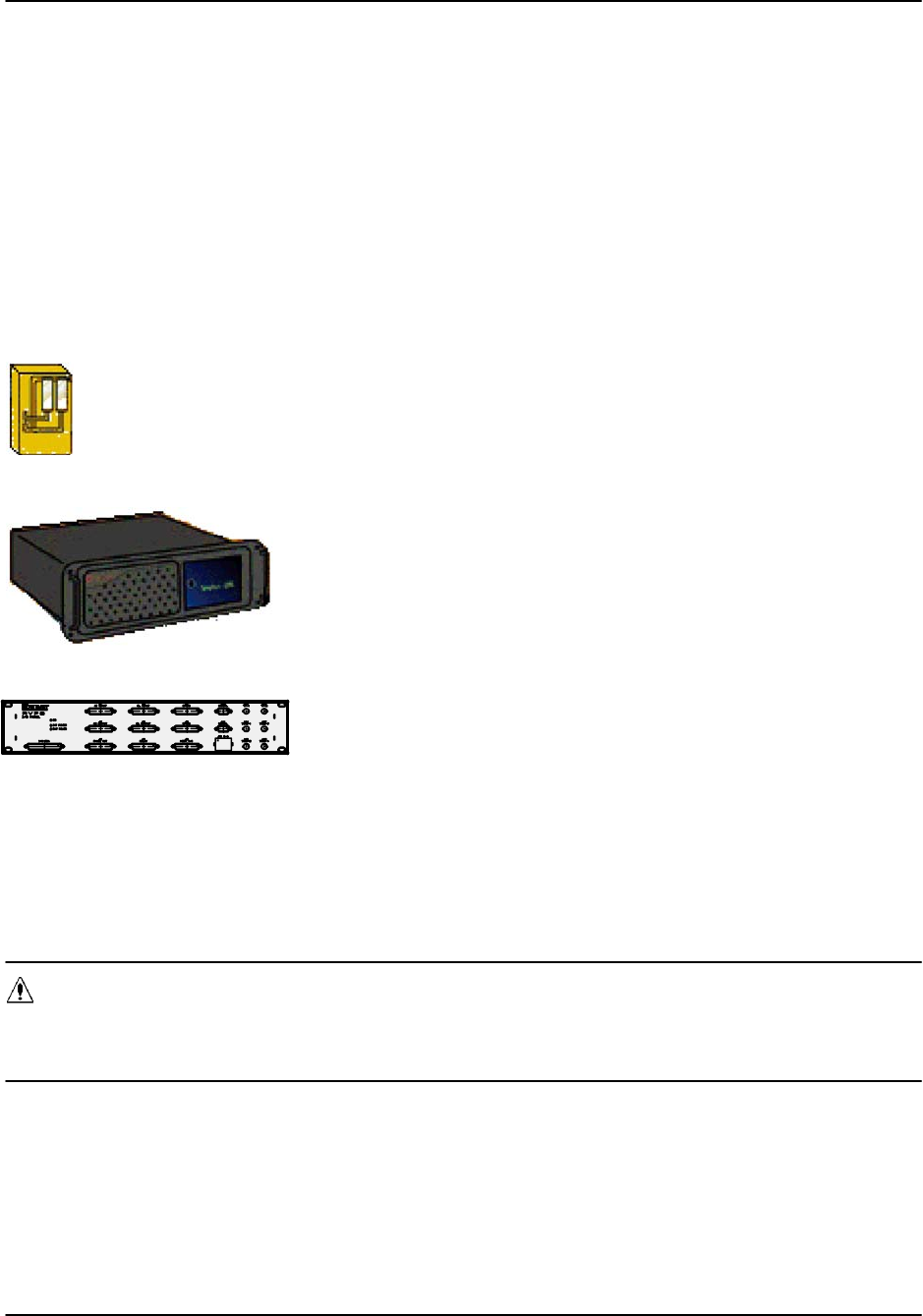
Hardware Installation
RVP8 User’s Manual
May 2003
2–1
2. Hardware Installation
2.1 Overview and Input Power Requirements
This chapter describes how to install the RVP8 hardware. Topics include mechanical installation
and siting, electrical specifications of the interface signals, system-level considerations and the
standard connector panel that is provided.
There are three major modules supplied with the RVP8. These are:
IFD (IF Digitizer) Typically mounted in the radar receiver cabinet.
Input Power 47–63 Hz 100–240 VAC Auto-ranging
Main Chassis Usually mounted in 19” EIA rack.
Input Power 60/50 Hz 115/230 VAC Manual Switches
I/O-62 Connector Panel
Usually mounted in 19” EIA rack within 2 m of Main Chassis
Much of the RVP8 I/O is configured via software. This makes the unit very flexible. Also, since
there is virtually no custom wiring, it is very easy to insert spare modules and circuit cards. The
software configuration of the I/O is described in Appendix A.
This section, in conjunction with Appendix B, describes the physical installation of the
hardware.
WARNING: The Main Chassis redundant power supplies are NOT auto-ranging
like the IFD. These are factory configured for the expected voltage, but should
be VERIFIED by the customer before power is applied to the system.

Hardware Installation
RVP8 User’s Manual
May 2003
2–2
2.2 IFD IF Digitizer Module Installation
2.2.1 IFD Introduction
The IFD IF digitizer is housed in an electrically sealed solid metal enclosure to achieve good
immunity to external electrical noise. The internal circuitry has been designed to minimize the
number of digital components, and it is carefully grounded and shielded to make the cleanest
possible samples of the input IF signal. The unit is cooled by direct conduction of heat through
the metal chassis; there are no openings required for airflow.
The IFD replaces all of the IF receiver components that are found in a traditional analog receiver
system, i.e.,
SBand Pass Filters
SLOG Receiver
SAFC Circuit
SAGC or IAGC circuit
SQuad Phase Detector
SCOHO (on magnetron systems)
SLine drivers for base band video
Indeed, one of the most time consuming parts of an upgrade is often the removal of old
components. Many customers choose to simply bypass them and leave them in place. In some
cases there will be other receiver modifications required to match the IFD signal input
specifications. For example, IF attenuators or an IF amplifier are sometimes required.
If you are doing an upgrade of an older system, you might want to consider
purchase of a new STALO which can make significant improvements in Doppler
performance.
You should carefully document and red-line your system schematics to reflect any changes to the
receiver.

Hardware Installation
RVP8 User’s Manual
May 2003
2–3
2.2.2 IFD Revision History
There have been several versions and evolutions of the IFD. Table 2–1 summarizes the
differences among all of the versions that have been manufactured so far. This document covers
only the 14–bit units although the previous generation 12–bit units are compatible with the
RVP8 as well.
Table 2–1: Differences Among Versions of the IFD
Rev.B Rev.C Rev.D
A/D Chip Analog Devices AD9042, 12–Bits AD6644, 14–Bits
Input Signal
Level A/D saturation at +4.5dBm A/D saturation at +6.0dBm
A/D Noise
Density –76dBm/MHz –82dBm/MHz
Dynamic
Range 93dB at 0.5MHz 101dB at 0.5MHz
Ext-Clock No Yes (shared with AFC connector)
Noise
Generator None. The A/D dither power must be supplied from
wideband thermal noise in the RF/IF chain.
Built-in noise source supplies A/D
dither power in the 200–900KHz
range.
Power Supplies +5V, +12V, –12V +5V Only. +12/15V required only for
analog AFC output
Jumpers
(Table 2–5) None AFC/Clock I/O AFC/Clock I/O
Dither and Config Selections
Uplink
Protocols AFC-16 AFC-16 & PLL-16 Supports full set of protocols defined
in Section 2.5.1
First
Production March 1997 April 1998 December 2000

Hardware Installation
RVP8 User’s Manual
May 2003
2–4
2.2.3 IFD Power, Size and Physical Mounting Considerations
The IFD is a compact sealed module with dimensions 23.6 x 10.9 x 3.0 cm. (9.3 x 4.3 x 1.2 in).
The unit is designed to be mounted on edge such that the 23.6 x 3.0 cm. surface is flush on the
back of the receiver cabinet with 10.9 cm. protrusion into the cabinet. The unit is typically
placed where a traditional LOG receiver would be installed. The IFD is cooled by direct
conduction through its metal enclosure. It should be positioned so that air can freely convect
around it, or bolted to a larger surface that will conduct the heat away.
The power supply module is separate and can be mounted nearby in the radar cabinet, or it can
be attached directly to the IFD using a special mounting bracket. The power supply and bracket
will add 3.3 cm. (1.3 in) of overall width to the receiver module.
The power supply is a low noise, low ripple, switching unit; the input voltage range is 100–240
VAC 47–63 Hz, autoranging. The IFD has an internal 3-stage power supply input filter to
minimize interference from the power cable. Nonetheless, it is still good practice to insure that
the four supply wires (+5V, –12V, +12V, and Ground) be kept short and twisted together. A
ferrite choke around the supply wires near the terminal strip is also recommended.
Important: The inductive filtering components inside the IFD introduce a slight
voltage drop in the +5V supply. To produce the correct internal voltage, the
supply voltage measured at the external terminal block should be 5.23V for
Rev.D boards, and 5.17V for Rev.C and earlier boards.
Mounting space should also be reserved for the external analog anti-alias filters. These filters
can be mounted in the radar cabinet itself, or they can be attached directly to the IFD on the
opposite side of the power supply. The filters and mounting bracket will add 2.0 cm. (0.8 in) of
overall width.

Hardware Installation
RVP8 User’s Manual
May 2003
2–5
2.2.4 IFD I/O Summary
The connectors on the IFD are labelled as shown in the table below. The connections to the IFD
are as follows:
Table 2–2: IFD I/O Connections
IFD I/O Summary
Connector
Label
Style Description Reference
J1
IFĆIN
SMA IF signal from LNA/mixer; via an antiĆaliasing filter
centered at IF (supplied by SIGMET). 50W, + 6.5 dBm
max
2.2.6
2.2.7
2.2.8
2.2.9
J2
BURST
(COHO)
SMA IF Tx sample from waveguide tap and mixer; via an
antiĆaliasing filter centered at IF (supplied by SIGĆ
MET). 50W, +6.5 dBm max
2.2.6
J3
AFC
(CLK)
SMA AFC output (+-10V) or reference clock input for coĆ
herent systems (2-60 MHz -10 to 0 dBm). The funcĆ
tion of the connector is controlled by jumper selecĆ
tion within the IFD.
2.2.10 AFC
2.2.11 CLK
J4
UPLINK
SMA/BNC Connects to the RVP8 Main Chassis by 75 Ohm
shielded cable. The connector is SMA with an SMA/
BNC adapter provided.
2.2.12
J5
FIBERĆOUT
ST 62.5/125 micron multimode optical cable terminated
in type ST connectors. IFD cam be located up to
100m from the RVP8 Main Chassis.
2.2.12
Since they share the same connector, the case of analog AFC output and reference clock input is
not supported. However, this is a very rare occurrence since an analog AFC output is used for
magnetron systems and a reference clock input is typically used for fully coherent TWT and
Klystron systems.

Hardware Installation
RVP8 User’s Manual
May 2003
2–6
2.2.5 IFD Adjustments and Test/Status Indicators
The IFD is packaged in a tight metal enclosure for maximum noise immunity. The only
adjustments on the module are the internal gain and offset pots that adjust the AFC analog
output. Two switches on the unit provide standalone test features to verify the proper functioning
of the IFD and to assist with setting the voltage span of the AFC DAC.
Table 2–3: IFD Toggle Switch Settings
SW1 SW2 Function
A A AFC Test Low Voltage
A B AFC Test Midpoint Voltage
A C AFC Test High Voltage
B A Swap Burst and IF Input Signals
B B Normal Operation (also labeled as “run”)
B C Reserved (fiber test pattern)
C A Reserved
C B Reserved (fiber test pattern)
C C Reserved (fiber test pattern)
Two LEDs provide information on the status of the module and the status of the communication
to the RVP8 (fiber channel and uplink).
Table 2–4: IFD LED Indicator Interpretations
Red (Uplink) Green (Ready) Meaning
Blink Blink Reset sequence (powerup, or from uplink)
Blink Off Uplink is dead (no signal from RVP8/Rx)
On Off Uplink is alive, but downlink is dead
On On Normal Operation (IFD and Main are both okay)

Hardware Installation
RVP8 User’s Manual
May 2003
2–7
The internal jumper settings are summarized in the following table. Please also refer to Sections
2.2.10 and 2.2.11 for more information on setting up the AFC or External Clock options.
Table 2–5: IFD Internal Jumper Settings
Rev.B Rev.C Rev.D
JP1 N/A AB: AFC Voltage Output
BC/Open: External Clock Input 50W/Open Termination
JP2 N/A Reserved
JP3 N/A BC: External Clock
Open: AFC Voltage Output
JP4 N/A AB: Dither Applied to Burst Input
BC: No Dither on Burst

Hardware Installation
RVP8 User’s Manual
May 2003
2–8
2.2.6 IFD Input A/D Saturation Levels
There are two analog signals that must be supplied to the IFD:
SIF receiver signal
SIF Tx Sample (Burst Pulse) for magnetron, or COHO reference for klystron.
Both of these inputs are on SMA connectors. The IF signal should be driven by the front-end
mixer/LNA/IF-Amp. components, similar to the way that a LOG receiver would normally be
installed. The magnetron burst pulse or klystron COHO reference is also derived in the same
manner as a traditional analog receiver.
Note: Even for fully coherent Klystron and TWT systems, SIGMET
recommends the use of an actual IF Tx sample. If this is not possible, then the
COHO is used instead. If there is phase modulation, then the phase-shifted
COHO should be input.
The A/D input saturation level for both the IF-Input and Burst-Input is +6 dBm (4.5 dBm for
Rev.C or earlier). In almost all installations an external anti-alias filter is installed on both of
these inputs. These filters (if supplied by SIGMET) are mounted externally on one side of the
IFD, and have an insertion loss of approximately 1–2dB. Thus, the input saturation level will be
+8dBm measured at the filter inputs.
For the burst pulse or COHO reference it is important not to exceed the A/D saturation level.
This reference signal should be strong enough so that most of the bits in the A/D converter are
used effectively, but it should also allow a few deciBels below the saturation level for safety.
The recommended power level is in the range –12 to +1 dBm, measured as described in section
E.14. This is important for making a precise phase measurement on each pulse.
In contrast, for the IF receiver input it is permissible (in fact desirable) to occasionally exceed
the A/D input saturation level at the strongest targets. The RVP8 employs a statistical
linearization algorithm to derive correct power levels from targets that are as much as 6dB above
saturation. The actual IF signal level should be established by weak-signal and noise
considerations (see below), rather than by working backwards from the saturation level.

Hardware Installation
RVP8 User’s Manual
May 2003
2–9
2.2.7 IF Bandwidth and Dynamic Range
The RVP8 performs best with a wide bandwidth IF input signal. This is because a wideband
signal can be made free of phase distortions within the (relatively narrow) matched passband of
the received signal. The RVP8 uses an external analog anti-aliasing filter at each of its IF and
Burst inputs. The purpose of these filters is to block frequencies that would otherwise alias into
the matched filter passband. The anti-alias filters have a nominal passband width of 14 MHz
centered at 30MHz, i.e. from 23MHz to 37MHz. This is the recommended operating bandwidth
for the IF signal, although the RVP8 will still work successfully with lesser IF bandwidth.
At the 36MHz sampling rate the quantization noise introduced by LSB uncertainties is spread
over an 18MHz bandwidth. For an ideal 14-bit A/D converter that saturates at +6dBm the
effective quantization noise level would be:
)6dBm *20log(214)*10log(18MHz
1MHz )+*90 dBm
MHz
If samples from this ideal converter were processed with a digital filter having a bandwidth of
1MHz, then an input signal at –90dBm would have a signal-to-noise ratio of 0dB. A narrower
FIR passband (corresponding to a longer transmitted pulse) would decrease the quantization
noise even further, so that 0dB SNR would be achieved at even lower input power.
In practice, the 14-bit A/D converter used inside the IFD does not behave quite this well. The
Analog Devices AD6644 chip has been measured to have a wideband SNR of 76dB, i.e., 8dB
less than the 84dB range expected for an ideal converter. The above calculation for noise
density thus becomes:
)6dBm *76dB *10log(18MHz
1MHz )+*82 dBm
MHz
Indeed, the RVP8’s receiver power monitor described in Section 4.6 will show a filtered power
level of approximately –82dBm when the FIR bandwidth is 1MHz and the IFD inputs are
terminated in 50–Ohms.
The inverse correspondence between filter bandwidth and the 0dB SNR signal level leads to an
interesting and useful property of wideband digital receivers: they can operate over a dynamic
range that is much greater than the inherent SNR of their A/D converter would imply. If this
particular A/D chip were performing direct conversion at “base band” it would have a dynamic
range of only 76dB. However, by utilizing the extra bandwidth of the converter, the RVP8 is
able to extend the dynamic range to approximately 100dB.
To understand this, begin with the 88dB interval between the converter’s +6dBm saturation level
and the –82dBm 0dB SNR level at 1MHz bandwidth. Add to this:
S6dB for the statistical linearization that is performed on signals that exceed the
saturation level. The RVP8 can recover signal power accurately even when the
A/D converter is driven beyond saturation. Velocity data will also be valid, but
spectral width may be overestimated.
S4dB for usable dynamic range below the 0dB SNR level. In practice, a coherent
signal at –4dB SNR can easily be measured when 25 or more pulses are used.
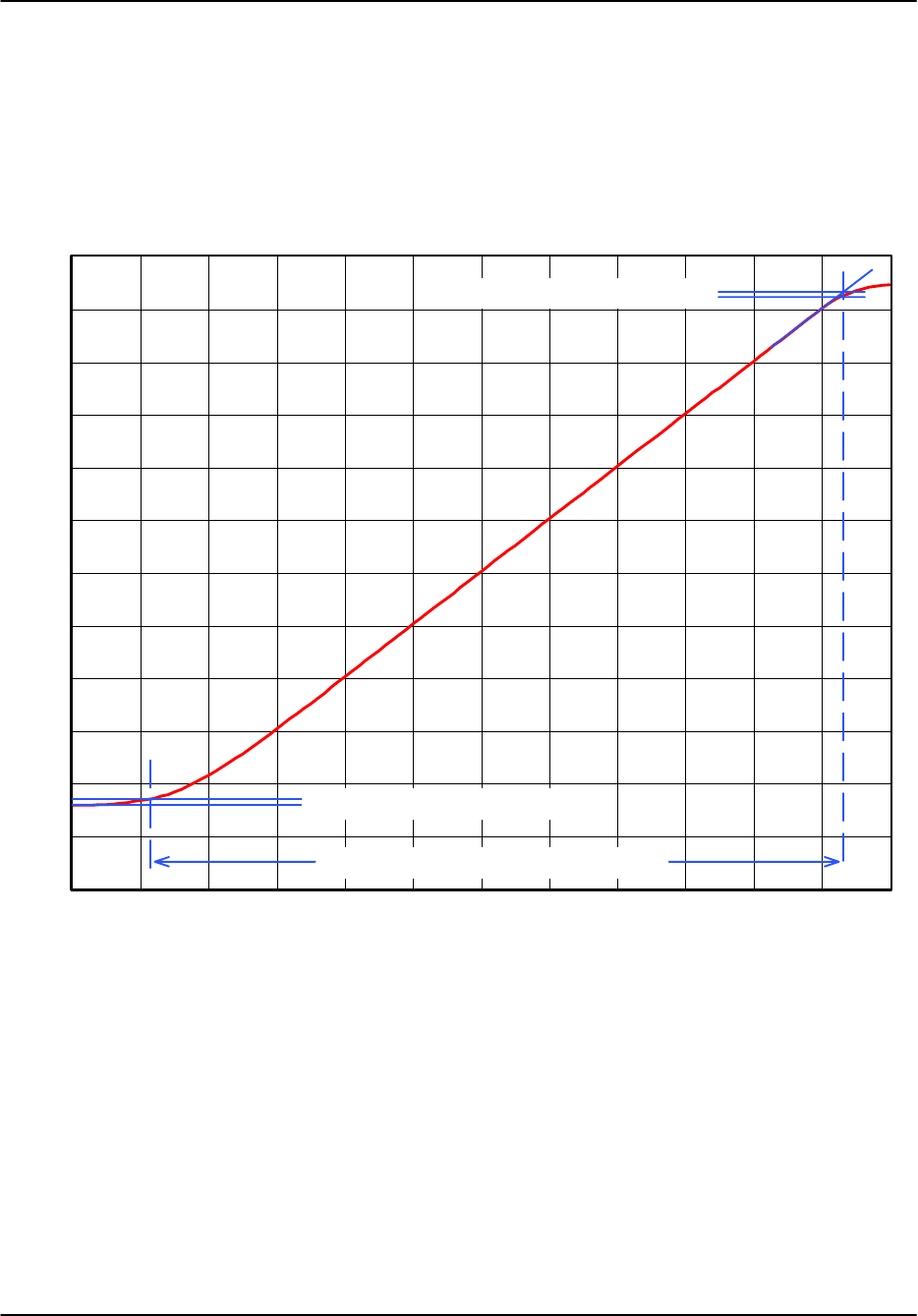
Hardware Installation
RVP8 User’s Manual
May 2003
2–10
Thus, the overall dynamic range at 1MHz bandwidth (approx. 1 msec transmit pulse) is 88+6+4
= 98dB. For a 0.5 msec pulse the dynamic range would be reduced to 95dB; but it would
increase to 101dB for a 2.0 msec pulse. An actual calibration curve demonstrating this
performance is shown in Figure 2–1, for which the RVP8’s digital bandwidth was set to
0.53MHz and external signal generator steps of 1dB were used over the full operating range.
Figure 2–1: Calibration Plot for a Stand-alone 14-Bit IFD
–100
–90
–80
–70
–60
–50
–40
–30
–20
–10
0
10
20
–100 –90 –80 –70 –60 –50 –40 –30 –20 –10 0 10 20
1-dB Detection Threshold
Input Power in dBm Measured at IFD IF-Input
1-dB Compression Point
Overall Dynamic Range of 101dB
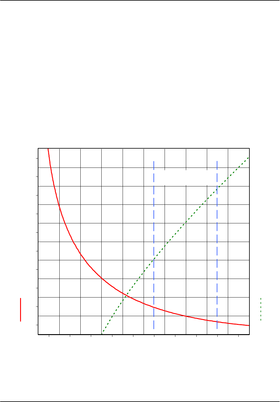
Hardware Installation
RVP8 User’s Manual
May 2003
2–11
2.2.8 IF Gain and System Performance
The previous discussion was concerned with measuring the dynamic range of a stand-alone IFD.
We will now examine how the unit performs in the context of a complete radar receiver. We
assume that an LNA/Mixer has already been selected that offers an appropriate balance between
price and noise figure. Having chosen these front-end components, the only parameter that
remains to be determined is the total RF/IF gain between the antenna waveguide and the IFD.
Assume that the thermal noise (kT) of the system is –114dBm/MHz, and that the noise figure of
the LNA/Mixer is 2dB. We wish to bring this –112dBm/MHz noise level up into the working
range of the IFD so that the received echoes can be optimally processed. However, in trying to
select the required gain, we realize that we must make a tradeoff between preserving the receiver
sensitivity that has been established by the LNA, and preserving the overall dynamic range of
the IFD. This is the exact same tradeoff that is made in traditional multi-stage analog receiver
systems that include a wide dynamic range LOG receiver.
0
1
2
3
4
5
6
7
8
9
10
012345678910
Reduction of Receiver Sensitivity (dB)
Reduction of IFD Dynamic Range (dB)
Figure 2–2: Tradeoff Between Dynamic Range and Sensitivity
Recommended
Operating Region
Power Ratio R = 10log10( NLNA / NIFD )
The solid red curve in Figure 2–2 shows that these two variables interact in a symmetric manner,
so that any operating point (x,y) is always matched by a dual operating point at (y,x). To
understand the construction of this plot, let NIFD represent the stand-alone (terminated input)

Hardware Installation
RVP8 User’s Manual
May 2003
2–12
noise power of the IFD over some bandwidth. Similarly, let NLNA represent the LNA/Mixer
thermal noise power over that same bandwidth, and after amplification by all RF and IF stages.
Note that NIFD is primarily due to the quantization noise that is introduced by the A/D converter,
whereas NLNA has its origins in the fundamental thermal noise of the receiving system. The
reduction of receiver sensitivity is the amount by which the LNA thermal noise is increased over
the original level established by the front-end components:
DSensitivity +10 log10(NLNA )NIFD )*10 log10(NLNA )+10 log10ǒ1)NIFD
NLNAǓ
Likewise, the reduction of RVP8 dynamic range is the amount by which the IFD quantization
noise is increased over its stand-alone value:
DDynamicRange +10 log10(NLNA )NIFD )*10 log10(NIFD )+10 log10ǒ1)NLNA
NIFDǓ
Note that both of these quantities depend only on the ratio of the two powers; hence, the two
equations define a parametric relationship in the dimensionless variable R+(NLNA ńNIFD ).
Figure 2–2 was created by sweeping the value of R from 1/9 to 9. The solid red curve shows the
locus of ( DDynamicRange,DSensitivity ) points, and the dashed green curve shows R itself
(expressed in dB) as a function of DDynamicRange. For example, when the LNA noise power
is equal to the IFD noise power, R is 1.0 (0dB) and there will be a 3dB reduction in both
sensitivity and dynamic range.
The recommended operating region is the portion of the curve that limits the loss of sensitivity
to between 1.4dB and 0.65dB. The attendant loss of dynamic range will fall between 5.5dB and
8.5dB respectively. Each axis of the plot has an important physical interpretation within the
radar system.
SThe horizontal axis is equivalent to the increase in the RVP8’s report of filtered
power when the IF-Input coax cable is connected versus disconnected. This is an
easy quantity to measure, and thus provides a simple way to check the overall
gain of the LNA/Mixer/IF components.
SThe vertical axis is equivalent to a worsening of the LNA/Mixer noise figure.
This can also be interpreted as the amount of transmit power that is, in some
sense, “wasted” when observing very weak echoes. If you have installed an
expensive LNA with a very low noise figure, then you will want to pick an
operating point that makes the most of preserving that investment.
Figure 2–2 can be used to calculate the net gain that is required by the front-end components,
and to predict the final system performance:
1. Choose an operating point that balances your need for sensitivity versus dynamic
range. For this example, we will allow a 1dB loss of sensitivity from the
theoretical limit of the LNA/Mixer, and will assume a bandwidth of 0.5MHz.
2. For a 1dB loss of sensitivity, the DDynamicRange is first determined from the
solid red curve as 7dB. The required noise ratio R is then read vertically on the
dashed green curve as 6.1dB.

Hardware Installation
RVP8 User’s Manual
May 2003
2–13
3. Thus, the RF/IF gain must bring the front-end thermal noise at –112dBm/MHz up
to a level that is 6.1dB higher than the IFD noise density of –82dBm/MHz. The
gain is therefore (–82dBm/MHz + 6dB) – (–112dBm/MHz) = 36dB. Note that
this gain does not depend on bandwidth, and therefore will be correct for all
pulsewidth/bandwidth combinations.
4. The dynamic range for the complete system at 0.5MHz bandwidth may now be
calculated as 101dB – 7dB = 94dB.
5. After assembling all of the RF and IF components we can check whether we
achieved the correct gain by verifying a 7dB rise (independent of bandwidth) in
RVP8 filtered power when the IF-Input cable is connected versus disconnected.
Keep in mind when designing your RF and IF components that the final amplifier driving the
IFD must be capable of driving up to +14dBm, so that signals above saturation can be correctly
measured.
2.2.9 Choice of Intermediate Frequency
The RVP8 does not assume any particular relationship between the A/D sample clock and the
receiver’s intermediate frequency. You may operate at any IF that is at least 2MHz away from
any multiple of half the 35.9751MHz sampling rate (nominally 18, 36, 54, 72 MHz). The valid
frequency bands are thus:
6-16MHz, 20-34 MHz, 38-52 MHz, 56-70 MHz
There are many reasons for staying clear of the Nyquist frequency multiples. Most of these
considerations would apply to all types of digital processors, and are not specific to the RVP8.
As an example of what can go wrong at the Nyquist frequencies, suppose that an intermediate
frequency of 35MHz was used. This is only 1MHz away from the (approximately) 36MHz
sampling rate. The external anti-alias filter must now be designed much more carefully since a
spurious input signal at 37MHz would be aliased into the valid 35MHz band. If the valid signal
bandwidth were 2MHz, then the anti-alias filter would have the difficult task of passing
34–36MHz free of distortion while rejecting everything above 36MHz. The filter’s transition
zone would have to be very sharp, and this is difficult to achieve.
Another problem that would arise with a 35MHz IF on a magnetron system would be the RVP8’s
computation of AFC. If the processor can not distinguish 37MHz from 35MHz, then it can not
tell the difference between the STALO being correctly on frequency, versus being 2MHz too
high. The symmetric AFC tracking range would be reduced to the very small interval
34–36MHz.
For similar reasons (i.e., transition band width), the digital FIR filter itself also becomes difficult
to design when its passband is near a Nyquist multiple. But there is an additional constraint that
the digital filter should have a very large attenuation at DC. This is so that fixed offsets in the
A/D converter do not propagate into the synthesized “I” and “Q” data. Since 36MHz is aliased
into DC, we are left with the contradictory requirements of a zero very close to the edge of the
filter’s passband.

Hardware Installation
RVP8 User’s Manual
May 2003
2–14
2.2.10 IFD Analog AFC Output Voltage (Optional)
An analog AFC voltage is produced by a 16-bit DAC whose output limits are –10V to +10V.
Gain and Offset potentiometers on the IFD module set the actual operating span within these
limits. Use the switch settings described below to force the low, center, and high voltages to be
output, and then adjust the two potentiometers so that the desired voltage span is achieved. The
Offset adjustment is independent of the Gain adjustment. Hence, a good strategy is to first set
the switches for the midpoint voltage, and adjust the Offset potentiometer so that the center IF
frequency is produced by the STALO mixer. Then, adjust the Gain potentiometer for the desired
tuning range around that center point. The midpoint voltage will not change as you vary the
overall span.
AFC voltage output is always enabled on Rev.B (and earlier) IFD boards. On Rev.C (and later)
boards, the AFC function shares the same connector with the optional reference clock input (See
Section 2.2.11). AFC can be enabled on a Rev.C board as follows:
SRemove U14
SInstall U11, U12, U13
SSet JP1 to its AB position, which is also labeled “AFC”.
SInstall fixed frequency stable 35.975MHz oscillator at U5.
The instructions are similar for a Rev.D board except that you do not need to remove U14, and
you must check that no jumper has been placed on JP3/BC.
Additional information about using AFC can be found in Sections 2.4, 3.3.6, and 5.1.2.

Hardware Installation
RVP8 User’s Manual
May 2003
2–15
2.2.11 IFD Reference Clock Input (Optional)
When the RVP8 is used in a klystron system, or in any type of synchronous radar, the radar
COHO is supplied to the IFD so that the processor can digitally lock to it. The COHO phase is
measured at the beginning of each transmitted pulse, and is used to lock the subsequent (I,Q)
data for that pulse. The COHO phase is measured relative to the IFD’s own internal stable
sampling clock, which is nominally 35.975MHz. The internal sampling clock itself is not
affected by the application of the COHO. Rather, A/D samples of the COHO are obtained at the
fixed sampling rate, and the (I,Q) data are digitally locked downstream in the RVP8 IF-to-I/Q
processing chain (see Figure 1–3). The procedure is identical to the manner in which phase is
recovered in a magnetron system, except that the COHO signal is used in place of a sample of
the transmit burst.
There are two special concerns that may come up when the RVP8 is used in the above manner
within a synchronous radar system. Both concerns are the result of the IFD’s sampling clock
being asynchronous with the radar system clock.
SRVP8 Generates the Radar Trigger
The trigger signals supplied by the RVP8 are synchronous with the IFD data
sampling clock. This is accomplished by a clock recovery PLL on the RVP8/Rx
that provides on-board timing which is identical to the sampling clock in the IFD.
However, since the IFD sampling clock is asynchronous with the radar clock(s),
the RVP8 trigger outputs are likewise asynchronous. The result is that each
transmitted pulse envelope will be triggered independently of the COHO phase.
The transmitted pulse is still synchronous –– but the precise alignment of the
amplitude modulated envelope will vary.
In almost all cases, the exact placement of the transmitter’s amplitude envelope
does not affect the overall system stability, nor the ability of the RVP8 to reject
ground clutter and to process multi-mode return signals. For this reason, a
synchronous radar system that is triggered using the RVP8 triggers will still
perform optimally using the standard digital COHO locking techniques. In spite
of this, however, some system designers may still prefer that the amplitude
envelope itself be locked to the COHO.
SRVP8 Receives the Existing Radar Trigger
When an external trigger is supplied to the RVP8, the processor synchronizes its
internal range bin selection circuitry to that external trigger. The placement of the
range bins themselves, however, is always synchronous with the IFD’s
35.975MHz acquisition clock. The result is that 27.8ns of jitter is introduced in
the placement of the RVP8’s range bins relative to the transmitted pulse itself.
The effect of this synchronization jitter is that targets appear to be fluctuating in
range by approximately 4.2 meters. Although this is small relative to the range
bin spacing itself, and thus does not affect the range accuracy of the data, the
effect on overall system stability is more severe. Using both numerical modeling
and actual field measurements, we have found that sub-clutter visibility of a msec
pulse may be limited to approximately 43dB as a result of this 27.8ns range jitter.

Hardware Installation
RVP8 User’s Manual
May 2003
2–16
This falls quite short of the usual expectations of a synchronous radar system in
which clutter rejection of 55–60dB should be attainable.
The solution to either of the above concerns is to provide some means for the IFD’s internal
sampling clock to be phase locked to the radar system. If the RVP8 provides the radar triggers,
then those triggers would become synchronous with the radar COHO; and if the RVP8 receives
an external trigger, then its range bin clock would be synchronous with that external trigger, and
thus, there will be no synchronization jitter in the range bins.
The Rev. C version of the IFD offers the option of locking its sampling clock to an external
system clock reference. This results in an RVP8 that is fully synchronous with the existing radar
timing. Rather than being derived from a fixed-frequency oscillator, the phase locked IFD
sampling clock is driven by a custom Voltage-Controlled-Crystal-Oscillator (VCXO). This
oscillator can have a center frequency in the 33.5 to 39.5MHz range, which is any rational
multiple P/Q of twice the input reference frequency, where P and Q are integers between 1 and
128 (See also, Section 3.3.6). The tuning range of the VCXO is purposely kept very narrow (to
improve the clock stability), and is restricted to approximately +/–50ppm. Thus, the input
reference clock frequency must be precisely specified so as to stay within these limits.
The reference clock input frequency range is 2–60 MHz, and the input power level level must be
between –10 and 0dBm. Use the following configuration to allow a Rev.C IFD to lock its
sampling clock to an external reference:
SInstall U14
SRemove U11, U12, U13
SSet JP1 to its BC position to terminate the reference input in 50W, or leave the
jumper open to achieve a high-impedance input (approx. 5KW).
SInstall custom Voltage-Controlled-Crystal-Oscillator (VCXO) at U5. Please
contact SIGMET for assistance in specifying this device.
For a Rev.D board the instructions are similar except that you do not need to remove any
components, and should place a jumper on JP3/BC
Warning: As noted in the previous section, for Rev.C boards U14 Must Be
Removed whenever the VCXO phase lock mode is not being used, i.e., when the
normal free-running crystal is installed.

Hardware Installation
RVP8 User’s Manual
May 2003
2–17
2.2.12 Coax Uplink and Fiber Downlink
There are two cable links between the IFD module and the RVP8 Main Chassis:
SCopper coax cable uplink from the RVP8/Rx board. Provides timing information
for the burst pulse window, and 16-bit data for setting the AFC output level.
SOptical fiber downlink to the RVP8/Rx board. The receiver and burst pulse data
samples are encoded into a 540MHz serial stream.
The uplink input from the RVP8 is an SMA input from a 75W shielded cable (e.g., RG59 cable)..
This cable is electrically isolated from the receiver’s ground (40KW isolation) so that noise
picked up by the cable will not be coupled into the receiver circuitry. The downlink uses a
62.5/125 micron multimode optical cable terminated in type ST connectors. The coax and fiber
cables can be any length up to 100 meters apiece. The RVP8 measures the round trip cable
delays each time it boots up, and then uses that information to correct for range and timing
offsets due to cable length.
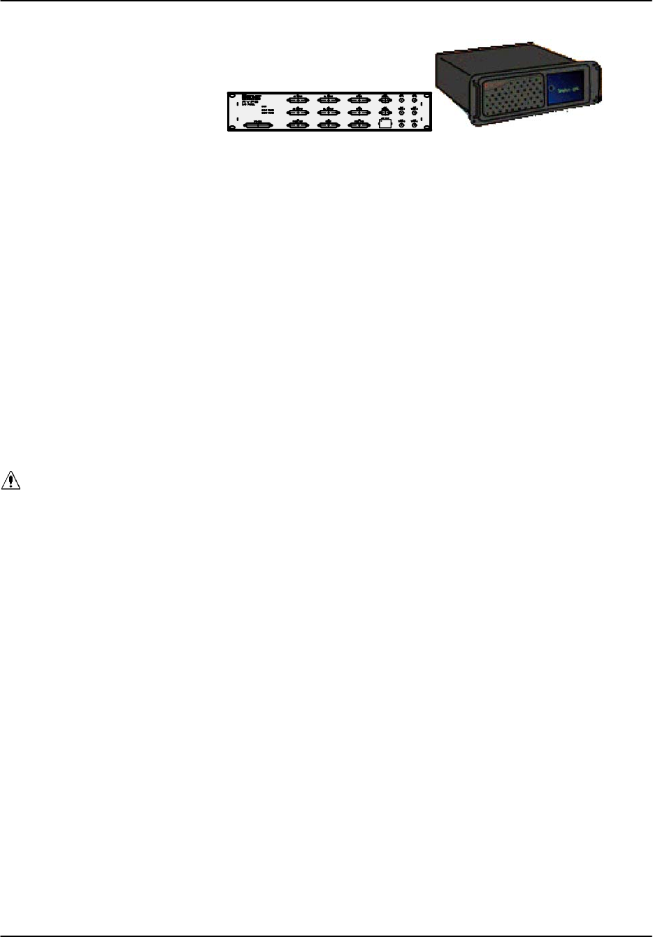
Hardware Installation
RVP8 User’s Manual
May 2003
2–18
2.3 RVP8 Chassis
2.3.1 RVP8 Chassis Overview
The RVP8 main chassis can assume a variety of forms depending on the customer requirements.
Appendix B describes a standard SIGMET system. A typical unit supplied by SIGMET
contains at least the following:
SA dual CPU on either motherboard or SBC in a passive PCI backplane
SRVP8/Rx Card
SI/O-62 Card and Connector Panel
The system is also shipped with an integrated hard disk drive (HDD), 1.44 MB floppy (FDD)
and CDRW unit. Note some installations may use a flash disk drive instead of an HDD. There is
an LED display panel on the front of the chassis that is used to report system status.
2.3.2 Power Requirements, Size and Physical Mounting
WARNING: The Main Chassis redundant power supplies are NOT auto-ranging
like the IFD. These are factory configured for the expected voltage, but should
be VERIFIED by the customer before power is applied to the system.
There a three redundant power supplies
The standard SIGMET chassis is a 19” EIA 4U rackmount unit, 17” (43 cm) deep. The chassis is
usually mounted in a nearby equipment rack on rack slides (provided as standard). The
connector panel is usually mounted on either the front or the rear of the same rack. The standard
cable provided to connect the I/O-62 card in the main chassis to the connector panel is 6 feet
long (1.8 m) .
The power requirements are 100–240 VAC 47–63 Hz. The system is autoranging, i.e., there are
no switches or jumpers that must be set.
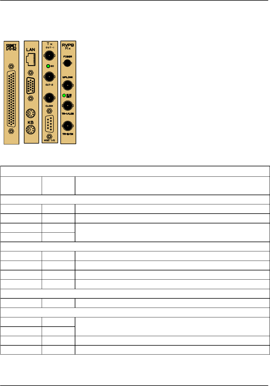
Hardware Installation
RVP8 User’s Manual
May 2003
2–19
2.3.3 Main Chassis Direct Connections
The direct connections to the RVP8 chassis are made either to the
back of the unit to PCI cards (e.g., left) or to the remote connector
panel. The direct connections are summarized in the table below.
Table 2–6: Direct Connections to RVP8 Main Chassis
IFD I/O Summary
Connector
Label
Style Description
Rx Card Connections
Uplink BNC COAX Uplink from IFD (75 shielded cable)
Fiber ST Fiberoptic downlink (orange cable)
Trig Out/In BNC Trigger outputs (12V, 75 ) or preĆtrigger input (1.8V threshold, 75 )
Trig Out BNC
SBC or Motherboard Connections
Network RJĆ45 10/100/1000 BaseT TCP/IP
Keyboard PS/2 Standard PC Keyboard
Mouse PS/2 Standard PC Mouse
Monitor VGA Standard PC Video Monitor
I/OĆ62 Connections
<no label> DBĆ62F SIGMETĆsupplied cable to IO62/CP remote panel
Optional Tx Card
IF Out 1 BNC Two independently synthesized IF output waveforms, up to +12dBm
into 50 8 75MHz
IF Out 2 BNC into 50 , 8Ć75MHz.
CLK BNC Optional input or output reference clock (50 )
Misc DBĆ9F Four optional RSĆ422 clocks or control lines
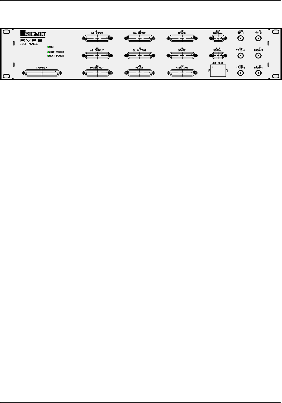
Hardware Installation
RVP8 User’s Manual
May 2003
2–20
2.3.4 Connector Panel I/O Connections
Most of the connections between the radar and the RVP8 are made using the RVP8 Connector
Panel which connects to the I/O-62 by 1.8m (6 foot) cable. The panel is usually mounted on the
front or the back of the same 19” EIA rack that contains the RVP8 chassis. The I/O-62 cable
may be plugged into either the front or the back of the connector panel to optimize the cable run.
The table in Section 1.8.5 provides a summary of the I/O for each connector. Detailed pin–out
assignments are given in Appendix C. Descriptions of the various signals are provided below.
J1 & J4- AZ/EL Input: TTL parallel angles
Thirty two TTL-Level input lines. These are sampled by the RVP8, and the bits accompany
each processed output ray (See PROC command, Section 6.7). The inputs can also be read
directly via the GPARM command (See Section 6.9). The RVP8 supports an antenna
synchronizing mode and inserts the AZ and EL start and stop angles into the ray header of each
radial (nominally 1 degree). Whenever antenna angle data are required, the processor reads the
azimuth lines up to ten times in a row (spaced by 0.5 msec) until two successive values compare
equal. This is done so that unsynchronized input data will be latched in a valid state. If after ten
retries the lines were never observed in a consistent state, then the last observed state is used.
Sampling for elevation is identical.
The format can be BCD or binary angle. Detailed pin assignments are given in Appendix B.
J2 & J5- AZ/EL Output: TTL parallel angles
These provide output of the AZ and EL angles in TTL BCD or binary angle format. Detailed pin
assignments are given in Appendix B. This feature could output the parallel angles to a separate
antenna controller for example.
J3- PHASE OUT: 8-bit RS422 phase shifter control output
Can be used as differential RS422 or as single–ended TTL. This is used to control a phase
shifter for coherent systems that use phase modulation, but do not have a Tx card. This is
typically used for legacy systems.
J6- RELAY: Control for external equipment
Often, external equipment in the radar will require relay control (e.g., power on, radiate on,
environmental systems, reset lines, slow polarization switch). This connector has connections for
3 internal relays that are on the connector panel itself. The maximum current through the relay
contacts is 0.5 A continuous. The switching load is 0.25 A and 100V, with the additional
constraint that the total power not exceed 4VA.

Hardware Installation
RVP8 User’s Manual
May 2003
2–21
If larger current and voltage loads are required, then the connector panel relays can be used to
switch external relays provided by the customer. Another alternative is to use the additional 4,
12V relay signals (up to 200mA) that are also supported on this connector.
Hazard: External relays must be equipped with proper diode protection against
back-EMF or damage to the I/O-62 and or the connector panel might result.
J7 SPARE: Configurable 20 lines of TTL I/O
This connector supports 20 lines of TTL each of which can be configured as either input or
output via the softplane.conf file.
J8 SPARE: Analog Inputs
10 differential analog inputs, up to ±20V max multiplexed into a single A/D convertor sampling
each at >1000 Hz. This can be used for monitoring environmental systems at the radar site.
J9- MISC: RS422 I/O, D/A and A/D
7 additional RS422 lines, each configurable to be either input or output, and 2 each dedicated
(non–multiplexed) A/D inputs (±580V with pot adjust) and D/A outputs (±10V). The RS422
lines are convenient for high-speed polarization switch control.
J10-11: RS232C I/O
These two connectors can be used for serial angle input. The most common format is the RCV01
format, although custom formats from antenna/pedestal manufacturers such as Orbit, Andrew
and Scientific Atlanta are also supported.
J12: S-D- AZ and EL synchro input
For systems that have synchros, the RVP8 can accept a direct synchro input from both AZ and
EL. The nominal voltage and frequency are 100V @ 60 Hz. S/D conversion is performed in the
I/O-62.
J13-14: TP1 & TP2: Programmable test point scope outputs
Am exciting feature of the RVP8 is the programmable test points. These are usually used to
connect to an oscilloscope. The user can then specify what is output to the test points in the form
of an analog voltage for display on the scope. Some examples are:
S“LOG” receiver power output (an old–time radar A–Scope)
SBurst pulse
SAnalog input monitor
The advantage of using the test points is that technicians can leave them permanently connected
to a rackmount oscilloscope and then select what is displayed. This saves time and reduces
cabling errors when test switching cables.

Hardware Installation
RVP8 User’s Manual
May 2003
2–22
J15-18: TRIG1-4- Output triggers
The waveforms appearing on the four trigger outputs are programmed by the user to meet the
radar’s exact timing needs. These correspond to the trigger generators TGEN1, TGEN2,
TGEN3 and TGEN4. More triggers can be configured on the “SPARE” connectors if they are
required. All lines may be setup and used independently and can contain, for example,
pre-trigger pulses, calibration gates, range strobes, scope triggers, etc. The triggers are driven at
+12V into 75W and can be independently-timed at rates between 50Hz and 20000Hz with better
than 0.02% accuracy. For dual-PRF velocity unfolding applications, the RVP8 trigger generator
must be used as opposed to an externally supplied pre-trigger (see next section).
The timing of the triggers is phase-locked to the sample clock in the IFD, which can be phase
locked to the COHO of a coherent system. For coherent systems that do not sample the actual
transmit pulse (for phase correction), this is recommended.
The trigger waveforms are configurable in software using the “mt” commands. This sets the
trigger timing, trigger sense (active high or active low pulse) and the minimum and maximum
PRF for each pulse width. See sections 3.3.4.
It is sometimes useful to dedicate one of the TRIG outputs to trigger an
oscilloscope.
J15: TRIG1- Selectable input pre-trigger
Users may supply the RVP8 with their own CMOS-Level pre-trigger for installations in which
adequate trigger control already exists. One of the connectors (typically TRIG1) may be
configured to accept an input pre-trigger. The trigger input uses CMOS levels (1.5V max low,
2.5V min high) for improved noise immunity. The trigger input may also be driven as high as
+100V or as low as –100V without damage. This makes it easier to connect to existing
high-voltage trigger distribution systems. The rising or falling edge of this external
“TRIGIN”signal is interpreted by the RVP8 as the pretrigger point; the actual pulsewidth of the
signal does not matter. The delay to range zero is configured via the TTY Setups. The other
trigger outputs are then synchronized to the input trigger. The synchronization jitter between the
user pretrigger and the other trigger outputs is less than 0.014 microseconds.
Trigger jitter can be improved in the case of coherent systems, by phase locking the IFD to the
same reference clock used to generate the external triggers (typically the COHO). This provides
approximately 10 dB of additional phase stability.
The RVP8’s response to a missing external trigger is that the processor will insert fake (software)
”triggers” at a rate of 250Hz whenever the trigger input is missing for more than 0.100 seconds.
These fake triggers will keep the RVP8’s internal code and external outputs running in spite of
the missing input (the data values will all be zero, and the ”no trigger” bit will be set in GPARM
immediate status word #1). Normal operation automatically resumes as soon as the external
trigger is restored.

Hardware Installation
RVP8 User’s Manual
May 2003
2–23
2.3.5 Power-Up Details (Alan)
Draft
WARNING: The Main Chassis redundant power supplies are NOT auto-ranging
like the IFD. These are factory configured for the expected voltage, but should
be VERIFIED by the customer before power is applied to the system.
Ideally, the RVP8 main chassis should be powered-up after or at the same time as the IFD. This
allows the diagnostic tests on the main board to run properly and exercise both components of
the system. If the main board is switched on first, then all of the IFD diagnostics will fail and
the RVP8 will be generally unusable, even if power were subsequently applied to the IFD.
Often the power sequencing order can not be controlled in detail, e.g., the IFD may be located in
a different cabinet or a different room from the main chassis. To help in these cases, the RVP8
performs a special power sequencing reboot whenever the IFD is turned on after the Main board
has already powered up. This special reboot will occur whenever a) the fiber signal was not
present at boot time, b) the last boot was not a power sequencing reboot, and c) the fiber signal
is detected for five continuous seconds. Thus, you may powerup your equipment in any order.
When the RVP8 is first powered up, it will always boot from the on-board ROM (nothing else
would be possible). but the ROM is also considered the most trusted source of code, and
therefore will also be used for all “hard” resets:
SExternal hardware RESET line (parallel interface reset)
SSCSI Bus reset sequence
SRVP8 “RESET” command with “Pwr” option selected
When the BOOT command has been used to install a new version of code, that new code will
persist across all of the following types of “soft” resets:
SAutoreset performed by the internal Watchdog
SAny type of reset invoked using the “*” local TTY command
SThe power sequencing reboot that occurs when the IFD is turned on after the
RVP8 board has already powered up.
SRVP8 “RESET” command with “Rst” or “Dig” options selected
A 32-bit CRC check is included in the RVP8’s boot ROM. This allows the entire ROM image to
be checked for internal consistency during the startup diagnostics, and during a reboot from the
host computer. An error bit is allocated in GPARM Output Word #12 to indicate a checksum
failure.
The CRC check is designed to accept ROMs that are programmed from either a 0x00 or 0xFF
blank state. If you are making your own ROMs from Intel Hex data files, you may use either
0x00 or 0xFF as the default value for ROM locations that are not explicitly defined by the file.
Note: SIGMET has support for third party RVP8 software developers who
would like to incorporate the BOOT command into their RVP8 driver.

Hardware Installation
RVP8 User’s Manual
May 2003
2–24
2.3.6 Socket Interface
The RVP8 as shipped is configured to listen on a network port. It is ready to interface to a host
computer via the network using a program called DspExport. It is also ready to run some
commands on the RVP8 itself. The RVP8 comes with some built–in SIGMET supplied utilities
such as setup, dspx and ascope. These utilities are described in the IRIS Utilities Manual.
Because the RVP8 can only have one program controlling it at a time, use of a local program
like dspx will block network access, and vice versa.
How DspExport Works
DspExport is a daemon program which is normally configured to run all the time. When it
receives a socket connection request it will establish an exclusive connection to the RVP8. If a
second connection request come in while the first is still active, it will fail, and return the
message ”Device allocated to another user”. To see if it is running on your RVP8, try typing
$ ps –aef | grep DspExport
During development, it can always be started up manually by typing “DspExport” at a shell
prompt. It can be started with the “–v” option for move detailed logging. It defaults to using
port 30740. If you wish to use another port, start it with an option such as “–port:12345”. The
command line option “–help” lists these options.
Source Examples
The source code for DspExport and for the dsp library is supplied on the RVP8 release cdrom.
This can be optionally installed as part of the upgrade procedure as discussed in section A.6.
You will find DspExport in ${IRIS_ROOT}utils/dsp, and you will find the dsp library in
${IRIS_ROOT}libs/dsp. In the library, you will find example code which talks to DspExport in
file OpenSocket.c, dsp_read.c and dsp_write.c. Search for the string “SOCKET”, and you can
see how the code differs between SCSI interface and socket interface.
Socket protocol
The socket interface basically supports all the “Host Computer Commands” in chapter 6. There
are a few layers of formatting on top of that. All messages going both ways consist at the lowest
level of an 8-character decimal ASCII number, followed by a block of data. The decimal
number indicates how many bytes follow. Generally, all data transfers are initiated by the host
computer by sending a block of data which consists of a command word followed by the “|”
character, followed by optional data.
It will respond to all commands with either an “Ack|” indicating acknowledgment that the
command was OK, or “Nak|” indicating that there was an error. For Nak, the reply will always
include a string indicating what the error was. For Ack there is optional data following.
On initial socket connection request DspExport will provide a response of either Nak indicating
the connection failed, and why, or Ack followed by some connection information. This Ack
string is in the form of name/value pairs, and will look something like:
Ack|CanCompress=1,Model=RVP8,Version=7.32

Hardware Installation
RVP8 User’s Manual
May 2003
2–25
Your program can choose to evaluate or ignore any of these keywords. “CanCompress=1”
indicates that the DspExport computer supports compression. The host computer can then
choose to use compression if it wants to. DspExport supports only the 5 commands discussed
individually below:
Read command (READ)
Example: “READ|100” means read 100 bytes from the RVP8. Since the RVP8 interface is a
16-bit word interface, these read sizes should always be even. It will always reply with a “Ack|”
followed by 100 bytes of binary data, or with a “Nak|”, in other words there can be no partial
reads.
Write command (WRIT)
Example: “WRIT|<data>” Where <data> is some binary data. This data is written to the RVP8.
Again, the data size should be even.
Read Status command (STAT)
Example: “STAT|” This reads the status bits back from the RVP8. This is a 1 bit value, set to 1
if the RVP8 has data available in its output buffer. It will return either “Ack|0”, or “Ack|1”, or a
“Nak”. This is the equivalent of the dspr_status() call in the dsp library.
Set Information command (INFO)
Example: “INFO|ByteOrder=LittleEndian,WillCompress=1,Version=7.32”. This command can
be used to inform RVP8’s DspExport about the host computer. Current options available are:
ByteOrder to inform DspExport of the byte order of the host computer. This is needed because
all the data read or written to/from the RVP8 is in 16-bit words. If the host computer has a
different byte order from the RVP8, DspExport will byte swap the data.
WillCompress to inform DspExport to use compression or not. Compression is only used if
both sides agree to use it. The host computer should only set this to 1 if it received a
“CanCompress” of 1 on initial connection. The only thing compressed is the data from normal
READ commands. If it is compressed, it will reply with the acknowledge compressed string of
“AkC”. The compression program is the zlib compress and uncompress. The uncompress
function requires that the caller know the expected uncompressed size. This is true for RVP8
reads, because the reader always specifies the read size.
Version, send the IRIS version.
Read data available command (RDAV)
Example: “RDAV|100|2” This means read up to 100 bytes of data from the RVP8 in individual
DMA transfers of 2 bytes each. Before each read, the status is checked to see if there is more
data available. If not, the read stops, and the number of bytes read is returned. This is merely a
performance enhancing command since the same feature is available by using the READ
command and the STAT command.

Hardware Installation
RVP8 User’s Manual
May 2003
2–26
Notes on migrating from the SCSI interface
Here are suggestions for customers who are converting an existing program which used a SCSI
interface to the RVP7 to the socket interface to the RVP8. First take a look at our source code
which handles either SCSI or socket. In OpenSocket.c you can see the code which replaces the
SCSI device open call. The SCSI inquiry command is replaced by reading the string returned
after the socket is opened. The SCSI read command is replaced by the “READ|..” command.
The SCSI modesense command is replaced by the “STAT|” command. The SCSI write
command is replaced by the ”WRIT|...” command. You should get your code working first
without using the RDAV command or using compression.
There is a significant difference between the RVP7 and RVP8 in regards to the FIFO reset
command. This is the RVP8 command 0x008C (see section 6.11). The RVP8 is unable to read
incoming commands if the output FIFO is entirely full. Therefore, if you put the RVP8 into
continuous output mode, then issue the FIFO reset command to return to interactive mode, it
may hang. To see how we have handled this problem, look in the source file DspResetFifo.c.
Basically we write the FIFO reset command, then loop waiting 1/10 of a second, then do a large
ReadAvailable command with DMA size 2 bytes. This continues until nothing is read back.
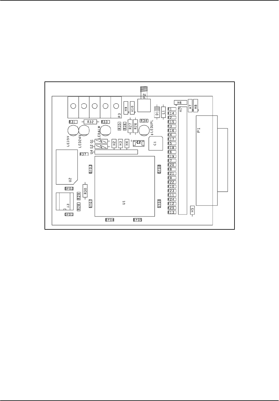
Hardware Installation
RVP8 User’s Manual
May 2003
2–27
2.4 Digital AFC Module (DAFC)
The DAFC is a small self-contained circuit board which can passively “eavesdrop” on the
RVP8’s serial uplink transmissions. Its purpose is to generate a set of digital AFC control lines
that could be applied, for example, to a custom STALO frequency synthesizer. A full size
(3”x3.75”) assembly diagram of the board is shown in Figure 2–3. It can be installed in the
radar system either as a bare board, or packaged into a small metal enclosure.
Figure 2–3: Assembly Diagram of the DAFC
SIGMET recommends that the DAFC board be used in new system designs whenever AFC is
required, as it offers these advantages over other methods of frequency control:
1) The use of a digital frequency synthesizer is superior to using analog AFC because
the stability of a synthesized STALO can be made much greater than that of a tunable
cavity oscillator. Also, noise on the AFC control voltage directly contributes to phase
noise in the received weather targets in analog AFC systems, so cabling of the control
signal can become tricky.
2) The RVP8 Connector Panel can also be made to output 8–bit AFC (TTL or
RS422). However, this is not in general recommended because of the potential for
noise on the cable which is typically run >2m into a radar cabinet. Using the DAFC
module is preferable because the board can be physically located very close to the
STALO. The length of the control cable and its susceptibility to noise and ground
loops are therefore reduced. Also, the DAFC board can supply up to 24 output
control lines, rather than just eight.
The digital output lines are made available as TTL levels on a 25-pin female “D” connector
(P1). There are 130W resistors (R1–R25) in series with each output line to help protect the
board against momentary application of non-TTL voltages on its external pins. However, these
resistors do impose a restriction on the input line configuration of the receiving device. To

Hardware Installation
RVP8 User’s Manual
May 2003
2–28
assure a valid TTL low level of 0.6V max. requires that the STALO inputs be pulled up to +5
with nothing less than (approx.) 1.2KW. Put another way, the low level input current of the
receiving device should not exceed 4.5mA. Most STALOs that we have seen use 5-20KW
pull-up resistors, so this should not be a problem.
All twenty five pins of the “D” connector are wired identically on the DAFC board, i.e., each pin
connects to one end of a 2-pin jumper (2x25 header H1), the other end of which connects to a
Programmable Logic Device (PLD) chip. The PLD lines can be configured either as inputs or
outputs, and this single chip handles all of the decoding and driving needs for the entire board.
For each “D” connector pin that is to be used as an AFC output or Fault Status input, you should
install the corresponding jumper to connect that pin through to the PLD, or use a wirewrap wire
if the pin must go to a different PLD line. The “D” connector pin numbers are printed next to
each of the jumper locations. Because of the ordering of the pins in the connector housing,
jumpers 1 through 13 are interleaved with jumpers 14 through 25.
The uplink protocol that the board should be expecting is selected by jumpers H3 and H4, as
summarized in Table 2–7. The first three table entries describe three fixed mappings of the
traditional AFC-16 uplink format onto various pins of the 25-pin “D” connector. One of these
choices must be used whenever the DAFC is interfaced to an RVP8 system whose uplink uses
the older style 16-bit AFC uplink format. In this case you will have to make most or all of the
pin assignments using wirewrap wire to connect each bit to its corresponding pin. This will be
somewhat tedious, but hopefully one of the three formats will be a reasonable starting point for
doing the wiring. By far the most preferable solution, however, is to use the Pinmap uplink
protocol (available since Rev.19) which allows for complete software mapping of all 25 external
pins.
Table 2–7: DAFC Protocol Jumper Selections
H4 H3 Function
On On AFC-16 format, Bits<0:15> on Pins<1:16>, Fault input on Pin 25
On Off AFC-16 format, Bits<0:15> on Pins<25:10>, Fault input on Pin 3
Off On AFC-16 format, Bits<0:15> on Pins<18, 19, 6, 7, 21, 22, 23, 11, 10, 9, 20,
8, 12, 25, 13, 24>, Fault input on Pin 4
Off Off Pinmap format, software assignment of all pins
Ground, +5V, and +24V power supply pins on the “D” connector should be connected with
wirewrap wire to the nearby power and ground posts H6, H7, and H8. The PLD jumpers for
these power supply pins must not be installed. Two 3K/6K resistive terminators are also
available at H5 for pulling pins up to approximately +3.3V when that is appropriate. Unused
“D” connector pins should remain both unwired and not jumpered.
Warning: It is important that the jumpers only be installed for pins that carry
TTL inputs or outputs destined for the on-board PLD. The jumpers must be
removed for all power supply pins, and for unused and reserved pins of the
external device.

Hardware Installation
RVP8 User’s Manual
May 2003
2–29
The DAFC board runs off of a single +5V power supply which can be applied either from the
STALO through the “D” connector, or externally through the terminal block. There are also
provisions for supplying +24V (approx.) between the terminal block and the “D” connector,
which is handy for cabling power to a STALO that requires the second voltage. Two green
LEDs indicate the presence of +5V and +24V. Terminal block Pin #1 is +5V, Pin #2 is +24V,
and Pin#3 is Ground. Pin #1 is the one nearest the corner of the board.
There is an option for having a “Fault Status” input on the “D” connector of the DAFC. Since
the board is completely passive in its connection to the uplink, the fault status bit will not affect
the uplink in any way. Rather, the bit is simply received by the board (with optional polarity
reversal) and driven onto the terminal block (P3) from whence it can be wired to some other
device, e.g., a BITE input line of an RCP02. A yellow LED is included to indicate the presence
of any external fault conditions.
The “AB” position of the 3-pin “Alarm” jumper (H9) connects the Fault Status signal to Pin #4
of the terminal block, whereas the “BC” position grounds that terminal block pin. A second
ground can be made available at Pin #5 of the terminal block by installing a jumper in the “BC”
position of the “Spare” 3-pin jumper (H10). This second ground could be used as a ground
return when the Fault Status line is driven off of the terminal block. The “AB” position of the
“Spare” jumper is reserved for some future input or output line on the terminal block.
Both the shield and the center conductor of the uplink SMA input connector (P2) are electrically
isolated (> 100KW) from the rest of the DAFC board. Moreover, the SMA connector pins
themselves are high-impedance and unterminated. What this means is that the board can be
TEE’d into the uplink cable anywhere in the cable run from the RVP8/Rx board to the IFD.
Since the cable is driven by the RVP8/Rx, it must be at one end of the cable; and since
termination is provided by the IFD, it must be at the other end. The DAFC can be anywhere in
the middle. Be sure, however, that the TEE is located right at the DAFC itself so that an
unterminated cable stub is not created. A red LED is included to indicate that a valid uplink data
stream is being received.
A crystal oscillator is used to supply the operating clock for the on-board logic, and there are
two choices of frequency to use. If jumper H2 is “Off” then the crystal frequency should be
equal to the IFD’s sampling clock faq, and if H2 is “On” the frequency should be (0.75 faq).
Additional information about using AFC can be found in Sections 2.2.10, 3.3.6, and 5.1.2.
2.4.1 Example Hookup to a CTI “MVSR-xxx” STALO
Here is a complete example of what would need to be done in hardware and software to interface
the DAFC to a Communication Techniques Inc. digital STALO. The electrical interface for the
STALO is via a 26-pin ribbon cable which carries both Control and Status, as well as DC power.
This cable can be crimped onto a mass-terminated 25-pin “D” connector (with one wire
removed) and plugged directly into the DAFC. The resulting pinout is shown in Table 2–8.
The STALO frequency is controlled by a 14-bit binary integer whose LSB has a weight of 100
KiloHertz. In addition, the “Inhb” pin must be low for the STALO to function. Power is
supplied on the +5V and +24V pins, and two grounds are provided. An “alarm” output is also
available.

Hardware Installation
RVP8 User’s Manual
May 2003
2–30
Table 2–8: Pinout for the CTI “MVSR-xxx” STALO
Ribbon Pin “D” Pin Function Ribbon Pin “D” Pin Function
1 1 Ground 2 14 ––
3 2 +5V 4 15 ––
5 3 +24V 6 16 ––
7 4 Alarm 8 17 ––
9 5 –– 10 18 Bit–0
11 6 Bit–2 12 19 Bit–1
13 7 Bit–3 14 20 Bit–10
15 8 Bit–11 16 21 Bit–4
17 9 Bit–9 18 22 Bit–5
19 10 Bit–8 20 23 Bit–6
21 11 Bit–7 22 24 Ground
23 12 Bit–12 24 25 Bit–13
25 13 Inhb 26 –– ––
First configure the IFD pins themselves. Pins 1 and 24 are power supply grounds, and are
connected with wirewrap wire to the nearby ground posts. Pins 2 and 3 supply +5V and +24V
to the STALO, and should be wire wrapped to the internal power posts. The STALO power, as
well as the DAFC power, is then supplied externally via the terminal block on the DAFC itself.
Sixteen jumpers should be installed to connect the Control and Status lines, i.e., pins 4, 6–13,
18–23, and 25. We will use pinmap uplink protocol, so H3 and H4 are removed; and a x1
on-board crystal, so H2 is also removed.
The STALO has an output frequency range from 5200–6020MHz in 100KHz steps. In this
example we will assume that we need an AFC frequency span of 5580–5600MHz. This can be
done with the following setups from the Mb section:
AFC span– [–100%,+100%] maps into [ 3800 , 4000 ]
AFC format– 0:Bin, 1:BCD, 2:8B4D: 0, ActLow: NO
AFC uplink protocol– 0:Off, 1:Normal, 2:PinMap : 2
PinMap Table (Type ’31’ for GND, ’30’ for +5)
–––––––––––––––––––––––––––––––––––––––––––––
Pin01:GND Pin02:GND Pin03:GND Pin04:GND Pin05:GND
Pin06:02 Pin07:03 Pin08:11 Pin09:09 Pin10:08
Pin11:07 Pin12:12 Pin13:GND Pin14:GND Pin15:GND
Pin16:GND Pin17:GND Pin18:00 Pin19:01 Pin20:10
Pin21:04 Pin22:05 Pin23:06 Pin24:GND Pin25:13
FAULT status pin (0:None): 4, ActLow: NO
We map the AFC interval into the numeric span 3800–4000, and choose the “Bin” (simple
binary) encoding format. The actual frequency limits therefore match the desired values:
5200MHz + ( 3800 x 100KHz ) = 5580MHz
5200MHz + (4000 x 100KHz ) = 5600MHz
The “Inhb” line is held low, and fault status is input on Pin 4. Note that all pins that are not
directly controlled by the software uplink (e.g., power pins, and unused pins) are merely set to
“GND” in the setup table.

Hardware Installation
RVP8 User’s Manual
May 2003
2–31
2.4.2 Example Hookup to a MITEQ “MFS-xxx” STALO
The electrical interface for this STALO uses a 25-pin “D” connector with the following pin
assignments
SGROUND on pins 1 and 2.
SFour BCD digits of 1KHz, 10KHz, 100KHz, and 1MHz frequency steps, using
Pins <25:22>, <21:18>, <17:14>, <13:10>.
SSeven binary bits of representing 10MHz steps, Bits<0:6> on Pins<9:3>.
First configure the IFD pins themselves. Pins 1 and 2 are ground, and are connected with
wirewrap wire to the nearby ground posts. Pins 3 through 25 all are signal pins, so we plug in a
jumper for each of these 23 pins. We will use pinmap uplink protocol, so H3 and H4 are
removed; and a x1 on-board crystal, so H2 is also removed.
In this example we will assume that we wish to control the STALO in 20KHz steps from
1.350GHz to 1.365GHz. This can be done with the following setups from the Mb section:
AFC span– [–100%,+100%] maps into [ 1350000 , 1365000 ]
AFC format– 0:Bin, 1:BCD, 2:8B4D: 2, ActLow: NO
AFC uplink protocol– 0:Off, 1:Normal, 2:PinMap : 2
PinMap Table (Type ’31’ for GND, ’30’ for +5)
–––––––––––––––––––––––––––––––––––––––––––––
Pin01:GND Pin02:GND Pin03:22 Pin04:21 Pin05:20
Pin06:19 Pin07:18 Pin08:17 Pin09:16 Pin10:15
Pin11:14 Pin12:13 Pin13:12 Pin14:11 Pin15:10
Pin16:09 Pin17:08 Pin18:07 Pin19:06 Pin20:05
Pin21:GND Pin22:GND Pin23:GND Pin24:GND Pin25:GND
FAULT status pin (0:None): 0, ActLow: NO
We map the AFC interval into a numeric span from 1350000 to 1365000, and choose the
“8B4D” mixed-radix encoding format. The STALO itself has 1KHz frequency steps, but the
AFC servo will be easier to tune if we intentionally degrade this to 20KHz. This is done simply
by grounding all four of the 1KHz BCD input lines, plus the LSB of the 10KHz BCD digit. A
more creative use for one of these unused pins would be to remove the pin 25 jumper, wirewrap
pin 25 to ground (so the STALO sill reads it a logic low), and assign pin 25 as a fault status
input. That pin could then be connected to an external fault line, if the STALO has one.
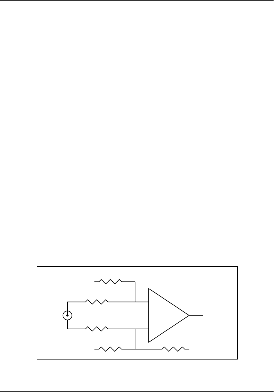
Hardware Installation
RVP8 User’s Manual
May 2003
2–32
2.5 RVP8 Custom Interfaces
This section describes some additional points of interface to the RVP8. These hookups are less
conventional than the “standard” interfaces described earlier in this chapter, but they sometimes
can supply exactly what is needed in exactly the right place. For the most part, these custom
interfaces are merely taps into existing internal signals that would not normally be seen by the
user.
2.5.1 Using the IFD Coax Uplink
The Coax Uplink is the IFD’s single line of communication from the RVP8/Rx processor board.
All of the information that is needed by the IFD arrives through this uplink; and as such, this
signal might contain information that is also useful for other parts of the radar system. In
particular, it is a convenient source of digital AFC, along with reset and other status bits, plus
limited trigger timing information.
The uplink is a single digital transmission line that carries a hybrid serial protocol. The two
logic states, “zero” and “one” are represented by 0-Volt and +15-Volt (open circuit) electrical
levels. The output impedance of the uplink driver is approximately 55Ω. When the cable is
terminated in 75Ω by an internal resistor in the IFD, the overall positive voltage swing will be
approximately 8.6-Volts.
The electrical characteristics of the uplink have been optimized for balanced “groundless”
reception, so that external noise and ground loop currents will not be introduced into the IFD.
The recommended eavesdropping circuit is shown in Figure 2–4, and consists of a high speed
comparator (Maxim MAX913, or equivalent) and input conditioning resistors. Both the shield
and the center conductor of the coax uplink feed the comparator through 33KΩ isolation
resistors; no direct ground attachment is made to the shield itself. The 500Ω resistors provide
the local ground reference, and the 47KΩ resistor supplies a bias to shift the unipolar uplink
signal into a bipolar range for the comparator.
Figure 2–4: Recommended Receiving Circuit for the Coax Uplink
Max913
or equiv.
33KW
33KW
500W
500W
47KW
Received
TTL
Signal
+5V
GND
GND
Coax
Uplink
Input

Hardware Installation
RVP8 User’s Manual
May 2003
2–33
The uplink signal, shown in Figure 2–5, is periodic at the radar pulse repetition frequency, and
conveys two distinct types of information to the IFD. The signal is normally low most of the
time (to minimize driver and termination power), but begins a transition sequence at the
beginning of each transmitted pulse.
Figure 2–5: Timing Diagram of the IFD Coax Uplink
12 345678910...
tburst tststststs
The first part of each pulse sequence is a variable length “burst window” which is centered on
the transmitted pulse itself, and which has a duration tburst approximately 800ns greater than the
length of the current FIR matched filter. The burst window defines the interval of time during
which the IFD transmits digitized burst pulse samples, rather than digitized IF samples, on its
fiber downlink. The exact placement and width of the burst window will depend on the trigger
timing and digital filter specifications that the user has chosen, usually via the Pb and Ps plotting
setup commands.
Following the burst window is a fixed-length sequence of 25 serial data bits which convey
information from the RVP8/Rx board. The first four data bits form a characteristic (0,1,1,0)
marker pattern. The first zero in this pattern effectively marks the end of the variable length
burst window, and the other three bits should be checked for added confidence that a valid bit
sequence is being received. Table 2–9 defines the interpretation of the serial data bits.
Table 2–9: Bit Assignments for the IFD Coax Uplink
Bit(s) Meaning
1–4 Marker Sequence (0,1,1,0). This fixed 4-bit sequence identifies the start
of a valid data sequence following the variable-length burst window.
5–20 16-bit multi-purpose data word, MSB is transmitted first (See below)
21 Reset Request. This bit will be set in just one transmitted sequence
whenever an RVP8 reset occurs.
22 If set, then interpret the 16-bit data word as 4-bits of command and
12-bits of data, rather than as a single 16-bit quantity (See below)
23–24 Diagnostic select bits. These are used by the RVP8 power-up diagnostic
routines; they will both be zero during normal operation.
25 Green LED Request; 0=Off, 1=On. The state of this bit normally
follows the “Fiber Detect” LED on the RVP8/Rx board.

Hardware Installation
RVP8 User’s Manual
May 2003
2–34
The period ts of the serial data is (64ńfaq), where faq is the acquisition clock frequency given
in the Mc section of the RVP8 setup menu. For the default clock frequency of 35.975MHz, the
period of the serial data will be 1.779µsec. The logic that is receiving the serial data should first
locate the center of the first data bit at (0.5 ts) past the falling edge at the end of the burst
window. Subsequent data bits are then sampled at uniform ts intervals.
The actual data sampling rate can be in error by as much as one part in 75 while still maintaining
accurate reception. This is because the data sequence is only 25-bits long, and hence, the last
data bit would still be sampled within 1/3 bit time of its center. Having this flexibility makes
it easier to design the receiving logic. For example, if a 5MHz or 10MHz clock were available,
then sampling at 1.8µsec intervals (1:85 error) would be fine. Likewise, one could sample at
1.75µsec based on a 4MHz or 8MHz clock (1:61 error), but only if the first sample were moved
slightly ahead of center so that the sampling errors were equalized over the 25-bit span.
Interpreting the Serial 16-bit Data Word
The serial 16-bit data word has several different interpretations according to how the RVP8 has
been configured, and whether Bit #22 of the uplink stream is set or clear. The evolution of these
different formats has been in response to new features being added to the IFD (Section 2.2), and
the production of the DAFC Digital AFC Module (Section 2.4).
The original use of the uplink data word was simply to convey a 16-bit AFC level, generally for
use with a magnetron system. Bit #22 is clear in this case, and the word is interpreted as a linear
signed binary value. The use of this format is discouraged for new hardware designs, but it will
always remain available to guarantee compatibility with older equipment.
15 14 13 12 11 10 9 8 7 6 5 4 3 2 1 0
| | | | | | | | | | | | | | | | |
| 16–Bit AFC Level | AFC–16
|_______________________________________________________________|
Level 0111111111111111 (most positive AFC voltage)
0000000000000000 (center AFC voltage)
1000000000000000 (most negative AFC voltage)
When the IFD is jumpered for phase locking to an external reference clock, then Bit #22 will be
clear and the data word conveys the PLL clock ratio, and the Positive/Negative deviation sign of
the Voltage Controlled Crystal Oscillator (VCXO). This format is commonly used with klystron
systems, especially when the RVP8 is locking to an external trigger.
15 14 13 12 11 10 9 8 7 6 5 4 3 2 1 0
| | | | | | | | | | | | | | | | |
| |Pos| Numerator – 1 | Denominator – 1 | PLL–16
|___|___|___________________________|___________________________|
Note that the AFC-16 and PLL-16 formats can never be interleaved for use at the same time,
since there would be no way to distinguish them at the receiving end.
Finally, an expanded format has been defined to handle all future requirements of the serial
uplink. Bit #22 is set in this case, and the data word is interpreted as a 4-bit command and 12-bit
data value. A total of 16x12=192 auxiliary data bits thus become available via sequential
transmission of one or more of these words. The CMD/DATA words can also be used along
with one of the AFC-16 or PLL-16 formats, since Bit #22 marks them differently.

Hardware Installation
RVP8 User’s Manual
May 2003
2–35
15 14 13 12 11 10 9 8 7 6 5 4 3 2 1 0
| | | | | | | | | | | | | | | | |
| Command | Data | CMD/DATA
|_______________|_______________________________________________|
Commands #1, #2, and #3 control the 25 output pin levels of the DAFC board. These
transmissions may be interspersed with the PLL-16 format in systems that require both clock
locking and AFC, e.g., a dual-receiver magnetron system using a digitally synthesized COHO.
Note that the entire 25-bits of pin information are transferred synchronously to the output pins
only when CMD=3 is received. This assures that momentary invalid patterns will not be
produced upon arrival of CMD=1 or CMD=2 when the output bits are changing.
CMD=1 Data<0> DAFC output pin 25
Data<6> Fault Input is active high
Data<11:7> Which pin to use for Fault Input (0:None)
CMD=2 Data<11:0> DAFC output pins 24 through 13
CMD=3 Data<11:0> DAFC output pins 12 through 1
These three digital AFC pinmap commands are recommended as a replacement for the original
AFC-16 format in all new hardware designs. If you only need 12-bits of linear AFC, then map
the AFC range into the –2048 to +2047 numeric span, and select binary coding format (See
Section 3.3.6); the 12-bit data with CMD=3 will then hold the required values. To get a full
16-bit value, use a –32768 to +32767 span and extract the full word from both CMD=2 and
CMD=3. Of course, other combinations of bit formats and number of bits (up to 25) are also
possible.
Command #4 is used to control some of the internal features of the IFD. Bits <4:0> configure
the on-board noise generator so that it adds a selectable amount of dither power to the A/D
converters. This noise is bandlimited using a 10-pole lowpass filter so that most of the energy is
within the 150KHz to 900KHz band, with negligible residual power above 1.4MHz. Each of the
five bits switch in additional noise power when they are set, with the upper bits making
successively greater contributions. Bits <6:5> permit the IF-Input and Burst-Input signals to be
reassigned on the fiber downlink.
CMD=4 Data<4:0> Built-in noise generator level
Data<6:5> IF-Input and Burst-Input selection
00 : Normal 01 : Swap IF/Burst
10 : Burst Always 11 : IF Always
2.5.2 Using the (I,Q) Digital Data Stream (Alan)
The (I,Q) data stream that is computed by the FIR filter chips is communicated in real time to
the central CPU. The “IBD<17:0>” data bus and “IBDCLK” clock signals are sourced on the P3
96-pin DIN connector of the RVP8. These TTL signals are normally kept internal to the RVP8,
but some users may have a need to tap into them directly, e.g., to feed a separate data processor
with the demodulated “I” and “Q”.
Making the electrical connections to the (I,Q) data stream is especially easy with the RxNet7
packaging of the RVP8, since the complete set of signals are driven onto a dedicated 68-pin
connector on its backpanel. Moreover, special PECL drivers on that connector make it possible

Hardware Installation
RVP8 User’s Manual
May 2003
2–36
to run the cable over distances as great as ten meters. Please see the RxNet7 User’s Manual for
full details, as this is the recommended approach for driving the (I,Q) data out to an external
device.
If the RVP8’s internal TTL signals are to be used directly, the physical connections must be
made in such a way that no more than 12cm of additional wire length is added at the backplane.
One way to do this would be to plug a custom driver board into an unused RVP8/AUX slot, from
which the IBDxxx signals could be accessed. Another approach would be to mount the RVP8
board(s) in a completely custom backplane enclosure which also includes the user’s equipment
that receives the (I,Q) data stream.
The timing of the clock and data lines is shown in Figure 2–6 for the interval of time after the
start of each transmitted pulse. The 18-bit data bus conveys two special code words at the
beginning of each pulse, followed by (I,Q) for the Burst/COHO sample, followed by (I,Q) from
the receiver. The receiver data continue to flow until the next transmitted pulse restarts the
sequence anew, after a brief (approximately one range bin) clearing period. The data bus can be
sampled on either the falling or rising edge of the clock, as there is an enforced 28ns data hold
time after each rising clock edge. Using the rising clock edge will give the greatest data setup
time, and this is usually preferred.
Figure 2–6: Timing diagram of the (I,Q) Data Stream
New Pulse Code Burst “I” Burst “Q” Bin #1 “I” Bin #1 “Q”
Trigger Code
IBDCLK Data Clock
IBD<17:0> Data Bus
Range Bin Spacing
28ns
Clearing Period
(after last pulse)
82ns
The “New Pulse” code is a unique 18-bit value that signifies the start of each new pulse of data.
This is the only code or data word in which the MSB is zero.
17 16 15 14 13 12 11 10 9 8 7 6 5 4 3 2 1 0
| | | | | | | | | | | | | | | | | | |
| 0 0 0 0 0 0 0 0 0 0 0 0 0 0 0 0 0 0 |
|_______________________________________________________________________|
The “Trigger Code” follows immediately after the “New Pulse” code. It has a “1” in its MSB,
and three different bit fields encoded into its low byte. These fields give information about the
pulse itself. Codes that are not listed below are reserved, and will never appear on the data bus.
17 16 15 14 13 12 11 10 9 8 7 6 5 4 3 2 1 0
| | | | | | | | | | | | | | | | | | |
| 1 0 0 0 0 0 0 0 0 0 | Flags | Bank | Waveform |
|_______________________________________|_______|___________|___________|
The 2-bit “Flags” field tells how this pulse will be used internally by the RVP8. This
information is probably irrelevant to the external data processor, if all that it is doing is
eavesdropping on the received data.

Hardware Installation
RVP8 User’s Manual
May 2003
2–37
01 This is the final pulse of a collection of pulses that will contribute to the next pro-
cessed ray.
The 3-bit “Bank” field tells the major classification of the pulse.
000 Normal pulse
001 Low PRF pulse during Dual-PRF mode
010 Blanked transmitter version of a normal pulse
111 Pulse used for receiver noise measurement (SNOISE Command)
The 3-bit “Waveform” field indicates the minor classification of the pulse.
000 Normal pulse, or first pulse in a multi-part pulse sequence.
001 Indicates that this is an “alternate” pulse. This is the “V” channel for a single-
channel polarization radar in which the receive or transmit polarization alternates
pulse to pulse from “H” to “V”. This is also the longer PRT pulse whenever
DPRT (Dual-PRT) mode is running.
000-111 These incrementing codes will be output for the first eight pulses of any custom
trigger pattern that the user has defined (See Section 6.14). If the custom pattern
is more than eight pulses long, the “111” code will be held until the end of the se-
quence.
The (I,Q) data for the Burst/COHO sample, as well as for the receiver samples, all have the same
floating point format consisting of a 2-bit unsigned exponent (Exp) and 15-bit signed mantissa
(Man).
17 16 15 14 13 12 11 10 9 8 7 6 5 4 3 2 1 0
| | | | | | | | | | | | | | | | | | |
| 1 | Exp | Floating Point Mantissa (Signed) |
|___|_______|___________________________________________________________|
This format does not rely on a “hidden bit” in the mantissa. Rather, the mantissa is simply a
15-bit (generally unnormalized) value between –16384 and +16383, and the encoded floating
point value is:
Value +Man 16Exp
Note that the exponent shifts the value not in increments of one bit, but rather, by four bits (by
factors of 16). The mantissa will always be the largest integer (i.e., greatest relative precision)
that will fit into the fifteen available bits.
The overall dynamic range is 90dB while maintaining at least 66dB SNR within each sample.
However, the format also gracefully underflows by allowing the mantissa to become small when
Exp=0. This greatly extends the dynamic range into weak signals for which high relative
precision is not required on each sample. The usable dynamic range of values over the entire
receiver span is therefore approximately 125dB.