Codan Radio Communications VT-3A130-S-FSH Transmitter User Manual Enhanced AM FM Synthesizer Instruction Manual
Codan Radio Communications Transmitter Enhanced AM FM Synthesizer Instruction Manual
Contents
Enhanced AM FM Synthesizer Instruction Manual

DANIELS
ELECTRONICS LTD.
TM
MT-3 RADIO SYSTEMS
ENHANCED AM/FM
SYNTHESIZER
INSTRUCTION MANUAL
OS(R/T)-3(A/H) 29 - 470 MHz
Covers models:
OST-3H035, OST-3H045, OSR-3H061
OST-3A128, OSR-3A149
OST-3H141, OST-3H162, OSR-3H141, OSR-3H162
OST-3H440, OSR-3H440
Copyright © 2000 Daniels Electronics Ltd. All rights reserved. No part of this publication may be
reproduced, stored in a retrieval system or transmitted in any form or by any means, electronic,
mechanical, photocopying, recording or otherwise, without the prior written consent of Daniels
Electronics Ltd.
DE™ is a registered trademark of Daniels Electronics Ltd. registered in the United States Patent and
Trademark Office.
Issue: 3 Previous Issue: 2
Issue Date: March 2000 Previous Issue Date: March 1998 Daniels Electronics Ltd.
Printing Date: March 2000 Victoria, BC.
Part No.: IM10-OS3AH PRINTED IN CANADA

DE DANIELS
ELECTRONICS
ii Enhanced AM/FM Synthesizer Instruction Manual OS(R/T)-3(A/H) 29 - 470 MHz
Reviewed By:
Quality Assurance:
Claudia
Boorman
_________________
Name Signature Date
NOTE:
The user's authority to operate this equipment could be revoked through any
changes or modifications not expressly approved by Daniels Electronics Ltd.
The design of this equipment is subject to change due to continuous development.
This equipment may incorporate minor changes in detail from the information
contained in this manual.

DEDANIELS
ELECTRONICS
Enhanced AM/FM Synthesizer Instruction Manual OS(R/T)-3(A/H) 29 - 470 MHz iii
TABLE OF CONTENTS Page
1 GENERAL..........................................................................................1-1
1.1 Introduction...................................................................................1-1
1.2 OS(R/T)-3(A/H) Enhanced Synthesizer Family Models ................................1-1
1.3 Performance Specifications .................................................................1-3
1.4 Printed Circuit Board Numbering Convention ...........................................1-4
2 THEORY OF OPERATION......................................................................2-1
2.1 Internal Power and Control (Digital Board)...............................................2-1
2.2 Synthesizer Analog Circuitry (Analog Board)............................................2-1
2.2.1 Common Analog Board Circuitry.......................................................2-1
2.2.2 29 - 71.4 MHz Analog Board Circuitry ................................................2-3
2.2.3 118 - 159.4 MHz Multichannel AM Analog Board Circuitry........................2-3
2.2.4 128 - 174 MHz Analog Board Circuitry................................................2-4
2.2.5 406 - 470 MHz Analog Board Circuitry................................................2-5
2.3 Synthesizer Digital Circuitry (Digital Board) .............................................2-6
2.4 Frequency Control ...........................................................................2-6
2.4.1 BCD Switch Frequency Control ........................................................2-6
2.4.2 Frequency Select Handle Frequency Control..........................................2-7
2.5 Synthesizer Base and Frequency Increment Table .......................................2-7
2.6 5.0/6.25 kHz Channelization. ..............................................................2-8
2.7 8.333 kHz Channelization. .................................................................2-8
2.8 12.5 kHz Channelization....................................................................2-9
3 SYNTHESIZER ALIGNMENT .................................................................3-1
3.1 General ........................................................................................3-1
3.2 Repair Note ...................................................................................3-1
3.3 Recommended Test Equipment.............................................................3-1
3.4 OS(R/T)-3(A/H) Synthesizer Factory Configuration ....................................3-1
3.5 OS(R/T)-3(A/H) Synthesizer Alignment ..................................................3-2
3.5.1 General .....................................................................................3-2
3.5.2 Synthesizer Test Points...................................................................3-2
3.5.3 Synthesizer Removal and Installation...................................................3-3
3.5.4 Circuit Board Removal ...................................................................3-3
3.5.5 Frequency Adjustment and Channel Selection.........................................3-3
3.5.5.1 VHF OS(R/T)-3H 29 - 71.4 MHz VCO Alignment ...............................3-4
3.5.5.2 VHF OS(R/T)-3A 118 - 159.4 MHz Alignment ...................................3-5
3.5.5.3 VHF OS(R/T)-3H 128 - 174 MHz VCO Alignment...............................3-5
3.5.5.4 UHF OS(R/T)-3H 406 - 470 MHz VCO Alignment...............................3-6
3.5.5.5 Reference Frequency Alignment .....................................................3-6
3.5.6 Jumper Configuration ....................................................................3-6

DE DANIELS
ELECTRONICS
iv Enhanced AM/FM Synthesizer Instruction Manual OS(R/T)-3(A/H) 29 - 470 MHz
4 ILLUSTRATIONS AND SCHEMATIC DIAGRAMS....................................... 4-1
4.1 OS(R/T)-3H 29 - 71.4 MHz Analog Board Diagrams .................................. 4-1
4.1.1 OS(R/T)-3H 29 - 71.4 MHz Analog Board Component Layout (Bottom) ........ 4-1
4.1.2 OS(R/T)-3H 29 - 71.4 MHz Analog Board Component Layout (Top) ............ 4-2
4.1.3 OS(R/T)-3H 29 - 71.4 MHz Analog Board Schematic Diagram.................... 4-3
4.2 OS(R/T)-3A 118 – 159.4 MHz Analog Board Diagrams............................... 4-5
4.2.1 OS(R/T)-3A 118 – 159.4 MHz Analog Board Component Layout (Bottom)..... 4-5
4.2.2 OS(R/T)-3A 118 – 159.4 MHz Analog Board Component Layout (Top)......... 4-6
4.2.3 OS(R/T)-3A 118 – 159.4 MHz Analog Board Schematic Diagram ................ 4-7
4.3 OS(R/T)-3H 128 - 174 MHz Analog Board Diagrams.................................. 4-9
4.3.1 OS(R/T)-3H 128 - 174 MHz Analog Board Component Layout (Bottom)........ 4-9
4.3.2 OS(R/T)-3H 128 - 174 MHz Analog Board Component Layout (Top)...........4-10
4.3.3 OS(R/T)-3H 128 - 174 MHz Analog Board Schematic Diagram ..................4-11
4.4 OS(R/T)-3H 406 - 470 MHz Analog Board Diagrams.................................4-13
4.4.1 OS(R/T)-3H 406 - 470 MHz Analog Board Component Layout (Bottom).......4-13
4.4.2 OS(R/T)-3H 406 - 470 MHz Analog Board Component Layout (Top)...........4-14
4.4.3 OS(R/T)-3H 406 - 470 MHz Analog Board Schematic Diagram ..................4-15
4.5 OS(R/T)-3(A/H) Digital Board Diagrams................................................4-17
4.5.1 OS(R/T)-3(A/H) Digital Board Component Layout (Bottom)......................4-17
4.5.2 OS(R/T)-3(A/H) Digital Board Component Layout (Top)..........................4-18
4.5.3 OS(R/T)-3(A/H) Digital Board Schematic Diagram .................................4-19
5 PARTS LISTS..................................................................................... 5-1
5.1 OS(R/T)-3H 29 - 71.4 MHz Analog Board Electrical Parts List....................... 5-1
5.2 OS(R/T)-3(A/H) 118 – 159.4 MHz Analog Board Electrical Parts List .............. 5-5
5.3 OS(R/T)-3H 128 - 174 MHz Analog Board Electrical Parts List ...................... 5-8
5.4 OS(R/T)-3H 406 - 470 MHz Analog Board Electrical Parts List .....................5-11
5.5 OS(R/T)-3(A/H) Digital Board Electrical Parts List ....................................5-14
5.6 OS(R/T)-3(A/H) Synthesizer Mechanical Parts List....................................5-15
6 REVISION HISTORY............................................................................ 6-1

DEDANIELS
ELECTRONICS
Enhanced AM/FM Synthesizer Instruction Manual OS(R/T)-3(A/H) 29 - 470 MHz 1-1
1 GENERAL
1.1 Introduction
The OS-3A/H Synthesizer Module produces a low distortion, high stability, FM modulated (FM
transmitter) or unmodulated (receiver LO, AM transmitter) RF signal covering the frequency bands
of 29 - 50 MHz, 118 - 159.4 MHz, 118 - 174 MHz and 406 - 470 MHz. It achieves ±1 ppm
frequency stability from -40°C to +60°C with its own internal reference, or it can be slaved to an
external 10/9.6 MHz reference signal of desired stability. The OS-3H Synthesizer Module is
provided in eleven models covering three primary frequency bands (see section 1.2). A synthesizer
module can be easily removed for programming, calibration, or repair. Each synthesizer module
contains two circuit boards providing digital and analog functionality. The analog RF circuitry is
fully isolated in a shielded compartment. Three inter-board filtered wire connections provide signal
and power interface. Digital signal and power control is provided through five photo-logic optical
transceivers, further enhancing electrical noise isolation.
1.2 OS(R/T)-3(A/H) Enhanced Synthesizer Family Models
The OS-3A/H Synthesizer module family forms an integral component of the MT-3 receiver and
transmitter product line. In transmitters, the OS-3A/H synthesizer provides a modulated low level
RF signal to the Power Amplifier module. In receivers, the OS-3A/H synthesizer provides a low
noise local oscillator signal that either directly drives the mixer circuitry or drives a buffer amplifier
in order to achieve higher LO mixer drive required for enhanced intermodulation capability. There
are eleven distinct models in the OS-3H Enhanced Synthesizer Family. Note that this manual
provides service and operating information for
all eleven synthesizer family members. It is
important to establish the correct synthesizer model number of interest in order to direct attention to
specific documented information. The specific model number is printed on the synthesizer module
top cover.
The eleven models are described as follows:
Frequency Band: 29 - 50 MHz,
Common
OS-3H0xx
Analog
Board
• OST-3H035 - synthesized, installed in transmitter, 29 - 38 MHz RF output.
• OST-3H045 - synthesized, installed in transmitter, 38 - 50 MHz RF output.
• OSR-3H061 - synthesized, installed in receiver, 50.4 - 71.4 MHz RF output.

DE DANIELS
ELECTRONICS
1-2 Enhanced AM/FM Synthesizer Instruction Manual OS(R/T)-3(A/H) 29 - 470 MHz
Frequency Band: 118 - 159.4 MHz,
AM Multichannel
OS-3H1xx Analog
Board
• OST-3A128 - synthesized, installed in AM transmitter, 118 - 138 MHz RF output.
• OSR-3A149 - synthesized, installed in AM receiver, 139.4 - 159.4 MHz RF output.
Frequency Band: 118 - 174 MHz,
Common
OS-3H1xx Analog
Board
• OST-3H141 - synthesized, installed in FM transmitter, 128 – 152.6 MHz RF output.
• OST-3H162 - synthesized, installed in FM transmitter, 150 - 174 MHz RF output.
• OSR-3H141 - synthesized, installed in FM receiver, 128 – 152.6 MHz RF output.
• OSR-3H162 - synthesized, installed in FM receiver, 150 - 174 MHz RF output.
Frequency Band: 406 - 470 MHz,
Common
OS-3H4xx Analog
Board
• OST-3H440 - synthesized, installed in FM transmitter, 406 - 470 MHz RF output.
• OSR-3H440 - synthesized, installed in FM receiver, 427.4 - 451.4 MHz RF output.
The OS-3A/H Enhanced Synthesizer models are very similar; all models use the same digital board
and mechanical construction. The significant differences between the models relate to the analog
board. There are four different analog boards covering the four frequency bands of 29 - 50 MHz,
118 - 159.4 MHz, 128 - 174 MHz and 406 - 470 MHz respectively. Each model’s specific sub
band of operation in a given frequency band is determined by select components on the
corresponding analog board.

DEDANIELS
ELECTRONICS
Enhanced AM/FM Synthesizer Instruction Manual OS(R/T)-3(A/H) 29 - 470 MHz 1-3
1.3 Performance Specifications
Type: NBFM Single loop synthesizer module. Utilizing low noise
VCO and PLL technology. Compatible with Daniels MT-3
series transmitter and receiver modules.
Frequency Range: 29 MHz - 38 MHz [± 0.5 MHz] (OST-3H035)
Tuning range with no adjustment 38 MHz - 50 MHz [± 1.0 MHz] (OST-3H045)
shown in [ ] brackets. 50.4 MHz - 71.4 MHz [± 1.0 MHz] (OSR-3H061)
118 MHz -138 MHz [Full band] (OST-3A128)
128 MHz – 152.6 MHz [± 2.0 MHz] (OST-3H141, OSR-3H141)
139.4 MHz - 159.4 MHz [Full band] (OSR-3A149)
150 MHz - 174 MHz [± 2.0 MHz] (OST-3H162, OSR-3H162)
406 MHz - 470 MHz [Full band] (OST-3H440)
427.4 MHz - 451.4 MHz [Full band] (OSR-3H440)
Output Power: +5 dBm ±2 dBm into 50Ω
Harmonics: <-30 dBc
Spurious: <-90 dBc
<-70 dBc above 400 MHz
Attack Time: <50 ms (Power down mode)
Hum and Noise: -55 dB
Modulation Sensitivity: 3.0 kHz peak deviation / 400 mVrms input
External Reference Input: External reference input signal via SMB connector J1
Input level 0 dBm ± 3 dB.
Input impedance 50Ω
Input frequency 10.0 MHz or 9.6 MHz selected through
digital board jumper JU1.
Power Requirements: +9.5 Vdc @ 160 mA for FM and 65 mA for AM
Standby mode, TCXO enabled:
+9.5 Vdc @ 14 mA for FM and 4 mA for AM

DE DANIELS
ELECTRONICS
1-4 Enhanced AM/FM Synthesizer Instruction Manual OS(R/T)-3(A/H) 29 - 470 MHz
1.4 Printed Circuit Board Numbering Convention
To ease troubleshooting and maintenance procedures, Daniels Electronics Limited has adopted a
printed circuit board (PCB) numbering convention in which the last two digits of the circuit board
number represent the circuit board version. For example:
• PCB number 43-9120
10 indicates circuit board version 1.0;
• PCB number 50002-
02
indicates circuit board version 2.0.
All PCB's manufactured by Daniels Electronics are identified by one of the above conventions.

DEDANIELS
ELECTRONICS
Enhanced AM/FM Synthesizer Instruction Manual OS(R/T)-3(A/H) 29 - 470 MHz 2-1
2 THEORY OF OPERATION
2.1 Internal Power and Control (Digital Board)
Refer to "OS(R/T)-3(A/H) Digital Board Schematic Diagram" in section 4 page 19. The
synthesizer operates from +9.5 Vdc applied to connector pin P1-2. Total current drain is
approximately 160 mA (65 ma for AM). Power Down control (P2-4) controls the +5.0 Vdc
microcontroller regulator U2 through power MOSFET switch U1. For receiver applications, the
synthesizer is always operating with the enable line P2-4 permanently connected to +9.5 Vdc. In
transmitter applications, pin P2-4 is controlled by MT-3 Transmitter Board jumper J18 which
selects the synthesizer's standby mode. In low current standby mode (< 16/4 mA) approximately
50 ms of transmitter turn on delay from PTT activation must be tolerated (lock time of
synthesizer). For transmitter applications requiring less than 10 ms of turn on delay, the
synthesizer can be made to run continuously. This capability comes at the expense of an additional
160 (65 mA for AM) of transmitter standby current.
2.2 Synthesizer Analog Circuitry (Analog Board)
There are four separate analog circuit boards covering the four frequencies bands of 29 - 50 MHz,
118 - 159.4 MHz, 128 - 174 MHz and 406 - 470 MHz respectively. All four analog boards are
similar in operation and circuit topology with the VCO, Loop Filter, and Output Lowpass Filter
sections being band specific. Refer to "OS(R/T)-3(A/H) Analog Board Schematic Diagram” in
section of this manual.
2.2.1 Common Analog Board Circuitry
This section describes the circuitry common to all versions of the FM Synthesizer Analog Board.
The Analog Board utilizes four optical receivers (U1 - U4), and one optical transmitter (U5) to
provide an isolated data interface to the digital board. In normal operating modes, +9.5 Vdc
Regulator IC U8 provides continuous +5.0 Vdc to the internal TCXO and power control optical
receiver U1. This results in a standby current level of ≈ 10 mA for FM and 4 mA for AM. Primary
power is controlled through activation of optical receiver U1 under control of the digital board
micro controller U4. Regulator U6 provides switched +8.0 Vdc with regulator U7 providing
switched +5.0 Vdc to all analog supply points. Power MOSFET IC U9 works as a clamping
circuit to quickly discharge VCO filter capacitors C32 and C33 when powered down, resulting in
immediate suppression of RF output from the VCO.
The OS-3H enhanced synthesizer is formed around a low power, single chip MC145190
(MC145191) synthesizer IC U10. A 9.6 MHz reference signal is provided from either the internal
TCXO (JU1-B Analog Board), or an external source via SMB connector J1 with jumper JU1-A

DE DANIELS
ELECTRONICS
2-2 Enhanced AM/FM Synthesizer Instruction Manual OS(R/T)-3(A/H) 29 - 470 MHz
(Analog Board) and jumper JU2 (AM Analog Board only) installed. The external reference source
may be 9.6 MHz or 10.0 MHz through selection of jumper JU2 (Digital Board); install jumper
JU2 (Digital Board) for 10.0 MHz reference selection. If an external signal is used for the
reference source, it must be of low phase noise, high stability, with a level of 0 dBm ± 3 dB. A
sinusoidal signal shape is required for an external reference source. A poor quality reference
source will degrade receiver/transmitter performance to unacceptable levels. Transistor Q2 forms a
buffer amplifier having 50Ω input impedance at 10.0 MHz. The internal 9.6 MHz TCXO provides
better than 1 ppm frequency stability from -30°C to +60°C. Fine frequency adjustment is made
through frequency control potentiometer RV1, which is accessible through the synthesizer top
cover.
The 9.6 MHz reference source is divided down to establish a channel selection step size of
5.0/6.25, 12.5, or 25.0 kHz depending on the particular synthesizer model type. A third order
passive loop filter comprised of C37, C38, C39, C45, C49, R36 and R32, is employed to achieve
the required noise performance, modulation, and worst case switching time of 50 ms. A small
sample of RF energy is coupled from the VCO output buffer U16 on the FM analog board or from
Q6 on the AM analog board to the synthesizer IC U10 prescaler input (pin 11). FM modulation of
the VCO from ≈ 100 Hz to 3 kHz, is provided through the baseband input pin P1-1 on Digital
Board. A 1 kHz sine wave with a level of approximately 400 mVrms at P1-1 provides FM
deviation of 3.0 kHz. SMB connector J2 provides an RF output level of approximately +5 dBm
into a 50Ω load.
An optional modulation input is provided through connection P1-18 (Digital Board) and routed to
the Analog board via connection P3. This connection must be coupled to a low impedance, dc
coupled source and provides a phase modulated bandwidth from 0 (DC) to ≈ 50 Hz (PLL loop
filter bandwidth) allowing for specialized applications such as paging or trunking where a separate
low frequency digital/analog modulation channel is required. Phase modulation input pin P1-18 is
routed to the transmitter audio processor spare pin P4-2 via JA4-2 on the MT-3 transmitter main
board. It should be noted that any application of the direct TCXO modulation port transfers the
control of the synthesizer steady state frequency setting to the external modulating source.
Frequency control potentiometer RV1 is effectively removed from the frequency adjust circuitry.
A lock detect LED (LED1) indicates an unlocked PLL condition. An unlocked PLL condition
normally indicates that the VCO is not tuned within the lock in range of the desired channel
frequency. When used in a transmitter, the loss of lock will prevent PTT from keying the power
amplifier module. This prevents transmission of a spurious, unlocked output signal. Adjustment of
tuning capacitor C24 will normally reestablish frequency lock within the synthesizer design
frequency range. Optical transmitter U5 is additionally activated in unlocked conditions and
enables the micro-controller (digital board) to respond to the unlocked PLL state. Note that the
118 – 159.4 MHz and the 406 - 470 MHz Analog Board does not incorporate a VCO tuning
capacitor; the VCO covers the full frequency range without tuning. An unlocked condition in this
case would indicate an attempt to synthesize an invalid channel frequency outside the installed
VCO frequency range.

DEDANIELS
ELECTRONICS
Enhanced AM/FM Synthesizer Instruction Manual OS(R/T)-3(A/H) 29 - 470 MHz 2-3
2.2.2 29 - 71.4 MHz Analog Board Circuitry
Refer to the "OS(R/T)-3H 29 - 71.4 MHz Analog Board Schematic Diagram" located in section 4
page 3 of this manual.
Field effect transistor Q5 provides a VHF negative resistance amplifier/oscillator that is tuned on
frequency by the combination of resonator L5 and a total capacitive reactance presented across L5
through capacitors C62, C63, C64, C23 (Select), variable capacitor C24, and varactor diodes D1
and D2. Fine frequency adjustment is provided by multi-turn trimmer capacitor C24 in conjunction
with coarse frequency jumper selections JU2, JU3, and JU4. Select capacitor values are chosen to
position the operating frequency in one of three bands; 29 - 38 MHz, 38 - 50 MHz, and 50.4 -
71.4 MHz. Varactor diodes D1 and D2 provide oscillator frequency control. PLL voltage feedback
control from the output of the lowpass loop filter controls the VCO frequency through the reverse
biasing of varactor diodes D1 and D2. The PLL control voltage can range from ≈ +1.0 Vdc to
+7.0 Vdc and is normally set to ≈ +4.5 Vdc for the nominal programmed synthesizer center
frequency. Setting the PLL control voltage set point (TP4) is made by adjusting fine frequency
variable capacitor C24 combined with binary weighted lumped capacitor coarse frequency jumpers
(JU2, JU3, JU4). External baseband frequency modulation is provided through connection P1
and a voltage divider network formed by R21 and R22. A large signal division ratio, established
by the resistive dividers R21 and R22, allows low deviation (less than 5 kHz) direct frequency
modulation of the VCO output signal.
The PLL lowpass filter is formed from select component values C37, C38, C39, C45, R32, and
R36. The loop filter response is optimized for switching time, noise, and modulation requirements
specific to each sub-band within the 29 - 71.4 MHz frequency range. The select component values
(including the loop filter) can be found in tabular format as part of the VHF OS-3H 29 - 71.4 MHz
Analog Board Schematic diagram.
RF output power is taken from the source of Q5 and amplified/buffered by U11. U15 provides
further amplification and isolation while delivering ≈ +10 dBm to a six pole lowpass/notch output
filter formed from C53, C57, C58, C59, L11, and L13. The six pole output filter provides a 50
MHz (OST-3H035, OST-3H045 TX) or 80 MHz (OSR-3H061 RX) cutoff frequency which
reduces harmonic output to acceptable levels. SMB connector J2 provides interconnection to the
companion transmitter or receiver with an output level of ≈ +5 dBm.
2.2.3 118 - 159.4 MHz Multichannel AM Analog Board Circuitry
Refer to the "OS(R/T)-3H 118 - 159.4 MHz Analog Board Schematic Diagram" located in section
4 page 7 of this manual.
Field effect transistor Q5 provides a VHF negative resistance amplifier/oscillator that is tuned on
frequency by the combination of tapped resonator L5 and a total capacitive reactance presented
across L5 through capacitors C40 and/or C23 (Select), varactor diodes D6, D7, and varactor

DE DANIELS
ELECTRONICS
2-4 Enhanced AM/FM Synthesizer Instruction Manual OS(R/T)-3(A/H) 29 - 470 MHz
diodes D1 and D2. Coarse frequency adjustment is provided by varactor diodes D6, D7. Select
capacitor values C40 or C23 are chosen to position the operating frequency in one of two bands;
118 - 138 MHz, and 139.4 - 159.4.MHz. Varactor diodes D1 and D2 provide fine oscillator
frequency control. PLL voltage feedback control from the output of the lowpass loop filter controls
the VCO frequency through the reverse biasing of diodes D1 and D2. The PLL control voltage can
range from ≈ +1.0 Vdc to +4.7 Vdc and is normally set to ≈ +3.3 Vdc for the whole range of
synthesizer frequencies. Setting the PLL control voltage set point (TP4) is made by adjusting the
capacitance of varactor diodes D6, D7, which are controlled by a microcontroller U18 through a
digital to analog converter U17. The microcontroller U18 controls the test point TP4, the output of
the PLL Low Pass Filter, and adjusts the output voltage of D/A converter so that the TP4 voltage is
approximately is 3.3Vdc at any frequencies. The microcontroller than goes sleep in order to keep
the power consumption at the low level.
The PLL lowpass filter is formed from select component values C37, C38, C39, C45, R32, and
R36. The loop filter response is optimized for switching time, noise, and modulation requirements
specific to each sub-band within the 118 - 159.4 MHz frequency range. The select component
values (including the loop filter) can be found in tabular format as part of the VHF OS(R/T)-
3(A/H) 118 - 159.4 MHz Analog Board Schematic diagram.
RF output power is taken from the source of Q5 and amplified/buffered by Q6. U11 provides
further amplification and isolation while delivering ≈ +10 dBm to a five pole lowpass output filter
formed from C53, C58, C59, L11, and L12. The five pole lowpass output filter provides a 190
MHz low pass cutoff frequency which reduces harmonic output to acceptable levels. SMB
connector J2 provides interconnection to the companion transmitter or receiver with an output level
of ≈ +5 dBm.
2.2.4 128 - 174 MHz Analog Board Circuitry
Refer to the "OS(R/T)-3(A/H) 128 - 174 MHz Analog Board Schematic Diagram" located in
section 4 page 11 of this manual.
Field effect transistor Q5 provides a VHF negative resistance amplifier/oscillator that is tuned on
frequency by the combination of tapped resonator L5 and a total capacitive reactance presented
across L5 through capacitors C40 and/or C23 (Select), variable capacitor C24, and varactor diodes
D1 and D2. Fine frequency adjustment is provided by multi-turn trimmer capacitor C24. Select
capacitor values C40 or C23 are chosen to position the operating frequency in one of two bands;
128 – 152.6 MHz and 150 - 174 MHz. Varactor diodes D1 and D2 provide oscillator frequency
control. PLL voltage feedback control from the output of the lowpass loop filter controls the VCO
frequency through the reverse biasing of diodes D1 and D2. The PLL control voltage can range
from ≈ +1.0 Vdc to +7.0 Vdc and is normally set to ≈ +4.5 Vdc for the nominal programmed
synthesizer center frequency. Setting the PLL control voltage set point (TP4) is made by adjusting
fine frequency variable capacitor C24. External baseband frequency modulation is provided
through connection P1 and a voltage divider network formed by R21 and R22. A large signal

DEDANIELS
ELECTRONICS
Enhanced AM/FM Synthesizer Instruction Manual OS(R/T)-3(A/H) 29 - 470 MHz 2-5
division ratio, established by the resistive dividers R21 and R22, allows low deviation (less than 5
kHz) direct frequency modulation of the VCO output signal.
The PLL lowpass filter is formed from select component values C37, C38, C39, C45, R32, and
R36. The loop filter response is optimized for switching time, noise, and modulation requirements
specific to each sub-band within the 128 - 174 MHz frequency range. The select component
values (including the loop filter) can be found in tabular format as part of the VHF OS(R/T)-
3(A/H) 128 - 174 MHz Analog Board Schematic diagram.
RF output power is taken from the source of Q5 and amplified/buffered by U11. U15 provides
further amplification and isolation while delivering ≈ +10 dBm to a five pole lowpass output filter
formed from C53, C58, C59, L11, and L12. The five pole lowpass output filter provides
a 190 MHz low pass cutoff frequency which reduces harmonic output to acceptable levels. SMB
connector J2 provides interconnection to the companion transmitter or receiver with an output level
of ≈ +5 dBm.
2.2.5 406 - 470 MHz Analog Board Circuitry
Refer to the "OS(R/T)-3H 406 - 470 MHz Analog Board Schematic Diagram" located in section 4
page 15 of this manual.
The UHF OS(R/T)-3H 406 - 470 MHz synthesizer employs integrated surface mount VCO
modules (designated U17) for full frequency band coverage. Two VCO modules are used to cover
406 - 470 MHz (TX) and 427.4 - 451.4 MHz (RX) for transmitter and receiver UHF applications
respectively. The receiver VCO module is optimized for low phase noise, while the transmitter
VCO is configured with modulation input capability. PLL voltage feedback control from the output
of the lowpass loop filter controls the VCO frequency through Mod I/P (pin 2). The PLL control
voltage can range from ≈ +1.0 Vdc to +7.0 Vdc depending on the selected operating frequency.
External baseband frequency modulation is provided through connection P1 and VCO Mod input
pin 6.
The PLL lowpass filter is formed from select component values C37, C38, C39, C45, R32, and
R36. The loop filter response is optimized for switching time, noise, and modulation requirements
specific to each sub-band within the 406 - 470 MHz frequency range. The select component values
(including the loop filter and VCO type) can be found in tabular format as part of the UHF
OS(R/T)-3H 406 - 470 MHz Analog Board Schematic diagram.
RF output power is taken from the VCO RF output and amplified/buffered by U11. U15 provides
further amplification and isolation while delivering ≈ +10 dBm to a five pole lowpass output filter
formed from C53, C58, C59, L11, and L12. The five pole lowpass output filter provides
a 530 MHz low pass cutoff frequency which reduces harmonic output to acceptable levels. SMB
connector J2 provides interconnection to the companion transmitter or receiver with an output level
of ≈ +5 dBm.

DE DANIELS
ELECTRONICS
2-6 Enhanced AM/FM Synthesizer Instruction Manual OS(R/T)-3(A/H) 29 - 470 MHz
2.3 Synthesizer Digital Circuitry (Digital Board)
Refer to the "OS(R/T)-3(A/H) Digital Board Schematic Diagram" on page 4-19. Microcontroller
U4 provides control of the synthesizer module. It communicates with synthesizer IC U10,
monitors the synthesizer lock detect, manages PTT input/output, and determines the operating
frequency from either four rotary BCD switches or four externally driven channel select lines. The
rotary BCD channel switches are located on the main MT-3 Transmitter or Receiver circuit board.
The Microcontroller U4 also communicates with an external factory programmer through I/O lines
TX DATA (P1-17), RX DATA (P1-9), and BOOTSTRAP (P2-2). The external programmer
places the operating program in non volatile microprocessor memory. It is also used to program 15
user defined channel selections. An internal "watchdog" timer provides robust software protection
in all operating modes.
Data communication between the digital and analog circuit boards is provided by four optical
transmitters (U5 through U8) and one optical receiver (U9). The optical interface provides a fully
isolated inter-board data link designed to eliminate digital noise from disturbing sensitive PLL
circuitry.
2.4 Frequency Control
2.4.1 BCD Switch Frequency Control
Selection of the desired synthesizer output frequency is straight forward. If all four of the channel
select lines CHAN SEL3 - CHAN SEL0 are pulled low (grounded), the synthesizer will scan four
BCD switches connected to SW1 COM - SW4 COM and PC4 - PC7 to establish the operating
frequency. The BCD switches are located on the receiver and transmitter main circuit boards.
* Note: The four channel select lines, CHAN SEL3 - Chan SEL0, are connected via the MT-3
transmitter or receiver main board module connector to the M3 motherboard subrack. These lines
may be used for external frequency control. They are normally pulled low via jumper sets located
on the M3 motherboard subrack.
If the channel select lines are pulled high to +9.5 Vdc in any combination resulting in a binary code
greater than 0000 (all low), then the frequency is established as the preprogrammed entry in a table
containing 15 separate frequency settings. For example; if all the channel select lines are pulled
high then a binary code of 1111 results which selects the frequency entry from the 15th table
position. CHAN SEL3 is the most significant bit of the binary channel selection code. The channel
table is normally programmed at the factory for those applications requiring specialized remote
control of frequency. These programmed channel assignments are stored in non-volatile
microprocessor EEPROM and are not susceptible to inadvertent erasure.
In transmitters, the synthesizer operating frequency is the transmitter operating frequency;
however, for receivers, an IF Offset correction factor (21.4 MHz typically) must be added to or

DEDANIELS
ELECTRONICS
Enhanced AM/FM Synthesizer Instruction Manual OS(R/T)-3(A/H) 29 - 470 MHz 2-7
subtracted from the synthesizer operating frequency in order to determine the actual receive
frequency. Refer to the channel designation table documentation provided with the transmitter or
receiver modules for simplified channel number and frequency information.
2.4.2 Frequency Select Handle Frequency Control
For operation in this mode the external channel select must be set to channel #16. Channel
selection is achieved by pushing the buttons Frequency Increase Ø and Frequency Decrease Œ on
the Frequency Select Handle. The Frequency Select Handle is located on the Front Panel. The user
interface consists of an 8 digit display and 3 pushbuttons. On power up or key press, the
synthesizer is interrogated for the current channel number and channel frequencies. This
information is used to generate the display, and update the synthesizer itself. The module
communicates with the synthesizer using a standard 2 wire serial interface (9600 Baud, 8 bits, no
parity, 1 stop bit). The command protocols are simple ASCII, both to and from the synthesizer.
The frequency value and the channel are displayed on the Front Panel for several seconds only, in
order to conserve power. Another dedicated line allows the handle to temporarily wake up the
synthesizer if it has been powered down. (This is currently only used on the transmitters)
For the detailed information about changing frequency see the "Frequency Select Handle
Instruction Manual".
2.5 Synthesizer Base and Frequency Increment Table
The OS-3A/H Synthesizer operates in frequency increments of 5.0 / 6.25 kHz, 12.5 kHz, or 25
kHz depending on the particular model and band of operation. The Base Frequency is the lowest
frequency of any given synthesizer model.
Model
Number
Freq.
Range
Base
Frequency
Freq.
Increment
OST-3H035 29 - 38 MHz 29 MHz 5.0/6.25 kHz
OST-3H045 38 - 50 MHz 29 MHz 5.0/6.25 kHz
OSR-3H061 50.4 - 71.4 MHz 50.4 MHz 5.0/6.25 kHz
OST-3A128 118 - 138 MHz 118 MHz 25/8.333 kHz
OST-3H141 128 – 152.6 MHz 128 MHz 5.0/6.25 kHz
OST-3H162 150 - 174 MHz 150 MHz 5.0/6.25 kHz
OSR-3H141 128 - 153 MHz 128 MHz 5.0/6.25 kHz
OSR-3A149 139.4 - 159.4 MHz 139.4 MHz 25/8.333 kHz
OSR-3H162 150 - 174 MHz 150 MHz 5.0/6.25 kHz
OST-3H440 406 - 470 MHz 406 MHz 12.5 kHz
OSR-3H440 427.4 - 451.4 MHz 427.4 MHz 12.5 kHz

DE DANIELS
ELECTRONICS
2-8 Enhanced AM/FM Synthesizer Instruction Manual OS(R/T)-3(A/H) 29 - 470 MHz
2.6 5.0/6.25 kHz Channelization.
The operating frequency is determined as follows for Synthesizers having 5.0/6.25 kHz channel
increment capability;
• for BCD switch settings (in the range of 0000
to
4999 , multiply the switch
setting by 5.0 kHz and add it to the synthesizer base frequency.
Example: An OST-3H141 synthesizer has a base frequency of 128 MHz. The
selected channel number is 0988. The
synthesizer
output frequency is:
((988 x 5 kHz) + 128 MHz) = 132.940 MHz
• for BCD switch settings in the range of
5000
to
9999 , subtract 5000 from the
switch setting, multiplying the result by 6.25 kHz and add it to the synthesizer
base frequency.
Example: An OSR-3H162 synthesizer has a base frequency of 150 MHz. The
selected channel number is 7205. The
synthesizer
output frequency is:
((7205-5000) x 6.25 kHz) + 150 MHz) = 163.78125 MHz
The key point to remember is that 5.0 kHz channel increments are selected with BCD
channel switch settings in the range of #0000 through #4999 and 6.25 kHz channel
increments are selected with BCD switch settings in the range of #5000 through #9999.
2.7 8.333 kHz Channelization.
The operating frequency is determined as follows for Synthesizers having 8.333 kHz channel
increment capability;
• Multiply the BCD switch setting by 8.333 kHz and add it to the synthesizer
base frequency.
Example: An OST-3A128 synthesizer has a base frequency of 118 MHz. The
selected channel number is 0231. The synthesizer output frequency is:
[(1200 x 8.333 kHz) + 118 MHz] = 128.000 MHz

DEDANIELS
ELECTRONICS
Enhanced AM/FM Synthesizer Instruction Manual OS(R/T)-3(A/H) 29 - 470 MHz 2-9
2.8 12.5 kHz Channelization.
The operating frequency is determined as follows for Synthesizers having 12.5 kHz channel
increment capability;
• Multiply the BCD switch setting by 12.5 kHz and add it to the synthesizer base
frequency.
Example: An OST-3H440 synthesizer has a base frequency of 406 MHz. The
selected channel number is 1978. The synthesizer output frequency is:
((1978 x 12.5 kHz) + 406 MHz) = 430.725 MHz

DE DANIELS
ELECTRONICS
2-10 Enhanced AM/FM Synthesizer Instruction Manual OS(R/T)-3(A/H) 29 - 470 MHz
This Page Intentionally Left Blank

DEDANIELS
ELECTRONICS
Enhanced AM/FM Synthesizer Instruction Manual OS(R/T)-3(A/H) 29 - 470 MHz 3-1
3 SYNTHESIZER ALIGNMENT
3.1 General
OS(R/T)-3(A/H) enhanced synthesizer alignment is simplified by using a Type 84 subrack and RF
extender card/cable to provide receiver or transmitter power and signal interconnection.
Alternatively, +9.5 Vdc may be applied directly to a receiver or transmitter module through
positive connection to pins B6 / Z6, and negative connection to pins B30 / Z30 / B32 / Z32.
Receiver balanced audio (600 Ω) is available at pins B26 and Z26.
3.2 Repair Note
The OS(R/T)-3(A/H) synthesizer employs a high percentage of surface mount components which
should not be removed or replaced using an ordinary soldering iron. Removal and replacement of
surface mount components should be performed only with specifically designed surface mount
rework and repair stations complete with Electro Static Dissipative (ESD) protection.
When removing Surface Mount Solder Jumpers, it is recommended to use solder wick braid in
place of vacuum type desoldering tools. This will help prevent damage to the circuit boards.
3.3 Recommended Test Equipment
Alignment of the synthesizer requires the following test equipment or its equivalent.
Power supply - Regulated +9.5 Vdc at 2 A. Phillips PM 2811
Oscilloscope / Multimeter - Fluke 97 Scopemeter
Radio communications test set - Marconi Instruments 2965A
It is recommended that the radio communications test set be frequency locked to an external
reference (WWVH, GPS, Loran C) so that the internal high stability local oscillator may be
accurately set to within its ±1 ppm frequency tolerance.
3.4 OS(R/T)-3(A/H) Synthesizer Factory Configuration
The OS(R/T)-3(A/H) Synthesizer is factory configured as follows:
• Internal 9.6 MHz reference selected.
• VCO modulation by audio processor enabled (OS
T
TX versions only)

DE DANIELS
ELECTRONICS
3-2 Enhanced AM/FM Synthesizer Instruction Manual OS(R/T)-3(A/H) 29 - 470 MHz
The corresponding internal synthesizer jumper settings are:
Digital Board
• Jumper JU2 not installed 9.6/10 MHz reference frequency, 9.6 MHz selected
• Jumper JU1 installed AM Multichannel mode selected
Analog Board
• Jumper JU1: 'B' position Internal/External reference. Internal selected
• Jumper JU2 not installed Internal/External reference. Internal selected
3.5 OS(R/T)-3(A/H) Synthesizer Alignment
3.5.1 General
Under normal circumstances, synthesizer alignment is accomplished without removing the
synthesizer from the MT-3 Receiver IF/Audio Board or the MT-3 Transmitter Main Board.
Alignment simply involves setting the internal TCXO reference frequency (if one is installed and
the internal reference option enabled). This step is described in "Reference Frequency Alignment"
of section 3.5.5.5. A change in synthesizer operating frequency greater than the maximum tuning
range for a particular model (Refer to Specifications section 1.3) from an initial factory setting
requires a slightly more involved alignment procedure as described in sections 3.5.2 to 3.5.5. To
convert a synthesizer with an internal reference source to a synthesizer requiring an external
reference signal or vice-versa is done through the appropriate selection of jumper JU1 A or B, and
JU2 (Refer to section 3.5.6).
3.5.2 Synthesizer Test Points
Analog
Board
Component
Layout
(Top)
Common to all synthesizer family members.
TP1 +8.0 ± 0.3 Vdc. U6 positive regulator output.
TP2 +5.0 ± 0.1 Vdc. U7 positive regulator output.
TP3 +5.0 ± 0.1 Vdc. U8 positive regulator output (always on).
TP4 PLL error voltage. Ranges from +1.0 to +7.0 Vdc depending on frequency.
Nominally adjusted (C24) to +4.5 Vdc for tuned center channel. UHF/VHF
versions employing integrated VCO modules (OSR-3H440, OST-3H440, OSR-
3A149, OST-3A128) require no adjustment.
Digital
Board
Component
Layout
(Bottom)
TP1 +5.0 ± 0.1 Vdc. U2 positive regulator output (controlled via pin P2-4).
TP2 Microcontroller E clock. 2 MHz logic level square wave.

DEDANIELS
ELECTRONICS
Enhanced AM/FM Synthesizer Instruction Manual OS(R/T)-3(A/H) 29 - 470 MHz 3-3
3.5.3 Synthesizer Removal and Installation
The synthesizer module is fastened to the main board (MT-3 Receiver IF/Audio Board or MT-3
Transmitter Main board) with a single counter sunk Phillips machine screw accessible from the top
cover. Remove this screw to remove the synthesizer module. Using a plastic coated lifting tool,
such as a small screwdriver with the tip covered in heat shrink material, gently lift the synthesizer
module from the main circuit board by applying pressure in a rotating fashion about four corners
of the synthesizer module. It is
important
to gently remove the synthesizer module "straight out" in
order to prevent damage to the connector pins. Installation of the synthesizer is performed in a
fashion reverse to the above procedure. It is important to emphasize the importance of connector
pin alignment prior to any application of reinsertion force. Four corner locating pins assist in
connector pin alignment during installation and removal.
Note: Complete synthesizer alignment can be made without removing the synthesizer. The
alignment procedure starting in section 3.5.5 may now be performed.
3.5.4 Circuit Board Removal
Note: Circuit board removal is not required for tuning purposes.
Using a vacuum desoldering station, desolder connections P1, P2, and P3. Remove SMB
connectors J1 and J2 by desoldering the center pins and removing four M2.0 machine screws.
These connection points are shown in the "OS(R/T)-3(A/H) XXX - XXX MHz Analog Board
Component Layout (Top)" diagrams. Remove seven M2.0 machine screws and carefully remove
the analog circuit board. Removal of the analog circuit board will expose three interboard wire
connections. Carefully remove three ferrite beads and six Teflon washers from the inter-board
connection wires. Attempt to maintain the position of the three interboard wires in order to simplify
re-assembly. The digital board may now be extracted by removing four M2.0 machine screws.
Follow a reverse procedure to re-assemble.
3.5.5 Frequency Adjustment and Channel Selection
Connect a radio communications test set through a short section of low loss 50 Ω coaxial cable to
the synthesizer module SMB RF output jack (J2). Select the desired channel number through the
BCD frequency selection switches on the MT-3 Transmitter Main board or the MT-3 Receiver
IF/audio board (or through .the Frequency Programming Module). Turn the power off and on and
wait a few minutes for the oscillator to completely stabilize. It should be noted that the internal
synthesizer TCXO, if installed, operates continuously (regardless of the TX PTT state) when
installed in a transmitter. This continuous operation results in approximately 10 mA of additional
standby current.
The measured RF output signal should be within ± 1.0 ppm of the specified oscillator frequency at
an output level of +5 dBm. Note that unlocked synthesizer operation will be indicated by an

DE DANIELS
ELECTRONICS
3-4 Enhanced AM/FM Synthesizer Instruction Manual OS(R/T)-3(A/H) 29 - 470 MHz
unstable or spurious RF output signal. The "Unlocked" red LED will also be illuminated when the
PLL is unlocked. Check that the requested channel number is within the frequency range of the
particular synthesizer model. An unlocked condition may be rectified by adjusting the VCO tuning
elements as described in the following procedures (no adjustment requires for the multichannel AM
Synthesizers). Note that there are variations in alignment procedures between the three synthesizer
family members as described in the following sections.
3.5.5.1 VHF OS(R/T)-3H 29 - 71.4 MHz VCO Alignment
Refer to the "OS(R/T)-3H 29 - 71.4 MHz Analog Board Component Layout" diagrams and the
"OS(R/T)-3H 29 - 71.4 MHz Analog Board Schematic Diagram" located in section 4 on pages 1, 2
and 3.
Using a high impedance (10 MΩ) DC Voltmeter, measure the PLL control voltage at TP4 located
on the synthesizer module analog board (top). Access to TP4 is available through the synthesizer
top cover. Using a small standard blade screwdriver, carefully adjust the VCO fine frequency
"TUNE" trimmer capacitor C24 until a test point (TP4) voltage of approximately +2.3 Vdc is
obtained. Measured PLL loop control voltages below approximately +0.5 Vdc and above
approximately +4.5 Vdc indicates an "out of lock" synthesizer condition.
If a test point (TP4) voltage of approximately +2.3 Vdc is unattainable through adjustment to C24,
then the coarse frequency jumpers, JU2-JU4 require modification in order to pull the VCO tune
range within the adjustment range of fine tuning capacitor C24. The top synthesizer cover must be
removed in order to gain access to the coarse frequency jumpers. The coarse frequency jumpers
(JU2-JU4) may be considered to be a selectable binary weighted capacitor element with JU2 being
the most significant "bit" and JU4 being the least significant "bit". The tuning resolution size is
≈12 pF (JU4). If the tuning voltage remains higher than +2.3 Vdc, decrease the tuning jumper
setting by 1 "bit" position and re-adjust C24 in an attempt to achieve +2.3 Vdc at TP4. For
example, if coarse frequency jumpers JU2-JU4 are all installed and represented by 111 then a
decrease by 1 "bit" position (12 pF) is represented by a binary jumper selection of 110; jumper
JU4 is not installed and jumpers JU2, JU3 are installed. Continue to decrease the jumper position
one "bit" at a time until the synthesizer regains lock with TP4 adjusted (C24) for +2.3 Vdc. If the
tuning voltage remains lower than +2.3 Vdc, increase the jumper setting by 1 "bit" position and re-
adjust C24 in an attempt to achieve +2.3 Vdc at TP4. Repeat this procedure until +2.3 Vdc at TP4
is achieved.
It is important to check the loop control voltage at TP4 when multiple synthesizer channels have
been programmed. All channel selections should result in a TP4 voltage within a +1.0 to +4.0 Vdc
range. Adjust the fine tuning capacitor C24 to center multiple channel voltages symmetrically about
+2.3 Vdc. Channel selections beyond the tuning range capability of the synthesizer will result in
unlocked operation. The tuning range capability of all synthesizer models is listed in the
Specifications section (1.3) of this manual.

DEDANIELS
ELECTRONICS
Enhanced AM/FM Synthesizer Instruction Manual OS(R/T)-3(A/H) 29 - 470 MHz 3-5
3.5.5.2 VHF OS(R/T)-3A 118 - 159.4 MHz Alignment
Refer to the "OS(R/T)-3A 118 - 159.4 MHz Analog Board Component Layout" diagrams and the
"OS(R/T)-3A 118 - 159.4 MHz Analog Board Schematic Diagram" located in section 4 on pages
5, 6, and 7.
Using a high impedance (10 MΩ) DC Voltmeter, measure the PLL control voltage at TP4 located
on the synthesizer module analog board (top). Access to TP4 is available through the synthesizer
top cover. The VHF synthesizers operating in the 118 - 159.4 MHz frequency range employ a PIC
microcontroller having no frequency adjustment capability. The OST-3A128 and OSR-3A149
models cover 118-138 MHz, and 139.4 - 159.4 MHz respectively and provide full band coverage
without tuning adjustment.
All channel selections might result in a TP4 voltage within the +3.1 to +3.5 Vdc range. Channel
selections beyond the tuning range capability of the synthesizer will result in unlocked operation
over the temperature range - 40C to + 60C. The tuning range capability of all synthesizer models is
listed in the Specifications section of this manual.
3.5.5.3 VHF OS(R/T)-3H 128 - 174 MHz VCO Alignment
Refer to the "OS(R/T)-3H 128 - 174 MHz Analog Board Component Layout" diagrams and the
"OS(R/T)-3H 128 - 174 MHz Analog Board Schematic Diagram" located in section 4 on pages 9,
10 and 11.
Using a high impedance (10 MΩ) DC Voltmeter, measure the PLL control voltage at TP4 located
on the synthesizer module analog board (top). Access to TP4 is available through the synthesizer
top cover. Using a small standard blade screwdriver, carefully adjust the VCO fine frequency
"TUNE" trimmer capacitor C24 until a test point (TP4) voltage of approximately +2.3 Vdc is
obtained. Measured PLL loop control voltages below approximately +0.5 Vdc and above
approximately +4.5 Vdc indicates an "out of lock" synthesizer condition.
It is important to check the loop control voltage at TP4 when multiple synthesizer channels have
been programmed. All channel selections should result in a TP4 voltage within the +1.0 to +4.0
Vdc range. Adjust the fine tuning capacitor C24 to center multiple channel voltages symmetrically
about +2.3 Vdc. Channel selections beyond the tuning range capability of the synthesizer will
result in unlocked operation. The tuning range capability of all synthesizer models is listed in the
Specifications section of this manual.

DE DANIELS
ELECTRONICS
3-6 Enhanced AM/FM Synthesizer Instruction Manual OS(R/T)-3(A/H) 29 - 470 MHz
3.5.5.4 UHF OS(R/T)-3H 406 - 470 MHz VCO Alignment
Refer to the "OS(R/T)-3H 406 - 470 MHz Analog Board Component Layout" diagrams and the
"OS(R/T)-3H 406 - 470 MHz Analog Board Schematic Diagram" located in section 4 on pages 13,
14 and 15.
Using a high impedance (10 MΩ) DC Voltmeter, measure the PLL control voltage at TP4 located
on the synthesizer module analog board (top). Access to TP4 is available through the synthesizer
top cover. The UHF synthesizers operating in the 406 - 470 MHz frequency range employ
integrated VCO modules having no frequency adjustment capability. The OST-3H440 and OSR-
3H440 models cover 406-470 MHz, and 427.4 - 470 MHz respectively and provide full band
coverage without tuning adjustment. Measured PLL loop control voltages below approximately
+0.5 Vdc and above approximately +7.0 Vdc indicates an "out of lock" synthesizer condition.
It is important to check the loop control voltage at TP4 when multiple synthesizer channels have
been programmed. All channel selections should result in a TP4 voltage within the +1.0 to +7.0
Vdc range. Channel selections beyond the tuning range capability of the synthesizer will result in
unlocked operation. The tuning range capability of all synthesizer models is listed in the
Specifications section of this manual.
3.5.5.5 Reference Frequency Alignment
Adjust the synthesizer TCXO fine frequency potentiometer RV1 until the correct output frequency
is achieved. Access to this potentiometer is made available through an opening in the synthesizer
top cover. An RF power level of approximately +5 dBm should be measured at the synthesizer
module output connector and the frequency should be within ±1 ppm from the desired operating
frequency. Reference frequency adjustments should be made at room temperature (+20°C) after ten
minutes.
3.5.6 Jumper Configuration
Solder jumpers are clearly marked on both the synthesizer digital and analog circuit boards. Refer
the "OS(R/T)-3(A/H) Digital Board Component Layout (Bottom)" diagram in section 4 page 14,
and the applicable "OS(R/T)-3(A/H) Analog Board Component Layout (Top)" diagram for jumper
locations. The following list details the required jumper configuration for the two synthesizer
operating modes:
1)
Internal
reference . Install jumper JU1-B, on Analog Board (Standard). The internal
temperature compensated crystal oscillator (TCXO) provides the reference signal
with a stability less than ±1 ppm from -30°C (Optional -40°C) to + 60°C. (Located
on the Analog Board)

DEDANIELS
ELECTRONICS
Enhanced AM/FM Synthesizer Instruction Manual OS(R/T)-3(A/H) 29 - 470 MHz 3-7
2)
External
reference input
. Install jumper JU1-A, JU2 on Analog Board. This mode
is used in applications requiring better than ±1 ppm frequency stability. An external
9.6/10.0 MHz reference signal must be provided at synthesizer SMB connector J1.
(Located on the Analog Board)
3)
Reference
Frequency
Select
. Install jumper JU2 on Digital Board to select a
10.0 MHz reference frequency. When not installed, the reference frequency
selected is 9.6 MHz. JU2 must not be installed when using the internal 9.6 MHz
TCXO reference. JU2 is used by the microcontroller to establish the correct
reference frequency division ratio. (Located on the Digital Board; The Synthesizer
module must be removed to change jumper JU2)
4)
AM
Multichannel
Synthesizer
Select
. Install jumper JU1 on Digital Board to select
AM Multichannel Synthesizer with Frequency Select Handle. (Located on the Front
Panel)
Remember
: Care must be exercised when installing the reconfigured synthesizer module back into
the transmitter board or the IF/audio board. Pay careful attention to pin alignment before pressing
the synthesizer module into its mating sockets.

DE DANIELS
ELECTRONICS
3-8 Enhanced AM/FM Synthesizer Instruction Manual OS(R/T)-3(A/H) 29 - 470 MHz
This Page Intentionally Left Blank
PCB 50038-02
DATE: FEB 26, 1997
DWG No: OS3H040AT2A
DANIELS
ELECTRONICS VICTORIA, B.C.
TITLE: OS-3H050 ANALOG BOARD THROUGH HOLE BOTTOM LAYOUT
BOARD No.:
DWG REV DATE: JAN 6/99
50038-02
Q5
J211
L4
10µH
L6
10µH
R26
1R2
L9
1.5µH
L8
1.5µH
L10
1.5µH
L3
10µH
L2
10µH
R51
220R
C54
22µF
+C50
22µF
+
C42
22µF
+
R50
180R R40
180R
C45
470nF
L7
4.7µH
C24
1-14pF
C37
1.0µF
C39
1.0µF
L5
SEL
L1
10µH
C38
1.0µF
R36
R32
R33
15K
680R
2K7
LED1
+
TITLE: OS-3H050 ANALOG BOARD THROUGH HOLE BOTTOM DESIGNATION
C48 SEL
C49 22nF
R2
330R
L12
4.7µH
DESIG. TX 29 - 40 MHz
OST - 3H035
C48
TX 39 - 50 MHz
OST - 3H045 RX 50.4 - 71.4 MHz
OSR - 3H061
TRANSMITTER RECEIVER
260 nH
L5
68 nF
197 nH
68 nF
138 nH
Not Installed
DE DANIELS
ELECTRONICS
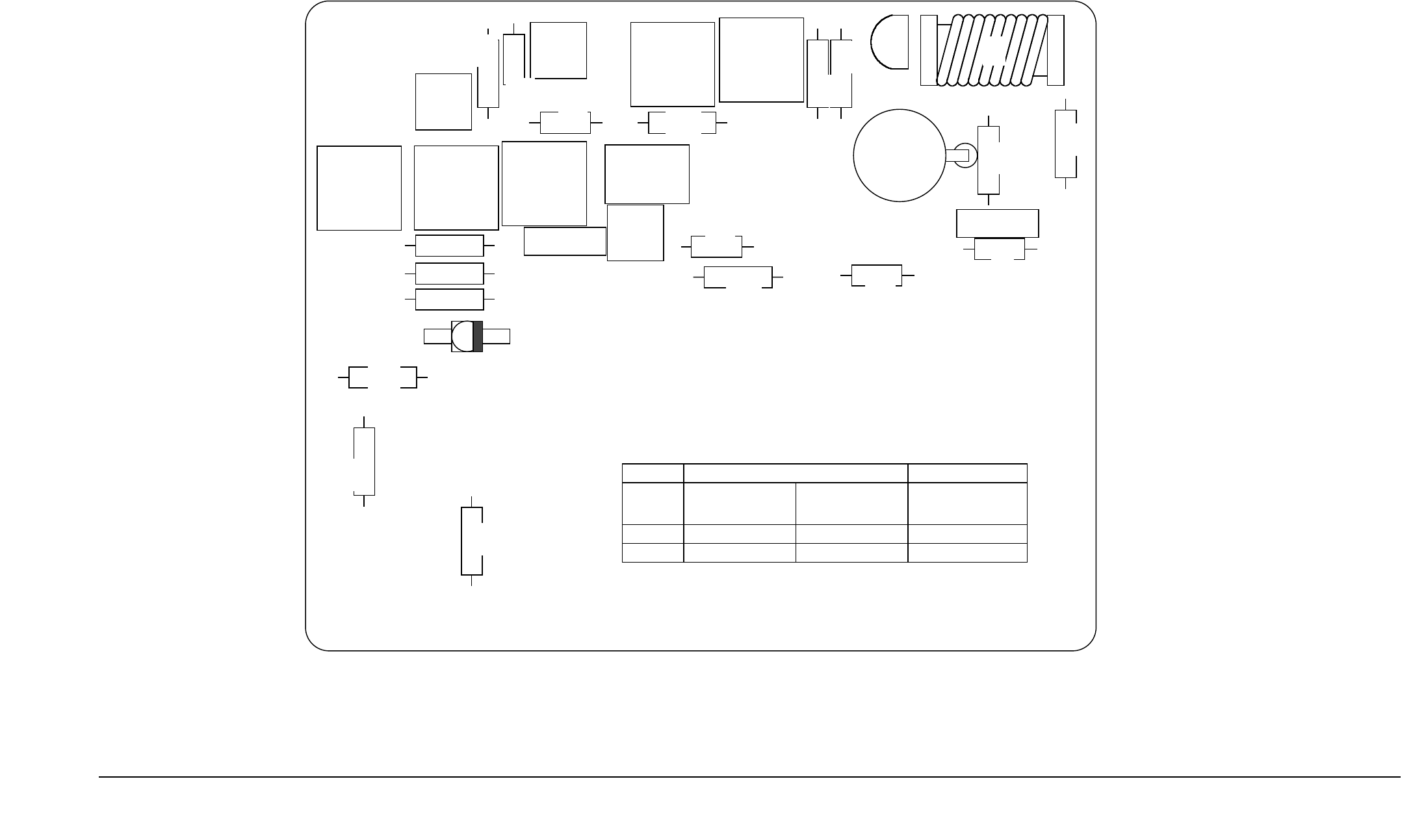
Enhanced AM/FM Synthesizer Instruction Manual OS(R/T)-3(A/H) 29 - 470 MHz 4-1
4 ILLUSTRATIONS AND SCHEMATIC DIAGRAMS
4.1 OS(R/T)-3H 29 - 71.4 MHz Analog Board Diagrams
4.1.1 OS(R/T)-3H 29 - 71.4 MHz Analog Board Component Layout (Bottom)
OS3050M1
PCB 50038-02
DATE: FEB 27, 1997
DWG No:OS3HANA040AS1A
DANIELS
ELECTRONICS VICTORIA, B.C.
TITLE: OS-3H040 ANALOG BOARD SURFACE MOUNT TOP LAYOUT
BOARD No.:
DWG REV DATE: JANUARY 6/1999
50038-02
TITLE: OS-3H040 ANALOG BOARD GENERIC SM TOP DESIGNATIONS
C1
1nF
R14
10k0
R13
11k8
C6
47µF
C2
1nF
C7
10nF
C12
U6
LT1129-IS8
4.7µF
Q1
BC817
R3
10k0
C3
1nF
R4
10k0
R34
10k010k0
R35
10k0
C19
10nF
R23
10R0
U7
LP2951
U8
LP2951
U10
MC145191
C21
10nF
C22
10nF C20
4.7µF
C29
47µF
C30
10nF
R29
18k2
U9
SI9945DY
R15
10R010R0
R24
10R0
4.7µF
C13
4.7µF
C15
4.7µF
C27
4.7µF
R12
10k0
1µF C22
10nF
C26
1nF
R10
10k0
10k0
R18
C11
Q3
BC807
100nF
C5
Q4
BC817
10k0
R11
47µF
C18
100nF
C10
10k0
R19 D5
BAS16
JU1
1nF
C16
5k11
R17
5k11
R16
100nF
C8
100R
R5R5
5k0
RV1
C26
1nF
C31
R9
1k00 R6
1k00
R7
10k0
C14
10nF
Q2
BC817
R8
10k0
10nF
C9
1nF
C25
49R9
R1
20k0
R21
10k0
R53
10R0
R25
10nF
C4
1nF
C17 0R0
R39
D1 D2
MMBV609L
MMBV609L
10R0
R20
15K0
R27
C28
1nF
MMBD701L
SEL
C23
D3
SEL
C34
C35
3.3pF
C36
330pF
R31
49R9
R30
10R0
C44
330pF
C47
330pF
R4118R2
R47
47R5
R48
27R4
R49
33R2
C44
C55
10nF
R52
49R9
C56
330pF R28
N/I
U11
MSA-0611
U16
MSA-0611
MSA-0611
U15 SEL
L13
SEL
L11
C57
SEL
274R
R55
274R
R56
18R2
R54
SEL
C58
SEL
C52
330pF C53
C46
330pF330pF
C51
10nF
27R4
R45
10nF
C43
47R5
R44
47R5
R46
33R2
D4
BYD17J
47pF
C62
JU2 JU3 JU4
22pF
C63 12pF
C64
SEL
C61
33pF
C40
49R9
R38
C41
1nF
SEL
C59
10nF
R22
DESIG. TX 29 - 40 MHz
OST - 3H035
C23 150 pF
15 pF
C53
56 pF
C57
150 pF
C34
C61
TX 39 - 50 MHz
OST - 3H045 RX 50.4 - 71.4 MHz
OSR - 3H061
TRANSMITTER RECEIVER
33 pFC59
33 pFC58
56 pF
100 pF
15 pF
47 pF
100 pF
33 pF
33 pF
56 pF
56 pF
68 pF
33 pF
56 pF
100 pF
68 pF
Not Installed
100 nH
100 nH
L11
L13
100 nH
100nH
120 nH
120 nH
DWG No:OS3HANA040AS2A
475R
TCXO1
TITLE: OS-3H040 ANALOG BOARD TH TOP LAYOUT
U2
OPL550
U3
OPL550 U4
OPL550 U1
OPL550 U5
OP140A
J1
J2
TITLE: OS-3H040 ANALOG BOARD TH TOP DESIGNATION
DE DANIELS
ELECTRONICS
BAR located on
bottom side of TCXO
4-2
4.1.2 OS(R/T)-3H 29 - 71.4 MHz Analog Board Component Layout (Top)
TP2
TP3
TP1
TP4
Enhanced AM/FM Synthesizer Instruction Manual OS(R/T)-3(A/H) 29-470 MHz
OS3050M2B
Desolder three board
interconnect points to
separate analog and
digital boards..
Remove seven M2.0
machine screws to
remove analog board.
AB
JU1 position B selected
for internal 9.6 MHz
P2
P1
P3
LOCK DETECT
LED
DESIGNATION OST-3H035
TX 29 - 40 MHz
C23
TRANSMITTER
OST-3H045
TX 39 - 50 MHz OSR-3H061
TX 50.4 - 71.4 MHz
RECEIVER
L5
C61
C48
C53
C58
C59
L11
C34
C57
L13
150 pF
260 nH *
150 pF
68nF *
56 pF
33 pF
33 pF
56 pF
15pF
56 pF
138 nH *
56 pF
Not Installed
68 pF
100 pF
120 nH
33 pF
120nH
Not Installed
68 pF
100 pF
47 pF
68nF *
56 pF
15pF
33 pF
33 pF
100 pF
100 nH
100 nH
197 nH *
* Thru Hole Component
100 nH
100 nH
VICTORIA B.C.
DE DANIELS
ELECTRONICS
DE DANIELS
ELECTRONICS
DWG REV DATE: 7 MAR 00
TP4 LOOP CONTROL
SET FOR ≈ 2.3 VDC
DWG No: OS3050M3B
BOARD No: 50038-02
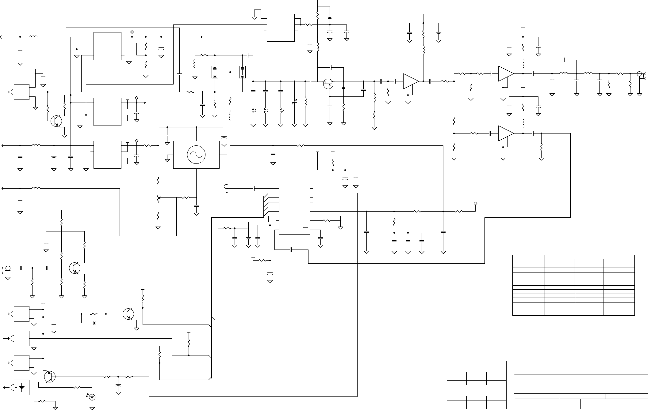
4.1.3 OS(R/T)-3H 29 - 71.4 MHz Analog Board Schematic Diagram
TITLE: OS(R/T)-3H 29 - 71.4 MHz ANALOG BOARD SCHEMATIC DIAGRAM
Enhanced AM/FM Synthesizer Instruction Manual OS(R/T)-3(A/H) 29 - 470 MHz 4-3
-----
-----
U12 - U14
L13
BOARD REV: 1
DATE: 24 FEB 97 DWN BY: COLIN GUNN
LED1
C64
----- -----
R42, R43R37
A
B
U16TCXO1RV1
R56Q5
D5
APRVD:
----- -----
UNUSED REFERENCE DESIGNATORS
HIGHEST REFERENCE DESIGNATORS
RF OUTPUT
3.5 dB Pad
LOCK DETECT
OUTPUT
ACTIVATED WHEN
UNLOCKED
NC
NC
NC
MODULATION INPUT
POWER CNTRL
ID≈10 mA
LOCK DETECT
DATA INPUT
CLK
ENABLE
ACTIVE HIGH
TO ALL +8VA SUPPLY POINTS
EXTERNAL REFERENCE
INPUT (50Ω)
FREQ CONTROL
TCXO MOD INPUT
+9.5 VDC SUPPLY
TO ALL +5VA SUPPLY POINTS
NC
NC
REFOUT
LD
øR
øV
VPD
PDOUT
GND
RX
TEST 1
FIN
REFIN
DIN
CLK
ENB
OUTPUTA
OUTPUTB
VDD
TEST 2
VCC
FIN
1
2
3
4
5
6
7
8
9
1011
12
13
14
15
16
17
18
19
20
U10
MC145191
AGND
AGND
GND
VCNTRL
OUTPUT
VCC
1
4
2
39.6 MHz
TCXO1
AGND
1.0nF
C31
18K2
R29
OUTPUT
SENSE
5VTAP
FB
INPUT
ERROR
SHDN
GND
1
2
6
74
3
5
8
LP2951
U8
AGND
+
4.7uF
C15
AGND
10R0
R15
+
47uF
C18
AGND
5K11
R16
5K11
R17
AGND
5K0
RV1
AGND
1.0nF
C16
+47uF
C6
AGND AGND
10nF
C7
10K0
R19
10nF
C14
AGND
2
1
3
JU1
10nF
C19
+5VA Z2
AGND
10nF
C22
AGND
10nF
C21
10R0
R23
10R0
R24
+
4.7uF
C27
AGND
+
4.7uF
C20
AGND
+5VA
+5VA
49R9
R31
AGND
+
100uF
C32
AGND
10R0
R30
330pF
C36
AGND
IN OUT
GND
13
42
MSA-0611
U11
180R
R40
1.5uH
L8
+22uF
C42
AGND
10nF
C43
AGND
+8VA
330pF
C44 18R2
R41
47R5
R44
47R5
R47
33R2
R46
AGND
330pF
C46
AGND
IN OUT
GND
13
42
MSA-0611
U15
180R
R50
1.5uH
L9
+22uF
C50
AGND
10nF
C51
AGND
+8VA
330pF
C52
27R4
R45
330pF
C47
AGND
IN OUT
GND
13
42
MSA-0611
U16
220R
R51
1.5uH
L10
+
22uF
C54
AGND
10nF
C55
AGND
+8VA
330pF
C56
27R4
R48
33R2
R49
AGND
49R9
R52
AGND
274
R55
AGND
18R2
R54
274
R56
AGND
J2
AGND
2
1
3
MMBV609L
D2
2
1
3
MMBV609L
D1
10uH
L4
10R0
R20
AGND
10R0
R25
10uH
L6
1.0nF
C25
AGND
SEL
C23
10uH
L2
AGND
1.0nF
C2
P2
OUTPUT
SENSE
5VTAP
FB
INPUT
ERROR
SHDN
GND
1
2
6
74
3
5
8
LP2951
U7
AGND
+4.7uF
C13
AGND
10uH
L3
AGND
1.0nF
C3
P3
E
B
C
BC817
Q2
J1
10K0
R7
1K00
R6
1K00
R9
AGNDAGND
10nF
C4 10nF
C9
AGND 49R9
R1
AGND
100R
R5
100nF
C8
AGND
+5VA
VCC
OUT
GND
1
2
3
OPL550
U1
VCC
OUT
GND
1
2
3
OPL550
U2
VCC
OUT
GND
1
2
3
OPL550
U3
VCC
OUT
GND
1
2
3
OPL550
U4
AGND
AGND
AGND
+5VA
100nF
C10
AGND
OUTB
OUTA
ENB
CLK
DIN
AGND
AGND
11K8
R13
10K0
R14
AGND
+4.7uF
C12
AGND
+8VA
AGND
+5VB
100nF
C5
AGND
+5VB
TP1
TP2
TP3
E
B
C
BC817
Q1
AGND
10K0
R4
10K0
R3
OUTPUT
ADJ
GND
NC
VIN
GND
GND
SHDN
8
7
6
54
3
2
1
U6
LT1129-IS8
+
100uF
C33
AGND
BYD17J
D4
1R2
R26
AGND
E
B
C
BC817
Q4
10K0
R11
AGND
10K0
R18
+5VA
ENB
CLK
1
2
U5
OP140A
10K0
R12
AGND
AGND
E
B
CQ3
BC807
10K0
R10
330R
R2
1.0uF
C37
AGND
+8VA
N/I
R28
+
47uF
C29
AGND AGND
10nF
C30
OUTB
L1
10uH
AGND
C1
1.0nF
P1
AGND
475R
R22
AGND
R21
20K0
C26
1.0nF
D1
D1
D2
D2
S1
G1
S2
G2
1
2
3
45
6
7
8
U9
SI9945DY
AGND
R39
0R00
10K0
R8
R34
10K0
R35
10K0
+5VA
+5VA
AGND
+ C11
1.0uF
D5
BAS16
R53
10K0
TP4
1.0uF
C38
AGND AGND
DIN
LTL-93BEK1
LED1
AGND
680R
R33
G
SD
J211
Q5
4.7uH
L7
15K0
R27
MMBD701
D3 33pF
C40
SEL
C34
49R9
R38
1.0nF
C28
+8VA
1.0nF
C41
SEL
L5
1-14pF
C24
JU2
C61
SEL
SEL
C59
SEL
C53
SEL
L11
SEL
C58
AGND AGND
C48
SEL
AGND AGND AGND AGND AGND AGND
AGND
AGND
AGND
JU3 JU4
L13
SEL
C57
SEL
AGND
1nF
C17
47pF
C62 22pF
C63 12pF
C64
15K0
R32
C39
1.0uF
R36
2K7
470nF
C45 22nF
C49
4.7uH
L12
3.3pF
C35
+5VA

D
EDANIELS
ELECTRONICS
4-4 Enhanced AM/FM Synthesizer Instruction Manual OS(R/T)-3(A/H) 29 - 470 MHz
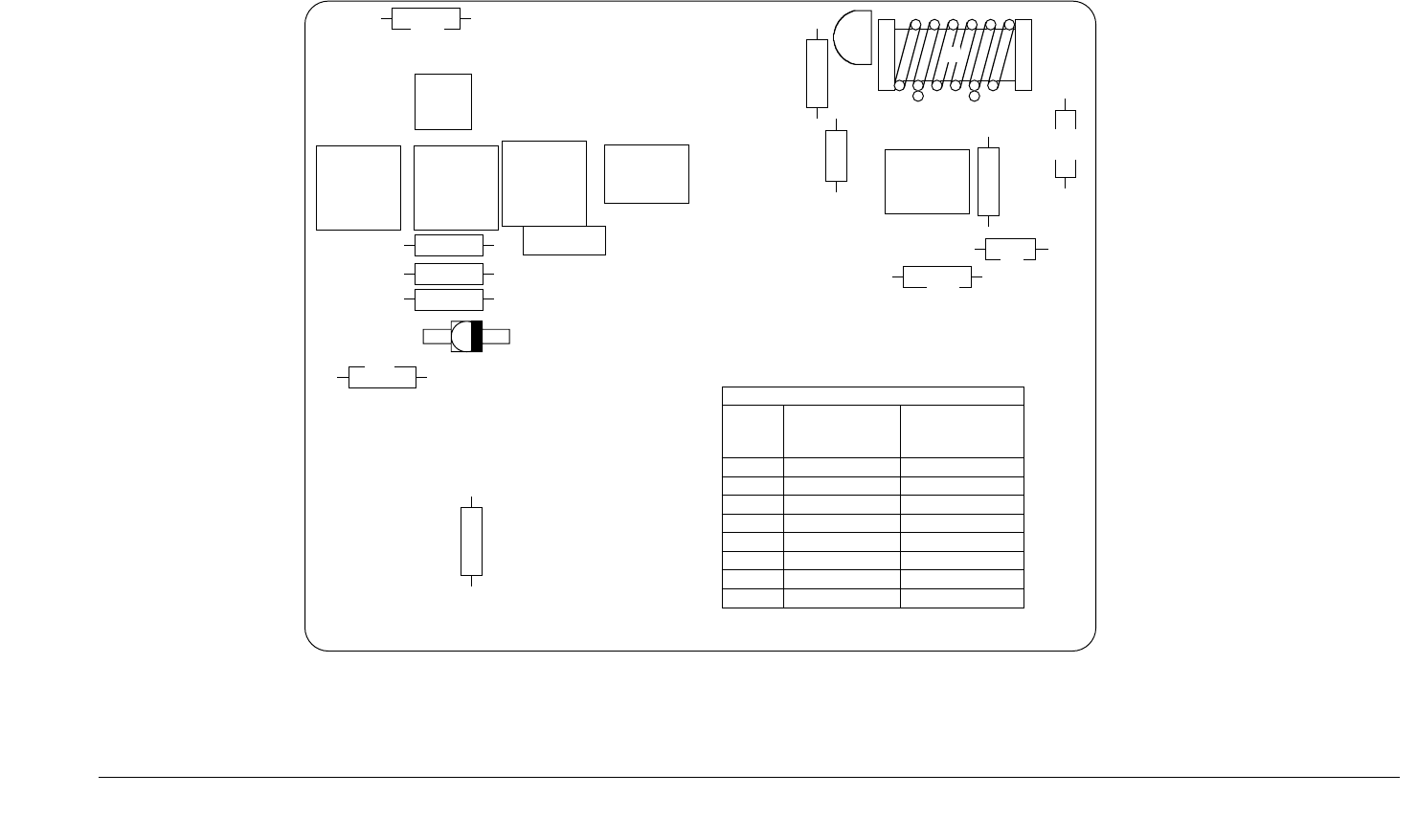
This Page Intentionally Left Blank
DATE: APR 18, 1999
DWG No:TBA
DANIELS
ELECTRONICS VICTORIA, B.C.
TITLE: OS-3A130 ANALOG BOARD OUTLINE
BOARD No.:
DWG REV DATE: 22 DEC 99
50082-05
PCB 50082-05
DWG No:TBA
TITLE: OS-3A130 ANALOG BOARD BOTTOM THROUGH HOLE LAYOUT
L4
1.5µH
L6
1.5uH
R26
1R2
L8
1.5uH
L3
10uH
L2
10uH
C42
22uF
+
C45
SEL
L7
1.5uH
C37
SEL
C39
SEL
L5
R2
330R
C38
SEL
C49 SEL
R36
R32
R33
SEL
680R
SEL
LED1
+
AM TX
118 - 138 MHz
OST - 3A130-10
AM RX
139.4 - 159.4 MHz
OSR - 3A130-10
DESIG.
C39
C45
C49
R32
R36
SELECT COMPONENTS
NOT INSTALLED
22 nF2.2 nF
1.0 µF
330 nF 470 nF
15K68K
1K88K2
C38 100 nF 1.0 µF
C37 470 nF 1.0 µF
Q5
J211
- --
L13
1.5uH
C63
680nF
DWG No:TBA
TITLE: OS-3A130 AM WIDEBAND ANALOG BOARD BOTTOM T.H. DESIGNATIONS
DWG No:OS3A130AT5
Enhanced AM/FM Synthesizer Instruction Manual OS(R/T)-3(A/H) 29 - 470 MHz 4-5
4.2 OS(R/T)-3A 118 - 159.6 MHz Analog Board Diagrams
4.2.1 OS(R/T)-3A 118 - 159.6 MHz Analog Board Component Layout (Bottom)
OS3130M1A
DE DANIELS
ELECTRONICS
DATE: APR 18, 1999
DWG No:OS3AxxxxxS1A
DANIELS
ELECTRONICS VICTORIA, B.C.
TITLE: OS-3A130 ANALOG BOARD OUTLINE
BOARD No.:
DWG REV DATE: FEB 23/2000
50082-05
PCB 50082-05
DWG No:OS3A130S6
TITLE: OS-3A130 ANALOG BOARD SURFACE MOUNT LAYOUT
C51
R14
10k0
R13
11k8
C6
47µF
C2
1nF
C7
10nF
C12
U6
LT1129-IS8
4.7µF
Q1
BC817
R3
10k0
C3
1nF
R4
10k0
R34
10k010k0
R35
10k0
C19
10nF
R23
10R0
U7
LP2951
U8
LP2951
U10
MC145191
C21
10nF
C22
10nF C20
4.7µF
C29
47µF
C30
10nF
R29
18k2
U9
SI9945DY
R15
10R010R0
R24
10R0
4.7µF
C13
4.7µF
C15
4.7µF
C27
4.7µF
R12
10k0
1µF C22
10nF
C26
1nF
R10
10k0
10k0
R18 C11
Q3
BC807
100nF
C5
Q4
BC817
137k
R53
47µF
C18
137k
R42
10k0
R19
D5
BAS16
JU1
1nF
C16
5k11
R17
5k11
R16
100nF
C8 100R
R5R5
5k0
RV1
C26
1nF
C31
R9
1k00
R6
1k00 R7
10k0
C50
100nF
Q2
BC817
R8
10k0
10nF
C9
N/I
C25
49R9
R1
10R0
R25
10nF
C4
0R0
R39
D1 D2
MMBV609L
MMBV609L
10R0
R20
SEL
C23
11k8
R27
C28
6.8µF
MMBD701L
SEL
C40
D3
C34
10nF
C35
SEL
C36
3.3pF
R31
49R9
R30
10R0
100nF
C47
330pF
R41
20k0
C52
10nF
C41
R28
10R0
MSA-0611
U11
47nH
L12
47nH
L11
27pF
C59
27pF
47pF
C58
27pF
C44
330pF
C53
C46
100nF
18R2
R45
10nF
R44
1k82
R46
475R
D4
BYD17J
D6
SEL
4.7µF
C61
10nF
C62 274K
R57 4k75
R62
C60
2.2µF
U17
LTC1257I
U19
MC33172
U18
PIC12C672
SEL
R60
R58
825K
R59
10K0
R63
10R0
137k
R43
R37
49k9
100µF
C32 100µF
C33
D7
SEL
1nF
C1
1nF
C17
100nF
C48
10nF
C14
U20
74HC14 100nF
C10
137k
R22
10k
R11
100nF
R38
49k9
JU2
20K0
R61
1nF
C24
Q6
MMBR901
C43
Factory Installed Jumpers
DWG No:OS3A130S5
TITLE: OS-3A130 ANALOG BOARD SURFACE MOUNT DESIGNATIONS
DWG No:OS3A130AT1
TITLE: OS-3A130 AM WIDEBAND ANALOG BOARD TOP T. H. LAYOUT
U2
OPL950 U3
OPL950 U4
OPL950 U1
OPL950 U5
OP140A
TCXO1
R40
SEL
DWG No:OS3A130AT2
TITLE: OS-3A130 AM WIDEBAND ANALOG BOARD TOP T. H. DESIGNATIONS
C23
SELECT COMPONENTS
AM TX
118 -138 MHz
OST - 3A128
AM RX
139.4 -159.4 MHz
OSR - 3A149
SMV1211
Not Installed
10pF Not Installed
8.2pF
D6-SMV1212, D7-N/I
68K139K2R60
D6,D7
C40
330R220RR40
C35 3.3pF 5.6pF
DESIG.
DE DANIELS
ELECTRONICS
BAR located on
bottom side of TCXO
4-6
4.2.2 OS(R/T)-3A 118 - 159.6 MHz Analog Board Component Layout (Top)
TP2
TP3
TP1
TP4
Enhanced AM/FM Synthesizer Instruction Manual OS(R/T)-3(A/H) 29 - 470 MHz
OS3130M2A
Desolder three board
interconnect points to
separate analog and
digital boards..
Remove seven M2.0
machine screws to
remove analog board.
Select values
AB
JU1 position B selected
for internal 9.6 MHz
P2
P1
P3
LOCK DETECT
LED
J1
J2
DESIG.
C23 *
C39
R36
R32
C49
C40 *
C37
C38
10 pF
NOT INSTALLED
8K2
68K
2.2 nF
NOT INSTALLED
470 nF
100 nF
NOT INSTALLED
1.0 µF
1K8
15K
22 nF
8.2 pF
1.0 µF
1.0 µF
AM RX 139.4-159.4 MHz
OSR-3A149
* - Surface Mount Components
D6*, D7* SMV1211 D6 - SMV1212, D7 - N/I
R60 * 39K2 68K1
AM TX 118-138 MHz
OST-3A128
C45 330 nF 470 nF
R40 220R 330R
C35 * 3.3pF 5.6pF
VICTORIA B.C.
DE DANIELS
ELECTRONICS
DE DANIELS
ELECTRONICS
4.2.3 OS(R/T)-3A 118 - 159.4 MHz Analog Board Schematic Diagram
BOARD REV: 5.0
TITLE: OS(R/T)-3(A/H) 118 - 159.6 MHz ANALOG BOARD SCHEMATIC DIAGRAM
DWG No: OS3130M3 DWG REV DATE: 22 FEB 2000
BOARD No: 50082-05
TP4 LOOP CONTROL
SET FOR ≈3.3 VDC
DWN BY: STAN POLYAKOV
C63
R54-R56
R21, R47-R52
U12 - U16
L1, L9, L10C54 - C57
U20
R63Q6
L13D7
DATE: 06 JULY 99
C32 AND C33 ARE SURFACE MOUNT
OR THROUGH HOLE PARTS
TO ALL +5VB SUPPLY POINTS
TO ALL +5VA SUPPLY POINTS
Enhanced AM/FM Synthesizer Instruction Manual OS(R/T)-3(A/H) 29 - 470 MHz 4-7
A
B
TCXO1RV1
LED1
APRVD:
----- -----
-----
-----
UNUSED REFERENCE DESIGNATORS
HIGHEST REFERENCE DESIGNATORS
RF OUTPUT
LOCK DETECT
OUTPUT
ACTIVATED WHEN
UNLOCKED
NC
NC
NC
POWER CNTRL
ID≈10 mA
LOCK DETECT
DATA INPUT
CLK
ENABLE
ACTIVE HIGH
TO ALL +8VA SUPPLY POINTS
EXTERNAL REFERENCE
INPUT (50Ω)
FREQ CONTROL
TCXO MOD INPUT
+9.5 VDC SUPPLY
NC
NC
REFOUT
LD
øR
øV
VPD
PDOUT
GND
RX
TEST 1
FIN
REFIN
DIN
CLK
ENB
OUTPUTA
OUTPUTB
VDD
TEST 2
VCC
FIN
1
2
3
4
5
6
7
8
9
1011
12
13
14
15
16
17
18
19
20
MC145191
U10
AGND
AGND
GND
VCNTRL
OUTPUT
VCC
1
4
2
3
TCXO1
9.6 MHz
AGND
C31
1.0nF
OUTPUT
SENSE
5VTAP
FB
INPUT
ERROR
SHDN
GND
1
2
6
74
3
5
8
U8
LP2951
AGND
+C15
4.7uF
AGND
R15
10R0
+C18
47uF
AGND
R16
5K11
R17
5K11
AGND
32
1
RV1
5K0
AGND
C16
1.0nF
+C6
47uF
AGND AGND
C7
10nF
R19
10K0
C14
10nF
AGND
2
1
3
JU1
C19
10nF
+5VA Z2
AGND
C22
10nF
AGND
C21
10nF
R23
10R0
R24
10R0
+C27
4.7uF
AGND
+
C20
4.7uF
AGND
+5VA
+5VA
GS
D
Q5
J211
AGND
C34
10nF
AGND
L7
1.5uH
+
C32
100uF
AGND
R30
10R0
+8VA
AGND
L8
1.5uH
+ C42
22uF
AGND
C43
10nF
AGND
+8VA
C44
330pF
L11
47nH L12
47nH
C53
27pF C58
47pF C59
27pF
AGND AGND AGND
J2
AGND
2
1
3D2
MMBV609L
2
1
3
D1
MMBV609L
L4
1.5uH
R20
10R0
AGND
R25
10R0
C25
SEL
AGND
C23
SEL
L2
10uH
AGND
C2
1.0nF
P2
OUTPUT
SENSE
5VTAP
FB
INPUT
ERROR
SHDN
GND
1
2
6
74
3
5
8
U7
LP2951
AGND
+ C13
4.7uF
AGND
L3
10uH
AGND
C3
1.0nF
P3
E
B
C
Q2
BC817
J1
R7
10K0
R6
1K00
R9
1K00
AGND
AGND
C4
10nF
C9
10nF
AGND
R1
49R9
AGND
R5
100R
C8
100nF
AGND
+5VA
AGND
AGND
AGND
AGND
AGND
R13
11K8
R14
10K0
AGND
+ C12
4.7uF
AGND
Z1
+8VA
AGND
+5VB
AGND
+5VB
TP1
TP2
TP3
E
B
C
Q1
BC817
AGND
R4
10K0 R3
10K0
OUTPUT
ADJ
GND
NC
VIN
GND
GND
SHDN
8
7
6
54
3
2
1
LT1129-IS8
U6
+
C33
100uF
AGND
D4
BYD17J
R26
1R2
E
B
C
Q4
BC817
R11
10K0
AGND
+5VA
1
2
OP140A
U5
R12
10K0
AGND
AGND
E
B
CBC807
Q3
R10
10K0
R2
330R
C45
SEL
R36
SEL
C37
SEL
AGND
R28
10R0
+C29
47uF
AGND AGND
C30
10nF
AGND
1.0nF
C26
D1
D1
D2
D2
S1
G1
S2
G2
1
2
3
45
6
7
8
SI9945DY
U9
AGND
R39
0R0
R8
10K0
10K0
R34
+5VA
+5VA
SEL
C49
AGND
+1.0uF
C11
BAS16
D5
SEL
R32 TP4
C38
SEL C39
SEL
AGND AGND
SEL
C40
DIN
AGND
R33
680R
AGND
C62
10nF
AGND AGND
4
3
2
1
8
U19
MC33172
6
5
7
U19
MC33172
b
R61
20K0
R59
10K0
AGND
C60
2.2uF
R63
10R0
AGND
AGND
VOUT
REF
CLK
DOUT
DIN
LOAD
GND
VCC 1
2
3
4
5
6
7
8
U17
LTC1257I
AGND
R27
11K8
+
C28
6.8uF 1
3
2
MMBD701L
D3
+5VB +5VB
R58
825K0
AGND
AGND
GP5 GP2
GP3
GND
VDD
GP0
GP4
GP1 7
4
8
6
1
3
52
PIC12C672
U18
IN OUT
GND
13
42
U11
MSA-0611
+5VA
49K9
R38
49K9
R37
9.5V
9.5V L6
1.5uH
AGND
1.0nF
C17
1.0nF
C1
AGND
1.0nF
C24
AGND
R60
SEL
A
C
U1
OP950 21 14
7
U20
74HC14
a
AGND
A
C
U2
OP950
A
C
U3
OP950
A
C
U4
OP950
JU2
43
U20
74HC14
b
65
cU20
74HC14
89
dU20
74HC14
AGND
C5
100nF
LED1
C10
100nF
10K0
R35
R18
10K0
1011
74HC14
U20e
1213
74HC14
U20f
AGND
ENB
CLK
DIN
CLK
ENB
330pF
C47
R40
SEL
100nF
C48
AGND
AGND
100nF
C50
100nF
C51
+5VA
E
B
C
MMBR901
Q6
AGND
+8VA
1K82
R44
18R2
R45
AGND
AGND
475R0
R46
3.3pF
C36
SEL
C35
100nF
C41
AGND
10nF
C46
C52
10nF
AGND
R62
4K75
AGND
D6
SEL
D7
SEL
1
4
3
2
L5
AGND
+5VB
+5VB
+5VB
L13
1.5uH
4.7uF
C61
680nF
C63
R22
137K0
R42
137K0
R43
137K0
R53
137K0
20K0
R41
+5VA
R57
274K0
R29
18K2
49R9
R31

D
EDANIELS
ELECTRONICS
4-8 Enhanced AM/FM Synthesizer Instruction Manual OS(R/T)-3(A/H) 29 - 470 MHz
This Page Intentionally Left Blank
PCB 50025-02
DATE: MARCH 22, 1996
DWG No:TBA
DANIELS
ELECTRONICS VICTORIA, B.C.
TITLE: OS-3H ANALOG BOARD THROUGH HOLE BOTTOM LAYOUT
BOARD No.:
DWG REV DATE: 15 MARCH 2000
50025-02
L5
C33
100µF
C32
100µF
L4
1.5µH
L6
1.5µH
R26
1R2
1.5µH
L8
1.5µH
L10
1.5µH
L3
10uH
L2
10µH
R51
220R
C54
22µF
+C50
22µF
+
++
C42
22µF
+
R50
180R
R40
180R
C45
SEL
L7
1.5µH
C24
1-14pF
C37
1.0 µF
C39
SEL
L1
10µH
R2
330R
C38
SEL
C49 SEL
R36
R32
R33
SEL
680R
SEL
LED1
+
TITLE: OS-3H ANALOG BOARD THROUGH HOLE BOTTOM DESIGNATION
L9
VHF LOW BAND
128 - 153 MHz
OSx - 3H141
VHF HIGH BAND
150 - 174 MHz
OSx - 3H162
DESIG.
C39
22 nF
C45
33 nF
NOT INSTALLED
C49
220 nF
15K12KR32
6K22K2R36
SELECT COMPONENTS
C38 1.0 µF 470 nF
1.0 µF
470 nF
Q5
J211 L5
Enhanced AM/FM Synthesizer Instruction Manual OS(R/T)-3(A/H) 29 - 470 MHz 4-9
4.3 OS(R/T)-3H 128 - 174 MHz Analog Board Diagrams
4.3.1 OS(R/T)-3H 128 - 174 MHz Analog Board Component Layout (Bottom)
OS3150M1B
DE DANIELS
ELECTRONICS
PCB 50025-02
DATE: FEB 24, 1996
DWG No:OS3HANA150AS1A
DANIELS
ELECTRONICS VICTORIA, B.C.
TITLE: OS-3H150 ANALOG BOARD ECO #584 CHANGES
BOARD No.:
DWG REV DATE: MARCH 10, 2000
50025-02
Not Inastalled (installed during final assembly)
Factory Installed Jumpers
TITLE: OS-3H150 ANALOG BOARD SURFACE MOUNT TOP DESIGNATIONS
C1
1nF
R14
10k0
R13
11k8
C6
47µF
C2
1nF
C7
10nF
C12
U6
LT1129-IS8
4.7µF
Q1
BC817
R3
10k0
C3
1nF
R4
10k0
R34
10k010k0
R35
10k0
C19
10nF
R23
10R0
U7
LP2951
U8
LP2951
U10
MC145191
C21
10nF
C22
10nF C20
4.7µF
C29
47µF
C30
10nF
R29
18k2
U9
SI9945DY
R15
10R010R0
R24
10R0
4.7µF
C13
4.7µF
C15
4.7µF
C27
4.7µF
R12
10k0
1µF C22
10nF
C26
1nF
R10
10k0
10k0
R18
C11
Q3
BC807
100nF
C5
Q4
BC817
10k0
R11
47µF
C18
100nF
C10
10k0
R19 D5
BAS16
JU1
1nF
C16
5k11
R17
5k11
R16
100nF
C8
100R
R5R5
5k0
RV1
C26
1nF
C31
R9
1k00 R6
1k00
R7
10k0
C14
10nF
Q2
BC817
R8
10k0
10nF
C9
1nF
C25
49R9
R1
20k0
R21
10k0
R53
10R0
R25
10nF
C4
1nF
C17 0R0
R39
100R
R22
D1 D2
MMBV609L
N/I
10R0
R20
SEL
C23 11k8
R27
C28
6.8µF
MMBD701L
SEL
C40
D3
10nF
C34
10nF
C35
SEL
C36
330pF
R31
49R9
R30
10R0
C44
330pF
C47
330pF
R4118R2
R47
47R5
R48
47R5
R49
10R0
C44
C55
10nF
R52
N/I
C56
330pF R28
N/I
U11
MSA-0611
U16
MSA-0611MSA-0611
MSA-0611
U15
47nH
L12
47nH
L11
27pF
C59
27pF
274R
R55
274R
R56
18R2
R54
47pF
C58
27pF
C52
330pF C53
C46
330pF330pF
C51
10nF
27R4
R45
10nF
C43
47R5
R44
47R5
R46
33R2
D4
BYD17J
DWG No:OS3HANA150AS2A
TITLE: OS-3H ANALOG BOARD THROUGH HOLE LAYOUT
DWG No:OS3HANA150AT1
U2
OPL550 U3
OPL550 U4
OPL550 U1
OPL550 U5
OP140A
TITLE: OS-3H ANALOG BOARD THROUGH HOLE DESIGNATION
DWG No:OS3HANA150AT2
C23
C40 12 pF
SELECT COMPONENTS
6.8 pF
6.8 pF
VHF LOW BAND
128 - 153 MHz
OSx - 3H141
12 pF
VHF HIGH BAND
150 - 174 MHz
OSx - 3H162
C35 3.3 pF 8.2 pF
DE DANIELS
ELECTRONICS
C24 Fine Frequency Adjust
BAR located on
bottom side of TCXO
4-10
4.3.2 OS(R/T)-3H 128 - 174 MHz Analog Board Component Layout (Top)
TP2
TP3
TP1
TP4
Enhanced AM/FM Synthesizer Instruction Manual OS(R/T)-3(A/H) 29 - 470 MHz
OS3150M2B
Desolder three board
interconnect points to
separate analog and
digital boards..
Remove seven M2.0
machine screws to
remove analog board.
Select values
AB
JU1 position B Selected
for internal 9.6 MHz
P2
P1
P3
LOCK DETECT
LED
J1
J2
SEL
C35
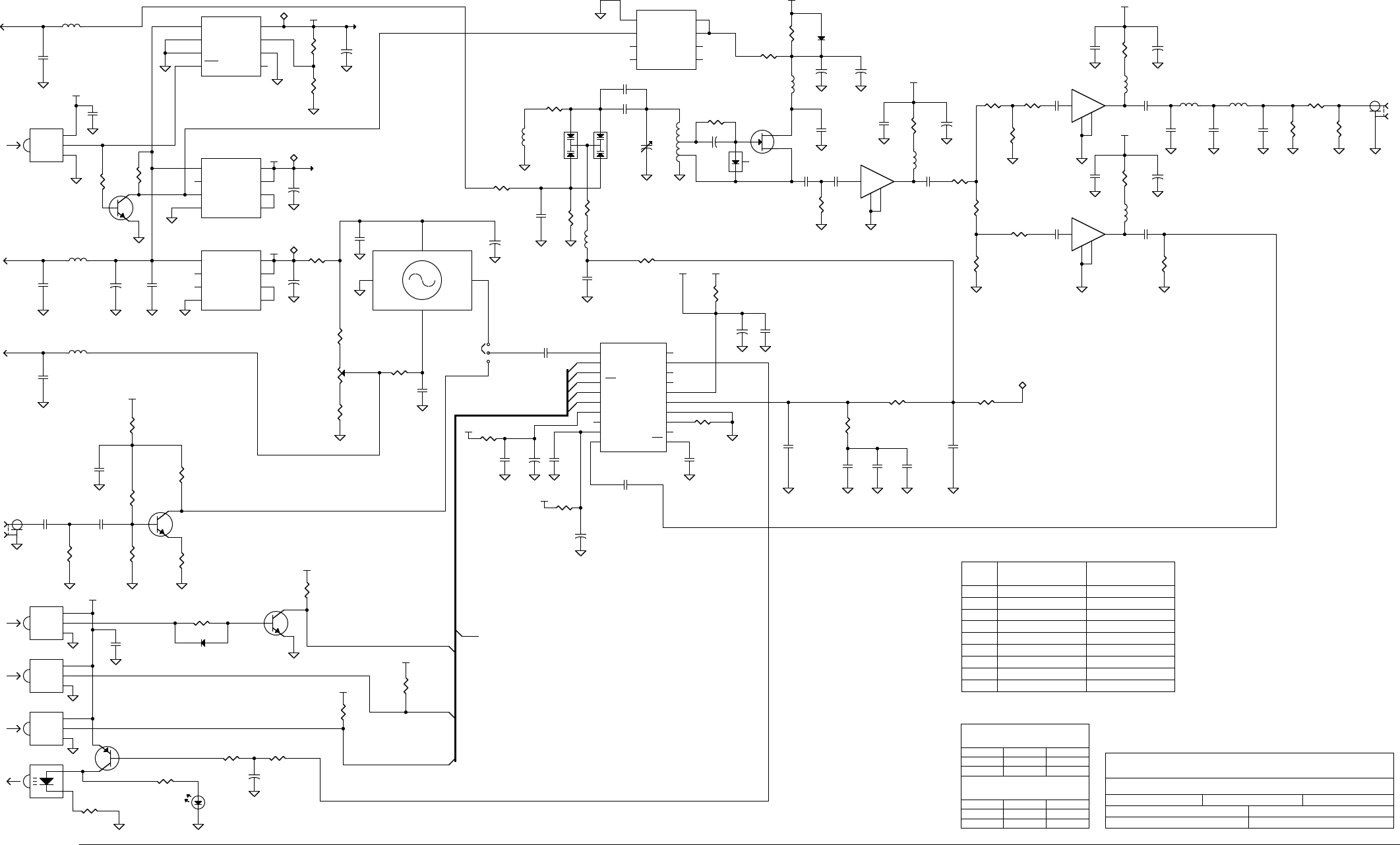
DESIG. LOW BAND 128-153 MHz
OSx-3H141
C23 * 12 pF 6.8 pF
C45 470nF 330 nF
C39 1.0uF 220nF
R36 2K2 3K3
R32 12K 15K
C49 33nF 22nF
C40 * 12 pF 6.8 pF
C38 1.0 µF 1.0 µF
HIGH BAND 150-174 MHz
OSx-3H162
* - Surface Mount Components
C35 * 3.3 pF 8.2 pF
VICTORIA B.C.
DE DANIELS
ELECTRONICS
DE DANIELS
ELECTRONICS
4.3.3 OS(R/T)-3H 128 - 174 MHz Analog Board Schematic Diagram
TITLE: OS(R/T)-3(A/H) 128.6 - 174 MHz ANALOG BOARD SCHEMATIC DIAGRAM
TP4 LOOP CONTROL
SET FOR ≈ 2.3 VDC
DWG REV DATE: 7 MAR 00 DWG No: OS3150M3B
4-11
Enhanced AM/FM Synthesizer Instruction Manual OS(R/T)-3(A/H) 29 - 470 MHz
A
B
U12 - U14R42,R43
R37,R38C57C41,C48
U16TCXO1RV1
R56Q5LED1
L12D5C59
BOARD REV: 2BOARD No: 50025-02
DWN BY: COLIN GUNNDATE: 21 FEB 96 APRVD:
----- -----
-----
-----
UNUSED REFERENCE DESIGNATORS
HIGHEST REFERENCE DESIGNATORS
RF OUTPUT
3.5 dB Pad
LOCK DETECT
OUTPUT
ACTIVATED WHEN
UNLOCKED
NC
NC
NC
MODULATION INPUT
POWER CNTRL
ID≈10 mA
LOCK DETECT
DATA INPUT
CLK
ENABLE
ACTIVE HIGH
TO ALL +8VA SUPPLY POINTS
EXTERNAL REFERENCE
INPUT (50Ω)
FREQ CONTROL
TCXO MOD INPUT
+9.5 VDC SUPPLY
TO ALL +5VA SUPPLY POINTS
NC
NC
REFOUT
LD
øR
øV
VPD
PDOUT
GND
RX
TEST 1
FIN
REFIN
DIN
CLK
ENB
OUTPUTA
OUTPUTB
VDD
TEST 2
VCC
FIN
1
2
3
4
5
6
7
8
9
1011
12
13
14
15
16
17
18
19
20
U10
MC145191
AGND
AGND
GND
VCNTRL
OUTPUT
VCC
1
4
2
39.6 MHz
TCXO1
AGND
1.0nF
C31
18K2
R29
OUTPUT
SENSE
5VTAP
FB
INPUT
ERROR
SHDN
GND
1
2
6
74
3
5
8
LP2951
U8
AGND
+
4.7uF
C15
AGND
10R0
R15
+
47uF
C18
AGND
5K11
R16
5K11
R17
AGND
32
1
5K0
RV1
AGND
1.0nF
C16
+47uF
C6
AGND AGND
10nF
C7
10K0
R19
10nF
C14
AGND
2
1
3
JU1
10nF
C19
+5VA Z2
AGND
10nF
C22
AGND
10nF
C21
10R0
R23
10R0
R24
+
4.7uF
C27
AGND
+
4.7uF
C20
AGND
+5VA
+5VA
GS
D
J211
Q5
SEL
C35
49R9
R31
AGND
11K8
R27
1
4
3
2
L5
AGND
+
6.8uF
C28
10nF
C34
AGND
1
3
2
D3
MMBD701L
1.5uH
L7
+
100uF
C32
AGND
10R0
R30
330pF
C36
C24
1-14pF
AGND
+8VA
AGND
IN OUT
GND
13
42
MSA-0611
U11
180R
R40
1.5uH
L8
+22uF
C42
AGND
10nF
C43
AGND
+8VA
330pF
C44 18R2
R41
47R5
R44
47R5
R47
33R2
R46
AGND
330pF
C46
AGND
IN OUT
GND
13
42
MSA-0611
U15
180R
R50
1.5uH
L9
+22uF
C50
AGND
10nF
C51
AGND
+8VA
330pF
C52
27R4
R45
330pF
C47
AGND
IN OUT
GND
13
42
MSA-0611
U16
220R
R51
1.5uH
L10
+
22uF
C54
AGND
10nF
C55
AGND
+8VA
330pF
C56
47R5
R48
10R0
R49
AGND
N/I
R52
AGND
47nH
L11 47nH
L12
27pF
C53 47pF
C58 27pF
C59
AGND AGND AGND
274
R55
AGND
18R2
R54
274
R56
AGND
J2
AGND
2
1
3
MMBV609L
D2
2
1
3
N/I
D1
1.5uH
L4
10R0
R20
AGND
10R0
R25
1.5uH
L6
1.0nF
C25
AGND
SEL
C23
10uH
L2
AGND
1.0nF
C2
P2
OUTPUT
SENSE
5VTAP
FB
INPUT
ERROR
SHDN
GND
1
2
6
74
3
5
8
LP2951
U7
AGND
+4.7uF
C13
AGND
10uH
L3
AGND
1.0nF
C3
P3
E
B
C
BC817
Q2
J1
10K0
R7
1K00
R6
1K00
R9
AGNDAGND
10nF
C4 10nF
C9
AGND 49R9
R1
AGND
100R
R5
100nF
C8
AGND
+5VA
VCC
OUT
GND
1
2
3
OPL550
U1
VCC
OUT
GND
1
2
3
OPL550
U2
VCC
OUT
GND
1
2
3
OPL550
U3
VCC
OUT
GND
1
2
3
OPL550
U4
AGND
AGND
AGND
+5VA
100nF
C10
AGND
OUTB
OUTA
ENB
CLK
DIN
AGND
AGND
11K8
R13
10K0
R14
AGND
+4.7uF
C12
AGND
Z1
+8VA
AGND
+5VB
100nF
C5
AGND
+5VB
TP1
TP2
TP3
E
B
C
BC817
Q1
AGND
10K0
R4
10K0
R3
OUTPUT
ADJ
GND
NC
VIN
GND
GND
SHDN
8
7
6
54
3
2
1
U6
LT1129-IS8
+
100uF
C33
AGND
BYD17J
D4
1R2
R26
AGND
E
B
C
BC817
Q4
10K0
R11
AGND
10K0
R18
+5VA
ENB
CLK
1
2
U5
OP140A
10K0
R12
AGND
AGND
E
B
CQ3
BC807
10K0
R10
330R
R2
SEL
C45
SEL
R36
1.0uF
C37
AGND
+8VA
R28
N/I
+
47uF
C29
AGND AGND
10nF
C30
OUTB
L1
10uH
AGND
C1
1.0nF
P1
AGND
C17
1nF R22
100R
AGND
R21
20K0
C26
1.0nF
D1
D1
D2
D2
S1
G1
S2
G2
1
2
3
45
6
7
8
U9
SI9945DY
AGND
R39
0R0
10K0
R8
R34
10K0
R35
10K0
+5VA
+5VA
C49
SEL
AGND
+ C11
1.0uF
D5
BAS16
R32
SEL R53
10K0
TP4
SEL
C38 SEL
C39
AGND AGND
C40
SEL
DIN
LED1
AGND
680R
R33
+5VA

D
EDANIELS
ELECTRONICS
4-12 Enhanced AM/FM Synthesizer Instruction Manual OS(R/T)-3(A/H) 29 - 470 MHz
This Page Intentionally Left Blank
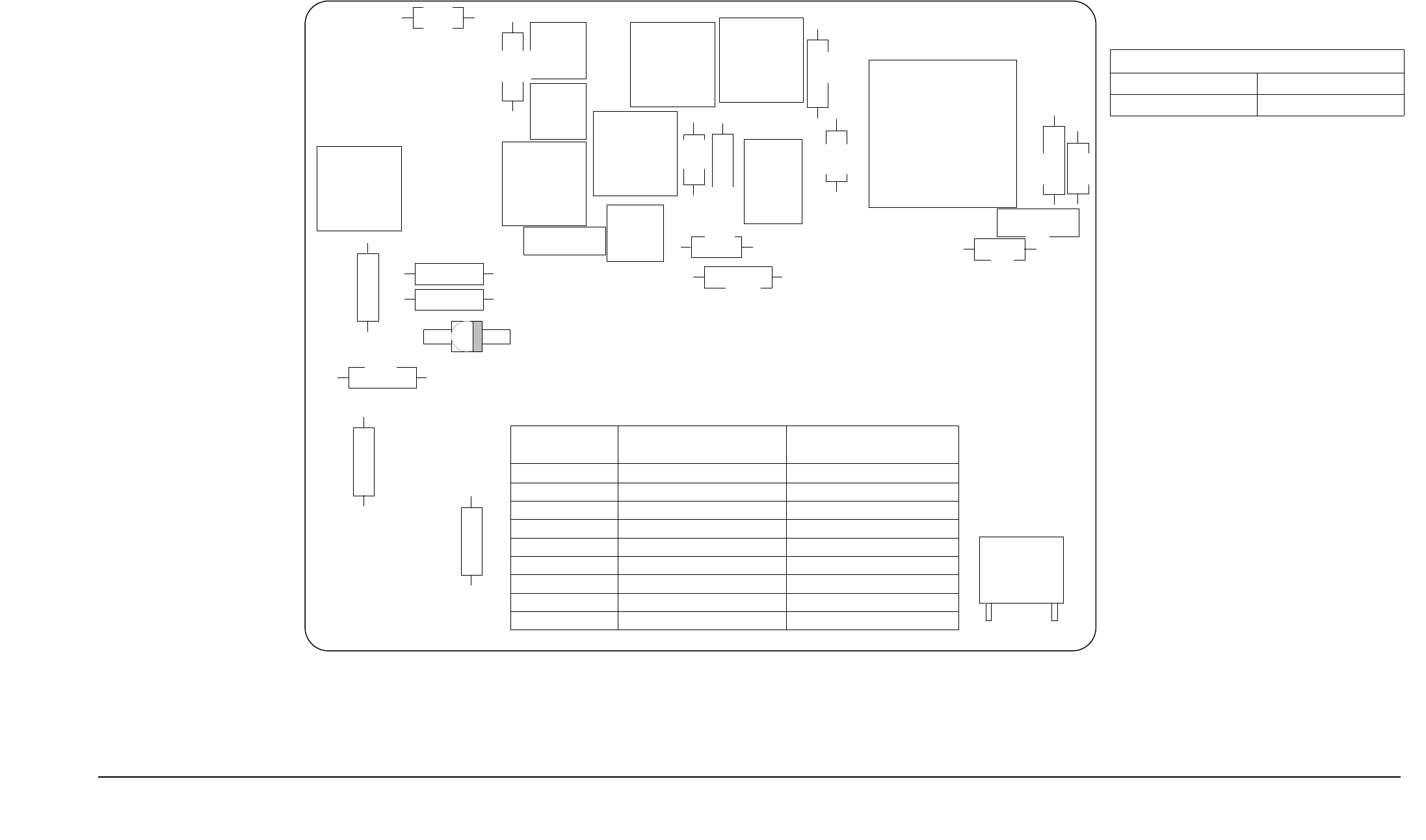
DATE: MARCH 22, 1996
DWG No:TBA
DANIELS
ELECTRONICS VICTORIA, B.C.
TITLE: OS-3H ANALOG BOARD THROUGH HOLE BOTTOM LAYOUT
BOARD No.:
DWG REV DATE: 13 Aug 1997 GM
50028-02
C33
100µF
C32
100µF
L6
1.5µH
R26
1R2
L9
1.5µH
L8
1.5µH
L10
1.5µH
L3
10µH
L2
10µH
R51
220R
C54
22uF
+C50
22µF
+
++
C42
22µF
+
R50
180R
R40
180R C45
SEL
L7
1.5µH
C37
1µF
C39
SEL
L1
10µH
R2
330R
C38
SEL
C49 SEL
R36 R32
R33
SEL
680R
SEL
LED1
+
TITLE: OS-3H ANALOG BOARD THROUGH HOLE BOTTOM DESIGNATION
U17
VCO
1VCO INSTALLED (U17)
LVCO-2309 TEV VCO-190-435 MT
RX 427.4 - 451.4 MHz TX 406 - 470 MHz
R21
SEL
C60
SEL
C16
100nF
DESIGNATION OSR-3H440
RX 427.4 - 451.4 MHz OST-3H440
TX 406 - 470 MHz
C38
C39
C45
C49
C60
R21
R32
R36
1.0 µF
1.0 µF
470 nF
33 nF
Not Installed
Not Installed
4k7
1k5
Not Installed
Not Installed
220 nF
22 nF
100 nF
2k7
5k6
2k2
DE DANIELS
ELECTRONICS
Enhanced AM/FM Synthesizer Instruction Manual OS(R/T)-3(A/H) 29 - 470 MHz 4-13
4.4 OS(R/T)-3H 406 - 470 MHz Analog Board Diagrams
4.4.1 OS(R/T)-3H 406 - 470 MHz Analog Board Component Layout (Bottom)
OS3450M1B
PCB 50028-02
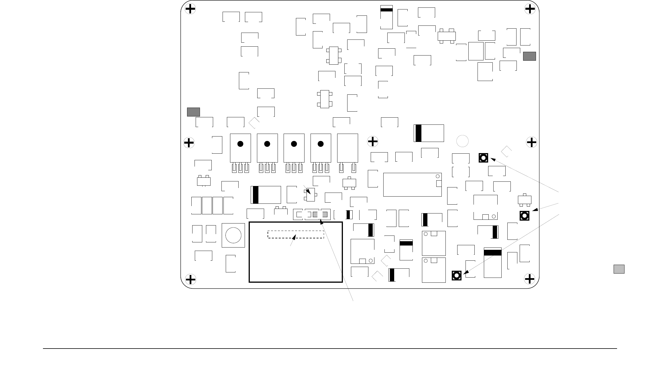
DATE: FEB 24, 1996
DWG No:OS3HANA440AS1
DANIELS
ELECTRONICS VICTORIA, B.C.
TITLE: UHF OS-3H ANALOG BOARD SURFACE MOUNT TOP LAYOUT
BOARD No.:
DWG REV DATE: APR 23, 1997
50028-02
TITLE: OS-3H UHF ANALOG BOARD SURFACE MOUNT TOP DESIGNATIONS
C1
1nF
R14
10k0
R13
11k8
C6
47µF
C2
1nF
C7
10nF
C12
U6
LT1129-IS8
4.7µF
Q1
BC817
R3
10k0
C3
1nF
R4
10k0
R34
10k010k0
R35
10k0
C19
10nF
R23
10R0
U7
LP2951
U8
LP2951
U10
MC145190
C21
10nF
C22
10nF C20
4.7µF
C29
47µF
C30
10nF
R29
36k5
U9
SI9945DY
R15
10R010R0
R24
10R0
4.7µF
C13
4.7µF
C15
4.7µF
C27
4.7µF
R12
10k0
1µF C22
10nF
C26
1nF
R10
10k0
10k0
R18
C11
Q3
BC807
100nF
C5
Q4
BC817
10k0
R11
47µF
C18
100nF
C10
10k0
R19 D5
BAS16
JU1
5k11
R17
5k11
R16
100nF
C8 100R
R5R5
5k0
RV1
C26
1nF
C31
R9
1k00 R6
1k00
R7
10k0
C14
10nF
Q2
BC817
R8
10k0
10nF
C9
1nF
C25
49R9
R1 10k0
R53
10nF
C4
1nF
C17
0R0
R39
10R0
R25
10nF
C34
C35
100pF C36
330pF
R31
274R
R30
10R0
C44
330pF
C47
330pF
R41
18R2
R47
47R5
R48
27R4
R49
33R2
C44
C55
10nF
R52
49R9
C56
330pF R28
10R0
U11
MSA-0611
U16
MSA-0611MSA-0611
U15
18nH
L12
18nH
L11
C59
10pF
274R
R55
274R
R56
18R2
R54
15pF
C58
10pF
C52
330pF
C53
C46
330pF
C51
10nF
27R4
R45
10nF
C43
47R5
R44
47R5
R46
33R2
D4
BYD17J
R57
18R2
R58
274R MSA-0611
Factory Installed Jumpers
DWG No:OS3HANA440AS2
TITLE: UHF OS-3H ANALOG BOARD THOUGH HOLE TOP LAYOUT
U2
OPL550 U3
OPL550 U4
OPL550 U1
OPL550 U5
OP140A
J1
J2
TITLE: UHF OS-3H ANALOG BOARD THOUGH HOLE TOP DESIGNATIONS
TCXO1
DE DANIELS
ELECTRONICS
BAR located on
bottom side of TCXO
4-14
4.4.2 OS(R/T)-3H 406 - 470 MHz Analog Board Component Layout (Top)
Enhanced AM/FM Synthesizer Instruction Manual OS(R/T)-3(A/H) 29 - 470 MHz
OS3450M2
Desolder three board
interconnect points to
separate analog and
digital boards..
JU1 position B selected
for internal 9.6 MHz
P2
P1
P3
TP3
TP1
TP4
AB
LOCK DETECT
LED
TP2
PCB 50028-02
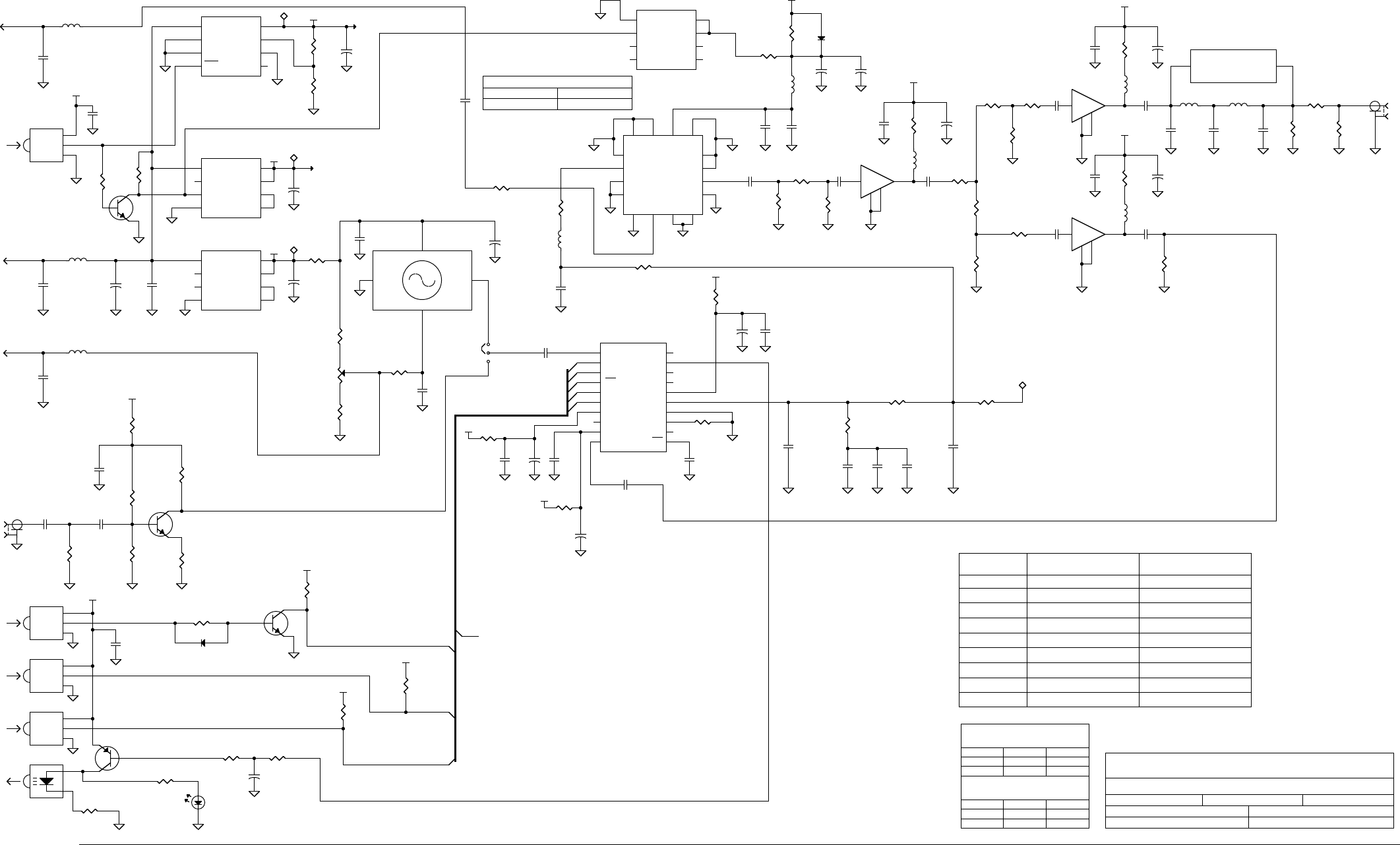
DESIGNATION OSR-3H440
RX 427.4 - 451.4 MHz
OST-3H440
TX 406 - 470 MHz
C38
C39
C45
C49
C60
R32
R36
R21
R32
R36
1.0 µF
1.0 µF
470 nF
33 nF
Not Installed
Not Installed
4k7
1k5
Not Installed
Not Installed
220 nF
22 nF
100 nF
2k7
5k6
2k2
VCO INSTALLED (U17)
LVCO-2309 TEV VCO-190-435 MT
RX 427.4 - 451.4 MHz TX 406 - 470 MHz
VICTORIA B.C.
DE DANIELS
ELECTRONICS
DE DANIELS
ELECTRONICS 4-15
4.4.3 OS(R/T)-3H 406 - 470 MHz Analog Board Schematic Diagram
07 MARCH 00
DWG No: OS3450M3B
BOARD REV: 2.0
A
B
TITLE: OS(R/T)-3H 406 - 470 MHz ANALOG BOARD SCHEMATIC DIAGRAM
Enhanced AM/FM Synthesizer Instruction Manual OS(R/T)-3(A/H) 29 - 470 MHz
C57, R22
C60
L4, L5
J2, JU1
R58, RV1
BOARD No: 50028-02
U17
R38,R42,R43R20,R27,R37
Q4
D1 - D3
C40,C41,C48C23,C24,C28
U12 - U14
DWG REV DATE:
DATE: 23 MAY 96
TCXO1
LED1
L12D5
DWN BY: COLIN GUNN APRVD:
-----
UNUSED REFERENCE DESIGNATORS
HIGHEST REFERENCE DESIGNATORS
TP4 LOOP CONTROL
SET FOR ≈ 4.5 VDC
RF OUTPUT
3.5 dB Pad
LOCK DETECT
OUTPUT
ACTIVATED WHEN
UNLOCKED
NC
NC
NC
MODULATION INPUT
POWER CNTRL
ID≈10 mA
LOCK DETECT
DATA INPUT
CLK
ENABLE
ACTIVE HIGH
TO ALL +8VA SUPPLY POINTS
EXTERNAL REFERENCE
INPUT (50Ω)
FREQ CONTROL
TCXO MOD INPUT
+9.5 VDC SUPPLY
TO ALL +5VA SUPPLY POINTS
NC
NC
REFOUT
LD
øR
øV
VPD
PDOUT
GND
RX
TEST 1
FIN
REFIN
DIN
CLK
ENB
OUTPUTA
OUTPUTB
VDD
TEST 2
VCC
FIN
1
2
3
4
5
6
7
8
9
1011
12
13
14
15
16
17
18
19
20
MC145190
U10
AGND
AGND
GND
VCNTRL
OUTPUT
VCC
1
4
2
3
TCXO1
9.6 MHz
AGND
C31
1.0nF
R29
36K5
OUTPUT
SENSE
5VTAP
FB
INPUT
ERROR
SHDN
GND
1
2
6
74
3
5
8
U8
LP2951
AGND
+C15
4.7uF
AGND
R15
10R0
+C18
47uF
AGND
R16
5K11
R17
5K11
AGND
32
1
RV1
5K0
AGND
C16
100nF
+C6
47uF
AGND AGND
C7
10nF
R19
10K0
C14
10nF
AGND
2
1
3
JU1
C19
10nF
+5VA Z2
AGND
C22
10nF
AGND
C21
10nF
R23
10R0
R24
10R0
+C27
4.7uF
AGND
+
C20
4.7uF
AGND
+5VA
+5VA
C35
100pF
AGNDAGND
C34
10nF
AGND
L7
1.5uH
+C32
100uF
AGND
R30
10R0
C36
330pF
AGND
+8VA
AGND
IN OUT
GND
13
42
U11
MSA-0611
R40
180R
L8
1.5uH
+ C42
22uF
AGND
C43
10nF
AGND
+8VA
C44
330pF
R41
18R2
R44
47R5
R47
47R5
R46
33R2
AGND
C46
330pF
AGND
IN OUT
GND
13
42
U15
MSA-0611
R50
180R
L9
1.5uH
+ C50
22uF
AGND
C51
10nF
AGND
+8VA
C52
330pF
R45
27R4
C47
330pF
AGND
IN OUT
GND
13
42
U16
MSA-0611
R51
220R
L10
1.5uH
+C54
22uF
AGND
C55
10nF
AGND
+8VA
C56
330pF
R48
27R4
R49
33R2
AGND
R52
49R9
AGND
L11
18nH L12
18nH
C53
10pF C58
15pF C59
10pF
AGND AGND AGND
R55
274R
AGND
R54
18R2
R56
274R
AGND
0
1
J2
AGND
AGND
R25
10R0
L6
1.5uH
C25
1.0nF
AGND
L2
10uH
AGND
C2
1.0nF
P2
OUTPUT
SENSE
5VTAP
FB
INPUT
ERROR
SHDN
GND
1
2
6
74
3
5
8
U7
LP2951
AGND
+ C13
4.7uF
AGND
L3
10uH
AGND
C3
1.0nF
P3
E
B
C
Q2
BC817
J1
R7
10K0
R6
1K00
R9
1K00
AGNDAGND
C4
10nF
C9
10nF
AGND R1
49R9
AGND
R5
100R
C8
100nF
AGND
+5VA
VCC
OUT
GND
1
2
3
U1
OPL550
VCC
OUT
GND
1
2
3
U2
OPL550
VCC
OUT
GND
1
2
3
U3
OPL550
VCC
OUT
GND
1
2
3
U4
OPL550
AGND
AGND
AGND
+5VA
C10
100nF
AGND
OUTB
OUTA
ENB
CLK
DIN
AGND
AGND
R13
11K8
R14
10K0
AGND
+ C12
4.7uF
AGND
Z1
+8VA
AGND
+5VB
C5
100nF
AGND
+5VB
TP1
TP2
TP3
E
B
C
Q1
BC817
AGND
R4
10K0 R3
10K0
OUTPUT
ADJ
GND
NC
VIN
GND
GND
SHDN
8
7
6
54
3
2
1
LT1129-IS8
U6
+C33
100uF
AGND
D4
BYD17J
R26
1R2
AGND
E
B
C
Q4
BC817
R11
10K0
AGND
R18
10K0
+5VA
ENB
CLK
1
2
OP140A
U5
R12
10K0
AGND
AGND
E
B
CBC807
Q3
R10
10K0
R2
330R
C45
SEL
R36
SEL
C37
1uF
AGND
+8VA
R28
10R0
+C29
47uF
AGND AGND
C30
10nF
OUTB
10uH
L1
AGND
1.0nF
C1
P1
AGND
1.0nF
C17
SEL
R21
1.0nF
C26
D1
D1
D2
D2
S1
G1
S2
G2
1
2
3
45
6
7
8
SI9945DY
U9
AGND
0R0
R39
R8
10K0
10K0
R34
10K0
R35
+5VA
+5VA
SEL
C49
AGND
+1.0uF
C11
BAS16
D5
SEL
R32 10K0
R53
TP4
C38
SEL C39
SEL
AGND AGND
DIN
LED1
LTL-93BEK1
AGND
R33
680R
AGND
AGND AGND
AGND
Band Pass Filter
(Optional)
12
F1
GND
MOD I/P
GND
GND
GND MOD GND GND
GND
RF OUT
GND
GND
GND VCCGND GND
VCO
1
2
3
4
5678
9
10
11
12
13141516
U17
274R
R58
18R2
R57
274R
R31
C60
SEL

D
EDANIELS
ELECTRONICS
4-16 Enhanced AM/FM Synthesizer Instruction Manual OS(R/T)-3(A/H) 29 - 470 MHz
This Page Intentionally Left Blank
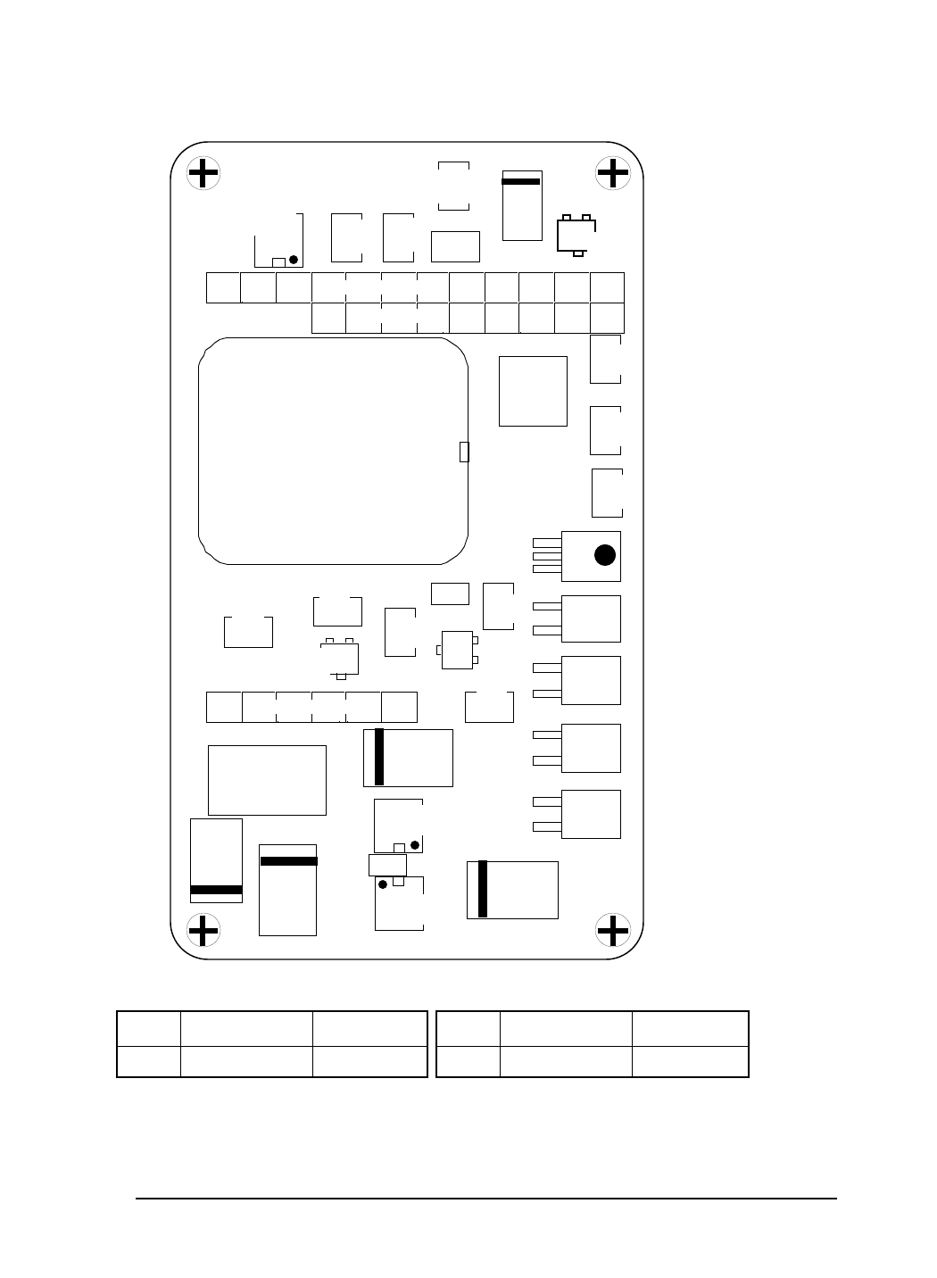
DWG No: OS3HDIGAS3A
TITLE: OS-3H DIGITAL BOARD SOLDER SIDE SM LAYOUT
DATE: 31 MARCH 1997
BOARD No.: 50021-03
REV DATE: 14 SEP 1999
DANIELS
ELECTRONICS VICTORIA, B.C.
C8
4.7uF
U3
MC33064 R8
6k81 R19
27k4
C9
100nF
Q9
BC817
U41
68HC11E2
X1
8.0Mhz
C7
22pF
R11
10M0
C6
22pF
R39
27k4
R4
27k4
R10
27k4 R25
10k0
Q2
BC817
R24
10k0
L1
10uH
C5
47uF
C3
47uF U1
SI9933Y
U2
LP2951
C4
47uF
R6
27k4
D3
BAS16
DWG No: OS3HDIGAS4B
TITLE: OS-3H DIGITAL BOARD SOLDER SIDE SM VALUE / DESIGNATION
JU2
REV DATE: 14 SEPTERMBER 1998
C15
10uF JU1
U9
OPL550
U8
OP140A
U7
OP140A
U6
OP140A
U5
OP140A
P1 1ROW x 12P
1ROW x 9P
P2 1ROW x 6P
4.5 OS(R/T)-3(A/H) Digital Board Diagrams
4.5.1 OS(R/T)-3(A/H) Digital Board Component Layout (Bottom)
DE DANIELS
ELECTRONICS
4-17Enhanced AM/FM Synthesizer Instruction Manual OS(R/T)-3(A/H) 29 - 470 MHz
OS3150M4APCB 50021-03
JU2
9.6 MHz
REFERENCE 10 MHz
REFERENCE
NOT INSTALLED INSTALLED
JU1
OSx-3H
29-470 MHz OSx-3A
118-159.6 MHz
NOT INSTALLED INSTALLED
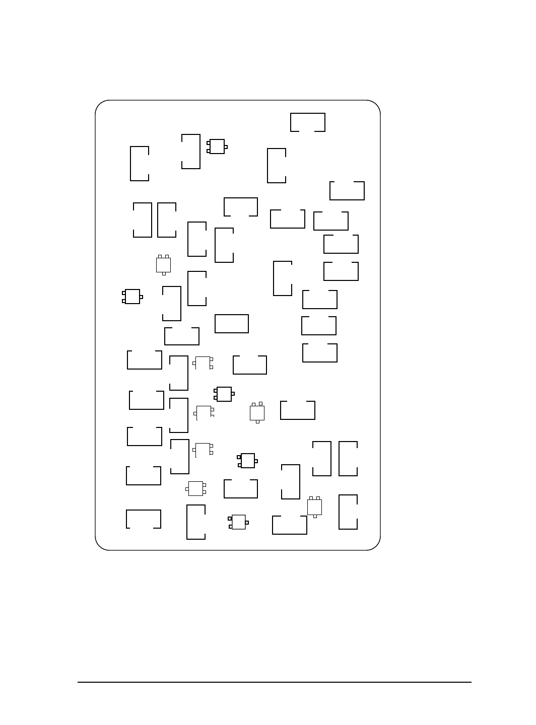
DATE: 25 MARCH 1996
DWG No: OS3HDIGAS
TITLE: OS-3H DIGITAL BOARD COMPONENT SIDE
BOARD No.: 50021-03
REV DATE: 14 SEP 99DWG No: OS3HDIGAS1
TITLE: OS-3H DIGITAL BOARD COMPONENT SIDE SM LAYOUT
DWG No: OS3HDIGAS1A
DANIELS
ELECTRONICS VICTORIA, B.C.
R1
0R0
R20
27k4
R34
27k4 R36
27k4
R12
27k4 R18
27k4
R38
27K4
R21
27k4
R9
27k4
R7
27k4
R35
27k4
R37
27k4
R22
27k4 R5
27k4
R28
27k4
R29
27k4
R13
27k4
R14
27k4
R15
27k4
R16
27k4
R27
27k4
R26
10k0
R 17
27k4
R 33
332R
R 32
332R
R 31
332R
C10
100nF
C11
100nF
C12
100nF
C13
100nF
C14
100nF
R 30
332R
R 23
10k0
R 3
27k4
R 2
27k4 C1
100nF
C2
100nF
Q11
BC817
Q8
BC817
Q7
BC817
Q6
BC817
Q5
BC817
Q4
BC817
Q3
BC817
Q1
BC817
Q10
BC817
D1
BAS16
D2
BAS16
D4
BAS16
R40
27k4
DWG No: OS3HDIGAS2A
TITLE: OS-3H DIGITAL BOARD COMPONENT SIDE SM VALUE / DESIGNATION
R41
221k
DE DANIELS
ELECTRONICS
4-18 Enhanced AM/FM Synthesizer Instruction Manual OS(R/T)-3(A/H) 29 - 470 MHz
4.5.2 OS(R/T)-3(A/H) Digital Board Component Layout (Top)
OS3150M5A
PCB 50021-03
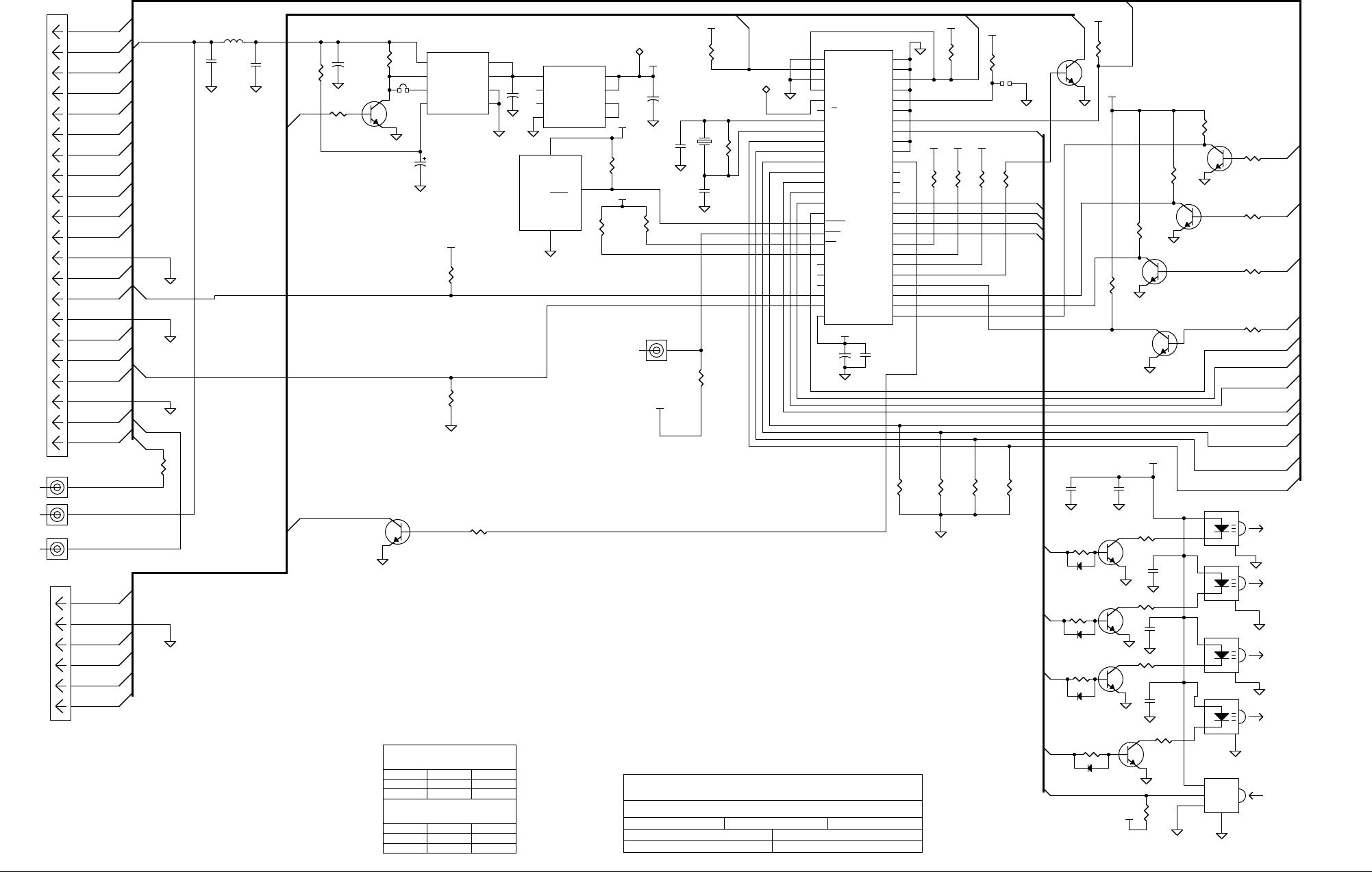
VICTORIA B.C.
DE DANIELS
ELECTRONICS
DE DANIELS
ELECTRONICS
4-19
4.5.3 OS(R/T)-3(A/H) Digital Board Schematic Diagram
DWG No: OS3150M6A
BOARD REV: 3.0
DWG REV DATE: 14 SEPT 99
C15
R41
BOARD No: 50021-03
TITLE: OS(R/T)-3(A/H) DIGITAL BOARD SCHEMATIC DIAGRAM
Enhanced AM/FM Synthesizer Instruction Manual OS(R/T)-3(A/H) 29 - 470 MHz
J4
-----
-----
JU1
JU2
Q11 U9
X1
DWN BY: STAN P
-----
-----
-----
-----
-----
-----
UNUSED REFERENCE DESIGNATORS
APRVD:DATE: 23 APRIL 1992
----- -----
HIGHEST REFERENCE DESIGNATORS
DATA OUTPUT
+12V PRG
PRIORITY COR
LOCK DETECT INPUT
POWER CONTROL
CLK
ENABLE
ACTIVE HIGH
CHAN SEL1 (I/P)
TCXO MOD INPUT
+9.5 VDC SUPPLY
MODULATION INPUT
TCXO MOD INPUT
RX MUTE
MODULATION INPUT
POWER DOWN (I/P)
TO ALL +5 VDC SUPPLY POINTS
PC7 (I/P)
PC6 (I/P)
PC5 (I/P)
PC4 (I/P)
+9.5 VDC SUPPLY
PTT (I/P) A(L)
BOOTSTRAP (I/P)
SW4 COM (O/P)
SW3 COM (O/P)
SW2 COM (O/P)
SW1 COM (O/P)
RX DATA (I/P)
TX DATA (O/P)
PTT CONTROL (O/P)
CHAN SEL0 (I/P)
CHAN SEL2 (I/P)
CHAN SEL3 (I/P)
6K81
R8 1
2
3
BC817
Q8
BC817
Q9
BC817
Q10
27K4
R27
27K4
R34
27K4
R35
27K4
R36
BC817
Q11
27K4
R22
27K4
R37
27K4
R13
100nF
C9
BC817
Q3
27K4
R2
BC817
Q1
BC817
Q2
1
2
3
BC817
Q4
BC817
Q5
BC817
Q6
ENB
CLK
DIN
LOCK
DIN
PWCTL
OUTPUT
SENSE
5VTAP
FB
INPUT
ERROR
SHDN
GND
1
2
6
74
3
5
8
U2
LP2951
P2-2
P2-1
P2-6
P2-3
P1-1
P2-4
P1-9
P1-17
VSS
MODA
AS
E
R/W
EXTAL
XTAL
PC7
PC6
PC5
PC4
PC3
PC2
PC1
PC0
RESET
XIRQ
IRQ
PD5
PD4
PD3
PD2
PD1
PD0
VDD
MODB
VRH
PE7
PE6
PE5
PE4
PE3
PE2
PE1
PE0
PB7
PB6
PB5
PB4
PB3
PB2
PB1
PB0
PA7
PA6
PA5
PA4
PA3
PA2
PA1
PA0
VRL
1
2
3
4
5
6
7
8
16
15
14
13
12
11
10
9
17
18
19
25
24
23
22
21
20
26 34
33
32
31
30
29
28
27
42
41
40
39
38
37
36
35
43
45
47
49
44
46
48
50
51
52
68HC811E2
U4
D1
D1
D2
D2
S1
G1
S2
G2
1
2
3
45
6
7
8
SI9933DY
U1
P1-12
P1-19
P1-11
P1-5
P1-13
P1-6
P1-14
P1-15
P1-8
P1-16
R14
27K4 R16
27K4 27K4
R17
DGND DGND
DGND
DGND
DGND
DGND
DGND
DGND
DGND
DGND
DGND
DGND
DGND
DGND
DGND
DGND
DGND
DGND
DGNDDGND DGND
+5VD
+5VD
+5VD
+5VD
R15
27K4
+5VD +5VD
+5VD +5VD +5VD
+5VD
DGND
+5VD
+5VD
DGND
DGND
P1-4
27K4
R5
27K4
R3
0R0
R1
27K4
R6
27K4
R4
10K0R23
10K0
R24
10K0
R25
10K0
R26
332R
R32
332R
R31
332R
R30
P1-1
P1-2
P1-4
P1-5
P1-6
P1-8
P1-9
P1-11
P1-12
P1-13
P1-14
P1-16
P1-17
P1-18
P1-19
P1-20
P1-15
C1
100nF C2
100nF
27K4
R12 27K4
R18 27K4
R19 27K4
R20
+
4.7uF
C8
+47uF
C5
TP1
+47uF
C4
IN
GND
RESET
1
2
4
MC33064
U3
DGND
10.0uH
L1
+
47uF
C3
DGND
P1-20
+5VD
P1-12B
1
2
3
4
5
6
P2
1J2
1
J1
1
2
3
4
5
6
7
8
9
10
11
12
13
14
15
16
17
18
19
20
21
P1
P1-12B
DGND
LOCK
CLK
ENB
R21
27K4
DGND
R29
27K4
R9
27K4
R28
27K4
27K4
R7
R10
27K4
2
1
8.0 Mhz
X1
R11
10M0
DGND
P2-1
P2-2
P2-3
P2-4
P2-6
1
J3
P1-18
C7
22pF
TP2
P1-2
DGND DGND
R33
332R
R38
27K4
1
J4
+5VD
27K4
R39
+5VD
DGND
PWCTL
DGND
BC817
Q7
DGND
C11
100nF C10
100nF
C12
100nF
C13
100nF
C14
100nF
DGND
DGND
C6
22pF
BAS16D1
BAS16
D2
BAS16D3
BAS16D4
+5VD 27K4
R40
JU2
DGND
221K0
R41
10uF
C15
DGND
JU1
1
2
3
OP140A
U8
DGND
1
2
3
OP140A
U7
DGND
1
2
3
OP140A
U6
DGND
1
2
3
OP140A
U5
DGND
VCC
OUT
GND
1
2
3
4
U9
OPL550
DGND
P1-17

D
EDANIELS
ELECTRONICS
4-20 Enhanced AM/FM Synthesizer Instruction Manual OS(R/T)-3(A/H) 29 - 470 MHz
This Page Intentionally Left Blank

DEDANIELS
ELECTRONICS
Enhanced AM/FM Synthesizer Instruction Manual OS(R/T)-3(A/H) 29 - 470 MHz 5-1
5 PARTS LISTS
5.1 OS(R/T)-3H 29 - 71.4 MHz Analog Board Electrical Parts List
Ref.
Desig Description Part No.
C1 - C3 CAP., SM 1.0nF CER., 0805, X7R, 50V 1008-3A102K5R
C4 CAP., SM 10nF CER, 0805, X7R, 50V 1008-4A103K5R
C5 CAP., SM 100nF CER., 0805, X7R, 50V 1008-5A104K5R
C6 CAP., SM 47uF TANT., 20%, 16V 1055-6D476M16
C7 CAP., SM 10nF CER, 0805, X7R, 50V 1008-4A103K5R
C8 CAP., SM 100nF CER., 0805, X7R, 50V 1008-5A104K5R
C9 CAP., SM 10nF CER, 0805, X7R, 50V 1008-4A103K5R
C10 CAP., SM 100nF CER., 0805, X7R, 50V 1008-5A104K5R
C11 CAP., SM 1.0uF TANT., 10%, 16V 1055-5A105M16
C12, C13 CAP., SM 4.7uF TANT., 10%, 16V 1055-5B475K16
C14 CAP., SM 10nF CER, 0805, X7R, 50V 1008-4A103K5R
C15 CAP., SM 4.7uF TANT., 10%, 16V 1055-5B475K16
C16 CAP., SM 1.0nF CER., 0805, X7R, 50V 1008-3A102K5R
C17 CAP., SM 1.0nF CER., 0805, X7R, 50V 1008-3A102K5R
C18 CAP., SM 47uF TANT., 20%, 16V 1055-6D476M16
C19 CAP., SM 10nF CER, 0805, X7R, 50V 1008-4A103K5R
C21 CAP., SM 10nF CER, 0805, X7R, 50V 1008-4A103K5R
C20 CAP., SM 4.7uF TANT., 10%, 16V 1055-5B475K16
C22 CAP., SM 10nF CER, 0805, X7R, 50V 1008-4A103K5R
C23 CAP., SM, 150pF CER., 0805,C0G 1008-2A151J1G OST-3H035
C23 CAP., SM, 100pF CER., 0805,C0G 1008-2A101J1G OST-3H045
C23 CAP., SM, 56pF CER., 0805, C0G 1008-1A560J1G OSR-3H061
C24 CAP., 1-14pF TRIM., STAND. >6 1082-A1R0014J
C25 CAP., SM 1.0nF CER., 0805, X7R, 50V 1008-3A102K5R
C26 CAP., SM 1.0nF CER., 0805, X7R, 50V 1008-3A102K5R
C27 CAP., SM 4.7uF TANT., 10%, 16V 1055-5B475K16
C28 CAP., SM 1.0nF CER., 0805, X7R, 50V 1008-3A102K5R
C29 CAP., SM 47uF TANT., 20%, 16V 1055-6D476M16
C30 CAP., SM 10nF CER, 0805, X7R, 50V 1008-4A103K5R
C31 CAP., SM 1.0nF CER., 0805, X7R, 50V 1008-3A102K5R
C32, C33 CAP., SM, 100uF TANT., 20%,16V 1055-7D107M16
C34 CAP., SM, 56pF CER., 0805, C0G 1008-1A560J1G OST-3H035
C34 CAP., SM, 47pF CER., 0805, C0G 1008-1A470J1G OST-3H045
C34 CAP., SM, 33pF CER., 0805, C0G 1008-1A330J1G OSR-3H061
C35 CAP., SM 10pF CER., 0805, COG 1008-1A100J1G
C36 CAP., SM 330pF CER., 0805, COG 1008-2A331J1G
C37, C38 CAP., 1.0uF FILM, MMK5, 10%, 63V 1016-6D105K50
C39 CAP., 1.0uF FILM, MMK5,10%,50V 1016-6D105K50
C40 CAP., SM 33pF CER., 0805, COG 1008-1A330J1G
C41 CAP., SM 1.0nF CER., 0805, X7R, 50V 1008-3A102K5R
C42 CAP., 22uF DIP. TANT., 20%, 20V 1054-6G226M20
C43 CAP., SM 10nF CER, 0805, X7R, 50V 1008-4A103K5R
C44 CAP., SM 330pF CER., 0805, COG 1008-2A331J1G
C45 CAP., 470nF FILM, MMK5,10%,63V 1016-5D474K63
C46 CAP., SM 330pF CER., 0805, COG 1008-2A331J1G
C47 CAP., SM 330pF CER., 0805, COG 1008-2A331J1G
C48 CAP., 68nF FILM, MMK5, 10%,63V 1016-4A683K63 OST-3H035

D
EDANIELS
ELECTRONICS
5-2 Enhanced AM/FM Synthesizer Instruction Manual OS(R/T)-3(A/H) 29 - 470 MHz
Ref.
Desig Description Part No.
C48 CAP., 68nF FILM, MMK5, 10%,63V 1016-4A683K63 OST-3H045
C48 CAP., Not Installed Not Installed OSR-3H061
C49 CAP., 22nF FILM, MMK5, 10%,63V 1016-4A223K63
C50 CAP., 22uF DIP. TANT., 20%, 20V 1054-6G226M20
C51 CAP., SM 10nF CER, 0805, X7R, 50V 1008-4A103K5R
C52 CAP., SM 330pF CER., 0805, COG 1008-2A331J1G
C53 CAP., SM, 56pF CER., 0805, C0G 1008-1A560J1G OST-3H035
C53 CAP., SM, 56pF CER., 0805, C0G 1008-1A560J1G OST-3H045
C53 CAP., SM, Not Installed Not Installed OSR-3H061
C54 CAP., 22uF DIP. TANT., 20%, 20V 1054-6G226M20
C55 CAP., SM 10nF CER, 0805, X7R, 50V 1008-4A103K5R
C56 CAP., SM 330pF CER., 0805, COG 1008-2A331J1G
C57 CAP., SM, 15pF CER., 0805, COG 1008-1A150J1G OST-3H035
C57 CAP., SM, 15pF CER., 0805, COG 1008-1A150J1G OST-3H045
C57 CAP., SM, 68pF CER., 0805, C0G 1008-1A680J1G OSR-3H061
C58 CAP., SM, 33pF CER., 0805, C0G 1008-1A330J1G OST-3H035
C58 CAP., SM, 33pF CER., 0805, C0G 1008-1A330J1G OST-3H045
C58 CAP., SM, 68pF CER., 0805, C0G 1008-1A680J1G OSR-3H061
C59 CAP., SM, 33pF CER., 0805, C0G 1008-1A330J1G OST-3H035
C59 CAP., SM, 33pF CER., 0805, C0G 1008-1A330J1G OST-3H045
C59 CAP., SM, 100pF CER., 0805,C0G 1008-2A101J1G OSR-3H061
C61 CAP., SM, 150pF CER., 0805,C0G 1008-2A151J1G OST-3H035
C61 CAP., SM, 100pF CER., 0805,C0G 1008-2A101J1G OST-3H045
C61 CAP., SM, 56pF CER., 0805, C0G 1008-1A560J1G OSR-3H061
C62 CAP., SM, 47pF CER., 0805, C0G 1008-1A470J1G
C63 CAP., SM, 22pF CER., 0805, C0G 1008-1A220J1G
C64 CAP., SM, 12pF CER., 0805, C0G 1008-1A120J1G
D1, D2 DIODE, MMBV609L VARICAP, SOT-23 2106-MMBV609L
D3 DIODE, MMBD701 HOT_CARR. SOT23 2105-MMBD7010
D4 DIODE, BYD17J RECTIFIER, SOD87 2101-BYD17J00
D5 DIODE, BAS16 SWITCHING, SOT23 2100-BAS16000
L1 - L4 CHOKE, RF/MOULD.10uH 10%,.25 1251-4A00100K
L5 INDUCTOR,13.5T/260nH,MOLD.,ORG 1253-A1352603 OST-3H035
L5 INDUCTOR,11.5T/197nH,MOLD.,BRN 1253-A1151971 OST-3H045
L5 INDUCTOR, 9.5T/138nH,MOLD.,WHT 1253-A0951389 OSR-3H061
L6 CHOKE, RF/MOULD.10uH 10%,.25 1251-4A00100K
L7 CHOKE, RF/MOULD.4.7uH 10%,.25 1251-TBA
L8 - L10 CHOKE, RF/MOULD.1.5uH 10%,.25 1251-3A001R5K
L11 INDUCTOR,SM,100nH CER,10%,1008 1256-2BR1000K OST-3H035
L11 INDUCTOR,SM,100nH CER,10%,1008 1256-2BR1000K OST-3H045
L11 INDUCTOR,SM,120nH CER,10%,1008 1256-2BR12OOK OSR-3H061
L12 CHOKE, RF/MOULD.,4.7uH,10%,.25 1251-3A004R7K
L13 INDUCTOR,SM,100nH CER,10%,1008 1256-2BR1000K OST-3H035
L13 INDUCTOR,SM,100nH CER,10%,1008 1256-2BR1000K OST-3H045
L13 INDUCTOR,SM,120nH CER,10%,1008 1256-2BR12OOK OSR-3H061
PCB PCB, ANALOG,OS-3H VHF 30-50MHz 4309-26500382
LED1 LED, SUB-MIN., 2mm SQ,AXIAL,ORG 2012-S229013C

DEDANIELS
ELECTRONICS
Enhanced AM/FM Synthesizer Instruction Manual OS(R/T)-3(A/H) 29 - 470 MHz 5-3
Ref.
Desig Description Part No.
Q1, Q2 TRANSISTORBC817 NPN, SOT23 2120-BC817025
Q3 TRANSISTORBC807 PNP, SOT23 2120-BC807025
Q4 TRANSISTORBC817 NPN, SOT23 2120-BC817025
Q5 JFET, J211 RF N-CHAN. TO-92 2041-J2110000
RV1 POT., SM 5K0 1T, TOP ADJ 1174-AS2502J1
R1 RES., SM 49R9 0805, 1%,100ppm 1150-1A49R9FP
R2 RES.330R METAL FILM, 5%, 0.5W 1101-2A0331JP
R3, R4 RES., SM 10K0 0805, 1%,100ppm 1150-4A1002FP
R5 RES., SM 100R 0805, 1%,100ppm 1150-2A1000FP
R6 RES., SM 1K00 0805, 1%,100ppm 1150-3A1001FP
R7, R8 RES., SM 10K0 0805, 1%,100ppm 1150-4A1002FP
R9 RES., SM 1K00 0805, 1%,100ppm 1150-3A1001FP
R10 - R12 RES., SM 10K0 0805, 1%,100ppm 1150-4A1002FP
R13 RES., SM 11K8 0805, 1%,100ppm 1150-4A1182FP
R14 RES., SM 10K0 0805, 1%,100ppm 1150-4A1002FP
R15 RES., SM 10R0 0805, 1%,100ppm 1150-1A10R0FP
R16, R17 RES., SM, 5K11 0805, 1%,100ppm 1150-3A5111FP
R18, R19 RES., SM 10K0 0805, 1%,100ppm 1150-4A1002FP
R20 RES., SM 10R0 0805, 1%,100ppm 1150-1A10R0FP
R21 RES., SM 20K0 0805, 1%,100ppm 1150-4A2002FP
R22 RES., SM, 475R 0805, 1%,100ppm 1150-2A4750FP
R23 - R25 RES., SM 10R0 0805, 1%,100ppm 1150-1A10R0FP
R26 RES.1R2 METAL FILM, 5%, 0.5W 1101-0A01R2JI
R27 RES., SM 15K0 0805, 1%,100ppm 1150-4A1502FP
R28 RES., NOT INSTALLED NOT INSTALLED
R29 RES., SM 18K2 0805, 1%,100ppm 1150-4A1822FP
R30 RES., SM 10R0 0805, 1%,100ppm 1150-1A10R0FP
R31 RES., SM 49R9 0805, 1%,100ppm 1150-1A49R9FP
R32 RES., 15K METAL FILM, 5%, 0.5W 1101-4A0153JP
R33 RES.680R METAL FILM, 5%, 0.5W 1101-2A0681JP
R34, R35 RES.10K0 METAL FILM, 5%, 0.5W 1101-4A0103JP
R36 RES., 2K7 METAL FILM, 5%, 0.5W 1101-3A0272JP
R38 RES., SM 56R2 0805, 1%,100ppm 1150-4A5622FP
R39 RES., SM 0R00 0805, ZERO OHM JUMPER 1150-0A0R0000
R40 RES.180R METAL FILM, 5%, 0.5W 1101-2A0181JP
R41 RES., SM 18R2 0805, 1%,100ppm 1150-1A18R2FP
R44 RES., SM 47R5 0805, 1%,100ppm 1150-1A47R5FP
R45 RES., SM 27R4 0805, 1%,100ppm 1150-1A27R4FP
R46 RES., SM 33R2 0805, 1%,100ppm 1150-1A33R2FP
R47 RES., SM 47R5 0805, 1%,100ppm 1150-1A47R5FP
R48 RES., SM 27R4 0805, 1%,100ppm 1150-1A27R4FP
R49 RES., SM 33R2 0805, 1%,100ppm 1150-1A33R2FP
R50 RES.180R METAL FILM, 5%, 0.5W 1101-2A0181JP
R51 RES.220R METAL FILM, 5%, 0.5W 1101-2A0221JP
R52 RES., SM 49R9 0805, 1%,100ppm 1150-1A49R9FP
R53 RES., SM 10K0 0805, 1%,100ppm 1150-4A1002FP
R54 RES., SM 18R2 0805, 1%,100ppm 1150-1A18R2FP
R55 R56 RES., SM 274 0805, 1%,100ppm 1150-2A2740FP
TCXO1 VTCXO MODULE9.6 MHz 4 PIN, +- 1ppm 2641-09600BM5

D
EDANIELS
ELECTRONICS
5-4 Enhanced AM/FM Synthesizer Instruction Manual OS(R/T)-3(A/H) 29 - 470 MHz
Ref.
Desig Description Part No.
U1 - U4 DIODE, OPL550 I/R SENSOR,TTL O/P,PLST 2014-1L18230T
U5 LED, OP140A I/R,GaAs,.81 x .23,PLAST. 2013-1G18230A
U6 I.C., LT1129-IS8, PROG. VOLT REG, SO8 2305-11290N08
U7 U8 I.C., LP2951 PROG. VOLT REG, SO-8 2305-29510N08
U9 MOSFET, SI9945DY, N CHAN.,SO-8 2142-SI9945DY
U10 I.C., MC145191, PLL FREQ/SYNTH, SO-20 2355-45191N20
U11 I.C., MSA-0611, MM1C AMP, SOT-143 2354-MSA06110
U15 U16 I.C., MSA-0611, MM1C AMP, SOT-143 2354-MSA06110

DEDANIELS
ELECTRONICS
Enhanced AM/FM Synthesizer Instruction Manual OS(R/T)-3(A/H) 29 - 470 MHz 5-5
5.2 OS(R/T)-3A 118 – 159.4 MHz Analog Board Electrical Parts List
Ref.
Desig Description Part No.
C1- C3 CAP., SM ,1.0nF CER., 0805, X7R, 50V 1008-3A102K5R
C4 CAP., SM, 10nF CER, 0805, X7R, 50V 1008-4A103K5R
C5 CAP., SM, 100nF CER., 0805, X7R, 50V 1008-5A104K5R
C6 CAP., SM, 47uF TANT., 20%, 16V 1055-6D476M16
C7 CAP., SM, 10nF CER, 0805, X7R, 50V 1008-4A103K5R
C8 CAP., SM, 100nF CER., 0805, X7R, 50V 1008-5A104K5R
C9 CAP., SM, 10nF CER, 0805, X7R, 50V 1008-4A103K5R
C10 CAP., SM, 100nF CER., 0805, X7R, 50V 1008-5A104K5R
C11 CAP., SM, 1.0uF TANT., 10%, 16V 1055-5A105M16
C12, C13 CAP., SM, 4.7uF TANT., 10%, 16V 1055-5B475K16
C14 CAP., SM, 10nF CER, 0805, X7R, 50V 1008-4A103K5R
C15 CAP., SM, 4.7uF TANT., 10%, 16V 1055-5B475K16
C16, C17 CAP., SM ,1.0nF CER., 0805, X7R, 50V 1008-3A102K5R
C18 CAP., SM, 47uF TANT., 20%, 16V 1055-6D476M16
C19 CAP., SM, 10nF CER, 0805, X7R, 50V 1008-4A103K5R
C20 CAP., SM, 4.7uF TANT., 10%, 16V 1055-5B475K16
C21, C22 CAP., SM, 10nF CER, 0805, X7R, 50V 1008-4A103K5R
C23 CAP., SM, 10pF CER., 0805, C0G 1008-1A100J1G (OST-3A128)
C23 CAP., NOT INSTALLED NOT INSTALLED (OSR-3A149)
C24 CAP., SM ,1.0nF CER., 0805, X7R, 50V 1008-3A102K5R
C25 CAP., NOT INSTALLED NOT INSTALLED
C26 CAP., SM ,1.0nF CER., 0805, X7R, 50V 1008-3A102K5R
C27 CAP., SM, 4.7uF TANT., 10%, 16V 1055-5B475K16
C28 CAP., SM, 6.8uF TANT., 20%, 10V 1055-5B685M10
C29 CAP., SM, 47uF TANT., 20%, 16V 1055-6D476M16
C30 CAP., SM, 10nF CER, 0805, X7R, 50V 1008-4A103K5R
C31 CAP., SM ,1.0nF CER., 0805, X7R, 50V 1008-3A102K5R
C32, C33 CAP., SM, 100uF TANT., 20%,16V 1055-7D107M16
C34 CAP., SM, 10nF CER, 0805, X7R, 50V 1008-4A103K5R
C35 CAP., SM, 5.6pF CER., 0805, C0G 1008-0A569D1G
C36 CAP., SM, 3.3pF CER., 0805,C0G 1008-0A339J1G
C37 CAP., 470nF FILM, MMK5,10%,63V 1016-5D474K63 (OST-3A128)
C37 CAP., 1.0uF FILM, MMK5,10%,50V 1016-6D105K50 (OSR-3A149)
C38 CAP., 100nF FILM, MMK5,10%,63V 1016-5A104K63 (OST-3A128)
C38 CAP., 1.0uF FILM, MMK5,10%,50V 1016-6D105K50 (OSR-3A149)
C39 CAP., NOT INSTALLED NOT INSTALLED (OST-3A128)
C39 CAP., 1.0uF FILM, MMK5,10%,50V 1016-6D105K50 (OSR-3A149)
C40 CAP., SM, 8.2pF CER., 0805,C0G 1008-0A829J1G (OSR-3A149)
C40 CAP., NOT INSTALLED NOT INSTALLED (OST-3A128)
C41 CAP., SM, 100nF CER., 0805, X7R, 50V 1008-5A104K5R
C42 CAP., 22uF DIP. TANT., 20%, 20V 1054-6G226M20
C43 CAP., SM, 10nF CER, 0805, X7R, 50V 1008-4A103K5R
C44 CAP., SM, 330pF CER., 0805, COG 1008-2A331J1G
C45 CAP., 470nF FILM, MMK5,10%,63V 1016-5D474K63 (OSR-3A149)
C45 CAP., 330nF FILM, MMK5,10%,50V 1016-5B334K50 (OST-3A128)
C46 CAP., SM, 10nF CER, 0805, X7R, 50V 1008-4A103K5R
C47 CAP., SM, 330pF CER., 0805, COG 1008-2A331J1G
C48 CAP., SM, 100nF CER., 0805, X7R, 50V 1008-5A104K5R
C49 CAP., 22nF FILM, MMK5, 10%,63V 1016-4A223K63 (OSR-3A149)
C49 CAP., 2.2nF FILM, MMK5,10%,63V 1016-3A222K63 (OST-3A128)

D
EDANIELS
ELECTRONICS
5-6 Enhanced AM/FM Synthesizer Instruction Manual OS(R/T)-3(A/H) 29 - 470 MHz
Ref.
Desig Description Part No.
C50, C51 CAP., SM, 100nF CER., 0805, X7R, 50V 1008-5A104K5R
C52 CAP., SM, 10nF CER, 0805, X7R, 50V 1008-4A103K5R
C53 CAP., SM, 27pF CER., 0805, COG 1008-1A270J1G
C58 CAP., SM, 47pF CER., 0805, COG 1008-1A470J1G
C59 CAP., SM, 27pF CER., 0805, COG 1008-1A270J1G
C60 CAP., SM, 2.2uF TANT., 20%, 20V 1055-5B225K20
C61 CAP., SM, 4.7uF TANT., 10%, 16V 1055-5B475K16
C62 CAP., SM, 10nF CER, 0805, X7R, 50V 1008-4A103K5R
C63 CAP., 680nF FILM, MMK5,10%,50V 1016-5D684K50
D1, D2 DIODE, MMBV609L VARICAP, SOT-23 2106-MMBV609L
D3 DIODE, MMBD701L HOT CARR., SOT23 2105-MMBD7010
D4 DIODE, BYD17J RECTIFIER, SOD87 2101-BYD17J00
D5 DIODE, BAS16 SWITCHING, SOT23 2100-BAS16000
D6, D7 DIODE, SMV1211, VARACTOR,SOT2 2106-SMV12111 (OSR-3A149)
D6 DIODE,SMV1212-4,VARACTOR,SOT23 2106-SMV12124 (OST-3A128)
D7 DIODE, SMV1211, VARACTOR,SOT2 2106-SMV12111 (OSR-3A149)
D7 DIODE, NOT INSTALLED NOT INSTALLED (OST-3A128)
L2, L3 CHOKE, RF/MOULD., 10uH 10%,.25 1251-4A00100K
L4 CHOKE, RF/MOULD., 3.9uH 10%,.25 1251-3A003R9K
L5 BOBBIN 5.5 TURNS, 1.59 mm pitch 5791-A1010300
WIRE, COPPER, 20AWG, SILVER PLD, 10.2cm 7140-30002000 (1pc 10cm, 2pcs 10mm)
L6 – L8 CHOKE, RF/MOULD., 1.5uH 10%,.25 1251-3A001R5K
L11, L12 INDUCTOR, SM, 47nH CER,10%,1008 1256-1B47N00K
L13 CHOKE, RF/MOULD., 1.5uH 10%,.25 1251-3A001R5K
LED1 LED, SUB-MIN.,2mm SQ,AXIAL,ORG 2012-S229013C
PCB PCB, ANALOG,OS-3H AM/WB SYNTH. 4309-26500825
Q1, Q2 TRANSISTOR, BC817 NPN, SOT23 2120-BC817025
Q3 TRANSISTOR, BC807 PNP, SOT23 2120-BC807025
Q4 TRANSISTOR, BC817 NPN, SOT23 2120-BC817025
Q5 JFET, J211 RF, N-CHAN., TO-92A 2041-J2110000
Q6 TRANSISTOR, MMBR901 HIGH FREQ. 2124-MMBR9010
R1 RES., SM, 49R9 0805, 1%,100ppm 1150-1A49R9FP
R2 RES., 330R METAL FILM, 5%, 0.5W 1101-2A0331JP
R3, R4 RES., SM, 10K0 0805, 1%,100ppm 1150-4A1002FP
R5 RES., SM, 100R 0805, 1%,100ppm 1150-2A1000FP
R6 RES., SM, 1K00 0805, 1%,100ppm 1150-3A1001FP
R7, R8 RES., SM, 10K0 0805, 1%,100ppm 1150-4A1002FP
R9 RES., SM, 1K00 0805, 1%,100ppm 1150-3A1001FP
R10 – R12 RES., SM, 10K0 0805, 1%,100ppm 1150-4A1002FP
R13 RES., SM, 11K8 0805, 1%,100ppm 1150-4A1182FP
R14 RES., SM, 10K0 0805, 1%,100ppm 1150-4A1002FP
R15 RES., SM, 10R0 0805, 1%,100ppm 1150-1A10R0FP
R16, R17 RES., SM, 5K11 0805, 1%,100ppm 1150-3A5111FP
R18, R19 RES., SM, 10K0 0805, 1%,100ppm 1150-4A1002FP
R20 RES., SM, 10R0 0805, 1%,100ppm 1150-1A10R0FP
R22 RES., SM, 137K0 0805, 1%,100ppm 1150-5A1373FP

DEDANIELS
ELECTRONICS
Enhanced AM/FM Synthesizer Instruction Manual OS(R/T)-3(A/H) 29 - 470 MHz 5-7
Ref.
Desig Description Part No.
R23 - R25 RES., SM, 10R0 0805, 1%,100ppm 1150-1A10R0FP
R26 RES., 1R2 METAL FILM, 5%, 0.5W 1101-0A01R2JI
R27 RES., SM, 11K8 0805, 1%,100ppm 1150-4A1182FP
R28 RES., SM, 10R0 0805, 1%,100ppm 1150-1A10R0FP
R29 RES., SM, 18K2 0805, 1%,100ppm 1150-4A1822FP
R30 RES., SM, 10R0 0805, 1%,100ppm 1150-1A10R0FP
R31 RES., SM, 100R 0805, 1%,100ppm 1150-2A1000FP
R32 RES., 15K METAL FILM, 5%, 0.5W 1101-4A0153JP (OSR-3A149)
R32 RES., 68K METAL FILM, 5%, 0.5W 1101-4A0683JP (OST-3A128)
R33 RES., 680R METAL FILM, 5%, 0.5W 1101-2A0681JP
R34, R35 RES., SM, 10K0 0805, 1%,100ppm 1150-4A1002FP
R36 RES., 1K8 METAL FILM, 5%, 0.5W 1101-3A0182JP (OSR-3A149)
R36 RES., 8K2 METAL FILM, 5%, 0.5W 1101-3A0822JP (OST-3A128)
R37, R38 RES., SM, 49K9 0805, 1%,100ppm 1150-4A4992FP
R39 RES., SM, 0R00 0805, ZERO OHM JUMPER 1150-0A0R0000
R40 RES., 330R METAL FILM, 5%,0.5W 1101-2A0391JP
R41 RES., SM, 20K0 0805, 1%,100ppm 1150-4A2002FP
R42, R43 RES., SM, 137K0 0805, 1%,100ppm 1150-5A1373FP
R44 RES., SM, 1K82 0805, 1%,100ppm 1150-3A1821FP
R45 RES., SM, 18R2 0805, 1%,100ppm 1150-1A18R2FP
R46 RES., SM, 475R0 0805, 1%,100ppm 1150-2A4750FP
R53 RES., SM, 137K0 0805, 1%,100ppm 1150-5A1373FP
R57 RES., SM, 274K 0805, 1%, 100ppm 1150-5A2743FP
R58 RES., SM, 825K0 1206, 1%,100ppm 1150-5B8253FP
R59 RES., SM, 10K0 0805, 1%,100ppm 1150-4A1002FP
R60 RES., SM, 68K1 0805, 1%,100ppm 1150-4A6812FP (OSR-3A149)
R60 RES., SM, 39K2 0805, 1%,100ppm 1150-4A3922FP (OST-3A128)
R61 RES., SM, 20K0 0805, 1%,100ppm 1150-4A2002FP
R62 RES., SM, 4K75 0805, 1%,100ppm 1150-3A4751FP
R63 RES., SM, 10R0 0805, 1%,100ppm 1150-1A10R0FP
RV1 POT., SM, 5K0 1T, TOP ADJ 1174-AS2502J1
TCXO1 VTCXO MODULE9.6 MHz 4 PIN, +- 1ppm 2641-09600BM5
U1 - U4 DIODE, OP950 I/R SENSOR,TTL O/P,PLST TBA
U5 LED, OP140A I/R,GaAs,.81 x .23,PLAST. 2013-1G18230A
U6 IC, LT1129-IS8, PROG. VOLT REG,SO-8 2305-11290N08
U7, U8 IC, LP2951 PROG. VOLT REG, SO-8 2305-29510N08
U9 MOSFET, SI9945DY, N CHAN.,SO-8 2142-SI9945DY
U10 IC, MC145190,PLL FREQ/SYNTH,SO-20 2355-45190N20
U11 IC, MSA-0611, MM1C AMP,SOT-143 2354-MSA06110
U17 IC, LTC1257I 12BIT SER.DA,S0-8 2387-12570N08
U18 IC, PIC12C672 MICROCONTROLLER, SO-8 TBA
U19 IC, MC33172 DUAL OP AMP, SO-8 2302-33172N08
U20 IC, 74HC14 HEX SCHMITT, SO-14 2376-00140N14

D
EDANIELS
ELECTRONICS
5-8 Enhanced AM/FM Synthesizer Instruction Manual OS(R/T)-3(A/H) 29 - 470 MHz
5.3 OS(R/T)-3H 128 - 174 MHz Analog Board Electrical Parts List
Ref.
Desig Description Part No.
C1-C3 CAP., SM, 1.0nF CER., 0805, X7R, 50V 1008-3A102K5R
C4 CAP., SM, 10nF CER, 0805, X7R, 50V 1008-4A103K5R
C5 CAP., SM, 100nF CER., 0805, X7R, 50V 1008-5A104K5R
C6 CAP., SM, 47µF TANT., 20%, 16V 1055-6D476M16
C7 CAP., SM, 10nF CER, 0805, X7R, 50V 1008-4A103K5R
C8 CAP., SM, 100nF CER., 0805, X7R, 50V 1008-5A104K5R
C9 CAP., SM, 10nF CER, 0805, X7R, 50V 1008-4A103K5R
C10 CAP., SM, 100nF CER., 0805, X7R, 50V 1008-5A104K5R
C11 CAP., SM, 1.0µF TANT., 10%, 16V 1055-5A105M16
C12,C13 CAP., SM, 4.7µF TANT., 10%, 16V 1055-5B475K16
C14 CAP., SM, 10nF CER, 0805, X7R, 50V 1008-4A103K5R
C15 CAP., SM, 4.7µF TANT., 10%, 16V 1055-5B475K16
C16 CAP., SM, 1.0nF CER., 0805, X7R, 50V 1008-3A102K5R
C17 CAP., SM 1.0nF CER., 0805, X7R, 50V 1008-3A102K5R
C18 CAP., SM, 47µF TANT., 20%, 16V 1055-6D476M16
C19 CAP., SM, 10nF CER, 0805, X7R, 50V 1008-4A103K5R
C20 CAP., SM, 4.7µF TANT., 10%, 16V 1055-5B475K16
C21,C22 CAP., SM, 10nF CER, 0805, X7R, 50V 1008-4A103K5R
C23 CAP., SM, 12pF CER., 0805, COG 1008-1A120J1G (OS-3H141)
C23 CAP., SM, 6.8pF CER., 0805,C0G 1008-0A689J1G (OS-3H162)
C24 CAP., TRIM., 1-14pF STAN. >6T 1082-A1R0014J
C25 CAP., SM, 1.0nF CER., 0805, X7R, 50V 1008-3A102K5R (OS-3H141)
C25 CAP., SM, 1.0nF CER., 0805, X7R, 50V 1008-3A102K5R (OS-3H162)
C26 CAP., SM, 1.0nF CER., 0805, X7R, 50V 1008-3A102K5R
C27 CAP., SM, 4.7µF TANT., 10%, 16V 1055-5B475K16
C28 CAP., SM, 6.8µF TANT., 20%, 10V 1055-5B685M10
C29 CAP., SM, 47µF TANT., 20%, 16V 1055-6D476M16
C30 CAP., SM, 10nF CER, 0805, X7R, 50V 1008-4A103K5R
C31 CAP., SM, 1.0nF CER., 0805, X7R, 50V 1008-3A102K5R
C32, C33 CAP., SM, 100uF TANT., 20%,16V 1055-7D107M16
C34 CAP., SM, 10nF CER, 0805, X7R, 50V 1008-4A103K5R
C35 CAP., SM, 3.3pF CER., 0805,C0G 1008-0A339J1G (OS-3H141)
C35 CAP., SM, 8.2pF CER., 0805,C0G 1008-0A829J1G (OS-3H162)
C36 CAP., SM, 330pF CER., 0805, COG 1008-2A331J1G
C37 CAP., 1.0µF FILM, MMK5, 10%, 50V 1016-6D105K50 (OS-3H141)
C37 CAP., 1.0µF FILM, MMK5, 10%, 50V 1016-6D105K50 (OS-3H162)
C38 CAP., 1.0µF FILM, MMK5, 10%, 50V 1016-6D105K50 (OS-3H141)
C38 CAP., 470nF FILM, MMK5,10%,63V 1016-5D474K63 (OS-3H162)
C39 CAP., 1.0µF FILM, MMK5, 10%, 63V 1016-6D105K50 (OS-3H141)
C39 CAP., NOT INSTALLED NOT INSTALLED (OS-3H162)
C40 CAP., SM, 12pF CER., 0805, C0G 1008-1A120J1G (OS-3H141)
C40 CAP., SM, 6.8pF CER., 0805,C0G 1008-0A689J1G (OS-3H162)
C42 CAP., 22µF DIP. TANT., 20%, 20V 1054-6G226M20
C43 CAP., SM, 10nF CER, 0805, X7R, 50V 1008-4A103K5R
C44 CAP., SM, 330pF CER., 0805, COG 1008-2A331J1G
C45 CAP., 470nF FILM, MMK5,10%,63V 1016-5D474K63 (OS-3H141)
C45 CAP., 220nF FILM, MMK5,10%,50V 1016-5A224K50 (OS-3H162)
C46,C47 CAP., SM, 330pF CER., 0805, COG 1008-2A331J1G
C49 CAP., 33nF FILM, MMK5, 10%, 63V 1016-4A333K63 (OS-3H141)
C49 CAP., 22nF FILM, MMK5, 10%, 63V 1016-4A223K63 (OS-3H162)

DEDANIELS
ELECTRONICS
Enhanced AM/FM Synthesizer Instruction Manual OS(R/T)-3(A/H) 29 - 470 MHz 5-9
Ref.
Desig Description Part No.
C50 CAP., 22µF DIP. TANT., 20%, 20V 1054-6G226M20
C51 CAP., SM, 10nF CER, 0805, X7R, 50V 1008-4A103K5R
C52 CAP., SM, 330pF CER., 0805, COG 1008-2A331J1G
C53 CAP., SM, 27pF CER., 0805, COG 1008-1A270J1G
C54 CAP., 22µF DIP. TANT., 20%, 20V 1054-6G226M20
C55 CAP., SM, 10nF CER, 0805, X7R, 50V 1008-4A103K5R
C56 CAP., SM, 330pF CER., 0805, COG 1008-2A331J1G
C58 CAP., SM, 47pF CER., 0805, COG 1008-1A470J1G
C59 CAP., SM, 27pF CER., 0805, COG 1008-1A270J1G
D1 DIODE, NOT INSTALLED NOT INSTALLED
D2 DIODE, MMBV609L VARICAP, SOT-23 2106-MMBV609L
D3 DIODE, MMBD701L HOT CARR., SOT23 2105-MMBD7010
D4 DIODE, BYD17J RECTIFIER,SOD87 2101-BYD17J00
D5 DIODE, BAS16 SWITCHING, SOT23 2100-BAS16000
L1-L3 CHOKE, RF/MOULD., 10uH 10%,.25 1251-4A00100K
L4 CHOKE, RF/MOULD., 1.5uH 10%,.25 1251-3A001R5K
L5 BOBBIN, 5.5 TURNS, 1.59 mm pitch 5791-A1010300
WIRE, COPPER, 20AWG, Ag PLATED, 11cm 7140-30002000 (1pc 9cm, 2pcs 1cm)
L6-L10 CHOKE, RF/MOULD., 1.5uH 10%,.25 1251-3A001R5K
L11,L12 INDUCTOR, SM, 47nH CER,10%,1008 1256-1B47N00K
L12 INDUCTOR, SM, 47nH CER,10%,1008 1256-1B47N00K
LED1 LED, SUB-MIN.,2mm SQ,AXIAL,ORG 2012-S229013C
PCB PCB, ANALOG, OS-3H H/P SYNTH. 4309-26500252
Q1,Q2 TRANSISTOR, BC817-25,NPN,SOT23 2120-BC817025
Q3 TRANSISTOR, BC807 PNP, SOT23 2120-BC807025
Q4 TRANSISTOR, BC817 NPN, SOT23 2120-BC817025
Q5 JFET, J211 RF, N-CHAN., TO-92A 2041-J2110000
R1 RES., SM, 49R9 0805, 1%,100ppm 1150-1A49R9FP
R2 RES., 330R METAL FILM, 5%, 0.5W 1101-2A0331JP
R3,R4 RES., SM, 10K0 0805, 1%,100ppm 1150-4A1002FP
R5 RES., SM, 100R 0805, 1%,100ppm 1150-2A1000FP
R6 RES., SM, 1K00 0805, 1%,100ppm 1150-3A1001FP
R7,R8 RES., SM, 10K0 0805, 1%,100ppm 1150-4A1002FP
R9 RES., SM, 1K00 0805, 1%,100ppm 1150-3A1001FP
R10-R12 RES., SM, 10K0 0805, 1%,100ppm 1150-4A1002FP
R13 RES., SM, 11K8 0805, 1%,100ppm 1150-4A1182FP
R14 RES., SM, 10K0 0805, 1%,100ppm 1150-4A1002FP
R15 RES., SM, 10R0 0805, 1%,100ppm 1150-1A10R0FP
R16, R17 RES., SM, 5K11 0805, 1%,100ppm 1150-3A5111FP
R18, R19 RES., SM, 10K0 0805, 1%,100ppm 1150-4A1002FP
R20 RES., SM, 10R0 0805, 1%,100ppm 1150-1A10R0FP
R21 RES., SM, 20K0 0805, 1%,100ppm 1150-4A2002FP
R22 RES., SM, 100R 0805, 1%,100ppm 1150-2A1000FP
R23-R25 RES., SM, 10R0 0805, 1%,100ppm 1150-1A10R0FP
R26 RES., 1R2 METAL FILM, 5%, 0.5W 1101-0A01R2JI
R27 RES., SM, 11K8 0805, 1%,100ppm 1150-4A1182FP

D
EDANIELS
ELECTRONICS
5-10 Enhanced AM/FM Synthesizer Instruction Manual OS(R/T)-3(A/H) 29 - 470 MHz
Ref.
Desig Description Part No.
R28 RES., NOT INSTALLED NOT INSTALLED
R29 RES., SM, 18K2 0805, 1%,100ppm 1150-4A1822FP
R30 RES., SM, 10R0 0805, 1%,100ppm 1150-1A10R0FP
R31 RES., SM, 49R9 0805, 1%,100ppm 1150-1A49R9FP
R32 RES., 12K METAL FILM, 5%, 0.5W 1101-4A0123JP (OS-3H141)
R32 RES., 15K METAL FILM, 5%, 0.5W 1101-4A0153JP (OS-3H162)
R33 RES., 680R METAL FILM, 5%, 0.5W 1101-2A0681JP
R34,R35 RES., SM, 10K0 0805, 1%,100ppm 1150-4A1002FP
R36 RES., 2K2 METAL FILM, 5%, 0.5W 1101-3A0222JP (OS-3H141)
R36 RES., 6K2 METAL FILM, 5%, 0.5W 1101-3A0622JP (OS-3H162)
R39 RES., SM, 0 0805, ZERO OHM JUMPER 1150-0A0R0000
R40 RES., 180R METAL FILM, 5%, 0.5W 1101-2A0181JP
R41 RES., SM, 18R2 0805, 1%,100ppm 1150-1A18R2FP
R44 RES., SM, 47R5 0805, 1%,100ppm 1150-1A47R5FP
R45 RES., SM, 27R4 0805, 1%,100ppm 1150-1A27R4FP
R46 RES., SM, 33R2 0805, 1%,100ppm 1150-1A33R2FP
R47 RES., SM, 47R5 0805, 1%,100ppm 1150-1A47R5FP
R48 RES., SM, 47R5 0805, 1%,100ppm 1150-1A47R5FP
R49 RES., SM, 10R0 0805, 1%,100ppm 1150-1A10R0FP
R50 RES., 180R METAL FILM, 5%, 0.5W 1101-2A0181JP
R51 RES., 220R METAL FILM, 5%, 0.5W 1101-2A0221JP
R52 RES., SM, NOT INSTALLED. NOT INSTALLED
R53 RES., SM, 10K0 0805, 1%,100ppm 1150-4A1002FP
R54 RES., SM, 18R2 0805, 1%,100ppm 1150-1A18R2FP
R55 RES., SM, 274 0805, 1%,100ppm 1150-2A2740FP
R56 RES., SM, 274 0805, 1%,100ppm 1150-2A2740FP
RV1 POT., SM, 5K0 1T, TOP ADJ 1174-AS2502J1
TCXO1 VTCXO MODULE, 9.6 MHz 4 PIN, +- 1ppm 2641-09600BM5
U1-U4 DIODE, I/R SENSOR,TTL O/P,PLST 2014-1L18230T
U5 LED, I/R,GaAs,.81 x .23,PLAST. 2013-1G18230A
U6 I.C., LT1129-IS8 ,PROG. VOLT REG,SO8 2305-11290N08
U7,U8 I.C., LP2951 PROG. VOLT REG, SO-8 2305-29510N08
U9 MOSFET, SI9945DY, N CHAN.,SO-8 2142-SI9945DY
U10 IC, 45191,PLL FREQ/SYNTH,SO-20 2355-45191N20
U11 IC, MSA-0611, MM1C AMP,SOT-143 2354-MSA06110
U15,U16 IC, MSA-0611, MM1C AMP,SOT-143 2354-MSA06110

DEDANIELS
ELECTRONICS
Enhanced AM/FM Synthesizer Instruction Manual OS(R/T)-3(A/H) 29 - 470 MHz 5-11
5.4 OS(R/T)-3H 406 - 470 MHz Analog Board Electrical Parts List
Ref.
Desig Description Part No.
C1 - C3 CAP., SM 1.0nF CER., 0805, X7R, 50V 1008-3A102K5R
C4 CAP., SM 10nF CER, 0805, X7R, 50V 1008-4A103K5R
C5 CAP., SM 100nF CER., 0805, X7R, 50V 1008-5A104K5R
C6 CAP., SM 47uF TANT., 20%, 16V 1055-6D476M16
C7 CAP., SM 10nF CER, 0805, X7R, 50V 1008-4A103K5R
C8 CAP., SM 100nF CER., 0805, X7R, 50V 1008-5A104K5R
C9 CAP., SM 10nF CER, 0805, X7R, 50V 1008-4A103K5R
C10 CAP., SM 100nF CER., 0805, X7R, 50V 1008-5A104K5R
C11 CAP., SM 1.0uF TANT., 10%, 16V 1055-5A105M16
C12, C13 CAP., SM 4.7uF TANT., 10%, 16V 1055-5B475K16
C14 CAP., SM 10nF CER, 0805, X7R, 50V 1008-4A103K5R
C15 CAP., SM 4.7uF TANT., 10%, 16V 1055-5B475K16
C16 CAP., 100nF FILM, MMK5, 10%, 63V 1016-5A104K63
C17 CAP., SM 1.0nF CER., 0805, X7R, 50V 1008-3A102K5R
C18 CAP., SM 47uF TANT., 20%, 16V 1055-6D476M16
C19 CAP., SM 10nF CER, 0805, X7R, 50V 1008-4A103K5R
C20 CAP., SM 4.7uF TANT., 10%, 16V 1055-5B475K16
C21, C22 CAP., SM 10nF CER, 0805, X7R, 50V 1008-4A103K5R
C25, C26 CAP., SM 1.0nF CER., 0805, X7R, 50V 1008-3A102K5R
C27 CAP., SM 4.7uF TANT., 10%, 16V 1055-5B475K16
C29 CAP., SM 47uF TANT., 20%, 16V 1055-6D476M16
C30 CAP., SM 10nF CER, 0805, X7R, 50V 1008-4A103K5R
C31 CAP., SM 1.0nF CER., 0805, X7R, 50V 1008-3A102K5R
C32, C33 CAP., SM, 100uF TANT., 20%,16V 1055-7D107M16
C34 CAP., SM 10nF CER, 0805, X7R, 50V 1008-4A103K5R
C35 CAP., SM 100pF CER., 0805, COG 1008-2A101J1G
C36 CAP., SM 330pF CER., 0805, COG 1008-2A331J1G
C37 CAP., 1.0uF FILM, MMK5,10%,50V 1016-6D105K50
C38 CAP., NOT INSTALLED NOT INSTALLED OST-3H440
C38 CAP., 1.0uF FILM, MMK5,10%,50V 1016-6D105K50 OSR-3H440
C39 CAP., NOT INSTALLED NOT INSTALLED OST-3H440
C39 CAP., 1.0uF FILM, MMK5,10%,50V 1016-6D105K50 OSR-3H440
C42 CAP., 22uF DIP. TANT., 20%, 20V 1054-6G226M20
C43 CAP., SM 10nF CER, 0805, X7R, 50V 1008-4A103K5R
C44 CAP., SM 330pF CER., 0805, COG 1008-2A331J1G
C45 CAP., 220nF FILM, MMK5,10%,50V 1016-5A224K50 OST-3H440
C45 CAP., 470nF FILM, MMK5,10%,50V 1016-5C474K50 OSR-3H440
C46 CAP., SM 330pF CER., 0805, COG 1008-2A331J1G
C47 CAP., SM 330pF CER., 0805, COG 1008-2A331J1G
C49 CAP., 22nF FILM, MMK5, 10%,63V 1016-4A223K63 OST-3H440
C49 CAP., 33nF FILM, MMK5, 10%,63V 1016-4A333K63 OSR-3H440
C50 CAP., 22uF DIP. TANT., 20%, 20V 1054-6G226M20
C51 CAP., SM 10nF CER, 0805, X7R, 50V 1008-4A103K5R
C52 CAP., SM 330pF CER., 0805, COG 1008-2A331J1G
C53 CAP., SM, 10pF CER., 0805, C0G 1008-1A100J1G
C54 CAP., 22uF DIP. TANT., 20%, 20V 1054-6G226M20
C55 CAP., SM 10nF CER, 0805, X7R, 50V 1008-4A103K5R
C56 CAP., SM 330pF CER., 0805, COG 1008-2A331J1G
C58 CAP., SM, 15pF CER., 0805, C0G 1008-1A150J1G
C59 CAP., SM, 10pF CER., 0805, C0G 1008-1A100J1G

D
EDANIELS
ELECTRONICS
5-12 Enhanced AM/FM Synthesizer Instruction Manual OS(R/T)-3(A/H) 29 - 470 MHz
Ref.
Desig Description Part No.
C60 CAP., 100nF FILM, MMK5, 10%, 63V 1016-5A104K63 OST-3H440
C60 CAP., NOT INSTALLED NOT INSTALLED OSR-3H440
D4 DIODE, BYD17J RECTIFIER,SOD87 2101-BYD17J00
D5 DIODE, BAS16 SWITCHING, SOT23 2100-BAS16000
L1 - L3 CHOKE, RF/MOULD.10uH 10%,.25 1251-4A00100K
L6 - L10 CHOKE, RF/MOULD.1.5uH 10%,.25 1251-3A001R5K
L11 L12 INDUCTOR, SM18nH CER,10%,1008 1256-1B18N00K
LED1 LED, SUB-MIN.,2mm SQ,AXIAL,ORG 2012-S229013C
PCB PCB, ANALOG, OS-3H UHF SYNTH. 4309-27500282
Q1, Q2 TRANSISTOR, BC817 NPN, SOT23 2120-BC817025
Q3 TRANSISTOR, BC807 PNP, SOT23 2120-BC807025
Q4 TRANSISTOR, BC817 NPN, SOT23 2120-BC817025
R1 RES., SM 49R9 0805, 1%,100ppm 1150-1A49R9FP
R2 RES.330R METAL FILM, 5%, 0.5W 1101-2A0331JP
R3 R4 RES., SM 10K0 0805, 1%,100ppm 1150-4A1002FP
R5 RES., SM 100R 0805, 1%,100ppm 1150-2A1000FP
R6 RES., SM 1K00 0805, 1%,100ppm 1150-3A1001FP
R7 R8 RES., SM 10K0 0805, 1%,100ppm 1150-4A1002FP
R9 RES., SM 1K00 0805, 1%,100ppm 1150-3A1001FP
R10 - R12 RES., SM 10K0 0805, 1%,100ppm 1150-4A1002FP
R13 RES., SM 11K8 0805, 1%,100ppm 1150-4A1182FP
R14 RES., SM 10K0 0805, 1%,100ppm 1150-4A1002FP
R15 RES., SM 10R0 0805, 1%,100ppm 1150-1A10R0FP
R16, R17 RES., SM, 5K11 0805, 1%,100ppm 1150-3A5111FP
R18, R19 RES., SM 10K0 0805, 1%,100ppm 1150-4A1002FP
R21 RES., 2K7 METAL FILM, 5%, 0.5W 1101-3A0272JP OST-3H440
R21 RES., NOT INSTALLED NOT INSTALLED OSR-3H440
R23 RES., SM 10R0 0805, 1%,100ppm 1150-1A10R0FP
R24, R25 RES., SM 10R0 0805, 1%,100ppm 1150-1A10R0FP
R26 RES.1R2 METAL FILM, 5%, 0.5W 1101-0A01R2JI
R28 RES., SM 10R0 0805, 1%,100ppm 1150-1A10R0FP
R29 RES., SM 36K5 0805, 1%,100ppm 1150-4A3652FP
R30 RES., SM 10R0 0805, 1%,100ppm 1150-1A10R0FP
R31 RES., SM 274R 0805, 1%,100ppm 1150-2A2740FP
R32 RES., 4K7 METAL FILM, 5%, 0.5W 1101-3A0472JP OSR-3H440
R32 RES., 5K6 METAL FILM, 5%, 0.5W 1101-3A0562JP OST-3H440
R33 RES.680R METAL FILM, 5%, 0.5W 1101-2A0681JP
R34, R35 RES., SM 10K0 0805, 1%,100ppm 1150-4A1002FP
R36 RES., 2K2 METAL FILM, 5%, 0.5W 1101-3A0222JP OST-3H440
R36 RES., 1K5 METAL FILM, 5%, 0.5W 1101-3A0152JP OSR-3H440
R39 RES., SM 0R0 0805, ZERO OHM JUMPER 1150-0A0R0000
R40 RES.180R METAL FILM, 5%, 0.5W 1101-2A0181JP
R41 RES., SM 18R2 0805, 1%,100ppm 1150-1A18R2FP
R44 RES., SM 47R5 0805, 1%,100ppm 1150-1A47R5FP
R45 RES., SM 27R4 0805, 1%,100ppm 1150-1A27R4FP
R46 RES., SM 33R2 0805, 1%,100ppm 1150-1A33R2FP

DEDANIELS
ELECTRONICS
Enhanced AM/FM Synthesizer Instruction Manual OS(R/T)-3(A/H) 29 - 470 MHz 5-13
Ref.
Desig Description Part No.
R47 RES., SM 47R5 0805, 1%,100ppm 1150-1A47R5FP
R48 RES., SM 27R4 0805, 1%,100ppm 1150-1A27R4FP
R49 RES., SM 33R2 0805, 1%,100ppm 1150-1A33R2FP
R50 RES.180R METAL FILM, 5%, 0.5W 1101-2A0181JP
R51 RES.220R METAL FILM, 5%, 0.5W 1101-2A0221JP
R52 RES., SM 49R9 0805, 1%,100ppm 1150-1A49R9FP
R53 RES., SM 10K0 0805, 1%,100ppm 1150-4A1002FP
R54 RES., SM 18R2 0805, 1%,100ppm 1150-1A18R2FP
R55, R56 RES., SM 274R 0805, 1%,100ppm 1150-2A2740FP
R57 RES., SM 18R2 0805, 1%,100ppm 1150-1A18R2FP
R58 RES., SM 274R 0805, 1%,100ppm 1150-2A2740FP
RV1 POT., SM5K0 1T, TOP ADJ 1174-AS2502J1
TCXO1 VTCXO MODULE 9.6 MHz 4 PIN, +- 1ppm 2641-09600BM5
U1 - U4 DIODE, OPL550 I/R SENSOR,TTL O/P,PLST 2014-1L18230T
U5 LED, OP140A I/R,GaAs,.81 x .23,PLAST. 2013-1G18230A
U6 I.C., LT1129-IS8,PROG. VOLT REG, SO8 2305-11290N08
U7, U8 I.C.LP2951 PROG. VOLT REG, SO-8 2305-29510N08
U9 MOSFET, SI9945DY, N CHAN.,SO-8 2142-SI9945DY
U10 I.C., MC14519, PLL FREQ/SYNTH, SO-20 2355-45190N20
U11 I.C., MSA-0611, MM1C AMP, SOT-143 2354-MSA06110
U15, U16 I.C., MSA-0611, MM1C AMP, SOT-143 2354-MSA06110
U17 VCO MODULE,427.4-451.4MHz,T-PK 2621-L002309T OSR-3H440
U17 VCO MODULE, 406-470 MHz,T-PKG. 2621-190435MT OST-3H440

D
EDANIELS
ELECTRONICS
5-14 Enhanced AM/FM Synthesizer Instruction Manual OS(R/T)-3(A/H) 29 - 470 MHz
5.5 OS(R/T)-3(A/H) Digital Board Electrical Parts List
Ref.
Desig Description Part No.
C1,C2 CAP., SM, 100nF CER., 0805, X7R, 50V 1008-5A104K5R
C3-C5 CAP., SM, 47µF TANT., 20%, 16V 1055-6D476M16
C6,C7 CAP., SM, 22pF CER., 0805, COG 1008-1A220J1G
C8 CAP., SM, 4.7µF TANT., 10%, 16V 1055-5B475K16
C9-C14 CAP., SM, 100nF CER., 0805, X7R, 50V 1008-5A104K5R
C15 CAP., SM, 10µF TANT., 20%, 16V 1055-6C106M16
P1 INTERCONNECT/STD,1ROW x 12P,Au 5015-IS112G21
INTERCONNECT/STD,1ROW x9PIN,Au 5015-IS109G21
P2 INTERCONNECT/STD,1ROW x6PIN,Au 5015-IS106G21
D1 - D4 DIODE, BAS16 SWITCHING, SOT23 2100-BAS16000
L1 INDUCTOR, SM, 10.0uH, 10%,1812 1255-4G10000K
PCB PCB, DIGITAL, OS-3H H/P SYNTH. 4309-26500213
Q1 - Q11 TRANSISTOR, BC817-25,NPN,SOT23 2120-BC817025
R1 RES., SM, 0 0805, ZERO OHM JUMPER 1150-0A0R0000
R2-R7 RES., SM, 47K5 0805, 1%,100ppm 1150-4A4752FP
R8 RES., SM, 6K81 0805, 1%,100ppm 1150-3A6811FP
R9,R10 RES., SM, 47K5 0805, 1%,100ppm 1150-4A4752FP
R11 RES., SM, 10M0 1206, 5%,400ppm 1151-7B0106JG
R12-R22 RES., SM, 47K5 0805, 1%,100ppm 1150-4A4752FP
R23-R26 RES., SM, 10K0 0805, 1%,100ppm 1150-4A1002FP
R27-R29 RES., SM, 47K5 0805, 1%,100ppm 1150-4A4752FP
R30-R33 RES., SM, 332R 0805, 1%,100ppm 1150-2A3320FP
R34-R40 RES., SM, 47K5 0805, 1%,100ppm 1150-4A4752FP
R41 RES., SM, 221K 0805, 1%, 100ppm 1150-5A2213FP
U1 MOSFET, SI9933DY, P CHAN.,SO-8 2142-SI9933DY
U2 IC, LP2951,PROG. VOLT REG,SO-8 2305-29510N08
U3 IC, MC33064,UNDR/VOLT SEN.SO-8 2308-33064N08
U4 IC, 68HC811E2, MIC/CTR, PLCC52 2380-68811P52
U5-U8 LED, I/R,GaAs,.81 x .23,PLAST. 2013-1G18230A
U9 DIODE, I/R SENSOR,TTL O/P,PLST 2014-1L18230T
X1 RESONATOR, SM, 8.0MHz, CERAMIC 1575-8001816A

DEDANIELS
ELECTRONICS
Enhanced AM/FM Synthesizer Instruction Manual OS(R/T)-3(A/H) 29 - 470 MHz 5-15
5.6 OS(R/T)-3(A/H) Synthesizer Mechanical Parts List
Description Part No. Qty.
CASE, OS-3H SYNTH. MODULE,ALUM 3702-66100920 1
CONN., SMB, JACK,2 HOLE FLANGE 5120-J2SC01BG 2
FERRITE, BEAD,73 MIX, 3X3.5mm OD (CON3-CON5) 1210-73030350 3 OS-3H050
FERRITE, BEAD,43 MIX, 3X3.5mm OD (CON3-CON5) 1210-43030350 3 OS-3A130
FERRITE, BEAD,43 MIX, 3X3.5mm OD (CON3-CON5) 1210-43030350 3 OS-3H150
FERRITE, BEAD,61 MIX, 3X3.5mm OD (CON3-CON5) 1210-61030350 3 OS-3H440
HEADER, .1”, 1 ROWX3PIN, AU 5010-H103ST7L 2
LABEL, FOIL,FRQ/SN,OS-3H SYNTH 3501-13091006 1
LID, CASE,OS-3H SYNTH/MODL.,AL 3702-66100921 1
PIN, 2 x 10mm, GROOVED W/PILOT 5876-D1470210 4
SCREW, M2.0 x 4, FLAT/PHIL, A2 5812-2M0FP04S 8
SCREW, M2 X 4, PAN/PHILLIPS,A2 5812-2M0PP04S 15
SCREW, M2.5 x 24.5 FLAT/PHIL, A2 5812-2M5FP24S 1
WASHER, TFE,0.036ID,1/8OD,.02T 5805-T3612F20 6

D
EDANIELS
ELECTRONICS
5-16 Enhanced AM/FM Synthesizer Instruction Manual OS(R/T)-3(A/H) 29 - 470 MHz
This Page Intentionally Left Blank

DEDANIELS
ELECTRONICS
Enhanced AM/FM Synthesizer Instruction Manual OS(R/T)-3(A/H) 29 - 470 MHz 6-1
6 REVISION HISTORY
ISSUE
DATE
REVISION
1 May 97 • Issue 1
2 Mar 98 • Changes to the AM Analog board (OST-3A128) to improve performance
ECO #547.
C37 was 220nF is now 100nF and C40 was 8.2pF is now not installed
C45 was 33nF is now 22nF and C49 was 2.2nF is now 1.5nF
R32 was 33kΩ is now 56kΩand R36 was 3k3Ω is now 5k6Ω
3 Mar 00 • Changes to the AM Analog board to improve performance at -40˚C.
ECO #565.
L4 was 1.5µH is now 3.9 µH
• Changes to the FM Analog boards to improve manufacturing. ECO #572
C32 & C33 were 100µF through hole tantalums are now 100µF surface
mount tantalums
• Changes to the OS-3A/H Digital board for compatibility with the new AM
wideband Synthesizers. ECO #579.
Added C15 (10µF) and R41 (221kΩ).
JU1 was added and is installed for AM modules only.
PCB, DIGITAL, OS-3H/P SYNTH was version 2 now version 3.
• Added the new component layouts, schematic diagram and parts lists for
the new AM wideband synthesizer. Wideband referring to only having to
be tune once and working over the whole AM band (118-138 MHz).

DE DANIELS
ELECTRONICS
6-2 Enhanced AM/FM Synthesizer Instruction Manual OS(R/T)-3(A/H) 29 - 470 MHz
ISSUE
DATE
REVISION