Digi 50M1699 WLAN Module User Manual CC Wi i MX51 HRM
Digi International Inc WLAN Module CC Wi i MX51 HRM
Digi >
Contents
- 1. User Manual Part1
- 2. User Manual Part2
- 3. User Manual Part3
- 4. User Manual Part4
- 5. User Manual
User Manual Part1

ConnectCore TM for i.MX51TM
Hardware Reference
Preliminary Information
90001128_D
12/22/2010
©2010DigiInternational,Inc. 2
©2010 Digi International Inc.
All rights reserved.
Digi, Digi International, the Digi logo, a Digi International Company, Digi JumpStart Kit, ConnectCore, NET+,
NET+OS and NET+Works are trademarks or registered trademarks of Digi International, Inc. in the United States
and other countries worldwide. All other trademarks are the property of their respective owners.
All other trademarks mentioned in this document are the property of their respective owners.
Information in this document is subject to change without notice and does not represent a commitment on the
part of Digi International.
Digi provides this document “as is,” without warranty of any kind, either expressed or implied, including, but
not limited to, the implied warranties of fitness or merchantability for a particular purpose. Digi may make
improvements and/or changes in this manual or in the product(s) and/or the program(s) described in this manual
at any time.
This product could include technical inaccuracies or typographical errors. Changes are periodically made to the
information herein; these changes may be incorporated in new editions of the publication.
Contents
©2010DigiInternational,Inc. 3
Chapter 1: About the Module........................................... 9
Features and Functionality ..................................................10
Module Variant ...............................................................11
Block Diagram .................................................................12
CPU............................................................................ 12
Module ........................................................................ 13
Module Pinout .................................................................14
Pinout Legend ................................................................14
J1 Pinout ..................................................................... 14
J2 Pinout ..................................................................... 21
Power ...........................................................................30
Module Power Supplies..................................................... 30
Supply Inputs................................................................. 30
Supply Outputs .............................................................. 31
MC13892 Power Management ..............................................32
Memory .........................................................................33
DDR2 SDRAM Memory ....................................................... 33
NAND Flash Memory......................................................... 33
Chip selects ....................................................................33
Chip Select Memory Map................................................... 33
Multiplexed GPIO .............................................................34
GPIO Multiplexing Table ....................................................34
Interfaces ......................................................................39
1-Wire .........................................................................39
Accelerometer ...............................................................39
ADC and Touch Screen ..................................................... 39
Synchronous Serial Interface (SSI) ........................................40
External Memory Interface (EMI) .........................................41
Ethernet 1 ....................................................................41
Ethernet 2 ....................................................................41
I2C .............................................................................42
Video Subsystem ............................................................ 43
Video Processing Unit (VPU)............................................... 43
Image Processing Unit (IPU) ............................................... 45
Keypad ........................................................................47
Memory Cards................................................................ 47
PWM ...........................................................................48
RTC............................................................................ 49
SPDIF ..........................................................................49
SPI .............................................................................50
Contents
©2010DigiInternational,Inc. 4
Watchdog Timer .............................................................50
UART .......................................................................... 51
USB Host and USB OTG .....................................................51
WLAN ...........................................................................52
WLAN ..........................................................................52
Cable Specification: U.FL/W.FL to RP-SMA .............................53
Chapter 2: About the Development Board ..................... 54
What’s on the Development Board? ........................................54
The Development Board ....................................................56
Switches and Push-buttons ..................................................57
Power Switch, S2 ............................................................57
Reset Button, S4 .............................................................58
Power Button, S11 ..........................................................58
User Buttons, S3 and S5.................................................... 58
Ident Button, S10 ........................................................... 58
Legend for Multi-Position Switches....................................... 58
UART 1 Switch, S6........................................................... 59
UART 2 Switch, S7........................................................... 59
Boot Configuration Switches, S8 and S9 .................................60
Jumpers ........................................................................ 61
Battery Enable, J5 .......................................................... 61
Module Power Source, P29 .................................................62
LED 1, J16 .................................................................... 62
LED 2, J9 ......................................................................62
Button 1, J28 .................................................................62
Button 2, J29 .................................................................62
UART3 / XBee Selection, J30 and J31 ....................................62
WLAN Disable, J17 ..........................................................62
Touch Selection, J20 ....................................................... 62
Coincell Enable, J3 ......................................................... 63
JTAG Mod., J4 ............................................................... 63
LEDs .............................................................................64
WLAN, LE12 ..................................................................64
WLAN, LE12 .................................................................. 65
Power LEDs, LE3, LE4, LE6 and LE7 ........................................65
User LEDs, LE49 and LE51.................................................. 65
Serial Status LEDs ........................................................... 65
UART 1 Status LEDs ......................................................... 66
UART 2 Status LEDs ......................................................... 66
Contents
©2010DigiInternational,Inc. 5
XBee Assoc., LE50 ...........................................................66
Audio Interface ............................................................... 67
Line-out Connector Pinout, J18 ...........................................68
Line-in Connector Pinout, J12 ............................................ 68
Microphone Connector Pinou, J15t....................................... 68
Coin Cell Battery.............................................................. 69
Camera Interfaces ............................................................70
X15 Pinout ....................................................................71
X17 Pinout.................................................................... 71
Digital IO Interface............................................................72
Digital I/O Connector, X45 .................................................73
Ethernet 1 Interface ......................................................... 74
Ethernet 1, RJ-45 Connector X7 .......................................... 75
Ethernet 2 Interface ......................................................... 76
Ethernet 2, Connector J17 .................................................77
HDMI Interface ................................................................ 78
HDMI Connector, J19 .......................................................79
I2C Interface ...................................................................80
2C Header, P22 ..............................................................81
JTAG Interface ................................................................82
Standard JTAG ARM Connector, X13 .....................................83
LCD Interfaces .................................................................84
LCD 1 Connector, P1 ........................................................85
P1 Pinout ..................................................................... 85
LCD 2 Connector, P2 ........................................................87
P2 Pinout ..................................................................... 87
MicroSD™ Card Interface..................................................... 89
MicroSD™ Connector, X14.................................................. 90
Module Connectors and Signal Rails ........................................91
Module Connectors ..........................................................92
Signal Rails, J25 and J26 ...................................................92
J25 Pinout ....................................................................92
J26 Pinout ....................................................................95
Peripheral Application Header ..............................................98
Peripheral Application Header, P21...................................... 99
Power-Over-Ethernet (PoE) - IEEE802.3af ............................... 101
The PoE Module ............................................................ 102
PoE Connector (power in), P17 .......................................... 102
PoE Connector (power out), P18 ........................................ 103
Main Power Connector ..................................................... 104
SD-Card Interface ........................................................... 105
Contents
©2010DigiInternational,Inc. 6
SD/MMC Connector, X18 .................................................. 106
SPI Interface ................................................................. 107
SPI Header, P24 ............................................................ 108
UART Interface .............................................................. 109
Serial Port 2, RS232, X27 ................................................. 109
Serial Port 1, MEI Interface, X30......................................... 110
Serial Port 3, TTL Interface, X19 ....................................... 111
USB Host Interface .......................................................... 112
USB Host Connectors, J8 and J10 ....................................... 112
USB OTG Interface........................................................... 113
USB OTG Connector, J11.................................................. 113
User Interface ............................................................... 114
Analog Video Interface ..................................................... 116
Analog Video Connector, X32 ............................................ 117
WLAN Interface .............................................................. 118
Antenna Connectors (WLAN) ............................................. 119
Digi XBee TM Interface...................................................... 120
Digi XBeeTM Module Connectors, X28 and X29 ....................... 121
Appendix A: Module Specifications ..... 122
Mechanical Specifications ................................................. 123
Environmental Specifications ............................................. 123
Network Interface .......................................................... 124
Antenna specifications: 802.11 a/b/g antenna ....................... 124
Antenna Specification: 802.11b/g antenna ............................ 125
Ethernet 1 .................................................................. 126
Ethernet 2................................................................... 126
WLAN ........................................................................ 127
Electrical Characteristics .................................................. 130
Supply Voltages............................................................. 130
Supply Current ............................................................. 130
On-Module Power Supplies................................................ 133
I/O DC Parameters......................................................... 133
Appendix B: Module Dimensions ......... 140
Top View .................................................................... 141
Bottom View ................................................................ 142
Side View.................................................................... 143
Connectors ................................................................. 143
Contents
©2010DigiInternational,Inc. 7
Appendix C: Certifications ................ 144
FCC Part 15 Class B.......................................................... 144
Radio Frequency Interface (RFI) (FCC 15.105) ........................ 144
Labeling Requirements (FCC 15.19)..................................... 144
RF Exposure................................................................. 145
Modifications (FCC 15.21)................................................. 145
Industry Canada ............................................................ 145
Indoor/Outdoor ............................................................ 146
Declaration of Conformity ............................................... 146
International EMC Standards ............................................. 147
Appendix D: Change Log ................... 148
Revision A..................................................................... 148
Revision B .................................................................... 148
Revision C .................................................................... 148
Revision D..................................................................... 148

©2010DigiInternational,Inc. 8
Using this Guide
This guide provides information about the Digi ConnectCore for i.MX51 embedded
core module family.
Conventions used in this guide
This table describes the typographic conventions used in this guide:
Digi Information
Document Updates
Please always check the product specific section on the Digi support website at
www.digiembedded.com/support for the most current revision of this document.
Contact Information
For more information about your Digi products, or for customer service and
technical support, contact Digi International.
Additional Resources
Please also refer to the most recent Freescale i.MX51 processor reference manual
and related documentation for additional information.
This convention Is used for
italic type Emphasis, new terms, variables, and document titles.
monospaced type Filenames, pathnames, and code examples.
To contact Digi International by Use
Mail Digi International
1101 Bren Road East
Minnetonka, MN 55343
U.S.A.
World Wide Web http://www.digiembedded.com/support/
Telephone (U.S.) (952) 912-3444 or (877) 912-3444
Telephone (other locations) +1 (952) 912-3444 or (877) 912-3444
©2010DigiInternational,Inc. 9
About the Module
CHAPTER 1
The network-enabled ConnectCore for i.MX51 is a highly integrated and future-proof
System-on-Module (SOM) solution based on the new Freescale® i.MX51X application
processor with a high-performance ARM® Cortex-A8® core, powerful multimedia options,
and a complete set of peripherals.
The module combines the fast integration, reliability and design flexibility of an off-the-
shelf SOM with complete out-of-the-box software development support for platforms such
as Microsoft® Windows® Embedded CE 6.0, Digi® Embedded Linux ®and Timesys®
LinuxLink®.
With industry-leading performance and key features like a dual-display interface and a
hardware encryption engine, the module is the ideal choice for a broad range of target
markets including medical, digital signage, security/access control, retail, industrial/
building automation, transportation and more.
Complete and cost-efficient Digi JumpStart KitsTM for Microsoft Windows Embedded CE 6.0
and Linux allow immediate and professional embedded product development with
dramatically reduced design risk and time-to-market.

ConnectCorefori.MX51
©2010DigiInternational,Inc. 10
Features and Functionality
The ConnectCore for i.MX51 module is based on the i.MX51 processor from Freescale. This
processor offers a high number of interfaces. Most of these interfaces are multiplexed and
are not available simultaneously. The module has the following features:
High-end, low-power 32-bit System-on-Module
600/800 MHz ARM Cortex-A8 core
– 32Kbyte L1 instruction and 32Kbyte L1 data cache
– 256Kbyte L2 cache
– NEON coprocessor
– Vector Floating Point (VFP) unit
SLC and MLC NAND flash support on module
Up to 512MB 32-bit/200Mhz DDR2-400 memory
Debug interfaces
– JTAG
– ETM/ETB
RTC
Security co-processor
– Encryption (AES, DES, 3DES and RC4)
– Hashing algorithims (MD5, SHA-1, SHA-224 and SHA-256)
Timer
Watchdog
Up to 3 UART ports, up to 4Mbps each
Up to 3 SPI, (two of them up to 54Mbps each)
Two I2C (up to 400Kbps)
3 memory card interfaces (2 for the wireless version of the module)
– SD/SDIO - 1 and 4-bits (up to 200Mbps)
– MMC - 1, 4 and 8-bits (up to 416Mbps)
USB
– Up tp 3x USB 2.0 High-Speed USB Host ports
– 1 USB 2.0 On-The-Go USB port (with integrated PHY on module)
1-wire
Keypad 6x4
Two independent PWM interfaces
8, 16-bit External Memory interface

ConnectCorefori.MX51
©2010DigiInternational,Inc. 11
GPIO with interrupt capabilities
Up to 3x 10-bit ADC channels
Multimedia
– 2x Camera ports
– 2x Display ports
– 4-bit touch screen
SPDIF output
Three I2C/AC97/SSI, up to 1.4Mbps each
On-module three axis accelerometer (optional)
On-module 10/100 Ethernet controller (optional)
Second on-module 10/100Mbit Ethernet interface (optional)
2.4GHz & 5GHz IEEE 802.11a/b/g/n wireless LAN interface (optional)
Complete Microsoft Windows Embedded CE 6.0 and Linux platform support with full
source code
Module Variant
The ConnectCore for i.MX51 module is available with various population options such as
network interfaces (Ethernet, WLAN), memory (flash, RAM), processor (speed grade/
operating temperature) and others.
ConnectCorefori.MX51
©2010DigiInternational,Inc. 12
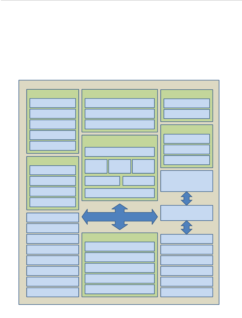
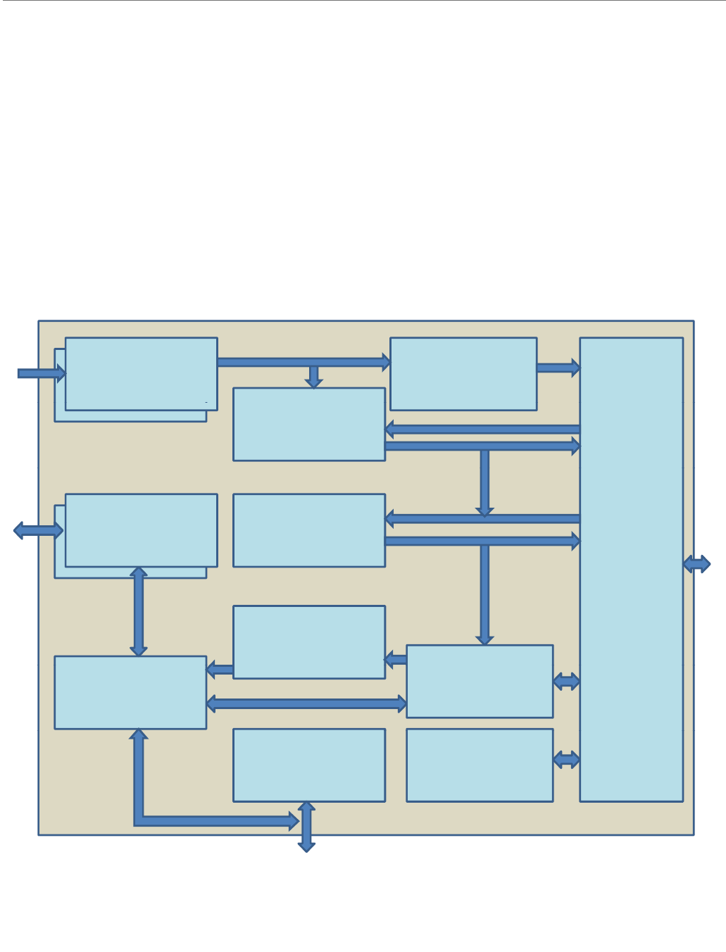
Block Diagram
The next figures show the block diagram of the Freescale i.MX515 CPU and the block diagram
of the ConnectCore for i.MX51 module.
CPU
Security
SAHARA v4
OpenGL
ES 2 0 + VG1 1
Mory
ROM 32KB
SAHARA
v4
Trust Zone
RTIC
SCC v2
OpenGL
ES
2
.
0
+
VG1
.
1
HW Video Codecs
HD720 TV-Out
ROM
32KB
RAM 96KB
rs
Ti
3
ARM
C
SRTC
Syste Control
Secure JTAG
Ti
mer x
3
PWM x 2
ARM
C
ore
600/800 Cortex-A8
32KB
I-Cache
32KB
D-Cache
256KB
L2-Cache
Power Mgmt
PLL x 3
Clock Reset
Neon
Vector Floag Point Unit
ETM
External Memory
Interface
Processin Unit
Fast IrDA
1-Wire
I2C x 2 HS MMC /SDIO x 4
Smart DMA
/AHBSwitch Fric
Dual-Display Controller
Image Signal Processor
Resizing & Blending
Inversion
&
Rotaon
GPIO
Keypad
USB OTG Host + PHY
SSI/I2S x 3
UART x 3
CSPI HS x 2 / LS x 1
Inversion
&
Rotaon
Dual-Camera Interface
USB Host x 3
Fuse Box
SPDIF Tx
10/100 Ethernet x
WatchDog x 2
ConnectCorefori.MX51
©2010DigiInternational,Inc. 13
Module
ConnectCore i.MX51
i
i.MX51 Module
180-p
i
n Connector
Memory
Timers
ARM
C
Security
System Control DDR2 Memory
Conguron
EMI
Interfces
IPU
ARM
C
ore
rt DMA
Interfes
NAND
Memory
C 3892
Eernet
HY
M
C
1
3892
l
Buck Switces
Bery Mgmt
b
Controller
WLAN
LDO Regu
l
or10-
b
it ADC
Touc I/F Boost Switc Ext
Power Supply
CPU I/FRTC / Osc
Accelerometer
180-pin Connector

ConnectCorefori.MX51
©2010DigiInternational,Inc. 14
Module Pinout
The module has two 180-pin connectors, J1 and J2. The next tables describe each pin, its
properties, and its use on the module and development board. The DC parameters for each
I/O type are defined in the “I/O DC Parameters” section of Appendix A - Specifications.
The “Use on module” column shows the connection of the signals in the module. The format
of this column is “component: pad_name,” where “component” is the chip where the signals
are connected, and “pad_name” is the name of the pad where the signals are connected as
they are defined in the component’s datasheet.
Pinout Legend
I Input
OOutput
I/O Input or output
PPower
# Low level active signal
J1 Pinout
Pin I/O Type Signal name Use on module Use on development board Comments
1 GPIO27 CSI1_D8/GPIO3_12 i.MX51: CSI1_D8 Not used
2 GPIO27 CSI1_D9/GPIO3_13 i.MX51: CSI1_D9 Camera 1 Reset
3 HSGPIO27 CSI1_D10 i.MX51: CSI1_D10 Camera 1 data
4 HSGPIO27 CSI1_D11 i.MX51: CSI1_D11 Camera 1 data
5 HSGPIO27 CSI1_D12 i.MX51: CSI1_D12 Camera 1 data
6 HSGPIO27 CSI1_D13 i.MX51: CSI1_D13 Camera 1 data
7 HSGPIO27 CSI1_D14 i.MX51: CSI1_D14 Camera 1 data
8 HSGPIO27 CSI1_D15 i.MX51: CSI1_D15 Camera 1 data
9 HSGPIO27 CSI1_D16 i.MX51: CSI1_D16 Camera 1 data
10 HSGPIO27 CSI1_D17 i.MX51: CSI1_D17 Camera 1 data
11 HSGPIO27 CSI1_D18 i.MX51: CSI1_D18 Camera 1 data
12 HSGPIO27 CSI1_D19 i.MX51: CSI1_D19 Camera 1 data
13 GPIO27 CSI1_VSYNC/GPIO3_14 i.MX51: CSI1_VSYNC Camera 1 vertical synchronization
14 GPIO27 CSI1_HSYNC/GPIO3_15 i.MX51: CSI1_HSYNC Camera 1 horizontal
synchronization
15 GPIO27 CSI1_PIXCLK i.MX51: CSI1_PIXCLK Camera 1 pixel clock
16 GPIO27 CSI1_MCLK i.MX51: CSI1_MCLK Camera 1 & 2 Master clock
17 - GND - -

ConnectCorefori.MX51
©2010DigiInternational,Inc. 15
18 - GND - -
19 WLAN WLAN_TDO WLAN: TDO Not Used
20 WLAN WLAN_TCK WLAN: TCK Not Used
21 WLAN WLAN_TDI WLAN: TDI Not Used
22 WLAN WLAN_TMS WLAN: TMS Not Used
23 WLAN WLAN_LED WLAN: LED_ON WLAN LED
24 WLAN RS_BT_PRIORITY WLAN: BT_PRIORITY Not Used
25 WLAN RS_WLAN_ACTIVE WLAN: WLAN_ACTIVE Not Used
26 WLAN RS_BT_ACTIVE WLAN: BT_ACTIVE Not Used
27 LVIO BOOT_MODE0 i.MX51: BOOT_MODE0 Boot Mode selection Boot configuration not
available in EA Kit
28 GPIO33 WLAN_DISABLE# WLAN Power Supply Switch WLAN Disable Jumper (J17) This signal switch ON/OFF
the supplu of WLAN
29 LVIO BOOT_MODE1 i.MX51: BOOT_MODE1 Boot Mode selection Boot configuration not
available in EA Kit
30 - - - -
31 - - - -
32 - - - -
33 - +2.775V - -
34 - - - -
35 - +2.775V - -
36 - +2.775V - -
37 PMIC_GPO MC13892_GPO1 MC13892: GPO1 Reserved
38 - +2.775V - -
39 PMIC_PWRON PMIC_PWRON1 MC13892: PWRON1 Connected to Power Button (S11) Suspend / Wake-up button
40 PMIC_STDBY PMIC_STDBY_REQ i.MX51: PMIC_STBY_REQ
MC13892: STANDBY
Reserved Output from i.MX51 to put
MC13892 in low power
mode
41 PMIC_INT PMIC_INT_REQ i.MX51: PMIC_INT_REQ Reserved This high-priority interrupt
input on i.MX51 is not used.
The output interrupt from
PMIC is connected to
standard interrupt GPIO_5 on
i.MX51.
42 PMIC_PWGTDRV PWRGTDRV1 MC13892: PWRGTDRV1 Not used
43 PMIC_LED CHRGLED MC13892: CHRGLED Battery Charging LED
Pin I/O Type Signal name Use on module Use on development board Comments

ConnectCorefori.MX51
©2010DigiInternational,Inc. 16
44 PMIC_PWGTDRV PWRGTDRV2 MC13892: PWRGTDRV2
+3.3V_REG: ENABLE
Not used Used on module to enable /
disable the +3.3V supply
45 PMIC_SE CHRGSE1# MC13892: CHRGSE1# Charger detection circuit This circuit is needed to boot
from charger
46 - VCC_COINCELL MC13892: LICELL Coincell voltage
47 - VLIO MC13892: BATT Battery supply
48 - VCHRG MC13892: CHRGRAW Charger supply
49 - VLIO MC13892: BATT Battery supply
50 - VCHRG MC13892:CHRGRAW Charger supply
51 - VLIO MC13892: BATT Battery supply
52 - VCHRG MC13892:CHRGRAW Charger supply
53 ETH ETH1_TX+ ETH_PHY: TXP Ethernet 1 Tx+
54 ETH ETH1_RX+ ETH_PHY: RXP Ethernet 1 Rx+
55 ETH ETH1_TX- ETH_PHY: TXN Ethernet 1 Tx-
56 ETH ETH1_RX- ETH_PHY: RXN Ethernet 1 Rx-
57 - GND - -
58 GPIO33 ETH1_LINK ETH_PHY: LED1 Ethernet 1 Link LED
59 GPIO27 DISPB2_SER_DIN/
GPIO3_5
i.MX51:
DISPB_2_SER_DIN
GPIO1 signal to LCD connectors
60 GPIO33 ETH1_ACTIVITY ETH_PHY: LED2 Ethernet 1 Activity LED
61 GPIO27 DISPB2_SER_RS/
GPIO3_8
i.MX51: DISPB2_SER_RS USB Host Reset In Early Availability Kit USB
host and Digital IO interface
cannot be used at the same
time.
62 GPIO27 DISPB2_SER_DIO/
GPIO3_6
i.MX51: DISPB2_SER_DIO User button 1 & Digital IO 7
63 GPIO27 DISP2_DATA0/
MII_RXD3/USBH3_CLK
i.MX51: DISP2_DATA0
ETH_PHY: RXD3
LCD2 Data Ethernet 1 and LCD2 cannot
be used at the same time.
64 GPIO27 DISPB2_SER_CLK_
GPIO3_7
i.MX51:
DISPB2_SER_CLK
Camera 2 Reset
65 HSGPIO27 DISP2_DATA2 i.MX51: DISP2_DATA2 LCD2 Data
66 GPIO27 DISP2_DATA1/
MII_RX_ER/USBH3_DIR
i.MX51: DISP2_DATA1
ETH_PHY: RXD4
LCD2 Data Ethernet 1 and LCD2 cannot
be used at the same time.
67 HSGPIO27 DISP2_DATA4 i.MX51: DISP2_DATA4 LCD2 Data
68 HSGPIO27 DISP2_DATA3 i.MX51: DISP2_DATA3 LCD2 Data
69 GPIO27 DISP2_DATA6/
MII_TXD1/USBH3_STP
i.MX51: DISP2_DATA6
ETH_PHY: TXD1
LCD2 Data Ethernet 1 and LCD2 cannot
be used at the same time.
Pin I/O Type Signal name Use on module Use on development board Comments

ConnectCorefori.MX51
©2010DigiInternational,Inc. 17
70 HSGPIO27 DISP2_DATA5 i.MX51: DISP2_DATA5 LCD2 Data Ethernet 1 and LCD2 cannot
be used at the same time.
71 GPIO27 DISP2_DATA8/
MII_TXD3/
USBH3_DATA0
i.MX51: DISP2_DATA8
ETH_PHY: TDX3
LCD2 Data Ethernet 1 and LCD2 cannot
be used at the same time.
72 GPIO27 DISP2_DATA7/
MII_TXD2/UBH3_NXT
i.MX51: DISP2_DATA7
ETH_PHY: TDX2
LCD2 Data Ethernet 1 and LCD2 cannot
be used at the same time.
73 GPIO27 DISP2_DATA10/
MII_COL/
USBH3_DATA2
i.MX51: DISP2_DATA10
ETH_PHY: COL
LCD2 Data Ethernet 1 and LCD2 cannot
be used at the same time.
74 GPIO27 DISP2_DATA9/
MII_TXEN/
USBH3_DATA1
i.MX51: DISP2_DATA9
ETH_PHY: TXEN
LCD2 Data Ethernet 1 and LCD2 cannot
be used at the same time.
75 GPIO27 DISP2_DAT12/
MII_RX_DV/
USBH3_DATA4
i.MX51: DISP2_DATA12
ETH_PHY: RXDV
LCD2 Data Ethernet 1 and LCD2 cannot
be used at the same time.
76 GPIO27 DISP2_DAT11/
MII_RX_CLK/
USBH3_DATA3
i.MX51: DISP2_DATA11
ETH_PHY: RXCLK
LCD2 Data Ethernet 1 and LCD2 cannot
be used at the same time.
77 GPIO27 DISP2_DATA14/
MII_RXD0/
USBH3_DATA6
i.MX51: DISP2_DATA14
ETH_PHY: RXD0
LCD2 Data Ethernet 1 and LCD2 cannot
be used at the same time.
78 GPIO27 DISP2_DAT13/
MII_TX_CLK/
USBH3_DATA5
i.MX51: DISP2_DATA13
ETH_PHY: TXCLK
LCD2 Data Ethernet 1 and LCD2 cannot
be used at the same time.
79 GPIO27 DI2_PIN2/MII_MDC i.MX51: DI2_PIN2
ETH_PHY: MDC
LCD2 Data Ethernet 1 and LCD2 cannot
be used at the same time.
80 GPIO27 DISP2_DAT15/
MII_TXD0/
USBH3_DATA7
i.MX51: DISP2_DATA15
ETH_PHY: TXD0
LCD2 Data Ethernet 1 and LCD2 cannot
be used at the same time.
81 GPIO27 DI2_PIN4/MII_CRS i.MX51: DI2_PIN4
ETH_PHY: CRS
LCD2 Data Ethernet 1 and LCD2 cannot
be used at the same time.
82 - GND - -
83 RGB IOR i.MX51: IOR Not used
84 GPIO27 DI2_DISP_CLK/
MII_RXD1
i.MX51: DI2_DISP_CLK
ETH_PHY: RXD1
LCD2 Data Ethernet 1 and LCD2 cannot
be used at the same time.
85 RGB IOR_BACK i.MX51: IOR_BACK Not used
86 GPIO27 DI2_PIN3/MII_MDIO i.MX51: DI2_PIN3
ETH_PHY: MDIO
LCD2 Data Ethernet 1 and LCD2 cannot
be used at the same time.
87 RGB IOB i.MX51: IOB Not useD
88 IOG IOG i.MX51: IOG Not used
89 RGB IOB_BACK i.MX51: IOB_BACK Not used
Pin I/O Type Signal name Use on module Use on development board Comments

ConnectCorefori.MX51
©2010DigiInternational,Inc. 18
90 RGB IOG_BACK i.MX51: IOG_BACK Not used
91 GPIO18 JTAG_TCK i.MX51: JTAG_TCK JTAG Connector
92 GPIO18 JTAG_TRST# i.MX51: JTAG_TRST# JTAG Connector
93 GPIO18 JTAG_TMS i.MX51: JTAG_TMS JTAG Connector
94 GPIO18 JTAG_MOD# i.MX51: JTAG_MOD# JTAG Mod Selection
95 GPIO18 JTAG_TDI i.MX51: JTAG_TDI JTAG Connector
96 GPIO18 JTAG_DE# i.MX51: JTAG_DE_B JTAG Connector
97 GPIO18 JTAG_TDO i.MX51: JTAG_TDO JTAG Connector
98 LVIO RESET_IN# i.MX51: RESET_IN_B
MC13892: RESETB
Not used Warm reset input to i.MX51.
99 LVIO POR# i.MX51: POR_B
MC13892: RESETBMCU
LCD 1 & 2 Reset, JTAG
Connector and Reset Button (S4)
Cold reset input to i.MX51.
Used to reset the module and
peripherals on the Dev. Kit.
100 - +1.8V -
101 - GND -
102 - GND -
103 ETH ETH2_TX+/ETH2_DA+ ETH_CTRL: TPO+ Ethernet 1 Tx+
104 ETH ETH2_RX+/ETH2_DB+ ETH_CTRL: TPI+ Ethernet 1 Rx+
105 ETH ETH2_TX+/ETH2_DA- ETH_CTRL: TPO- Ethernet 1 Tx-
106 ETH ETH2_RX+/ETH2_DB- ETH_CTRL: TPI- Ethernet 1 Rx-
107 - - - - -
108 - - - - -
109 - - - - -
110 - - - - -
111 GPIO33 ETH2_ACTIVITY# ETH_CTRL: GPIO1/LED2# Ethernet 2 Activity LED
112 GPIO33 ETH2_LINK# ETH_CTRL: GPIO0/LED1# Ethernet 2 Link LED
113 GPOIO18 EIM_CS0/GPIO2_25 i.MX51: EIM_CS0 Peripheral Application Chip Select
114 GPOIO18 EIM_CS1/GPIO2_26 i.MX51: EIM_CS1 Not used
115 GPOIO18 EIM_CS2/GPIO2_27 i.MX51: EIM_CS2 Not used
116 GPOIO18 EIM_CS3/GPIO2_28 i.MX51: EIM_CS3 Not used
117 GPOIO18 EIM_CS4/GPIO2_29 i.MX51: EIM_CS4 Not used
118 GPOIO18 EIM_CS5/LAN9221_CS#/
GPIO2_30
i.MX51: EIM_CS4
EHT_CTRL: CS#
Reserved
119 GPOIO18 EIM_DTACK/GPIO2_31 i.MX51: EIM_DTACK Not used
Pin I/O Type Signal name Use on module Use on development board Comments

ConnectCorefori.MX51
©2010DigiInternational,Inc. 19
120 GPOIO18 EIM_LBA/GPIO3_1 i.MX51: EIM_LBA Not used
121 GPOIO18 EIM_DA0/TRACE16 i.MX51: EIM_DA0
ETH_CTRL: A1
Peripheral Application Data /
Address
122 GPOIO18 EIM_DA1/TRACE17 i.MX51: EIM_DA1
ETH_CTRL: A2
Peripheral Application Data /
Address
123 GPOIO18 EIM_DA2/TRACE18 i.MX51: EIM_DA2
ETH_CTRL: A3
Peripheral Application Data /
Address
124 GPOIO18 EIM_DA3/TRACE19 i.MX51: EIM_DA3
ETH_CTRL: A4
Peripheral Application Data /
Address
125 - GND - -
126 GPOIO18 EIM_DA5/TRACE21 i.MX51: EIM_DA5
ETH_CTRL: A6
Peripheral Application Data /
Address
127 GPOIO18 EIM_DA4/TRACE20 i.MX51: EIM_DA4
ETH_CTRL: A5
Peripheral Application Data /
Address
128 GPOIO18 EIM_DA7/TRACE23 i.MX51: EIM_DA7
ETH_CTRL: FIFO_SEL
Peripheral Application Data /
Address
129 GPOIO18 EIM_DA6/TRACE22 i.MX51: EIM_DA6
ETH_CTRL: A7
Peripheral Application Data /
Address
130 - GND - -
131 GPOIO18 EIM_DA8/TRACE24 i.MX51: EIM_DA8 Peripheral Application Data /
Address
132 GPOIO18 EIM_DA9/TRACE25 i.MX51: EIM_DA9 Peripheral Application Data /
Address
133 GPOIO18 EIM_DA10/TRACE26 i.MX51: EIM_DA10 Not used
134 GPOIO18 EIM_DA11/TRACE27 i.MX51: EIM_DA11 Not used
135 - GND - -
136 GPOIO18 EIM_DA13/TRACE29 i.MX51: EIM_DA13 Not used
137 GPOIO18 EIM_DA12/TRACE28 i.MX51: EIM_DA12 Not used
138 GPOIO18 EIM_DA15/TRACE31 i.MX51: EIM_DA15 Not used
139 GPOIO18 EIM_DA14/TRACE30 i.MX51: EIM_DA14 Not used
140 - GND - -
141 GPOIO18 EIM_D16/TRACE0 i.MX51: EIM_D16
ETH_CTRL: D0
Peripheral Application Data
142 GPOIO18 EIM_D17/TRACE1 i.MX51: EIM_D17
ETH_CTRL: D1
Peripheral Application Data
143 GPOIO18 EIM_D18/TRACE2 i.MX51: EIM_D18
ETH_CTRL: D2
Peripheral Application Data
Pin I/O Type Signal name Use on module Use on development board Comments

ConnectCorefori.MX51
©2010DigiInternational,Inc. 20
144 GPOIO18 EIM_D19/TRACE3 i.MX51: EIM_D19
ETH_CTRL: D3
Peripheral Application Data
145 - +3.15V - -
146 GPOIO18 EIM_D21/TRACE5 i.MX51: EIM_D21
ETH_CTRL: D5
Peripheral Application Data
147 GPOIO18 EIM_D20/TRACE4 i.MX51: EIM_D20
ETH_CTRL: D4
Peripheral Application Data
148 GPOIO18 EIM_D23//TRACE7 i.MX51: EIM_D23
ETH_CTRL: D7
Peripheral Application Data
149 GPOIO18 EIM_D22/TRACE6 i.MX51: EIM_D22
ETH_CTRL: D8
Peripheral Application Data
150 - GND - -
151 GPOIO18 EIM_D24/TRACE8 i.MX51: EIM_D24
ETH_CTRL: D8
Peripheral Application Data
152 GPOIO18 EIM_D25/TRACE9 i.MX51: EIM_D25
ETH_CTRL: D9
Peripheral Application Data
153 GPOIO18 EIM_D26/TRACE10 i.MX51: EIM_D26
ETH_CTRL: D10
Peripheral Application Data
154 GPOIO18 EIM_D27/TRACE11 i.MX51: EIM_D27
ETH_CTRL: D11
Peripheral Application Data
155 - GND - -
156 GPOIO18 EIM_D29/TRACE13 i.MX51: EIM_D29
ETH_CTRL: D13
Peripheral Application Data
157 GPOIO18 EIM_D28/TRACE12 i.MX51: EIM_D28
ETH_CTRL: D12
Peripheral Application Data
158 GPOIO18 EIM_D31/TRACE15 i.MX51: EIM_D31
ETH_CTRL: D15
Peripheral Application Data
159 GPOIO18 EIM_D30/TRACE14 i.MX51: EIM_D30
ETH_CTRL: D14
Peripheral Application Data
160 GPOIO18 EIM_A17/GPIO2_11 i.MX51: EIM_A17 Not used
161 GPOIO18 EIM_A16/GPIO2_10 i.MX51: EIM_A16 Not used
162 GPOIO18 EIM_A19/GPIO2_13 i.MX51: EIM_A19 Not used
163 GPOIO18 EIM_A18/GPIO2_12 i.MX51: EIM_A18 Not used
164 GPOIO18 EIM_A21/GPIO2_15 i.MX51: EIM_A21 Boot Configuration Switch
165 GPOIO18 EIM_A20/GPIO2_14 i.MX51: EIM_A20 Boot Configuration Switch
166 GPOIO18 EIM_A23/GPIO2_17 i.MX51: EIM_A23 Not used
167 GPOIO18 EIM_A22/GPIO2_16 i.MX51: EIM_A22 Not used
Pin I/O Type Signal name Use on module Use on development board Comments

ConnectCorefori.MX51
©2010DigiInternational,Inc. 21
J2 Pinout
168 GPOIO18 EIM_A25/GPIO2_19 i.MX51: EIM_A25 Not used
169 GPOIO18 EIM_A24/GPIO2_18 i.MX51: EIM_A24 Not used
170 GPOIO18 EIM_A27/GPIO2_21 i.MX51: EIM_A27 XBEE_SLEEP_RQ
171 GPOIO18 EIM_A26/GPIO2_20 i.MX51: EIM_A26 Not used
172 GPOIO18 EIM_OE#/GPIO2_24 i.MX51: EIM_OE
ETH_CTRL: RD#
Peripheral Application Output
Enable
173 GPOIO18 EIM_EB0 i.MX51: EIM_EB0 Not used
174 GPOIO18 EIM_RW# i.MX51: EIM_RW
ETH_CTRL: WR#
Peripheral Application Read /
Write
175 GPOIO18 EIM_EB1 i.MX51: EIM_EB1 Not used
176 GPOIO18 EIM_CRE/GPIO3_2 i.MX51: EIM_CRE Peripheral Application Interrupt
input
177 GPOIO18 EIM_EB2/GPIO2_22/
TRCTL
i.MX51: EIM_EB2 Peripheral Application Byte
Enable 2
178 GPOIO18 EIM_WAIT i.MX51: EIM_WAIT Not used
179 GPOIO18 EIM_EB3/GPIO2_23/
TRCLK
i.MX51: EIM_EB3 Peripheral Application Byte
Enable 3
180 GPOIO18 EIM_BCLK i.MX51: EIM_BCLK Peripheral Application Clock Burst By default not connected on
Development Board.
Pin Type Signal name Use on module Use on development board Comments
1HSGPIO27 DISP1_DAT0 i.MX51: DISP1_DAT0 HDMI, VGA and LCD1 Data
2HSGPIO27 DISP1_DAT1 i.MX51: DISP1_DAT1 HDMI, VGA and LCD1 Data
3HSGPIO27 DISP1_DAT2 i.MX51: DISP1_DAT2 HDMI, VGA and LCD1 Data
4HSGPIO27 DISP1_DAT3 i.MX51: DISP1_DAT3 HDMI, VGA and LCD1 Data
5HSGPIO27 DISP1_DAT4 i.MX51: DISP1_DAT4 HDMI, VGA and LCD1 Data
6HSGPIO27 DISP1_DAT5 i.MX51: DISP1_DAT5 HDMI, VGA and LCD1 Data
7GPIO27 DISP1_DAT6 i.MX51: DISP1_DAT6 HDMI, VGA and LCD1 Data, Boot
Configuration
8GPIO27 DISP1_DAT7 i.MX51: DISP1_DAT7 HDMI, VGA and LCD1 Data, Boot
Configuration
Pin I/O Type Signal name Use on module Use on development board Comments

ConnectCorefori.MX51
©2010DigiInternational,Inc. 22
9GPIO27 DISP1_DAT8 i.MX51: DISP1_DAT8 HDMI, VGA and LCD1 Data, Boot
Configuration
On Development Kit DISP1
and DISP2 are configured at
18-bit, and connected to 24-
bit LCDs.
On Development Kit some
DISP1 signals are used to
configure the boot process.
On Early Availability Kit
DISP1 and DISP2 are
configured at 24-bit, and
connected to 24-bit LCDs.
10 GPIO27 DISP1_DAT9 i.MX51: DISP1_DAT9 HDMI, VGA and LCD1 Data, Boot
Configuration
11 GPIO27 DISP1_DAT10 i.MX51: DISP1_DAT10 HDMI, VGA and LCD1 Data, Boot
Configuration
12 GPIO27 DISP1_DAT11 i.MX51: DISP1_DAT11 HDMI, VGA and LCD1 Data, Boot
Configuration
13 GPIO27 DISP1_DAT12 i.MX51: DISP1_DAT12 HDMI, VGA and LCD1 Data, Boot
Configuration
14 GPIO27 DISP1_DAT13 i.MX51: DISP1_DAT13 HDMI, VGA and LCD1 Data, Boot
Configuration
15 GPIO27 DISP1_DAT14 i.MX51: DISP1_DAT14 HDMI, VGA and LCD1 Data, Boot
Configuration
16 GPIO27 DISP1_DAT15 i.MX51: DISP1_DAT15 HDMI, VGA and LCD1 Data, Boot
Configuration
17 GPIO27 DISP1_DAT16 i.MX51: DISP1_DAT16 HDMI, VGA and LCD1 Data, Boot
Configuration
18 GPIO27 DISP1_DAT17 i.MX51: DISP1_DAT17 HDMI, VGA and LCD1 Data, Boot
Configuration
19 GPIO27 DISP1_DAT18 i.MX51: DISP1_DAT18 Not used
20 GPIO27 DISP1_DAT19 i.MX51: DISP1_DAT19 Not used
21 GPIO27 DISP1_DAT20 i.MX51: DISP1_DAT20 Boot Configuration
22 GPIO27 DISP1_DAT21 i.MX51: DISP1_DAT21 Boot Configuration
23 GPIO27 DISP1_DAT22 i.MX51: DISP1_DAT22 LCD2 Data
24 GPIO27 DISP1_DAT23 i.MX51: DISP1_DAT23 LCD2 Data
25 GPIO27 DI1_PIN2 i.MX51: DI1_PIN2 HDMI, VGA and LCD1 HSYNC
26 -GND - -
27 GPIO27 DI1_PIN11/GPIO3_0 i.MX51: DI1_PIN11 LCD1 PWREN#
28 GPIO27 DI1_DISP_CLK i.MX51: DI1_DISP_CLK HDMI, VGA and LCD1 Clock
29 GPIO27 DI1_PIN13/GPIO3_2 i.MX51: DI1_PIN13 LCD1 and LCD2 GPIO2
30 GPIO27 DI1_PIN3 i.MX51: DI1_PIN3 HDMI, VGA and LCD1 VSYNC
31 GPIO27 DI1_PIN15 i.MX51: DI1_PIN15 HDMI, VGA and LCD1 DRDY
32 GPIO27 DI1_PIN12/GPIO3_1 i.MX51: DI1_PIN12 LCD2 PWREN#
33 GPIO27 DI_GP2 i.MX51: DI_GP2 Not used
34 GPIO27 DI_GP1 i.MX51: DI_GP1 Not used
Pin Type Signal name Use on module Use on development board Comments

ConnectCorefori.MX51
©2010DigiInternational,Inc. 23
35 GPIO27 DI_GP4/MII_RXD2 i.MX51: DI_GP4
LAN8710: RXD2
LCD2 DRDY
36 GPIO27 DI_GP3/MII_TX_ER i.MX51: DI_GP3
LAN8710: INT#/TXER/
TXD4
Not used
37 GPIO27 DI1_D1_CS/GPIO3_4 i.MX51: DI_D1_CS LCD1 and LCD2 Touch selection
input
38 GPIO27 DI1_D0_CS/GPIO3_3 i.MX51: DI_D0_CS LCD1 and LCD2 Touch selection
input
39 ADIN TOUCH_X1 MC13892: TSX1 LCD1 and LCD2 Touch X1 Analog input from Touch
Screen
40 ADIN ADIN5 MC13892: ADIN5 Reserved
41 ADIN TOUCH_X2 MC13892: TSX2 LCD1 and LCD2 Touch X2 Analog input from Touch
Screen
42 ADIN ADIN6 MC13892: ADIN6 Not used Analog input
43 ADIN TOUCH_Y1 MC13892: TSY1 LCD1 and LCD2 Touch Y1 Analog input from Touch
Screen
44 ADIN ADIN7 MC13892: ADIN7 Not used Analog input
45 ADIN TOUCH_Y2 MC13892: TSY2 LCD1 and LCD2 Touch Y2 Analog input from Touch
Screen
46 -ADC_GND - -
47 -GND - -
48 PMIC_STDBY ADTRIG MC13892: ADTRIG Not used
49 -SWBST MC13892: SWBST
MC13892: VINUSB
-Used in the module to power
USB PHY
50 -LEDKP MC13892: LEDKP Reserved
51 PMIC_LED LEDR MC13892: LEDR Not used
52 -LEDAD MC13892: LEDAD Reserved
53 PMIC_LED LEDG MC13892: LEDG Not used
54 -LEDMD MC13892: LEDMD Reserved
55 PMIC_LED LEDB MC13892: LEDB Not used
56 -VSWLED - -
57 GPIO27 CSI2_D12/GPIO4_9 i.MX51: CSI2_D12 Camera 2 Data
58 GPIO27 CSI2_D13/GPIO4_10 i.MX51: CSI2_D13 Camera 2 Data
59 HSGPIO27 CSI2_D14 i.MX51: CSI2_D14 Camera 2 Data
60 HSGPIO27 CSI2_D15 i.MX51: CSI2_D15 Camera 2 Data
61 HSGPIO27 CSI2_D16 i.MX51: CSI2_D16 Camera 2 Data
Pin Type Signal name Use on module Use on development board Comments

ConnectCorefori.MX51
©2010DigiInternational,Inc. 24
62 HSGPIO27 CSI2_D17 i.MX51: CSI2_D17 Camera 2 Data
63 GPIO27 CSI2_D18/GPIO4_11 i.MX51: CSI2_D18 Camera 2 Data
64 GPIO27 CS12_D19/GPIO4_12 i.MX51: CSI2_D19 Camera 2 Data
65 GPIO27 CSI1_VSYNC/GPIO4_13 i.MX51: CSI2_VSYNC Camera 2 VSYNC
66 GPIO27 CSI2_HSYNC/GPIO4_14 i.MX51: CSI2_HSYNC Camera 2 HSYNC
67 GPIO27 CSI2_PIXCLK_GPIO4_15 i.MX51: CSI2_PIXCLK Camera 2 PIXCLK
68 -GND -
69 -GND -
70 DIG_USB USB_OTG_ID i.MX51: ID USB OTG ID
71 AN_USB USB_OTG_DP i.MX51: DP USB OTG DP
72 -USB_OTG_VBUS i.MX51: VBUS USB OTG VBUS
73 AN_USB USB_OTG_DN i.MX51: DN USB OTG DN
74 GPIO27 GPIO1_8/USB_PWR i.MX51: GPIO_8 Not used
75 -GND - -
76 GPIO27 GPIO1_2/PWM1/
I2C2_SCL
i.MX51: GPIO1_2
MMA7455LR1:SCL
I2C Bus Clock
77 GPIO27 GPIO1_7/
MMA7455LR_INT1
i.MX51: GPIO1_7
MMA7455LR1:INT1
Reserved Accelerometer Interrupt
78 GPIO27 GPIO1_3/PWM2/
I2C2_SDA
i.MX51: GPIO1_3
MMA7455LR1:SD
I2C Bus Clock
79 GPIO27 GPIO1_6/
MMA7455LR_INT2
i.MX51: GPIO1_6
MMA7455LR1:INT2
Reserved Accelerometer Interrupt
80 PMIC_INT CLK32K_PER MC13892: CLK32K Not used
81 -GND - -
82 -GND - -
83 -CKIH1 i.MX51: CKIH1 Not used
84 -CKIH2 i.MX51: CKIH2 Not used
85 UHVIO33 SD2_DATA0/
SD1_DATA1/SPI_MOSI
i.MX51: GPIO1_6
WLAN: SDIO_DATA0
Reserved SD bus 2 connected to
WLAN.
In modeules without WLAN
this SD bus can be used in the
development boards.
86 UHVIO33 SD2_CLK/I2C1_SDA/
SPI_SCLK
i.MX51: SD2_CLK
WLAN: SDIO_CLK
Reserved
87 UHVIO33 SD2_DATA1/
SD1_DATA5
i.MX51: SD2_DATA1
WLAN: SDIO_DATA1
Reserved
88 UHVIO33 SD2_CMD/I2C1_SCL/
SPI_MOSI
i.MX51: SD2_CMD
WLAN: SDIO_CMD
Reserved
Pin Type Signal name Use on module Use on development board Comments

ConnectCorefori.MX51
©2010DigiInternational,Inc. 25
89 UHVI0O3 SD2_DATA2/
SDI_DATA6
i.MX51: SD2_DATA2
WLAN: SDIO_DATA2
Reserved
90 GPIO27 KEY_COL0 i.MX51: KEY_COL0 XBee Reset#
91 UHVIO33 SD2_DATA3/
SD1_DATA7/SPI_SS2
i.MX51: SD2_DATA3
WLAN: SDIO_DATA3
Reserved
92 GPIO27 KEY_COL1 i.MX51: KEY_COL1 Not used
93 GPIO27 KEY_ROW0 i.MX51: ROW0 Not used
94 GPIO27 KEY_COL2 i.MX51: KEY_COL2 Not used
95 GPIO27 KEY_ROW1 i.MX51: ROW1 Not used
96 GPIO27 KEY_COL3 i.MX51: KEY_COL3 Not used
97 GPIO27 KEY_ROW2 i.MX51: ROW2 Not used
98 GPIO27 KEY_COL5/
UART3_CTS#/I2C1_SDA
i.MX51: KEY_COL5 XBee RTS#
99 GPIO27 KEY_ROW3 i.MX51: KEY_ROW3 Not used
100 GPIO27 GPIO1_0/SD1_CD#/
SPI_SS2
i.MX51: GPIO1_0 HDMI Interrupt
101 GPIO27 KEY_COL4/
UART3_RTS#/I2C2_SCL
i.MX51: KEY_COL4 XBee/UART3 RTS selection
102 GPIO27 GPIO1_1/SD1_WP#/
SPI_MISO
i.MX51: GPIO1_1 User Button 2
103 GPIO27 OWIRE_LINE/GPIO1_24 i.MX51: OWIRE_LINE One-Wire, HDMI SPDIF
104 UHVIO31 SD1_DATA0/
AUD5_TXD/SPI_MOSI
i.MX51: SD1_DATA0 MicroSD TM Data
105 UHVIO31 SD1_CMD/AUD5_RXFS/
SPI_MOSI
i.MX51: SD1_CMD MicroSD TM Command
106 UHVIO31 SD1_DATA1/
AUD5_RXD
i.MX51: SD1_DATA1 MicroSD TM Data
107 UHVIO31 SD1_CLK/AUD5_RXC/
SPI_SCLK
i.MX51: SD1_CLK MicroSD TM Clock
108 UHVIO31 SD1_DATA2/AUD5_TXC i.MX51: SD1_DATA2 MicroSD TM Data
109 GPIO27 WDOG1# i.MX51: GPIO1_4 Reserved HDMI Interrupt and PMIC
Watchdog input cannot be
used at the same time.
110 UHVIO31 SD1_DATA3/
AUD5_TXFS/SPI_SS1
i.MX51: SD1_DATA3 MicroSD TM Data
111 GPIO27 CSPI1_MOSI/I2C1_SDA/
GPIO4_22
i.MX51: CSPI1_MOSI
MC13892: MOSI
SPI_MOSI
112 GPIO27 CSPI1_SS0_PMIC/
AUD4_TXC/GPIO4_24
i.MX51: CSPI1_SS0
MC13892: CS
Reserved
Pin Type Signal name Use on module Use on development board Comments

ConnectCorefori.MX51
©2010DigiInternational,Inc. 26
113 GPIO27 CSPI1_MISO/
AUD4_RXD/GPIO4_23
i.MX51: CSPI1_MISO
MC13892: CS
SPI_MISO
114 GPIO27 CSPI1_SS1/AUD4_TXD/
GPIO4_25
i.MX51: CSPI1_SS1 SPI_SS1
115 GPIO27 CSPI1_SCLK/I2C1_SDA/
GPIO4_27
i.MX51: CSPI1_SCLK
MC13892: CLK
SPI_SCLK
116 GPIO27 CSPI1_RDY/
AUD4_TXFS/GPIO4_26
i.MX51: CSPI1_RDY LCD1 and LCD2 SPI Chip Select
117 GPIO27 UART1_RXD/GPIO4_28 i.MX51: UART1_RXD UART1 MEI
118 GPIO27 UART1_RTS#/GPIO4_30 i.MX51: UART1_RTS UART1 MEI
119 GPIO27 UART1_TXD/PWM2/
GPIO4_29
i.MX51: UART1_TXD UART1 MEI
120 GPIO27 UART1_CTS#/GPIO4_31 i.MX51: UART1_CTS UART1 MEI
121 GPIO27 UART2_RXD/GPIO1_20 i.MX51: UART2_RXD UART2 Console
122 GPIO27 UART3_RXD/
UART1_DTR#/GPIO1_22
i.MX51: UART3_RXD UART3/XBee
123 GPIO27 UART2_TXD/GPIO1_21 i.MX51: UART2_TXD UART2 Console
124 GPIO27 UART3_TXD/
UART1_DSR#/GPIO1_23
i.MX51: UART3_TXD UART3/XBee
125 GPIO27 USBH1_DATA2/
UART2_TXD_GPIO1_13
i.MX51: USBH1_DATA2 USB Host
126 -GND - -
127 GPIO27 USBH1_DATA4/
CSPI_SS0/GPIO1_15
i.MX51: USBH1_DATA4 USB Host
128 GPIO27 USBH1_DATA0/
UART2_CTS#/GPIO1_11
i.MX51: USBH1_DATA0 USB Host (default) and UART2
Console
129 GPIO27 USBH1_DATA6/
CSPI_SS2/GPIO1_17
i.MX51: USBH1_DATA6 USB Host
130 GPIO27 USBH1_DATA1/
UART2_RXD/GPIO1_12
i.MX51: USBH1_DATA1 USB Host
131 GPIO27 USBH1_DIR/SPI_MOSI/
GPIO1_26/I2C2_SDA
i.MX51: USBH1_DIR USB Host
132 GPIO27 USBH1_DATA3/
UART2_RTS#/GPIO1_14
i.MX51: USBH1_DATA3 USB Host (default) and UART2
Console
133 GPIO27 USBH1_STP/SPI_RDY/
GPIO1_27
i.MX51: USBH1_STP USB Host
134 GPIO27 USBH1_DATA5/
UART2_RTS#/GPIO1_14
i.MX51: USBH1_DATA5 USB Host
135 GPIO27 USBH1_NXT/SPI_MISO/
GPIO1_28
i.MX51: USBH1_NXT USB Host
Pin Type Signal name Use on module Use on development board Comments

ConnectCorefori.MX51
©2010DigiInternational,Inc. 27
136 GPIO27 USBH1_DATA7/
SPI_SS3/SPI2_SS3/
GPIO1-18
i.MX51: USBH1_DATA7 USB Host
137 GPIO27 AUD3_BB_TXD/
GPIO4_18
i.MX51: AUD3_BB_TXD Audio CODEC and HDMI Audio
138 GPIO27 USBH1_CLK/SPI_SCLK/
GPIO1_25/I2C2_SCL/
i.MX51: USBH1_CLK USB Host
139 GPIO27 AUD3_BB_RXD/
UART3_RXD/GPIO4_19
i.MX51: AUD_BB_RXD Audio CODEC
140 -HS_I2C_SCL/GPIO4_16 i.MX51: I2C_SCL Not used The HS_I2C interface is not
working in i.MX51.
141 GPIO27 AUD3_BB_CK/GPIO4_20 i.MX51: AUD_BB_CK Audio CODEC and HDMI Audio
142 -HS_I2C_SDA/GPIO4_17 i.MX51: I2C_SDA Not used The HS_I2C interface is not
working in i.MX51.
143 -+3.3V - -
144 GPIO27 AUD3_BB_FS/
UART3_TXD/GPIO4_21
i.MX51: AUD_BB_FS Audio CODEC and HDMI Audio
145 UHVIO31 NANDF_D0/PATA_D0/
SD4_DATA7/GPIO4_8
i.MX51: NANDF_D0
NAND_FLASH: I/O0
Reserved
146 -+3.3V - -
147 UHVIO31 NANDF_D2/PATA_D2/
SD4_DATA5/GPIO4_6
i.MX51: NANDF_D2
NAND_FLASH: I/O2
Reserved
148 UHVIO31 NANDF_D1/PATA_D1/
SD4_DATA6/GPIO4_7
i.MX51: NANDF_D1
NAND_FLASH: I/O1
Reserved
149 UHVIO31 NANDF_D4/PATA_D4/
SD4_CD/GPIO4_4
i.MX51: NANDF_D4
NAND_FLASH: I/O4
Reserved
150 UHVIO31 NANDF_D3/PATA_D3/
SD4_DATA4/GPIO4_5
i.MX51: NANDF_D3
NAND_FLASH: I/O3
Reserved
151 UHVIO31 NANDF_D6/PATA_D6/
SD4_LCTL/GPIO4_2
i.MX51: NANDF_D6
NAND_FLASH: I/O6
Reserved
152 UHVIO31 NANDF_D5/PATA_D5/
SD4_WP/GPIO4_3
i.MX51: NANDF_D5
NAND_FLASH: I/O5
Reserved
153 UHVIO31 NANDF_D8/PATA_D8/
GPIO4_0/SD3_DATA0
i.MX51: NANDF_D8 SD/MMC Data
154 UHVIO31 NANDF_D7/PATA_D7/
GPIO4_1
i.MX51: NANDF_D7
NAND_FLASH: I/O7
Reserved
155 UHVIO31 NANDF_D10/
PATA_D10/GPIO3_30/
SD3_D2
i.MX51: NANDF_D10 SD/MMC Data
Pin Type Signal name Use on module Use on development board Comments

ConnectCorefori.MX51
©2010DigiInternational,Inc. 28
156 UHVIO31 NANDF_D9/PATA_D9/
GPIO3_31/SD3_D1
i.MX51: NANDF_D9 SD/MMC Data
157 UHVIO31 NANDF_D12/
PATA_D12/GPIO3_28/
SD3_D4
i.MX51: NANDF_D12 SD/MMC Data
158 UHVIO31 NANDF_D11/
PATA_D11/GPIO3_29/
SD3_D3
i.MX51: NANDF_D11 SD/MMC Data
159 UHVIO31 NANDF_D14/
PATA_D14/GPIO3_26/
SD3_D6
i.MX51: NANDF_D14 SD/MMC Data
160 UHVIO31 NANDF_D13/
PATA_D13/GPIO3_27/
SD3_D5
i.MX51: NANDF_D13 SD/MMC Data
161 UHVIO31 NANDF_CS0#/GPIO3_16 i.MX51: NANDF_CS0
NAND_FLASH: CE#
Reserved
162 UHVIO31 NANDF_D15/
PATA_D15/GPIO3_25/
SD3_D7
i.MX51: NANDF_D15 SD/MMC Data
163 UHVIO31 NANDF_CS2#/
PATA_CS0#/GPIO3_18
i.MX51: NANDF_CS2
NAND_FLASH: NC
Digital I/O Connector
164 UHVIO31 NANDF_CS1#/GPIO3_17 i.MX51: NANDF_CS1
NAND_FLASH: NC
SD/MMC Write Protect
165 UHVIO31 NANDF_CS4#/
PATA_DA0/GPIO3_20
i.MX51: NANDF_CS4 Digital I/O Connector
166 UHVIO31 NANDF_CS3#/
PATA_CS1#/GPIO3_19
i.MX51: NANDF_CS3
NAND_FLASH: NC
HDMI audio clock enable
167 UHVIO31 NANDF_CS6#/
PATA_DA2/GPIO3_22
i.MX51: NANDF_CS6 Digital I/O Connector
168 UHVIO31 NANDF_CS5#/
PATA_DA1/GPIO3_21
i.MX51: NANDF_CS5 Digital I/O Connector
169 UHVIO31 NANDF_RDY_INT/
GPIO3_24
i.MX51:
NANDF_RDY_INT
SD/MMC Command
170 UHVIO31 NANDF_CS7#/GPIO3_23 i.MX51: NANDF_CS7 SD/MMC Clock SD clock and Digital IO
cannot be used at the same
time.
171 UHVIO31 NANDF_WE#/
PATA_DIOW/GPIO3_3
i.MX51: NANDF_WE_B
NAND_FLASH: WE#
Reserved
172 UHVIO31 GPIO_NAND/
PATA_INTRQ/GPIO3_12
i.MX51: GPIO_NAND SD/MMC Card Detect
173 UHVIO31 NANDF_ALE/
PATA_BUFFER_EN/
GPIO3_5
i.MX51: NANDF_ALE
NAND_FLASH: ALE
Reserved
Pin Type Signal name Use on module Use on development board Comments

ConnectCorefori.MX51
©2010DigiInternational,Inc. 29
174 UHVIO31 NANDF_RE#/
PATA_DIOR/GPIO3_4
i.MX51: NANDF_RE_B
NAND_FLASH: RE#
Reserved
175 UHVIO31 NANDF_WP#/
PATA_DMACK/GPIO3_7
i.MX51: NANDF_WP_B
NAND_FLASH: WP#
Reserved
176 UHVIO31 NANDF_CLE/
PATA_RESET/GPIO3_6
i.MX51: NANDF_CLE
NAND_FLASH: CLE
Reserved
177 UHVIO31 NANDF_RB1/
PATA_IORDY/GPIO3_9
i.MX51: NANDF_RB1
NAND_FLASH: NC
User LED2 and Digital I/O
Connector
178 UHVIO31 NANDF_RB0/
PATA_DMARQ/GPIO3_8
i.MX51: NANDF_RB0
NAND_FLASH: R/B#
Reserved
179 UHVIO31 NANDF_RB3/GPIO3_11 i.MX51: NANDF_RB3
NAND_FLASH: NC
Digital I/O Connector
180 UHVIO31 NANDF_RB2/GPIO3_10 i.MX51: NANDF_RB2
NAND_FLASH: NC
User LED1 and Digital I/O
Connector
Pin Type Signal name Use on module Use on development board Comments
ConnectCorefori.MX51
©2010DigiInternational,Inc. 30
Power
Module Power Supplies
The following figure shows the power supply scheme of the ConnectCore for i.MX51 module.
Supply Inputs
The ConnectCore for i.MX51module has the following supply inputs:
Battery input (VLIO)
Charger input (VCHRG)
Coin Cell input (VCC_COINCELL)
Battery input (VLIO)
The VLIO supply is used to generate all the voltage supplies needed in the module by the
ConnectCore for i.MX51 CPU and by the peripherals. The minimum voltage of VLIO to allow
the module to turn on is +3.4V. The maximum voltage of VLIO is +4.8V.
Charger input (VCHRG)
The battery charger supply is used to charge rechargeable batteries, as well as to power up
the module when there is no battery or the battery is discharged. The minimum voltage of
the battery charger is +3.4V. The maximum voltage of the battery charger is +20V.

ConnectCorefori.MX51
©2010DigiInternational,Inc. 31
Coin Cell input (VCC_COINCELL)
A connection for a coin cell or supercap is provided at VCC_COINCELL. From the coin cell the
RTC remains supplied in case of absense of the main battery. A low current 60uA charger is
included which will change the coin cell to a programmable voltage of +2.5V to +3.3V. In case
the module is turned off, it is ensured that the coin cell charge is maintained as long as a
valid main battery is in place. The behavior of the coin cell charger is programmable.
The following table shows the current draw from the coin cell when there is no main battery
attached:
The maximum voltage of the coin cell supply is +2V. The maximum voltage of the coin cell
supply is +3.6V.
Supply Outputs
The ConnectCore for 1.MX51 module provides the following supply outputs:
+3.3V
+2.775V
SWBT (+5V)
+1.8V
+3.15V
+3.3V
The ConnectCore for i.MX51 module has a DC/DC converter to generate a +3.3V supply. This
supply is used in the module to power the WLAN interface, the Ethernet 1PHY and the second
Ethernet Controller.
This power regulator can be enabled/disabled by the software to save power when the
module is in the low power modes. The maximum current provider by this regulator is 1A.
+2.775V
This supply is used in the module to power the ConnectCore for i.MX51 peripherals, the
accelerometer and the ConnectCore for i.MX51 image processing unit. The maximum current
provided by this supply is 100mA.
SWBT (+5V)
The voltage level of the SWBT supply is +5V. The maximum current provided by this supply is
300mA.
+1.8V
This supply is used in the module to power the external memory interface (EMI) and the JTAG
interface. The maximum current provider by this supply is 800mA.
Mode Description Typ Max Unit
RTC All blocks disabled, no main battery
attached, coin cell is attached.
37uA
ConnectCorefori.MX51
©2010DigiInternational,Inc. 32
+3.15V
This supply is used in the module to power the NAND Flash interface and the SD-card 1
interface. The maximum current provided by this supply is 350mA.
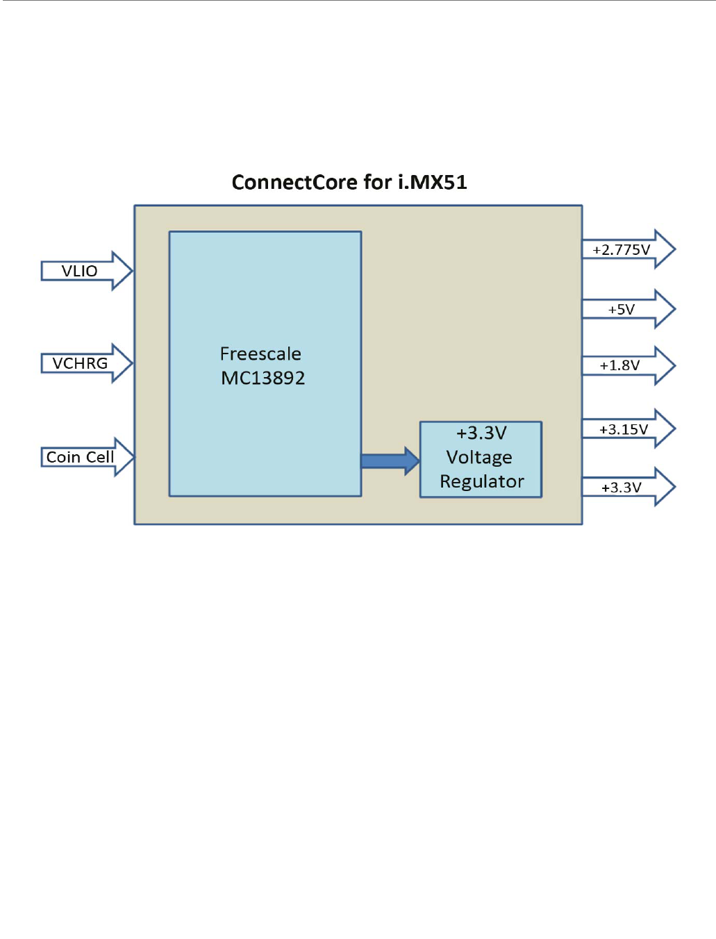
MC13892 Power Management
The ConnectCore for i.MX51 module is designed with Freescale MC13892 Power Management
chip. This chip provides reference and supply voltages for the i.MX51 as well as for the
peripheral devices. The MC13892 has four buck switchers, one +5V boost switcher and twelve
low dropout regulators as well as other user interfaces. The following figure shows the block
diagram of the MC13892.
MC13892
Battery
Management
4Buck
Switchers
12LDO
Regulators
Backlight
Drivers
10BitADC Bias &
References
+5VBoost
Switcher
LED
Drivers
Touch Screen
Interface
Power
ControlLogic
32.768KHz Control
Interface
Processor Logic Interfacing

ConnectCorefori.MX51
©2010DigiInternational,Inc. 33
Memory
DDR2 SDRAM Memory
The ConnectCore for i.MX51 module provides up to 512 MBytes of DDR2-400 SDRAM memory.
The module can support up to four 16-bit, 128Mbit, DDR2-400 chips, configured as two banks
of 32-bits of 128Mbits DDR2-400 memory.
NAND Flash Memory
The ConnectCore for i.MX51 module provides 512Mbytes of NAND-Flash memory. On the
module a 512MByte, 2Kbyte page, NAND-Flash chip is used.
Options for other densities NAND Flash devices are available depending on the module
variant.
Chip selects
Chip Select Memory Map
The ConnectCore for i.MX51 has eight chip select signals, two for dynamic memory and six for
static memory. The table below shows the memory map of these chip select signals.
Name Pin Address range Sixe [Mb] Usage Comments
DRAM_CS0# Y4 0x9000_000-
0x9FFF_FFFF
256M DDR2 bank 0 First bank on module
DRAM_CS1# Y3 0xA000_0000-
0xAFFF_FFFF
256M DDR2 bank 1 Second bank on module
EIM_CS0 W6 0xB000_000-
0xB7FF_FFFF
128M External CS0#
EIM_CS1 Y6 0xB800_000-
0xBFFF_FFFF
128M External CS1#
EIM_CS2 Y7 0xC000_000-
0xC7FF_FFFF
128M External CS2#
EIM_CS3 AC3 0xC800_000-
0xCBFF_FFFF
64M External CS3#
EIM_CS4 AA6 0xCC00_000-
0xCDFF_FFFF
32M External CS4#
EIM_CS5 AA5 0xCE00_000-
0xCFFE_FFFF
32M (minus 64K) External CS5# Used for Ethernet Controller on module

ConnectCorefori.MX51
©2010DigiInternational,Inc. 34
Multiplexed GPIO
GPIO Multiplexing Table
The ConnectCore for i.MX51 has four GPIO banks. Each bank provides 32 bidirectional general
purpose input and output signals.
The GPIO pins are multiplexed with other functions in the module. For each pin there are up
to 8 muxing options (called ALT modes). By default all GPIO pins are configured to their
respective GPIO signals. Since different modules require different pin settings (like pull up,
keeper, etc) the i.MX51 has an IOMUX controller to configure the pin settings.
The table below shows the ALT mode for each GPIO signal, the name of the Pad and the
default use on the module. For a detailed description of all the muxing options for each pin,
refer to the i.MX51 Hardware Reference Manual.
GPIO Mode Pad On module default as
GPIO1_0 ALT1 GPIO1_0 HDMI Interrupt
GPIO1_1 ALT1 GPIO1_1 User Button 2
GPIO1_2 ALT0 GPIO1_2 I2C2_SCL
GPIO1_3 ALT0 GPIO1_3 I2C2_SDA
GPIO1_4 ALT0 GPIO1_4 Watchdog reset
GPIO1_5 ALT0 GPIO1_5 MC13892 Interrupt
GPIO1_6 ALT0 GPIO1_6 Accelerometer Interrupt 2
GPIO1_7 ALT0 GPIO1_7 Accelerometer Interrupt 1
GPIO1_8 ALT0 GPIO1_8 USB Power enable
GPIO1_9 ALT0 GPIO1_9 Ethernet 2 Interrupt
GPIO1_10 ALT7 DISP2_DAT11 Ethernet 1
GPIO1_11 ALT2 USBH1_DATA0 USB Host
GPIO1_12 ALT2 USBH1_DATA1 USB Host
GPIO1_13 ALT2 USBH1_DATA2 USB Host
GPIO1_14 ALT2 USBH1_DATA3 USB Host
GPIO1_15 ALT2 USBH1_DATA4 USB Host
GPIO1_16 ALT2 USBH1_DATA5 USB Host
GPIO1_17 ALT2 USBH1_DATA6 USB Host
GPIO1_18 ALT2 USBH1_DATA7 USB Host
GPIO1_19 ALT5 DISP2_DAT6 Ethernet 1
GPIO1_20 ALT3 UART2_RXD UART2_RXD
GPIO1_21 ALT3 UART2_TXD UART2_TXD

ConnectCorefori.MX51
©2010DigiInternational,Inc. 35
GPIO1_22 ALT3 UART3_RXD UART3_RXD
GPIO1_23 ALT3 UART3_TXD UART3_TXD
GPIO1_24 ALT3 OWIRE_LINE S/PDIF Output
GPIO1_25 ALT2 USBH1_CLK USB Host
GPIO1_26 ALT2 USBH1_DIR USB Host
GPIO1_27 ALT2 USBH1_STP USB Host
GPIO1_28 ALT2 USBH1_NXT USB Host
GPIO1_29 ALT5 DISP2_DAT7 Ethernet 1
GPIO1_30 ALT5 DISP2_DAT8 Ethernet 1
GPIO1_31 ALT5 DISP2_DAT9 Ethernet 1
GPIO2_0 ALT1 EIM_D16 EIM_D16
GPIO2_1 ALT1 EIM_D17 EIM_D17
GPIO2_2 ALT1 EIM_D18 EIM_D18
GPIO2_3 ALT1 EIM_D19 EIM_D19
GPIO2_4 ALT1 EIM_D20 EIM_D20
GPIO2_5 ALT1 EIM_D21 EIM_D21
GPIO2_6 ALT1 EIM_D22 EIM_D22
GPIO2_7 ALT1 EIM_D23 EIM_D23
GPIO2_8 ALT1 EIM_D24 EIM_D24
GPIO2_9 ALT1 EIM_D27 EIM_D27
GPIO2_10 ALT1 EIM_A16 GPIO
GPIO2_11 ALT1 EIM_A17 GPIO
GPIO2_12 ALT1 EIM_A18 GPIO
GPIO2_13 ALT1 EIM_A19 GPIO
GPIO2_14 ALT1 EIM_A20 GPIO
GPIO2_15 ALT1 EIM_A21 GPIO
GPIO2_16 ALT1 EIM_A22 GPIO
GPIO2_17 ALT1 EIM_A23 GPIO
GPIO2_18 ALT1 EIM_A24 GPIO
GPIO2_19 ALT1 EIM_A25 GPIO
GPIO2_20 ALT1 EIM_A26 GPIO
GPIO2_21 ALT1 EIM_A27 XBEE_SLEEP_RQ
GPIO2_22 ALT1 EIM_EB2 EIM_EB2
GPIO Mode Pad On module default as

ConnectCorefori.MX51
©2010DigiInternational,Inc. 36
GPIO2_23 ALT1 EIM_EB3 EIM_EB3
GPIO2_24 ALT1 EIM_OE EIM_OE
GPIO2_25 ALT1 EIM_CS0 EIM_CS0
GPIO2_26 ALT1 EIM_CS1 GPIO
GPIO2_27 ALT1 EIM_CS2 GPIO
GPIO2_28 ALT1 EIM_CS3 GPIO
GPIO2_29 ALT1 EIM_CS4 GPIO
GPIO2_30 ALT1 EIM_CS5 Ethernet 2 Controller chip select
GPIO2_31 ALT1 EIM_DTACK GPIO
GPIO3_0 ALT4 DI1_PIN11 LCD1 PWREN
GPIO3_1 ALT4 DI1_PIN12 LCD2 PWREN
ALT1 EIM_LBA GPIO
GPIO3_2 ALT4 DI1_PIN13 GPIO
ALT1 EIM_CRE GPIO
GPIO3_3 ALT4 DI1_D0_CS LCD Touch Screen interrupt
ALT3 NANDF_WE_B NANDF_WE_B
GPIO3_4 ALT4 DI1_D1_CS LCD1_TCH_INT/TCH_EXT#
ALT3 NANDF_RE_B NANDF_RE_B
GPIO3_5 ALT4 DISPB2_SER_DIN GPIO
ALT3 NANDF_ALE NANDF_ALE
GPIO3_6 ALT4 DISPB2_SER_DIO User Button 1 / GPIO
ALT3 NANDF_CLE NANDF_CLE
GPIO3_7 ALT4 DISPB2_SER_CLK Camera 2 Reset
ALT3 NANDF_WP_B NANDF_WP_B
GPIO3_8 ALT4 DISPB2_SER_RS USB Host Reset signal
ALT3 NANDF_RB0 NANDF_RB0
GPIO3_9 ALT3 NANDF_RB1 GPIO / User LED2
GPIO3_10 ALT3 NANDF_RB2 GPIO / User LED1
GPIO3_11 ALT3 NANDF_RB3 GPIO
GPIO3_12 ALT3 CSI1_D8 Not used
ALT0 GPIO_NAND Card Detect input SD Card
GPIO3_13 ALT3 CSI1_D9 Camera 1 Reset
GPIO3_14 ALT3 CSI1_VSYNC CSI1_VSYNC
GPIO Mode Pad On module default as

ConnectCorefori.MX51
©2010DigiInternational,Inc. 37
GPIO3_15 ALT3 CSI1_HSYNC CSI1_HSYNC
GPIO3_16 ALT3 NANDF_CS0 NANDF_CS0
GPIO3_17 ALT3 NANDF_CS1 SD Card write protect
GPIO3_18 ALT3 NANDF_CS2 GPIO
GPIO3_19 ALT3 NANDF_CS3 Not used
GPIO3_20 ALT3 NANDF_CS4 GPIO
GPIO3_21 ALT3 NANDF_CS5 GPIO
GPIO3_22 ALT3 NANDF_CS6 GPIO
GPIO3_23 ALT3 NANDF_CS7 SD3_CLK
GPIO3_24 ALT3 NANDF_RDY_INT SD3_CMD#
GPIO3_25 ALT3 NANDF_D15 SD3_DATA7
GPIO3_26 ALT3 NANDF_D14 SD3_DATA6
GPIO3_27 ALT3 NANDF_D13 SD3_DATA5
GPIO3_28 ALT3 NANDF_D12 SD3_DATA4
GPIO3_29 ALT3 NANDF_D11 SD3_DATA3
GPIO3_30 ALT3 NANDF_D10 SD3_DATA2
GPIO3_31 ALT3 NANDF_D9 SD3_DATA1
GPIO4_0 ALT3 NANDF_D8 SD3_DATA0
GPIO4_1 ALT3 NANDF_D7 NANDF_D7
GPIO4_2 ALT3 NANDF_D6 NANDF_D6
GPIO4_3 ALT3 NANDF_D5 NANDF_D5
GPIO4_4 ALT3 NANDF_D4 NANDF_D4
GPIO4_5 ALT3 NANDF_D3 NANDF_D3
GPIO4_6 ALT3 NANDF_D0 NANDF_D0
GPIO4_7 ALT3 NANDF_D1 NANDF_D1
GPIO4_8 ALT3 NANDF_D0 NANDF_D0
GPIO4_9 ALT3 CSI2_D12 CSI2_D12
GPIO4_10 ALT3 CSI2_D13 CSI2_D13
GPIO4_11 ALT3 CSI2_D18 CSI2_D18
GPIO4_12 ALT3 CSI2_D19 CSI2_D19
GPIO4_13 ALT3 CSI2_VSYNC CSI2_VSYNC
GPIO4_14 ALT3 CSI2_HSYNC CSI2_HSYNC
GPIO4_15 ALT3 CSI2_PIXCLK CSI2_PIXCLK
GPIO Mode Pad On module default as

ConnectCorefori.MX51
©2010DigiInternational,Inc. 38
GPIO4_16 ALT3 I2C1_CLK GPIO
GPIO4_17 ALT3 I2C1_DAT GPIO
GPIO4_18 ALT3 AUD3_BB_TXD AUD3_BB_TXD
GPIO4_19 ALT3 AUD3_BB_RXD AUD3_BB_RXD
GPIO4_20 ALT3 AUD3_BB_CK AUD3_BB_CK
GPIO4_21 ALT3 AUD3_BB_FS AUD3_BB_FS
GPIO4_22 ALT3 CSPI1_MOSI CSPI1_MOSI
GPIO4_23 ALT3 CSPI1_MISO CSPI1_MISO
GPIO4_24 ALT3 CSPI1_SS0 CSPI1_SS0 (MC13892 Chip select)
GPIO4_25 ALT3 CSPI1_SS1 CSPI1_SS1
GPIO4_26 ALT3 CSPI1_RDY LCD SPI chip select
GPIO4_27 ALT3 CSPI1_SCLK CSPI1_SCLK
GPIO4_28 ALT3 UART1_RXD UART1_RXD
GPIO4_29 ALT3 UART1_TXD UART1_TXD
GPIO4_30 ALT3 UART1_RTS UART1_RTS
GPIO4_31 ALT3 UART1_CTS UART1_CTS
GPIO Mode Pad On module default as

ConnectCorefori.MX51
©2010DigiInternational,Inc. 39
Interfaces
1-Wire
The ConnectCore for i.MX51 provides a 1-Wire communication interface. The module sends
or receives one bit at a time. The required protocol for accessing the generic 1-Wire device is
defined by Maxim.
The main features of the 1-Wire interface are the following:
Performs the 1-Wire bus protocol to communicate with an external 1-Wire device
Provides a clock divider to generate a 1-Wire bus reference clock
Accelerometer
The module provides a three axis digital output accelerometer. This device is connected to
the i.MX51 through the I2C bus. The I2C device address of the accelerometer is the following:
The main features of the accelerometer device are the following:
User assigned registers for offset calibration
Programmable threshold interrupt output
Level detection for motion recognition (shock, vibration, freefall)
Pulse detection for single or double pulse recognition
Selectable sensitivity (±2g, ±4g, ±8g) for 8-bit mode
ADC and Touch Screen
The module provides an eight channel 10-bit ADC. The ADC/Touch interface is integrated in
the MC13892 power management device. This ADC can be used as a standard ADC or as a
touch screen interface.
The ADC runs at approximately 2MHz, and it has an auto calibration circuit which reduces the
offset and gain errors.
The main features of the ADC are the following:
Resolution: 10-bit
Differential linearity error: 1 LSB
Integral linearity error: 3 LSB
Conversion time per channel: 10 us
Low power consumption (1 mA of conversion current)
Analog input range: 0 ~ 2.4V
Interface I2C Address (7 bits)
Accelerometer (MMA7455L) 0 x 1D

ConnectCorefori.MX51
©2010DigiInternational,Inc. 40
Five channels pre-assigned to battery interface measurements
Internal voltage scaling for pre-assigned measurements
Normal conversion mode and touch screen mode
The following table shows the ADC channel assignment in ADC and touch screen modes:
Synchronous Serial Interface (SSI)
The ConnectCore for i.MX51 module provides up to three synchronous serial interfaces (SSI)
that allows communicating with a variety of serial devices as standard CODECs, audio CODECs
implementing the I2S standard and Intel AC97 standard.
SSI is typically used to transfer samples in a periodic manner. The SSI consists of independent
transmitter and receiver sections with independent clock generation and frame
synchronization.
The main features of the SSI interface are the following:
Independent (asynchronous) or shared (synchronous) transmit and receive sections
operating in Master or Slave mode
Normal mode operation using frame sync
Network mode operation allowing multiple devices to share the port with as many as
32 time slots
Two sets of four 15 x 32 bits Transmit and Receive FIFOs.
Programmable data interface mode such like I2S, LSB, MSB aligned
Programmable word length 8, 10, 12, 16, 18, 20, 22 or 24 bits
Program options for frame sync and clock generation
Programmable I2S modes (Master, Slave or Normal)
AC97 support
Channel ADC Mode Touch Screen Mode
0 Battery Voltage Touch_X1
1 Battery Current Touch_X2
2 Application voltage (VBP) -
3 Charger Voltage Touch_Y1
4 Charger Current Touch_Y2
5 General Purpose ADIN5 -
6 General Purpose ADIN6 Contact resistance
7 General Purpose ADIN7 Contact resistance

ConnectCorefori.MX51
©2010DigiInternational,Inc. 41
External Memory Interface (EMI)
The module provides access to the external memory controller. This memory controller
handles the interface to devices external to the chip, including generation of chip selects,
clock and control for external peripherals and memory. It provides asynchronous access to
devices with SRAM-like interface and synchronous access to devices with NOR Flash like or
PSRAM like interfaces.
The following lines of the memory controller are available in the module connectors:
Support for multiplexed address/data bus operations X16 and X32
Programmable data port size of each Chip select (X8, X16 and X32)
28-but address bus
Up to 5 Chip selects
Read and write control lines
2 x byte enable signals
Register/command selection line (CRE)
Note:
from Freescale: 8-bit memory devices are supported by EMI interfaces connecting to
only one of the followign three locations:
EIM_DA[7:0] pads
EIM_DA[15:8] pads
EIM_DA[31:24] pads
Conection to the EIM_D[23:16] pads is not supported.
Ethernet 1
The ConnectCore for i.MX51 provides a Fast Ethernet Controller (FEC) designed to support
both 10 and 100 Mbps Ethernet/IEEE 802.3 networks. A low power consumption 10/100
Ethernet transceiver (LAN8710A) from SMSC is used on the module to complete the interface
to the media.
The module does not provide a transformer and Ethernet connector.
The PHY address on the MII bus is 0x7 (0b00111).
The module also provides two status signals for activity and link LEDs.
Ethernet 2
The ConnectCore for i.MX51 module can provide a high-performance 10/100Mbit Ethernet
controller (LAN9221) with integrated MAC and PHY from SMSC as a second Ethernet port.
The main features of this Ethernet controller are the following:
Embedded 16 Kbyte FIFO for packet buffers

ConnectCorefori.MX51
©2010DigiInternational,Inc. 42
Support burst-mode read for highest performance applications
Configurable interrupt pin with programmable hold-off timer
Compatible with IEEE 802.3, 802.3u standards
Integrate Fast Ethernet MAC/PHY transceiver in one chip
10Mbps and 100Mbps data rate
Full and half duplex operations
10/100Mbps Auto-negotiation operation
Twisted pair crossover detection and auto-correction (HP Auto-MDIX)
IEEE 802.3x flow control for full-duplex operation
Wake-on-LAN capabilities
LED pins for various network activity indications
The Ethernet controller is connected to CS5#. Its programmable polarity interrupt output is
connected to the signal GPIO1_9.
The module does not have a transformer and Ethernet connector.
The module provides two status signals for activity and link LEDs.
I2C
The module provides two I2C interfaces. The I2C interfaces operate up to 400Kbps, depending
on pad loading and timing. The I2C system is a true multiple master bus including arbitration
and collision detection.
The I2C port 2 interface is available on the development board (header P22). Two 2K2 pull-up
resistors are provided on the module.
The I2C port 1 interface is available through the main module connectors (J1 and J2) as well
as on the corresponding signal rail connectors (J25 and J26), multiplexed with other
interface functionality. The development board does not provide a dedicated header for
access to I2C port 1.
The I2C port 1 signals are available through the main module connectors as outlined below:
I2C1_SDA:
– J1.141 - EIM_D16 (used on the module for external Ethernet controller, if present)
– J2.111 - SPI1_MOSI (used on the module as communication channel for Freescale PMIC)
– J2.86 - SD2_CLK (used on the module as communication channel for Wireless LAN
interface, if present)
I2C1_SCL:
– J1.144 - EIM_D19 (used on the module for external Ethernet controller, if present)
– J2.115 - SPI1_SCLK (used on the module as communication channel with Freescale
PMIC)

ConnectCorefori.MX51
©2010DigiInternational,Inc. 43
– J2.88 - SD2_CMD (used on the module as communication channel for Wireless LAN
interface, if present)
The I2C interface provides the following capabilities:
Compatibility with I2C bus standard
Multiple-master operation
Software programmable for one of 64 different serial clock frequencies
Software selectable acknowledge bit
Start and stop signal generation detection
Repeated START signal generation
Acknowledge bit generation/detection
Bus-busy detection
Video Subsystem
The i.MX51 processor has a video subsystem that includes the following modules:
Video Processing Unit (VPU): a multi-standard video encoder/decoder
Image Processing Unit (IPU): providing connectivity to displays, related processing,
synchronization and control
TV encoder (TVE) bride: providing optional translation from the digital display
interface supported by the IPU to SDTV analog and some HDTV interfaces
Video Processing Unit (VPU)
The video processing unit of the i.MX51 is a high performance, multistandard video
processing unit that can perform H.264 BP/MP/HP, VC-1 SP/MP/AP, MPEG4 SP/ASP, Divx, RV8/
9, and MPEG2 MP decoding up to 1920 × 1088 resolution. It supports multiple video codecs
simultaneously.
The detailed features of the VPU are as follows:
Multi-standard video codec
– H.264/AVC decoder for baseline profile, main profile and high profile
– VC-1 decoder for simple profile, main profile and advanced profile
– MPEG-4 decoder for simple profile, advanced simple profile except GMC
– H.263 decoder for baseline profile
– Divx Home Theater decoder for profile (version 3.x, 4.x, 5.x, 6.x) and Xvid
– MPEG-2 decoder for main profile @ high level
– RV decoder for profile 8/9/10
– H.264/AVC encoder for baseline profile
– MPEG-4 encoder for simple profile

ConnectCorefori.MX51
©2010DigiInternational,Inc. 44
– H.263 encoder for baseline profile
– MJPEG encoder for baseline profile
– Multiple codec: supports up to 4 decoding/encoding processes simultaneously, each
process can have a different format
Other features
– Supports rotating and mirroring simultaneously.
– Built-in de-ringing filter
– Built-in de-blocking filter for MPEG-2/MPEG-4/Divx
– Simultaneous multi-stream and multi-standard processing capability
– Robust error detection
ConnectCorefori.MX51
©2010DigiInternational,Inc. 45
Image Processing Unit (IPU)
Connect relevant devices - cameras, displays, graphics accelerators, TV encoders and
decoders
Related image processing and manipulation: sensor image signal processing, display
processing, image conversions, etc.
Synchronization and control capabilities (for example, to avoid tearing artifacts)
The following figure shows the simplified block diagram of the IPU:
Image Processing Unit (IPU)
CSI
CameraSensorI
/
F
SMFC
CSI
CameraSensorI/F
/
VDI
VideoDeInterlacer
DI
ICDI
IDMAC
Image DMA
Controller
DI
Display I/F Image ConverterDisplay I/F
DP
Display processor
DC
Display Control
DMFC
CM
ControlModule
IRT
Image Rotator

ConnectCorefori.MX51
©2010DigiInternational,Inc. 46
The image processing unit has the following blocks:
Camera Sensor Interface - CSI
– Controls a camera port; provides interface to an image sensor or a related device. The
ConnectCore for i.MX51 has two camera blocks.
Display Interface - DI
– Provides interface to displays, display controllers and related devices. The
ConnectCore for i.MX51 has two camera blocks.
Display Controller - DC
– Controls the display ports
Display Processor - DP
– Performs the processing required for data sent to display
Image Converter - IC
– Performs resizing, color conversion/correction, combining with graphics, and
horizontal inversion
Video De Interlacer - VDI
– Performs video de interlacing (interlaced -> progressive)
Image Rotator - IRT
– Performs rotation (90 or 180 degrees) and inversion (vertical/horizontal)
Image DMA Controller - IDMAC
– Controls the memory port; transfers data to/from system memory
Sensor Multi FIFO Controller - SMFC
– Controls FIFOs for output from the CSIs to system memory
Display Multi FIFO Controller - DMFC
– Controls FIFOs for IDMAC channels related to the display system
Control Module - CM
– Provides control and synchronization

ConnectCorefori.MX51
©2010DigiInternational,Inc. 47
Keypad
The module provides a keypad port that can be used as a keypad matrix interface or as
general purpose input/output.
The Keypad port is designed to interface with the keypad matrix with 2-point contact or 3-
point contact keys. The Keypad port is designed to simplify the software task of scanning a
keypad matrix. With appropriate software support, the Keypad port is capable of detecting,
debouncing, and decoding one or multiple keys pressed simultaneously on the keypad.
Supports up to an 6 × 4 external keypad matrix
Port pins can be used as general purpose I/O
Open drain design
Glitch suppression circuit design
Multiple-key detection
Long key-press detection
Standby key-press detection
Synchronizer chain clear
Supports a 2-point and 3-point contact key matrix
Memory Cards
The ConnectCore for i.MX51 module provides up to four MMC/SD/SDIO interfaces.
MultiMediaCard (MMC)
This is a universal low-cost data storage and communication media that is designed to
cover a wide area of applications including mobile video and gaming, WLAN or other
wireless networks. Old MMC cards are based on 7-pin serial bus with a single data pin,
while the newer high-speed MMC communication is based on an advanced 11-pin serial
bus designed to operate at lower voltage.
Secure Digital (SD) card
This is an evolution of earlier MMC technology. It is specifically designed to meet the
security, capacity, performance, and environment requirements inherent in newly emerg-
ing audio and video consumer electronic devices. The physical form factor, pin assign-
ment and data transfer protocol are forward compatible with MMC, with some additions.
Under the SD protocol, an SD card can be categorized as memory card, I/O card, or
combo card (having both memory and I/O functions).
The main features of the Memory Card interfaces are the following:
Designed to work with MMC, MMC plus, MMC RS, SD memory, miniSD memory, SDIO,
and SD Combo. Compatible with the following specifications:
– MMC System Specification Version 4.2
– SD Host Controller Standard Specification Version 2.0

ConnectCorefori.MX51
©2010DigiInternational,Inc. 48
– SD Memory Card Specification Version 2.0: supports High-Capacity SD Memory Cards
– SDIO Card Specification Version 2.0
Supports 1, 4, or 8 bit MMC modes and 1bit or 4 bit SD and SDIO modes
– Card bus clock frequency up to 52 MHz
– Up to 416 Mbps of data transfer for MMC cards in 8-bit mode
– Up to 200 Mbps of data transfer for SD/SDIO cards in 4-bit mode
– Allows cards to interrupt the host in 1-bit and 4-bit SDIO modes, also supports
interrupt period
The following table shows the memory card signals available in the module connectors:
PWM
The ConnectCore for i.MX51 module provides two PWM interfaces. These PWM interfaces
share the output pad in the i.MX51 CPU with the I2C bus used on the module for the
accelerometer. In order to use the PWM signals the I2C bus must be disabled.
The main features of the PWM interface are the following:
16-bit up-counter with clock source selection
4× 16 FIFO to minimize interrupt overhead
12-bit prescaler for division of clock
Sound and melody generation
Active high or active low configured output
Can be programmed to be active in low power and debug modes
Interrupts at compare and rollover
Signal Memory
Card 1 Memory
Card 2 Memory
Card 3 Memory
Card 4
Card Detect (CD #) √√
CLK √√√ √
CMD √√√
LCTL √
WP# √√
DATA3 - DATA0 √√√ √
DATA7 - DATA4 √√√

ConnectCorefori.MX51
©2010DigiInternational,Inc. 49
RTC
The ConnectCore for i.MX51 provides a Real Time Clock and a Secure Real Time clock.
The real time clock function is provided including time and day counters as well as an alarm
function. The RTC utilizes the 32.768KHz crystal oscillator for the time base and is powered
by the coin cell backup supply when main supply has dropped below operational range. In
configurations where the SRTC is used, the RTC can be disabled to conserve current drain.
The accuracy of the 32.768KHz crystal used for the Real-Time Clock is ±20ppm.
RTC accuracy ±20ppm
17-bit time of day counter
15-bit day counter
Time of day alarm
Day alarm
The secure real time clock helps to comply with issues arising out of different applications
requiring secure and certifiable time, for example Digital Rights Management (DRM)
schemes.
The main features of the secure RTC interface are the following:
Secure 47-bit time counter
Non-secure 47-bit time counter
Use-mode protection. The SRTC cannot be configured by non-secured SW.
Re-programming protection. The SRTC cannot be altered or disabled after SRTC
locked.
Clock source protection
Programmable secure and non-secure alarms with interrupt
SPDIF
The ConnectCore for i.MX51 has a Sony/Philips Digital Interface Transmitter (SPDIF Tx) audio
module that allows the processor to transmit digital audio over it.
For the SPDIF transmitter, the audio data is provided by the processor. Zero is always inserted
in the user data. The SPDIF transmitter generates a SPDIF output bitstream in the biphase
mark format (IEC958), which consists of audio data, channel status, and user data. In the
SPDIF transmitter, the IEC958 biphase bit stream is generated on both edges of the SPDIF
transmit clock.
IEC 60958 format SPIDF output
7 transmit clock source
Consumer channel status support
Support for interrupt and DMA

ConnectCorefori.MX51
©2010DigiInternational,Inc. 50
SPI
The module provides up to three SPI interfaces that can be configured in either master or
slave mode. Two of the SPI interfaces contain one 64 x 32 receive buffer (RXFIFO) and one 64
x 32 transmit buffer (TXFIFO). The other SPI interface contains one 8 x 32 receive buffer and
one 8 x 32 transmit buffer.
Full-duplex synchronous serial interface
Master/Slave configurable
Two SPI interfaces support SPI clocks up to 66MHz in both Master and Slave mode
One SPI interface supports SPI clocks up to 16.5MHz in both Master and Slave mode
Up to four chip selects (two chip select for SPI1) to support multiple peripherals
Transfer continuation function allows unlimited length data transfers
Polarity and phase of the chip select (SS#) and SPI Clock (SCLK) are configurable
Data ready output signal for fast data communication with fewer software interrupts
DMA support
Watchdog Timer
The watchdog timer module protects against system failures by providing a method of
escaping from unexpected events or programming errors. Once the watchdog module is
activated, it must be serviced by the software on a periodic basis. If servicing does not take
place, the timer times out. Upon a time-out, the watchdog timer module asserts the internal
system reset signal.
A time-out counter with time-out periods from 0.5 to 128 seconds
Time resolution of 0.5 seconds
Configurable time-out counter that can be programmed to run or stop during low-
power and debug modes
Programmable interrupt generation prior to time-out
Programmable time duration between interrupt and timeout events, from 0 to 128
seconds in steps of 0.5 seconds
Power down counter enabled out of any reset by default

ConnectCorefori.MX51
©2010DigiInternational,Inc. 51
UART
The module provides up to three UART ports. The UART 1 is a full-modem UART port with all
the handshake signals available. The UART 2 and UART 3 ports are 4-wire UART ports with
data lines RXD/TXD and the handshake lines RTS#/CTS#.
The main features of these UART ports are the following:
7 or 8 data bits
1 or 2 stop bits
Programmable parity (even, odd, and no parity)
Hardware flow control support for RTS# and CTS# signals (signals direction according
to DEC mode)
Interrupt-based or DMA-based mode
Serial IR interface low-speed, IrDA-compatible (up to 115.2 Kbps)
Auto baud rate detection (up to 115.2 Kbps)
Programmable baud rate (up to 4Mbps)
Two independent 32-byte FIFOs for receive and transmit
USB Host and USB OTG
The ConnectCore for i.MX51 provides three USB Host interfaces and one USB On-The-Go
(OTG) interface. These interfaces conform to the USB 2.0 specification, the OTG supplement,
and the ULPI specification.
In addition to the normal USB functionality, the module also supports direct connections to
on-board USB peripherals using serial or ULPI protocol. It also has serial/ULPI bypass mode
connection and support for multiple interface types of ULPI and serial transceivers.
Main features of the USB Host interfaces:
High-speed/full-speed/low-speed host
HS/FS ULPI compliant interface
Software configurable for full-speed/low-speed interface for serial transceivers
Full-speed transceiverless link logic (FS-TLL) for on board connection to a FS/LS USB
peripheral
High-speed ULPI transceiverless link logic (HS-TLL) for onboard connection to a high-
speed ULPI interface USB peripheral
Main features of the USB OTG interface:
High-speed OTG
HS/FS ULPI compliant interface
Software configurable for ULPI or serial transceiver interface
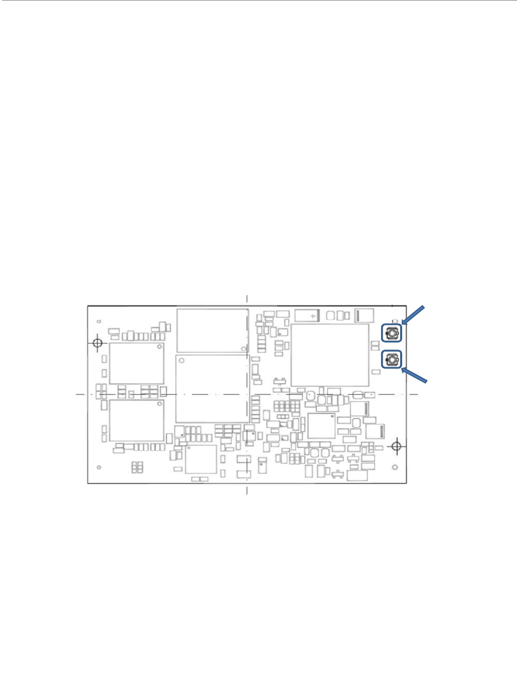
ConnectCorefori.MX51
©2010DigiInternational,Inc. 52
High-speed (with ULPI transceiver), full-speed, and low-speed operation in host mode
High-speed (with ULPI transceiver), and full-speed operation in peripheral mode
Hardware support for OTG signaling, session request protocol, and host negotiation
protocol
Up to 8 bidirectional endpoints
WLAN
WLAN
In addition to the on-module Ethernet interface, the ConnectCore for i.MX51 module can also
provide an optional 802.11a/b/g/n WLAN interface with data rates up to 54 Mbps on the
a/b/g band and up to 65 Mbps on the n band.
Two U.FL antenna connectors are provided on the module.
On the ConnectCore Wi-i.MX51 module variant, attach the antennas with the U.FL-RP-SMA
female cable to the primary connector and secondary connector on the module.
Note:
When disconnecting U.FL connectors, the use of a U.FL plug extraction tool (Hirose
P/N U.FL-LP-N-2 or U.FL-LP(V)-N-2) is strongly recommended to avoid damage to the U.FL
connectors on the module.
To mate U.FL connectors, the mating axes of both connectors must be aligned. The "click"
will confirm mated connection. Do not attempt insertion at an extreme angle.
Primary
Secondary
Secondary
ConnectCorefori.MX51
©2010DigiInternational,Inc. 53
Cable Specification: U.FL/W.FL to RP-SMA
Attributes
Dimensions
Note:
Dimensions are provided for reference purposes only. The actual antenna might vary.
1 = U.FL
2 = RP-SMA
Note:
This module obtained its complete certification by using the cable described here. End
users in North America should use a cable that matches these specs to maintain the module’s
certification.
Attribute Property
Impedance 50 Ohm
Frequency Range 0 to 6 GHz
Length 150 mm
Temperature Range -40° to +90° C
Loss 3.8dB/m (3 GHz)
5.6dB/m (6 GHz)
©2010DigiInternational,Inc. 54
About the Development Board
CHAPTER 2
The development board supports the ConnectCore for i.MX51 module. This chapter
describes the interfaces of the development board and explains how to configure the board
for your requirements.
The development board has two 180-pin connectors that mate with the module connectors.
What’s on the Development Board?
Flexible 9-30VDC charger power supply with power-on switch
Screw-flange Battery header with enable jumper
3V coin cell battery
Connectors for Digi 802.3af PoE Application board (sold separately)
1 x UART RS232 with status LEDs and SUB-D 9-pin connector
1 x UART MEI (RS232/RS4xx) with status LEDs and SUB-D 9-pin connector
1 x UART with TTL levels
1 x USB OTG connector
4 x USB Host connectors
1 x SD/MMC card holder
1 x MicroSD card holder
SPI and I2C headers
Audio interface with Line-out, Line-In and Mic-In jacks
VGA interface
HDMI interface
2 x LCD connectors with Touch Screen interface
2 x Camera connectors
RJ-45 Ethernet connector
Connector for a Digi 100M_ETHADPT (sold separately)

ConnectCorefori.MX51
©2010DigiInternational,Inc. 55
2 x RP-SMA WLAN antenna connectors
Screw-flange connector for GPIO
XBee interface (XBee module sold separately)
Peripheral application header
Module Expansion connectors
JTAG interface
2 x User LEDs (green)
2 x User Push-buttons
1 x Power down Push-button
1 x Reset Push-button
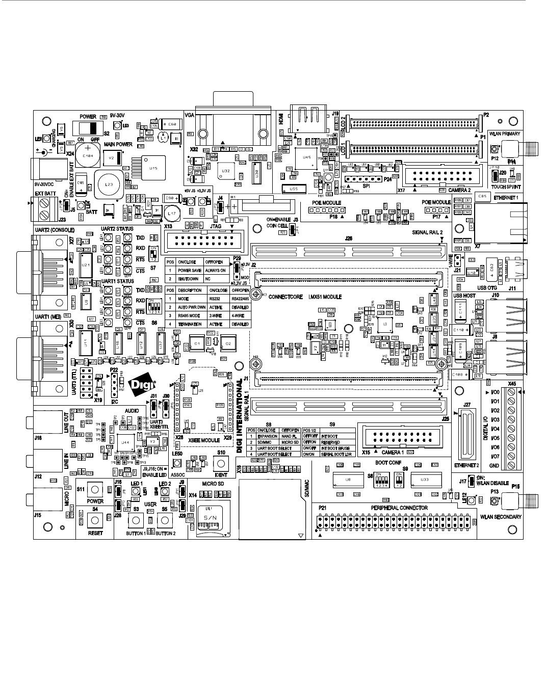
ConnectCorefori.MX51
©2010DigiInternational,Inc. 56
The Development Board
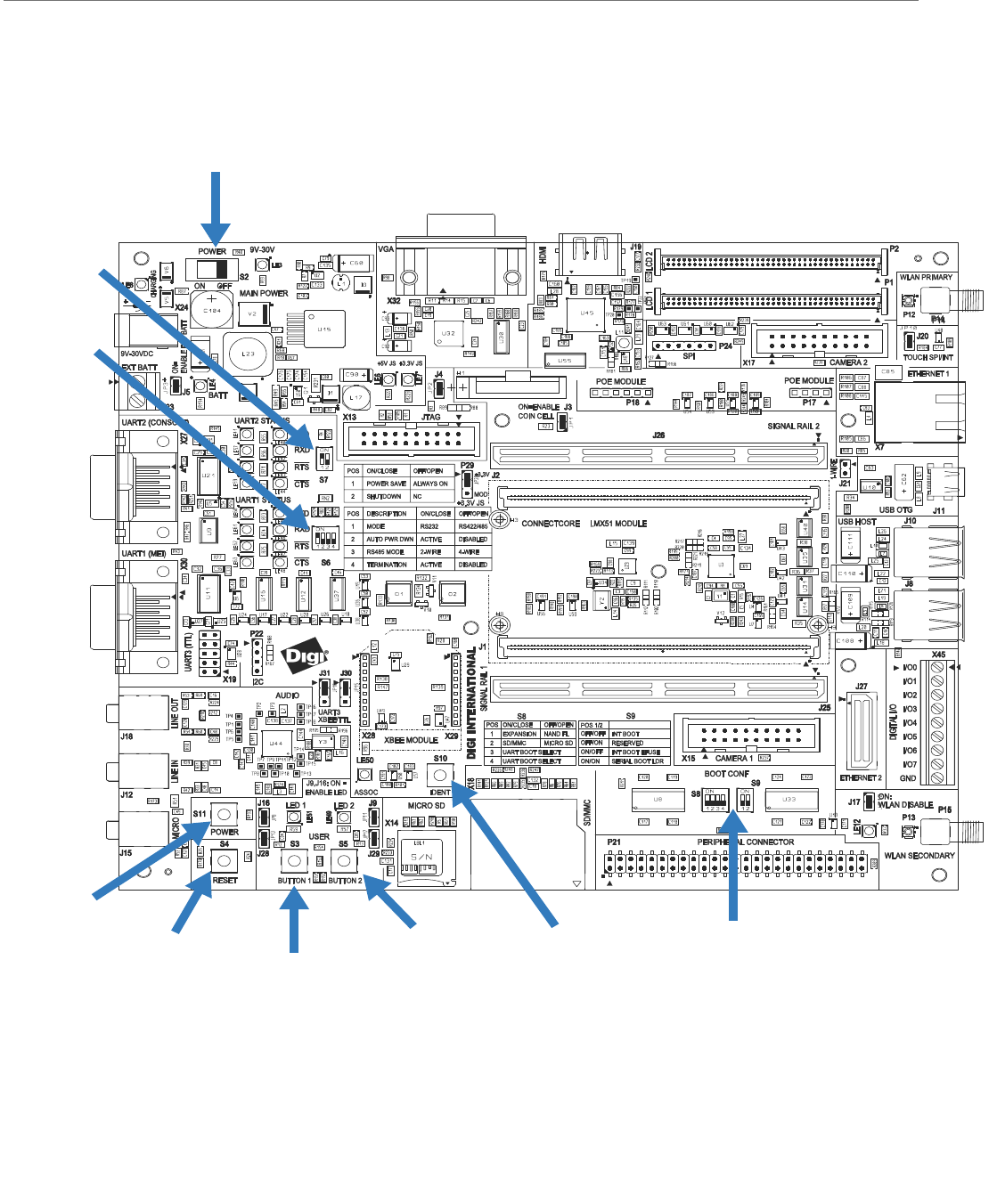
ConnectCorefori.MX51
©2010DigiInternational,Inc. 57
Switches and Push-buttons
Power Switch, S2
The development board has an ON/OFF switch, S2. The power switch S2 can switch both
9V-30VDC input power supply and 12VDC coming out of the optional PoE module. However, if
a power plug is connected to the DC power jack, the PoE is disabled.
Power Switch, S2
UART 2
Switch, S7
UART 1
Switch, S6
Power
Button, S11
Reset
Button,
S4
User
Button 1,
S3
User
Button 2,
S5
Ident
Button 1,
S10
Boot Conguration
Buttons S8, S9

ConnectCorefori.MX51
©2010DigiInternational,Inc. 58
Reset Button, S4
The reset push-button S4, resets the module and the peripherals on the development board.
A push-button allows manual reset by connecting POR# or optionally RSTIN# to ground.
Power Button, S11
The power button S11, generates a Turn On/Turn Off interrupt to the MC13892 power
management device on the module.
The Turn Off event does not directly power off the module.The module is powered off by the
processor's response to this interrupt. The software can configure a user initiated power
down, or a transition to a low power off mode by pressing this power button.
When in Off mode or in low power mode, the module can be powered via the Turn On event
generated by pressing the Power button.
User Buttons, S3 and S5
Use the user push-buttons to interact with the applications running on the ConnectCore for
i.MX51 module. Use these module signals to implement the push-buttons:
GPIO3_6 is used in User Button S3 and also in the Digital I/O connector for Digital I/O7.
Ident Button, S10
The Ident push-button S10 is associated to the commissioning input of the Digi XBee modules.
This input provides a variety of simple functions to aid in deploying devices in a network. For
a deeply description of this functionality please refer to the Digi XBee modules
documentation.
Legend for Multi-Position Switches
Switches S6, S7, S8 and S9 are multi-pin switches. In the description tables for these
switches, the position is designated as S[switch number].[pin number]. For example, position
1 on switch S6 is specified as S6.1.
Signal Name Button GPIO Used
DISPB2_SER_DIO/GPIO3_6/USER_KEY1 S3 GPIO3_8
GPIO1_1/SD1_WP#/SPI_MISO/USER_KEY2 S5 GPIO1_1

ConnectCorefori.MX51
©2010DigiInternational,Inc. 59
UART 1 Switch, S6
Use S6 to configure the line interface for serial port 1 MEI:
UART 2 Switch, S7
Use S7 to configure the line interface for serial port 2 (console):
Switch Pin Function Comments
S6.1 On = RS232 transceiver enabled
RS4xx transceiver disabled
Off = RS232 transceiver disabled
RS4xx transceiver enabled
S6.2 On = Auto Power Down enabled
Off = Auto Power Down disabled
Auto Power Down is not supported on this board.
This signal is only accessible to permit the user to
completely disable the MEI interface for using
the signals for other purposes. To disable the
MEI interface, go into RS232 mode (S6.1 = ON)
and activate the Auto Power Down feature (S1.2
= ON) - be sure that no cable is connected to
connector X30.
S6.3 On = 2-wire interface (RS4xx)
Off = 4-wire interface (RS422)
S6.4 On = Termination ON
Off = No termination
Switch Pin Function Comments
S7.1 On = Power save
Off = Normal Operation
If there is a valid RS232 signal at receiver inputs
the UART will be in normal operation mode.
If there is not a valid RS232 signal at receiver
inputs the UART will be in shutdown mode.
S7.2 On = Shutdown
Off = Normal Operation
Shutdown is the highest priority functionality. If
switch S7.2 = ON, the UART 2 will be in
shutdown mode independently of the position of
S7.1.

ConnectCorefori.MX51
©2010DigiInternational,Inc. 60
Boot Configuration Switches, S8 and S9
Use S8 to configure the source of the boot code when S9 is configures in internal boot, or to
configure the source of the serial download when S9 is configured in serial downloader.
Use S9 to configure the module boot mode:
For a detailed description of the ConnectCore for i.Mx51 boot mode functionality please
refer to the Freescale i.MX51 Processor Hardware Reference Manual.
Switch Pin Function Comments
S8.1 On = Boot from expansion device
Off = Boot from NAND Flash
Applies only if switch S9 is configured in
internal boot mode
S8.2 On = Boot from SD/MMC
Off = Boot from microSD TM
Applies only if switch S9 is configured in
internal boot mode and S8.1 is configured to boot
from expansion device
S8.3 / S8.4 On / On = UART1 (MEI) If S9 is configured in serial boot loader
S8.3 / S8.4 On / Off = UART2 (Console) If S9 is configured in serial boot loader
S8.3 / S8.4 Off / On = UART3 (TTL) If S9 is configured in serial boot loader
S8.3 / S8.4 Off / Off = Reserved If S9 is configured in serial boot loader
Switch Pin Function Comments
S9.1 / S9.2 Off / Off Internal Boot configured by switch S8
S9.1 / S9.2 Off / On Reserved
S9.1 / S9.2 On / Off Internal Boot configured by fuse block
S9.1 / S9.2 On / On Serial downloader
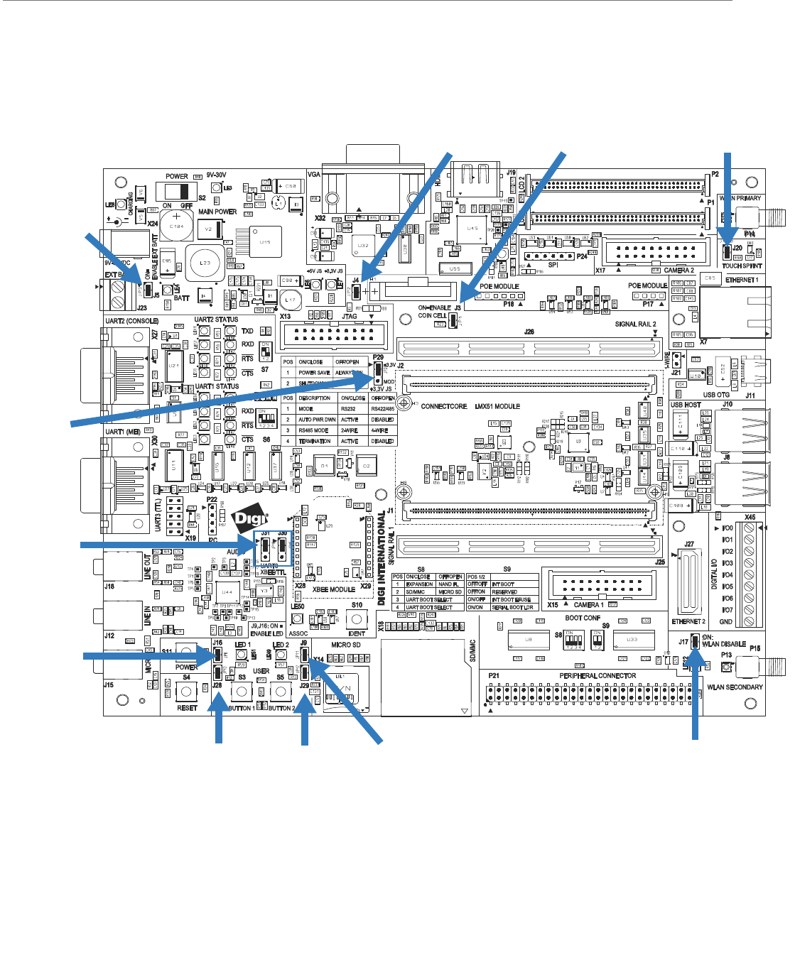
ConnectCorefori.MX51
©2010DigiInternational,Inc. 61
Jumpers
Battery Enable, J5
When J5 is set, the development board can be powered by an external battery connected to
J23.
Battery
Enable, J5
LED 1, J16
UART/XBee,
J30 & J31
WLAN Disable, J17
Module
Power
Source, P29
Button 1,
J28
LED 2,
J9
Button 2,
J29
Touch Sel, J20
Coin cell
Enable, J3
JTAG Mod, J4

ConnectCorefori.MX51
©2010DigiInternational,Inc. 62
Module Power Source, P29
When set on positions 1-2, the 3.3V supply of the development board is generated on the
+3.3V power regulator (U50).
When set on positions 2-3, the +3.3V supply of the development board is generated on the
module.
LED 1, J16
When set, enables the User LED 1 (LE51) to show the status of this signal (on if low).
LED 2, J9
When set, enables the User LED 2 (LE49) to show the status of this signal (on if low).
Button 1, J28
When set, enables the User Button 1 (S3).
Button 2, J29
When set, enables the User Button 2 (S5).
UART3 / XBee Selection, J30 and J31
The UART 3 port is shared on the development board between the XBee module socket and
the UART 3 connector (X19).
When J30 and J31 are set to positions 1-2, the UART 3 on the connector (X19) can be used.
When J30 and J31 are set to positions 2-3, the XBee module socket can be used.
WLAN Disable, J17
When set, this jumper disables the WLAN interface on the module.
Touch Selection, J20
When set, an external SPI touch screen controller is configured for the LCD 1 interface and
the internal analog touch screen controller (on module) is configured for the LCD 2 interface.
When removed, an internal touch screen controller is configured for the LCD 2 interface, and
the internal analog touch screen controller (on module) is configured for the LCD 1 interface.

ConnectCorefori.MX51
©2010DigiInternational,Inc. 63
Coincell Enable, J3
When set, this jumper supplies the real time clock with +3V from the lithium coin cell
battery, even if the board is switched off.
JTAG Mod., J4
When set, this jumper disables the JTAG interface for the ConnectCore for i.MX51.
When removed, the JTAG interface is enabled.
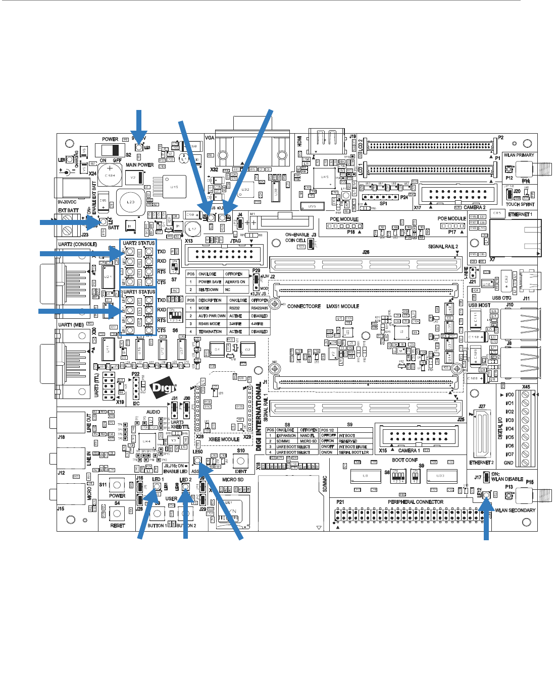
ConnectCorefori.MX51
©2010DigiInternational,Inc. 64
LEDs
WLAN, LE12
LED indicating WLAN operational status.
Batt,
LE4
WLAN, LE12
UART 2
Status
LEDs
USER LED1,
LE51
Assoc.,
LED50
USER LED2,
LE49
+3.3V_JS,
LE7
9V-30V,
LE3 +5V_JS,
LE6
UART 1
Status
LEDs

ConnectCorefori.MX51
©2010DigiInternational,Inc. 65
WLAN, LE12
LED indicating WLAN operational status.
Power LEDs, LE3, LE4, LE6 and LE7
All power LEDs are red. The power supplies must be present:
LE3 ON indicates that +9VDC / +30VDC power is present
LE4 ON indicates that battery power is present
LE6 ON indicates that +5VDC powerfor the development board is present
LE7 ON indicates that +3.3VDC power for the development board is present
User LEDs, LE49 and LE51
The user LEDs are controlled through applications running on the ConnectCore for i.MX51
module. You may use these module signals to implement the LEDs:
Serial Status LEDs
The development board has two sets of serial port LEDs - four for serial port 1 and four for
serial port 2. The LEDs are connected to the TTL side of the RS232 or RS4xx transceivers.
Green means corresponding signal high
Red means corresponding signal low
The intensity and color of the LED will change when the voltage is switching
Signal Name Button GPIO Used
NANDF_RB2/MII_COL/SP12_SCLK/GPIO3_10 LE51 GPIO3_10
NANDF_RB1/PATA_IORDY/SPI2_RDY/GPIO3_9 LE49 GPIO3_9

ConnectCorefori.MX51
©2010DigiInternational,Inc. 66
UART 1 Status LEDs
UART 2 Status LEDs
XBee Assoc., LE50
This LED is connected to the Associate output of the Digi XBee module. This LED provides
information of the device's network status and diagnostics information. For a more in-depth
description of this LED please refer to the Digi XBee modules documentation available at
www.digi.com.
LED Reference Function
RED GREEN
LE60 LE45 TXD
LE61 LE46 RXD#
LE62 LE47 RTS#
LE63 LE48 CTS#
LED Reference Function
RED GREEN
LE41 LE40 TXD
LE57 LE42 RXD
LE58 LE43 RTS#
LE59 LE44 CTS#
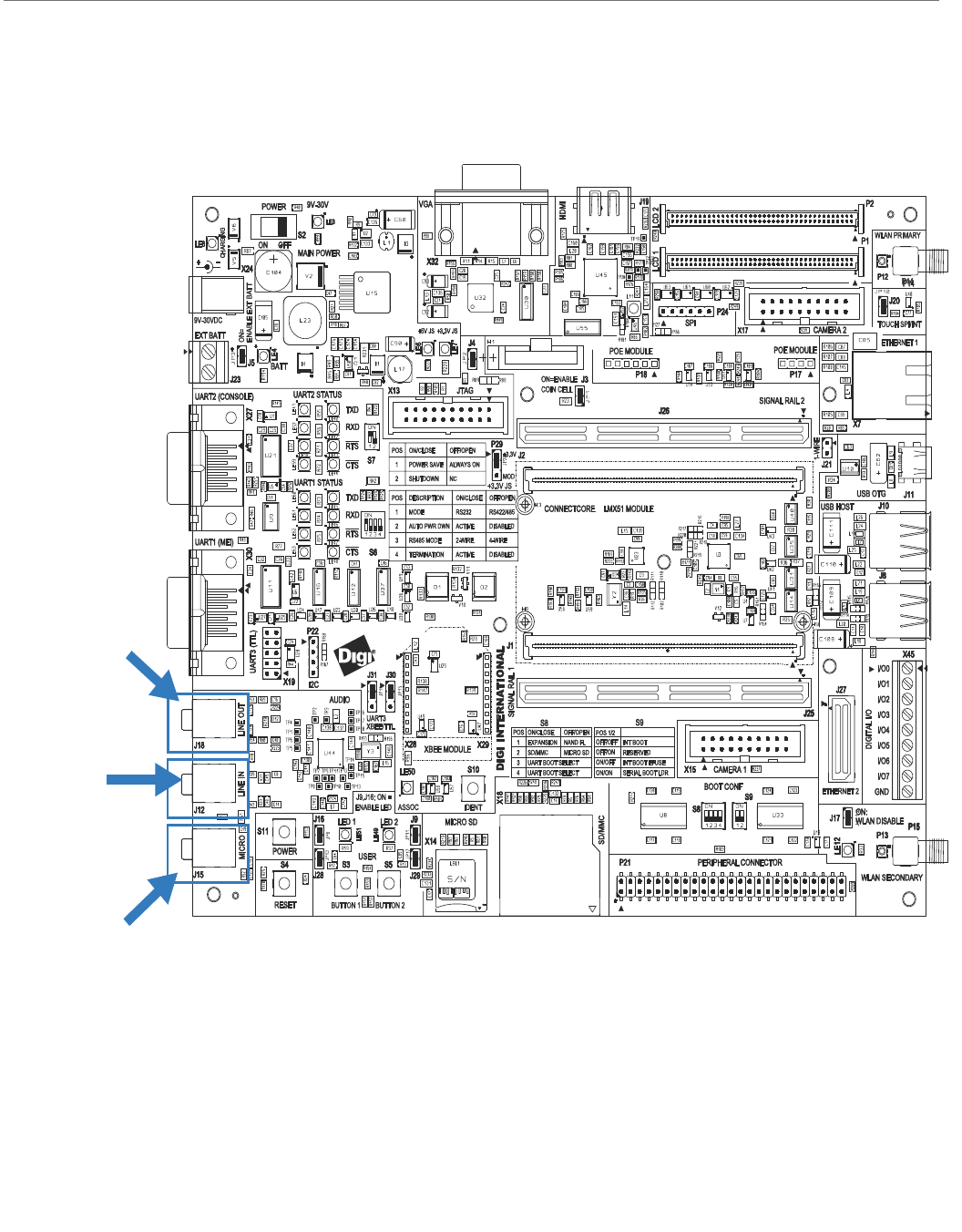
ConnectCorefori.MX51
©2010DigiInternational,Inc. 67
Audio Interface
The development board provides an audio interface with a line input channel, a line-output
channel and a microphone input. A Wolfson WM8753L audio CODEC is used in the
development board. This audio CODEC is controlled through the I2C port 2 of the
ConnectCore for i.MX51. Digital audio data is sent/received between the audio CODEC and
the ConnectCore for i.MX51 through an I2S interface (AUD3 channel of the i.MX51 AUDMUX).
Line-Out
Connector,
J18
Line-In
Connector,
J12
Micorphone
Connector,
J15

ConnectCorefori.MX51
©2010DigiInternational,Inc. 68
The I2C device address of the audio CODEC is the following:
Three stereo audio jacks are provided on the development board:
J18 connector for LINE+OUT
J12 connector for LINE+N
J15 connector for microphone
Line-out Connector Pinout, J18
Line-in Connector Pinout, J12
Microphone Connector Pinou, J15t
Interface I2C Address (7 bits)
Audio CODEC (WM8753L) 0 x 1A
Pin Signal
1GND
2LINE-OUT-RIGHT
3LINE-OUT-LEFT
4HEADPHONE-DETECT
5 -
Pin Signal
1GND
2LINE-IN-RIGHT
3LINE-IN-LEFT
4GND
5GND
Pin Signal
1GND
2MIC-IN
3MICBIAS
4GND
5GND
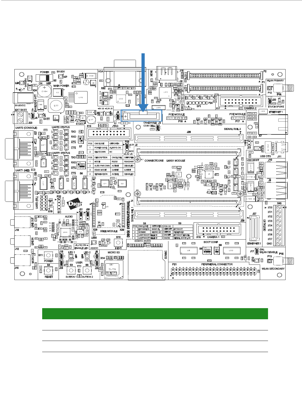
ConnectCorefori.MX51
©2010DigiInternational,Inc. 69
Coin Cell Battery
The development board provides a coin cell battery to back up the module’s integrated RTC
while main power is disconnected. Jumper J3 controls if the coin cell battery power is
available.
Battery Holder Battery
Vertical Coin-Cell Holder for CR2032 Battery Lithium coin cell, CR2032, 200mAh
Keystone 1065 Renata CR2032N
Ettinger 15.61.602 Panasonic CR2032N
Coin Cell Battery
Holder, H1
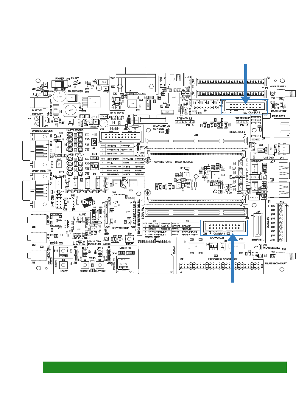
ConnectCorefori.MX51
©2010DigiInternational,Inc. 70
Camera Interfaces
The development board provides two camera interfaces connected to the camera sensor
interfaces of the ConnectCore for 1.MX51 CPU. The I2C bus of the ConnectCore for i.MX51CPU
is used to configure and control the two cameras.
The I2C device addresses of the Digi camera application kits (CC-ACC0MT9V111) are the
following:
Interface I2C Address (7 bits)
Camera 1 0 x 5C
Camera 2 0 x 48
Camera 2
Connector, X17
Camera 1
Connector, X15