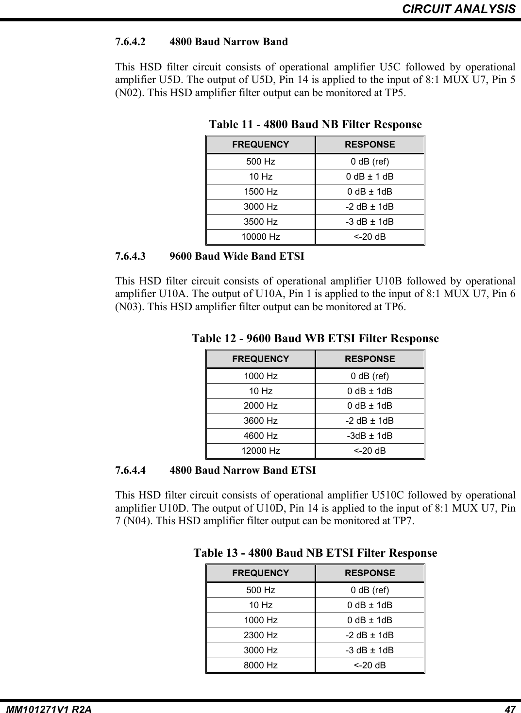
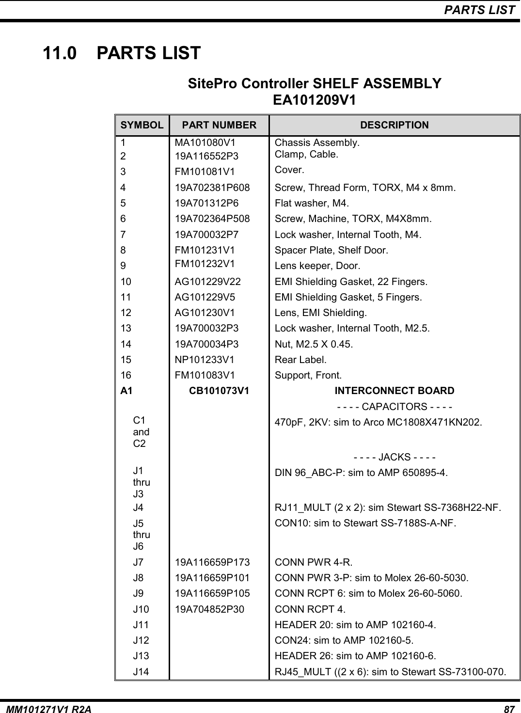
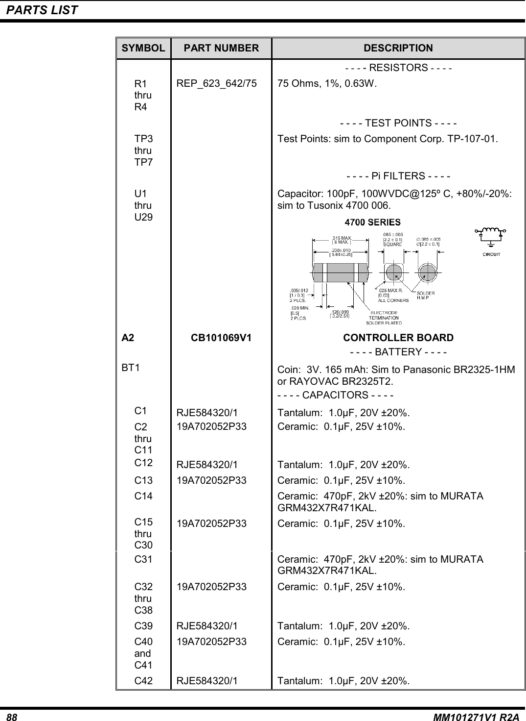
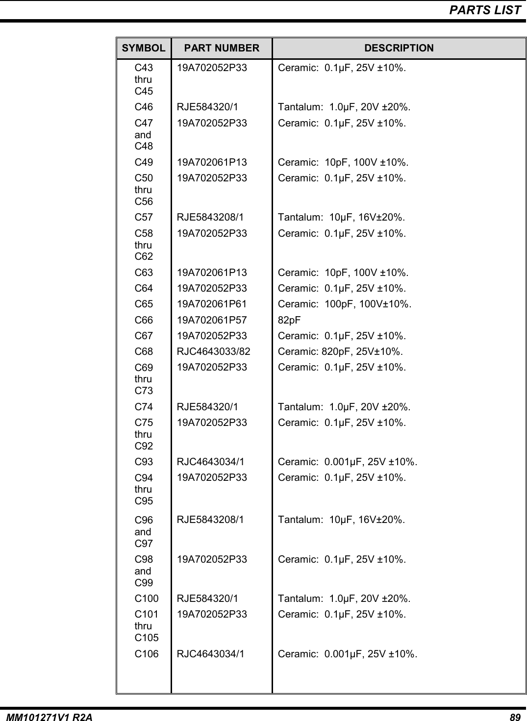
HARRIS TR-0017-E Sitepro Base Station User Manual Site Pro Manual Part 1
HARRIS CORPORATION Sitepro Base Station Site Pro Manual Part 1
UserManual.wiki
>
HARRIS
>
TR-0017-E User Manual
>
Site Pro Manual Part 1
Contents
1.
Applications Diagrams
2.
Interface Panels
3.
Main Manual
4.
Power Supply
5.
RX IF
6.
RX Synth
7.
TX Synth
8.
RF Package
9.
Site Pro Manual Part 1
10.
Site Pro Manual Part 2
Site Pro Manual Part 1
Navigation menu
Upload a User Manual
Namespaces
Wiki Guide
HTML
PDF
Info
Views
User Manual
Discussion / Help
Navigation

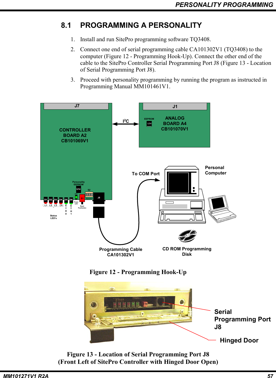
![ADDENDUM NUMBER 1 TO SITEPRO MAINTENANCE MANUALMM101271V1 R2AThis addendum adds an improved high-speed data (HSD) adjustment procedure to the following manuals:• SitePro Controller Maintenance Manual MM101271V1 R2A• SitePro Simulcast Controller Card Maintenance Manual MM101509V1 R1A• GPS Simulcast Systems (with SIM and SitePro Controllers)System Alignment and Field Testing Procedures MM101724V1 R1AThis improved procedure allows the adjustment to be made on-the-fly without the need to put the SiteProController into Test Mode. The adjustment range is the same as with the earlier procedure [two hexadecimaldigits 00-FF]. The values entered will take effect immediately. By writing these values to EEprom they willpersist through a reset. From a hyper-terminal connected to the SitePro Controller serial port1 perform thefollowing:HIGH-SPEED DATA ADJUSTMENT PROCEDUREAdjust HSD by modifying the pot setting. Once the correct level is found it must be stored in permanentmemory.1. Adjust the 'real time' high-speed level:SI2C 50 1 5 <rtn> sets slave device for all subsequent read/write operations (50 is EE pot)2. Read current data from the HSD pot:RI2C A9 A9 <rtn> reads current data at specified address range (A9 is location of the HSD pot)3. Write new values to the HSD pot. The value from step 2 provides an initial set point. The command towrite a value is:WI2C A9 xx <rtn> were xx is the hexadecimal value written to the HSD pot. Write new valuesuntil the desired deviation is achieved.4. Store the new value which achieves the desired deviation into permanent memory (novRAM) using thefollowing commands:SI2C A6 2 5 <rtn> sets slave device for all subsequent read/write operations (A6 is EEprom)WI2C 03 xx <rtn> writes new value of the HSD Pot in EEprom (03 is location of HS level)RI2C 03 03 <rtn> reads current value of the HSD Pot from EEprom (to check if writtencorrectly) 1 This procedure can also be performed through an ethernet port. Refer to the applicable manual for instructions.](https://usermanual.wiki/HARRIS/TR-0017-E.Site-Pro-Manual-Part-1/User-Guide-311120-Page-2.png)

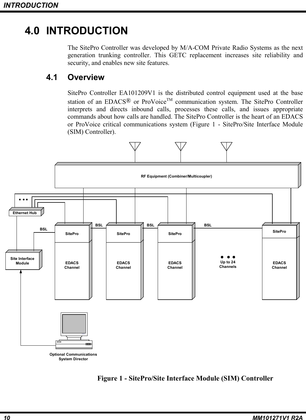

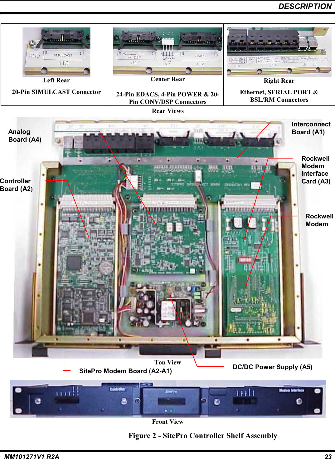
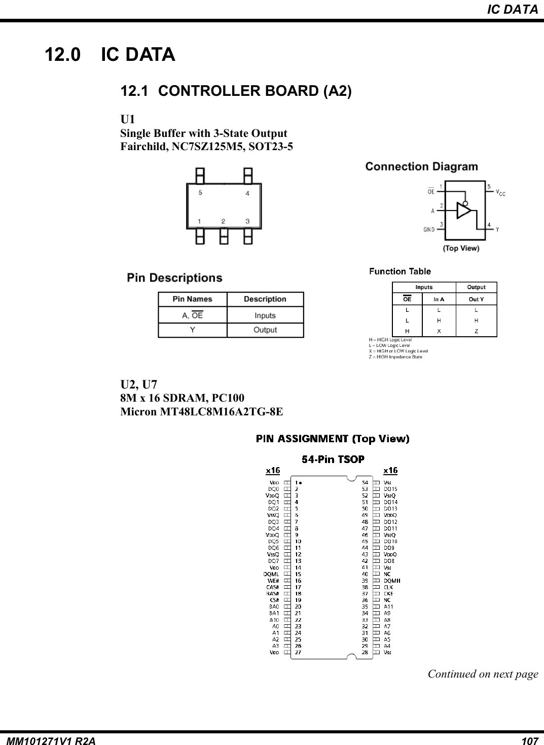
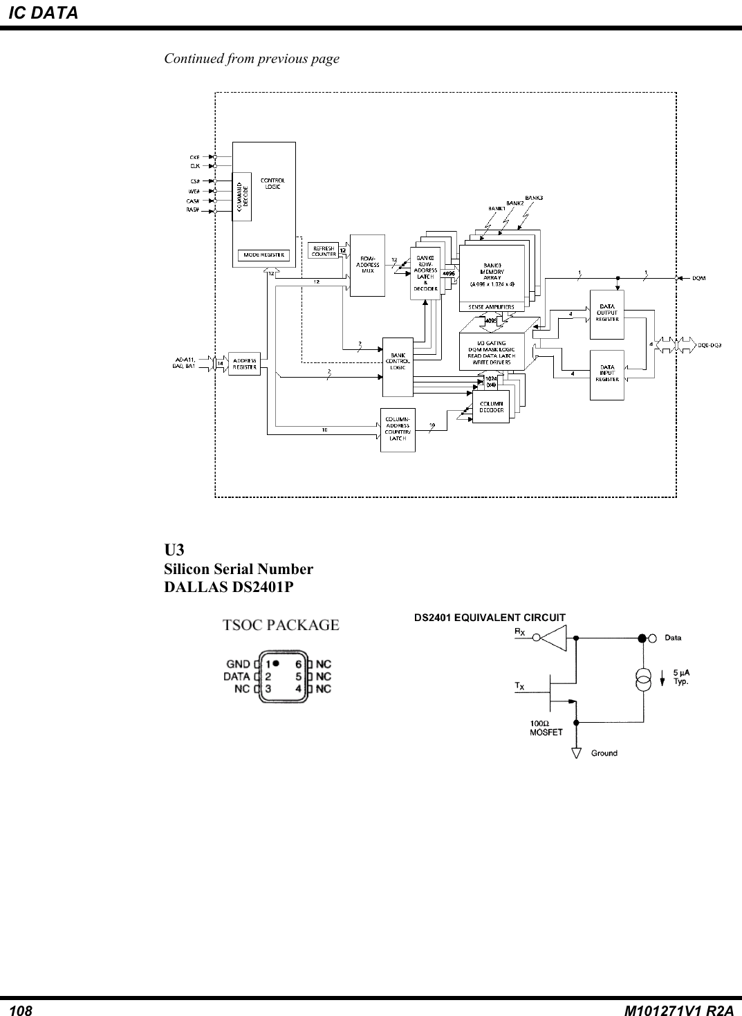
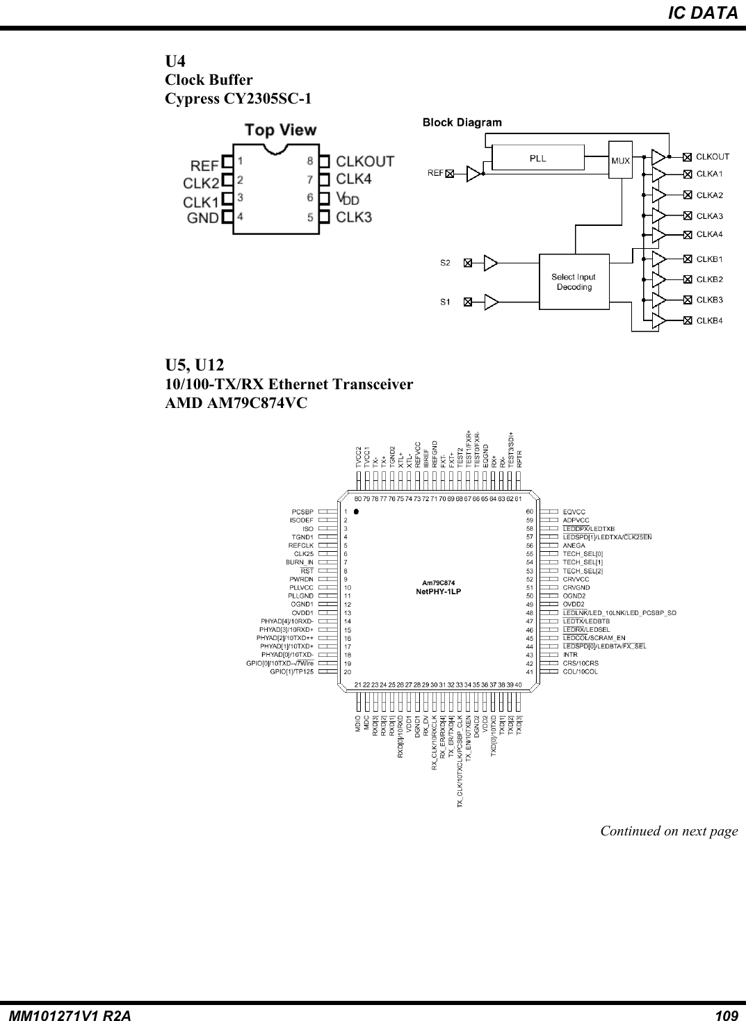
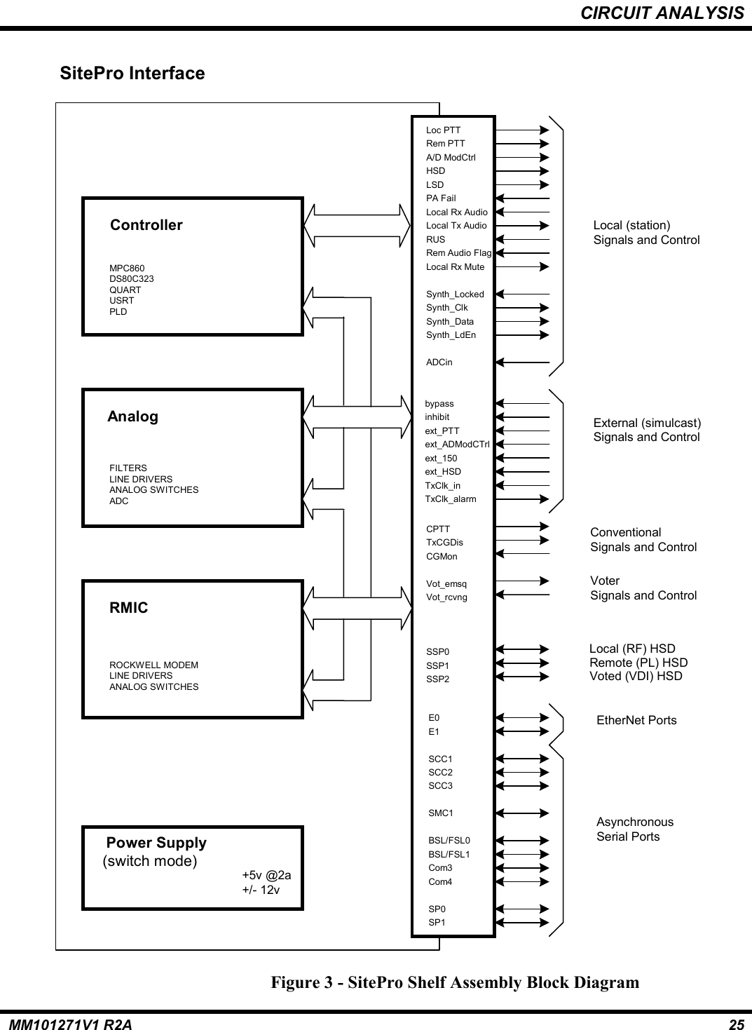
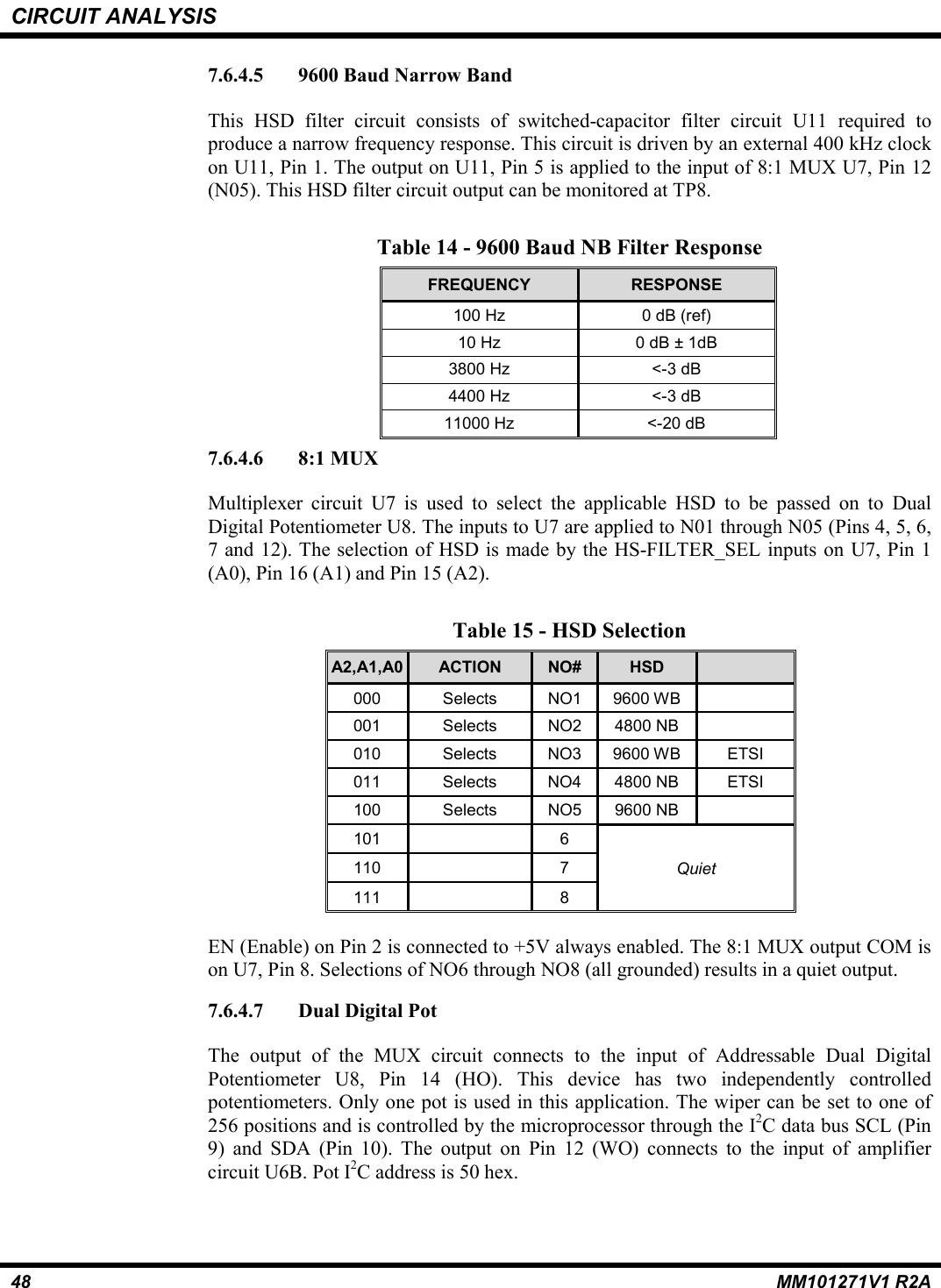
![CIRCUIT ANALYSIS24 MM101271V1 R2A7.0 CIRCUIT ANALYSISThe Theory of operation of each circuit board/card and module used in SitePro ControllerShelf Assembly EA101209V1 is described in the following paragraphs. Refer to theBlock Diagram in Figures 3 and 4 and Outline and Schematic Diagrams as listed in theTABLE OF CONTENTS.The SitePro Controller is a Base Station Controller with redundant communication links[Backup Serial Links (BSL’s)]. The BSL’s provide for inter-channel communication.Two 10Mbit Ethernet Ports provide system level communication. The BSL’s providetrunking communications as well as site configuration and database messaging. OneEthernet port is dedicated to Management System information. The second Ethernet Portis not supported at this time.The SitePro Controller and System Interface Module (SIM) will use the primary BSL fortrunking information and limited management system information. The secondary linkwill ensure continued trunking operation in the event of a primary BSL failure.The SitePro Controller/base station interface for digital information, both receive andtransmit, is 9.6k baud synchronous data. Additional digital control information isprovided via discrete I/O at both the base station and controller. The following diagram(Figure 2) is a high level picture of the SitePro Controller and external interfaces.7.1 SHELF ASSEMBLYSitePro Controller shelf Assembly EA101209V1 is a 19” Rack Mount, one Rack Unitdevice. It is enclosed to reduce emissions and interference with other devices. Serialports, Ethernet, power, and I/O connections are accessible at the back of the shelf (Figure1). The serial port connections (6 OVER 6 PHONE LINES & SERIAL PORTS) arestacked two high using RJ45 type connectors (J14) and RJ11 type connectors (J4). TheEthernet connectors J5 & J6 (ETHERNET 0 & ETHERNET 1) are single height RJ45connectors. The power connector (J7) and I/O connectors (J11, J12 & J13) are Molextype.The front panel has two hinged access doors for insertion/removal of the ControllerBoard and the Rockwell Modem card for troubleshooting and ease of maintenance. Thesedoors have RF fingers to reduce emissions. Diagnostic LEDs and the eight-characterdisplay are viewable from the front panel.The Shelf Assembly consists of Interconnect Board A1, which provides connectors toaccommodate:• Controller Board CB101069V1 (A2)• Rockwell Modem Interface Card Assembly ROA 117 2247 (A3)• Analog Board CB101070V1 (A4)• Power Supply PS101328V1 (A5)• Display Module MA101082V1 (A6)](https://usermanual.wiki/HARRIS/TR-0017-E.Site-Pro-Manual-Part-1/User-Guide-311120-Page-25.png)
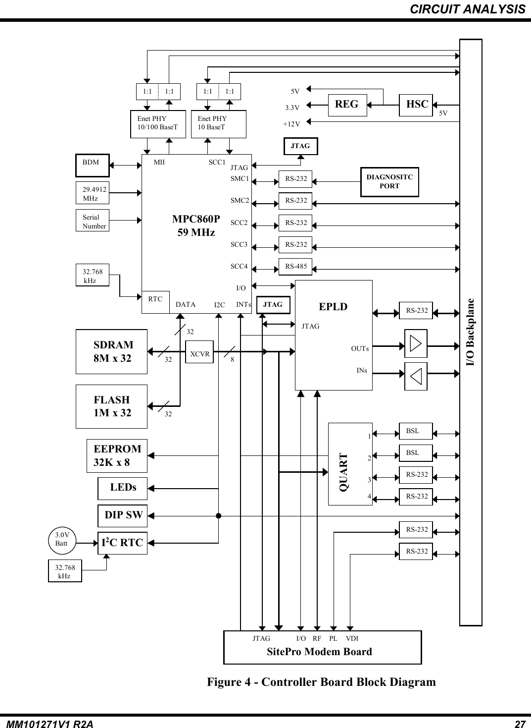
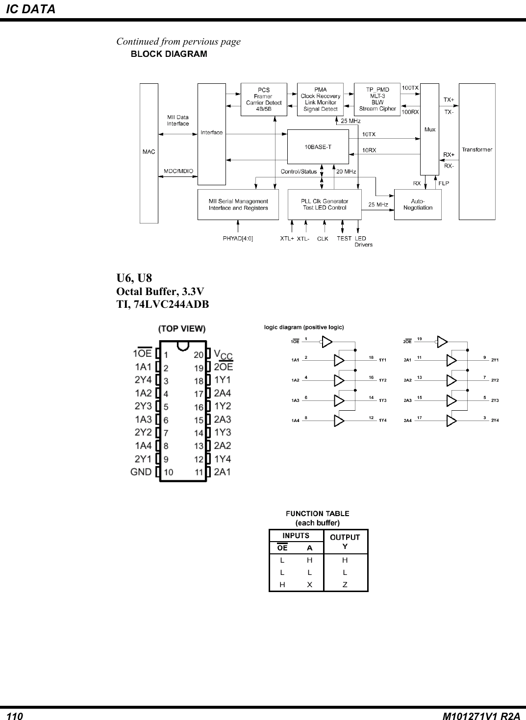
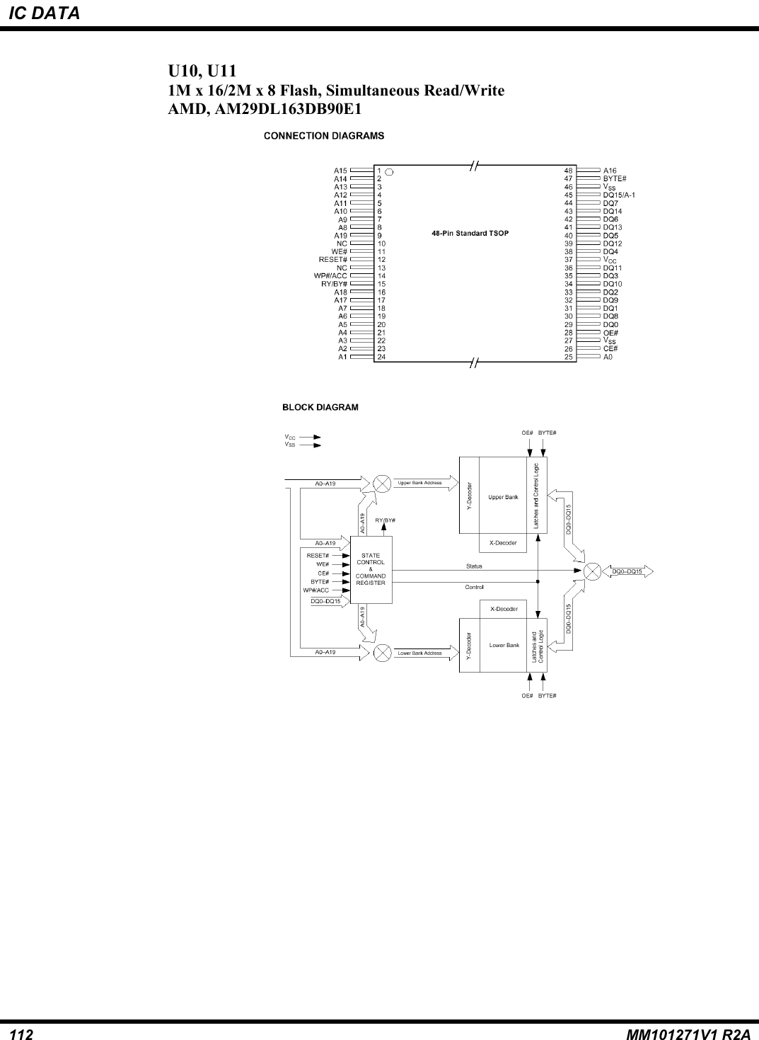
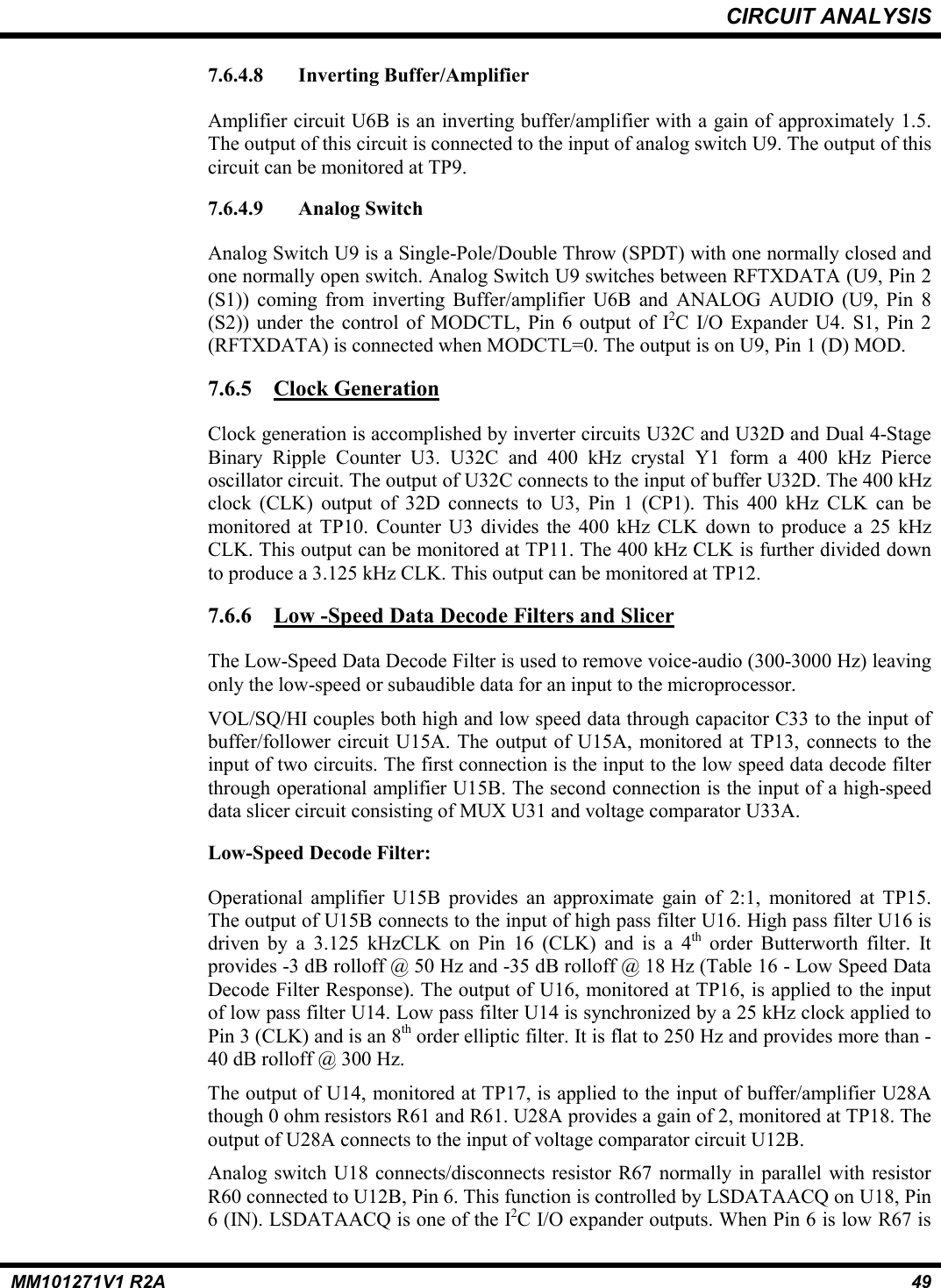
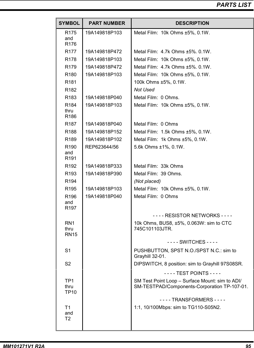
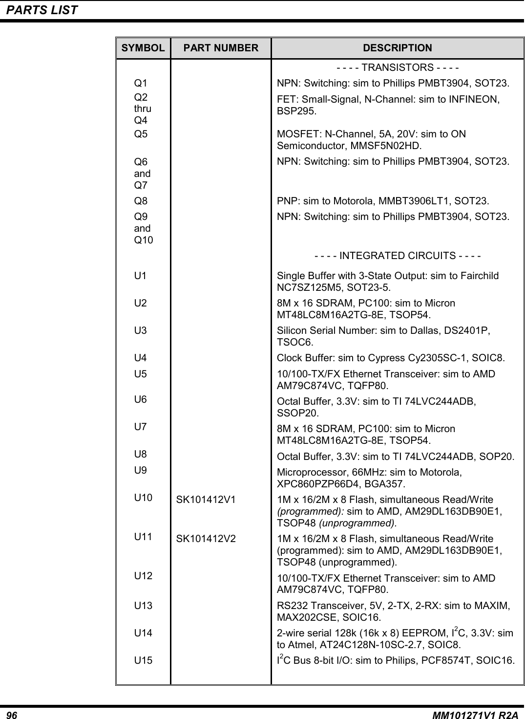
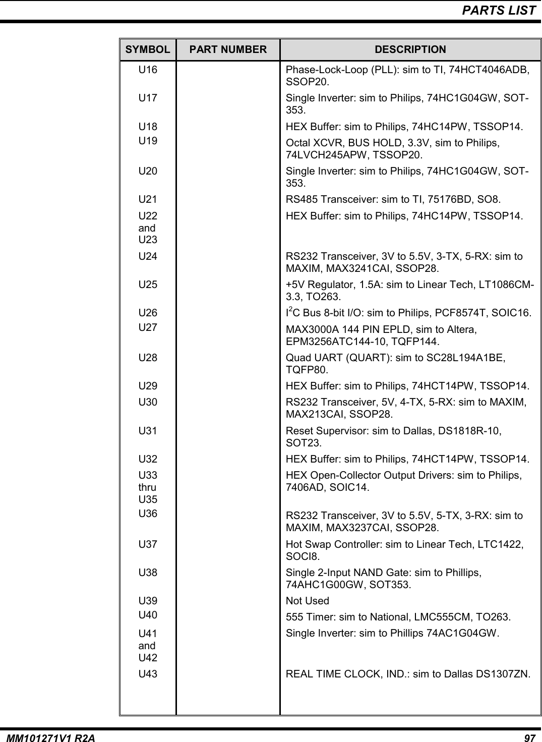
![CIRCUIT ANALYSISMM101271V1 R2A 35Table 5 - External Chip Select SignalsDEVICE IRQ MACHINE DATA BUS WIDTHFLASH CS0 GPCM 32 BitSDRAM CS1 UPMA 32 BitQUART REGISTERS CS2 GPCM 8 BitQUART INTERRUPT VECTOR CS3 GPCM 8 BitsEPLD CS4 GPCM 8 BitsMODEM DUAL PORT RAM CS5 UPMB58 BitsMODEM CODE RAM CS6 GPCM 8 Bits(SPARE-EPLD) CS7 N/A N/ANote that there is both a 32-bit data bus and an 8-bit data bus. The 8-bit data bus isconnected to the 32-bit processor data bus via an 8-bit transceiver. The output enable forthe transceiver is controlled by ANDing all 8-bit chip selects together inside the EPLD.7.3.4.2 Microprocessor SupportThe microprocessor support as shown on Schematic Diagram WP-CB101069V1, Sheet 9includes:• BDM Debug Port Connector • Silicon Serial Number• Power-On Reset Configuration • KAPWR Switch• 32 kHz Crystal • 8-Bit Bus Transceiver• VDDSYN Filter • MICTOR Logic Analyzer ConnectorsBDM Debug Port ConnectorFor debug and development, microprocessor U9A provides a dedicated serial port (BDM)for connecting a debugger/emulator. A debugger/emulator connected to this port allows aprogrammer to read/write registers and external peripherals, control program execution,etc. Many debuggers also have built-in capability to program on-board flash through thisport. These serial port pins are brought to 10-pin header J1 using the standard BDMpinout.Power-ON Reset ConfigurationThe Power-On Reset Configuration consists of four octal buffer/drivers U6A, U6B, U8Aand U8B with 3-state outputs. This circuit ensures that at Power-On all circuits are resetto the starting state. Inputs to these circuits are through 10K BUS8 resistor networks RN7and RN10. The outputs tie into bus D[0.31]. Each package is organized as two 4-bit linedrivers with separate output-enable (OE) inputs. These inputs are tied together andconnect to RESET-N. When RESET-N is low, data passes from A inputs to Y outputs.When RESET-N is high, the outputs are in the high-impedance state. This circuit imposes 5 UPMB is only required if the system makes use of the BUSY_N signal coming from the dual port memory. If BUSY_N isnot used, then a GPCM machine can be used for this chip select.](https://usermanual.wiki/HARRIS/TR-0017-E.Site-Pro-Manual-Part-1/User-Guide-311120-Page-36.png)
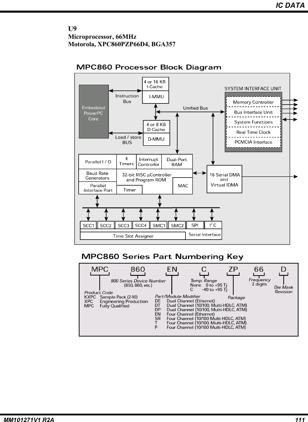
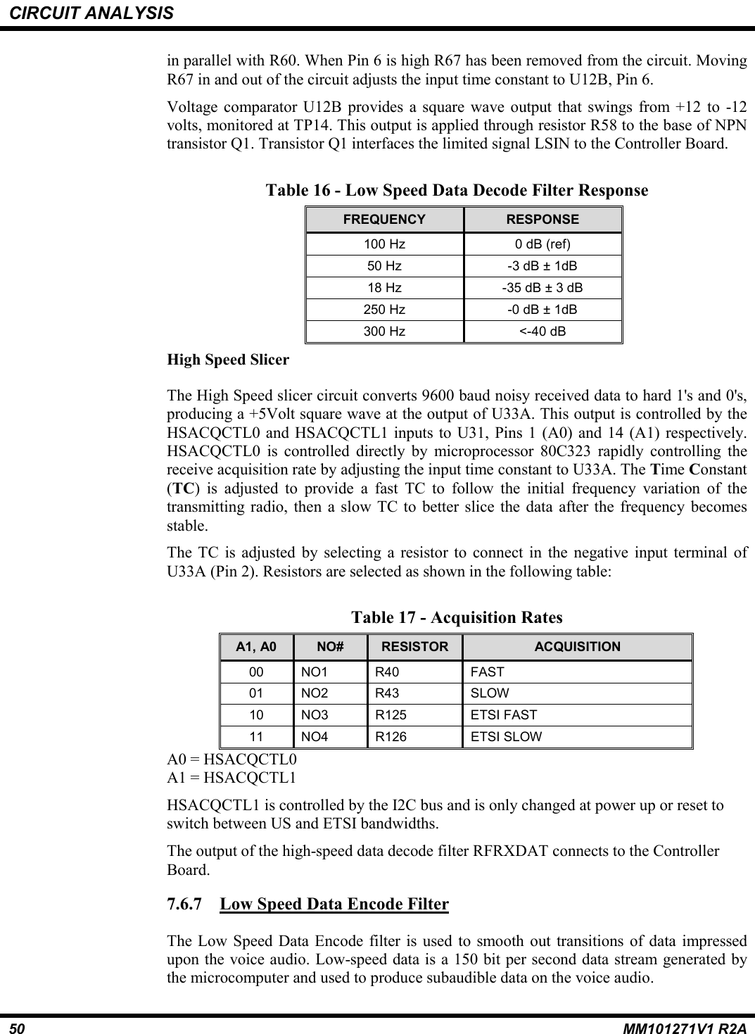
![CIRCUIT ANALYSIS36 MM101271V1 R2Apredetermined "start-up" information on the microprocessor data bus during RESET. Themicroprocessor reads the data bus state just before RESET goes inactive (high) and usesthe result for start-up initialization.At power up, the MPC860 samples the data bus and the MODCK bits to obtain theHardware Configuration Word and clock setup parameters respectively. The SiteProhardware configures these as follows:Data bus 0x017A 0000MODCK1, 2 1,0This results in the following configuration:Internal arbitrationInterrupt vector location 0xFFF0 0000Boot Port size is 32 bits.IMMR is at 0xFF00_0000.Debug Pin Configuration is as follows: VFLS[01], VF0, VF1, STS, AT1, AT2, AT0,AT3, OP3.Debug Port Pin Configuration is DSCK, DSD1, DSD0, PTR1, TCK, TD1 and TD0.External Bus speed set to ½ system clock.Pitrtc connected to extclk and div by 4, pitclk = 32.768/4 = 8192 HzSys clk connected to EXTCLK vco factor is 1, sysclk = 29.4912 MHz32 kHz CrystalThis crystal circuit consists of crystal package Y3, resistors R90 and R98, capacitors C49and C63. This circuits connects to microprocessor U9A between pins N1 (EXTAL) andP1 (XTAL) and produces an oscillator frequency of 32.768kHz to drive the real-timeclock.29 MHz ClockThe 29 MHz Clock consists of oscillator circuit Y2 and resistors R82 and R105. Thiscircuit produces the oscillator frequency of 29.4912 MHz and connects to microprocessorU9A at N2 (EXTCLK).VDDSYN FilterThis circuit consists of inductor L1 and capacitors C50 and C57. It filters the 3.3V supplyto the system Phase-Locked-Loop (PLL) circuitry on microprocessor U9A. The PLLmultiplies the EXTCLK by an integer factor to provide a bus clock.Silicon Serial NumberA unique 64-bit electronic Serial Number chip U3 is used to store the board identificationnumber. This chip has a 1-bit serial port, which interfaces to microprocessor U9 throughan I/O port. In addition, four bits of hardware identification are made available to U9through I/O ports. The Hardware ID is changed by selectively populating a bank ofresistors.](https://usermanual.wiki/HARRIS/TR-0017-E.Site-Pro-Manual-Part-1/User-Guide-311120-Page-37.png)


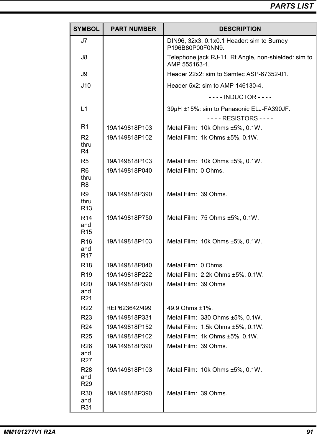
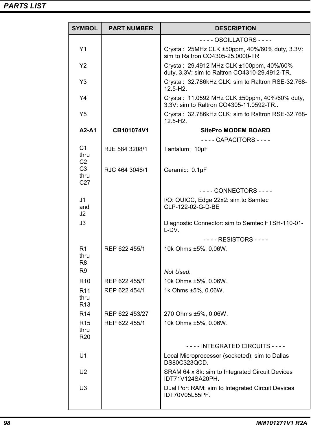
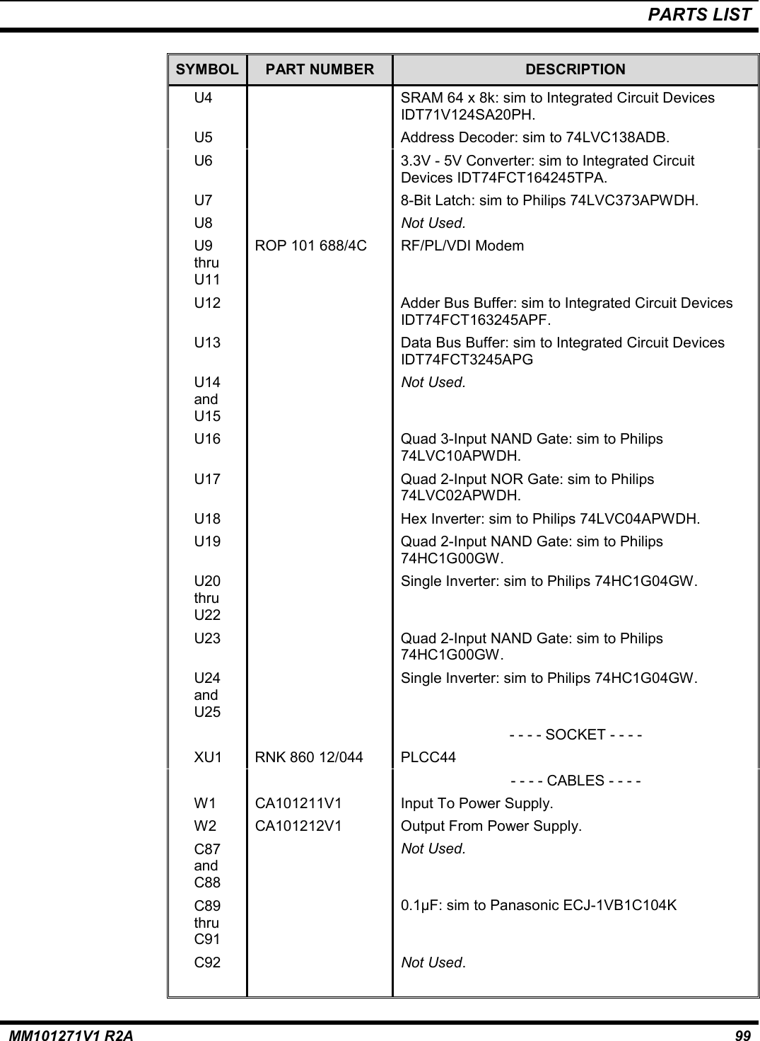
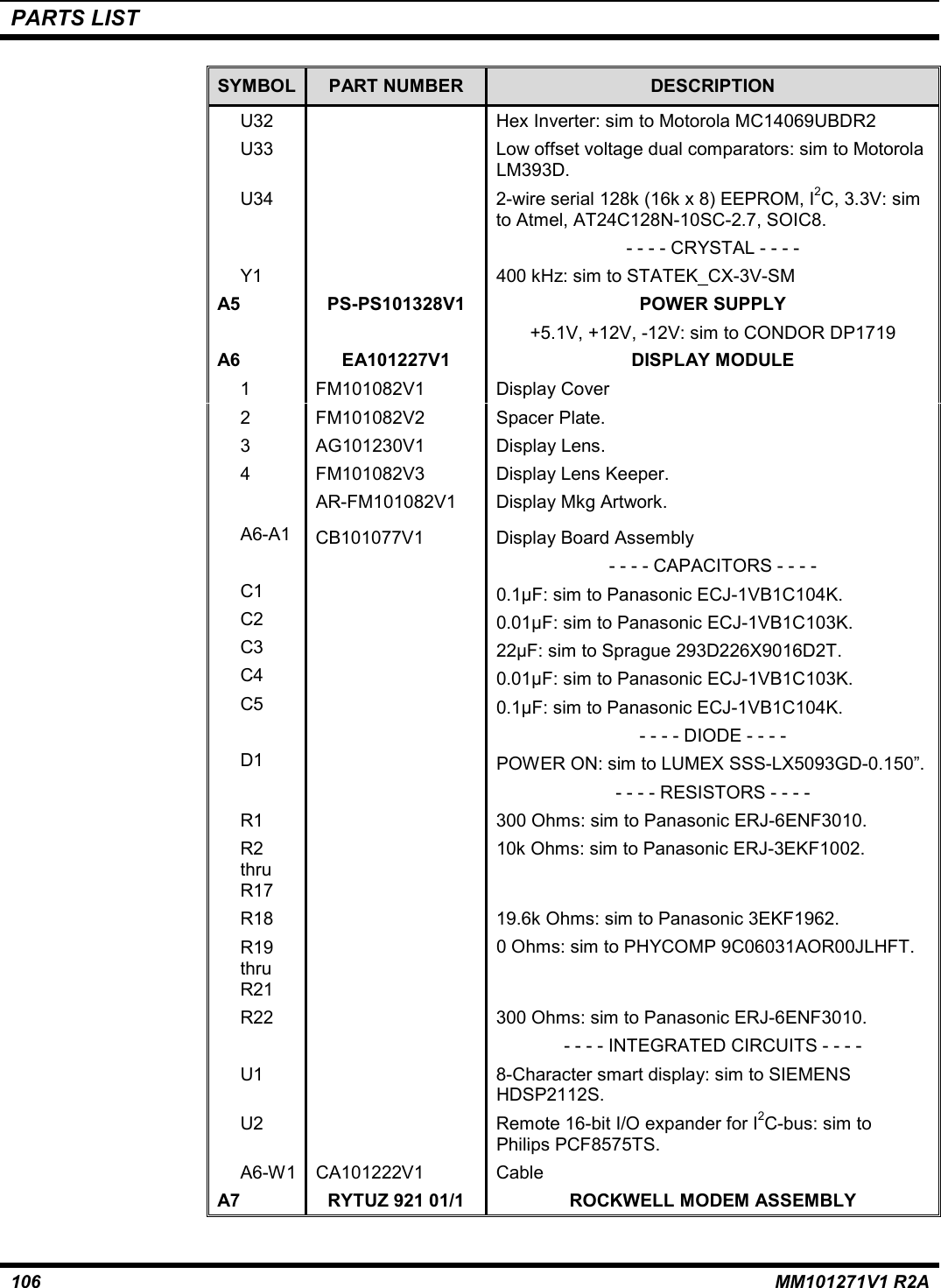
![PARTS LISTMM101271V1 R2A 101SYMBOL PART NUMBER DESCRIPTION- - - - RESISTORS - - - -R1 124k Ohms: sim to Panasonic ERJ-3EKF1243V.R2 Resistor network: SM/RP_EXB-D10C [EXB-D10C/SM]: sim to Panasonic EXB-D10C103J.R3 Not Used.R4 16k Ohms: sim to Panasonic ERJ-3EKF1602V.R5 1.21k Ohms: sim to Panasonic ERJ-3EKF1211V.R6 5.11k Ohms: sim to Panasonic ERJ-3EKF5111V.R7 1k Ohms: sim to Panasonic ERJ-3EKF1001V.R8 16k Ohms: sim to Panasonic ERJ-3EKF1602V.R9 1.21k Ohms: sim to Panasonic ERJ-3EKF1211V.R10 5.11k Ohms: sim to Panasonic ERJ-3EKF5111V.R11 1k Ohms: sim to Panasonic ERJ-3EKF1001V.R12andR13Not Used.R14 31.6k Ohms: sim to Panasonic ERJ-3EKF3162V.R15 0 Ohms: sim to Panasonic ERJ-3EKF0.0V.R16 150k Ohms: sim to Panasonic ERJ-3EKF1503V.R17 100k Ohms: sim to Panasonic ERJ-3EKF1003V.R18 1Meg Ohm: sim to Panasonic ERJ-3EKF1004V.R19 Not Used.R20 1Meg Ohms: sim to Panasonic ERJ-3EKF1004V.R21 0 Ohms: sim to Panasonic ERJ-3EKF0.0V.R22 100k Ohms: sim to Panasonic ERJ-3EKF1003V.R23andR24Not Used.R25 46.4k Ohms: sim to Panasonic ERJ-3EKF4642V.R26 0 Ohms: sim to Panasonic ERJ-3EKF0.0V.R27 100k Ohms: sim to Panasonic ERJ-3EKF1003V.R28 11k Ohms: sim to Panasonic ERJ-3EKF1102V.R29 1.96k Ohms: sim to Panasonic ERJ-3EKF1961V.R30 5.11k Ohms: sim to Panasonic ERJ-3EKF5111V.R31 1.1k Ohms: sim to Panasonic ERJ-3EKF1101V.R32 11k Ohms: sim to Panasonic ERJ-3EKF1102V.R33 1.96k Ohms: sim to Panasonic ERJ-3EKF1961V.R34 5.11k Ohms: sim to Panasonic ERJ-3EKF5111V.R35 1.1k Ohms: sim to Panasonic ERJ-3EKF1101V.R36 470 Ohms: sim to Panasonic ERJ-3EKF4700V.](https://usermanual.wiki/HARRIS/TR-0017-E.Site-Pro-Manual-Part-1/User-Guide-311120-Page-102.png)