HARRIS TR-0017-E Sitepro Base Station User Manual Site Pro Manual Part 1
HARRIS CORPORATION Sitepro Base Station Site Pro Manual Part 1
HARRIS >
Contents
Site Pro Manual Part 1

Maintenance Manual
MM101271V1 R2A
SitePro™ Controller
Shelf Assembly EA101209V1

ADDENDUM NUMBER 1 TO SITEPRO MAINTENANCE MANUAL
MM101271V1 R2A
This addendum adds an improved high-speed data (HSD) adjustment procedure to the following manuals:
• SitePro Controller Maintenance Manual MM101271V1 R2A
• SitePro Simulcast Controller Card Maintenance Manual MM101509V1 R1A
• GPS Simulcast Systems (with SIM and SitePro Controllers)
System Alignment and Field Testing Procedures MM101724V1 R1A
This improved procedure allows the adjustment to be made on-the-fly without the need to put the SitePro
Controller into Test Mode. The adjustment range is the same as with the earlier procedure [two hexadecimal
digits 00-FF]. The values entered will take effect immediately. By writing these values to EEprom they will
persist through a reset. From a hyper-terminal connected to the SitePro Controller serial port1 perform the
following:
HIGH-SPEED DATA ADJUSTMENT PROCEDURE
Adjust HSD by modifying the pot setting. Once the correct level is found it must be stored in permanent
memory.
1. Adjust the 'real time' high-speed level:
SI2C 50 1 5 <rtn> sets slave device for all subsequent read/write operations (50 is EE pot)
2. Read current data from the HSD pot:
RI2C A9 A9 <rtn> reads current data at specified address range (A9 is location of the HSD pot)
3. Write new values to the HSD pot. The value from step 2 provides an initial set point. The command to
write a value is:
WI2C A9 xx <rtn> were xx is the hexadecimal value written to the HSD pot. Write new values
until the desired deviation is achieved.
4. Store the new value which achieves the desired deviation into permanent memory (novRAM) using the
following commands:
SI2C A6 2 5 <rtn> sets slave device for all subsequent read/write operations (A6 is EEprom)
WI2C 03 xx <rtn> writes new value of the HSD Pot in EEprom (03 is location of HS level)
RI2C 03 03 <rtn> reads current value of the HSD Pot from EEprom (to check if written
correctly)
1 This procedure can also be performed through an ethernet port. Refer to the applicable manual for instructions.

2MM101271V1 R2A
NOTICE!
This manual covers products manufactured and sold by M/A-COM Private Radio Systems, Inc.
NOTICE!
Repairs to this equipment should be made only by an authorized service technician or facility designated by the supplier. Any
repairs, alterations or substitution of recommended parts made by the user to this equipment not approved by the
manufacturer could void the user's authority to operate the equipment in addition to the manufacturer's warranty.
NOTICE!
The software contained in this device is copyrighted by M/A-COM Private Radio Systems, Inc. Unpublished rights are
reserved under the copyright laws of the United States.
This manual is published by M/A-COM Private Radio Systems, Inc. without any warranty. Improvements and changes to this manual necessitated by
typographical errors, inaccuracies of current information, or improvements to programs and/or equipment, may be made by M/A-COM Private Radio
Systems, Inc., at any time and without notice. Such changes will be incorporated into new editions of this manual. No part of this manual may be
reproduced or transmitted in any form or by any means, electronic or mechanical, including photocopying and recording, for any purpose, without the
express written permission of M/A-COM Private Radio Systems, Inc.
EDACS is a registered trademark, and Aegis, ProVoice, GETC and SitePro are trademarks of M/A-COM Private Radio Systems, Inc.
Copyright 2002, M/A-COM Private Radio Systems, Inc. All rights reserved.

TABLE OF CONTENTS
MM101271V1 R2A 3
TABLE OF CONTENTS
Page
1.0 SPECIFICATIONS ................................................................................................................................................3
2.0 RELATED PUBLICATIONS................................................................................................................................3
3.0 SAFETY SYMBOLS AND INFORMATION......................................................................................................3
4.0 INTRODUCTION ..................................................................................................................................................3
4.1 OVERVIEW.............................................................................................................................................................3
4.2 OPERATIONAL FEATURES ......................................................................................................................................3
4.3 OPTIONS AND ACCESSORIES ..................................................................................................................................3
4.4 SUMMARY..........................................................................................................................................................3
5.0 MAINTENANCE AND SERVICE .......................................................................................................................3
5.1 APPLICATIONS ..................................................................................................................................................3
5.2 COMPATIBILITY AND MIGRATION ..............................................................................................................3
5.3 SYSTEM EXTERNAL INTERFACES................................................................................................................3
5.3.1 Station Control ............................................................................................................................................3
5.3.2 Simulcast Control........................................................................................................................................3
5.3.3 Conventional Control..................................................................................................................................3
5.3.4 Voter Control...............................................................................................................................................3
5.3.5 Asynchronous Serial Ports ..........................................................................................................................3
5.3.6 Synchronous Serial Ports ............................................................................................................................3
5.3.7 Power ..........................................................................................................................................................3
6.0 DESCRIPTION ......................................................................................................................................................3
6.1 INDICATORS AND CONTROLS.......................................................................................................................3
6.1.1 Indicators ....................................................................................................................................................3
6.1.2 Controls.......................................................................................................................................................3
6.2 ROCKWELL MODEM ........................................................................................................................................3
6.3 LOW SPEED AND HIGH SPEED DATA FILTERS..........................................................................................3
6.3.1 Low Speed Data Decode Filter ...................................................................................................................3
6.3.2 High Speed Data Encode Filter...................................................................................................................3
6.4 INTERFACE CONNECTIONS ...........................................................................................................................3
6.5 COMMUNICATION LINKS ...............................................................................................................................3
7.0 CIRCUIT ANALYSIS............................................................................................................................................3
7.1 SHELF ASSEMBLY ............................................................................................................................................3
7.2 INTERCONNECT BOARD (A1).........................................................................................................................3
7.3 CONTROLLER BOARD (A2).............................................................................................................................3
7.3.1 Block Diagram ............................................................................................................................................3
7.3.2 System I/O ...................................................................................................................................................3
7.3.3 Backplane....................................................................................................................................................3
7.3.4 CPU.............................................................................................................................................................3
7.3.5 SitePro Modem Board Connector ...............................................................................................................3
7.3.6 Electrically Programmable Logic Device (EPLD)......................................................................................3
7.3.7 Ethernet Ports..............................................................................................................................................3
7.3.8 I2C Bus.........................................................................................................................................................3
7.3.9 Memory........................................................................................................................................................3
7.4 SITEPRO MODEM BOARD..................................................................................................................................3
7.4.1 Modems .......................................................................................................................................................3
7.4.2 3.3V/5V Interface.........................................................................................................................................3
7.4.3 Microprocessor ...........................................................................................................................................3
7.4.4 Code Memory ..............................................................................................................................................3
7.4.5 Data Memory...............................................................................................................................................3

TABLE OF CONTENTS
4MM101271V1 R2A
TABLE OF CONTENTS
Page
7.4.6 Dual Port Ram............................................................................................................................................ 3
7.4.7 Troubleshooting Aids.................................................................................................................................. 3
7.5 ROCKWELL MODEM INTERFACE CARD (A3) ............................................................................................ 3
7.6 ANALOG BOARD (A4) ..................................................................................................................................... 3
7.6.1 Quad ADC and Single DAC ....................................................................................................................... 3
7.6.2 8-Bit I/O Expander for I2C Bus................................................................................................................... 3
7.6.3 –5 Volt Generation ..................................................................................................................................... 3
7.6.4 High-Speed Data Transmit Filters.............................................................................................................. 3
7.6.5 Clock Generation........................................................................................................................................ 3
7.6.6 Low -Speed Data Decode Filters and Slicer............................................................................................... 3
7.6.7 Low Speed Data Encode Filter................................................................................................................... 3
7.6.8 Simulcast Control Circuits.......................................................................................................................... 3
7.7 POWER SUPPLY (A5) PS101328V1 ................................................................................................................. 3
7.8 MISCELLANEOUS INFORMATION................................................................................................................ 3
7.8.1 Serial Port Data Format............................................................................................................................. 3
8.0 PERSONALITY PROGRAMMING ................................................................................................................... 3
8.1 PROGRAMMING A PERSONALITY ............................................................................................................... 3
9.0 TROUBLESHOOTING ........................................................................................................................................ 3
9.1 ON SITE TROUBLESHOOTING....................................................................................................................... 3
9.2 IN CASE OF DIFFICULTY ................................................................................................................................ 3
9.3 SITEPRO SHELF TEST...................................................................................................................................... 3
9.3.1 Equipment Needed...................................................................................................................................... 3
9.3.2 RF Data Loop Test...................................................................................................................................... 3
9.3.3 Modem Loop Test ....................................................................................................................................... 3
9.3.4 Loopback Connectors ................................................................................................................................. 3
9.4 FIELD TROUBLESHOOTING GUIDE ............................................................................................................. 3
9.4.1 SitePro Controller Board ........................................................................................................................... 3
9.4.2 SitePro Modem Board Tests From The 860 ............................................................................................... 3
9.4.3 Modem Board Tests Using Simon............................................................................................................... 3
9.4.4 Analog Board.............................................................................................................................................. 3
10.0 LIGHTNING PROTECTION GROUNDING .................................................................................................... 3
11.0 PARTS LIST .......................................................................................................................................................... 3
12.0 IC DATA................................................................................................................................................................. 3
12.1 CONTROLLER BOARD (A2)............................................................................................................................ 3
12.2 SITEPRO MODEM BOARD (A2-A1) .................................................................................................................. 3
12.3 ANALOG FILTER BOARD (A4)....................................................................................................................... 3
12.4 DISPLAY MODULE ASSEMBLY (A6) ............................................................................................................ 3
13.0 PRODUCT STRUCTURE ................................................................................................................................ 147
14.0 INTERCONNECTION DIAGRAM ................................................................................................................ 148
15.0 ASSEMBLY DIAGRAM .................................................................................................................................. 149
16.0 OUTLINE DIAGRAMS.................................................................................................................................... 150
16.1 INTERCONNECT BOARD (A1) CB101073V1............................................................................................. 150
16.2 CONTROLLER BOARD (A2) CB101069V1................................................................................................. 151
16.3 SITEPRO MODEM BOARD (A2-A1) CB101074V1 ....................................................................................... 152
16.4 ANALOG BOARD (A4) CB101070V1 .......................................................................................................... 153
16.5 DISPLAY MODULE (A6-A1) CB101077V1 ................................................................................................. 154

TABLE OF CONTENTS
MM101271V1 R2A 5
TABLE OF CONTENTS
Page
17.0 SCHEMATIC DIAGRAMS ..............................................................................................................................155
17.1 INTERCONNECT BOARD (A1) CB101073V1 .............................................................................................155
17.2 CONTROLLER BOARD (A2) CB101069V1..................................................................................................159
17.2.1 SitePro Board Title Page ........................................................................................................................159
17.2.2 Block Diagram ........................................................................................................................................160
17.3 SYSTEM I/O ....................................................................................................................................................161
17.3.1 Backplane................................................................................................................................................162
17.3.2 CPU.........................................................................................................................................................166
17.3.3 Modem Board Connector ........................................................................................................................168
17.3.4 EPLD.......................................................................................................................................................169
17.3.5 Ethernet 10 (10 Mbit PHY)......................................................................................................................170
17.3.6 Ethernet 10/100 (10/100 Mbit PHY) .......................................................................................................171
17.3.7 I2C Bus.....................................................................................................................................................172
17.3.8 Memory....................................................................................................................................................173
17.3.9 QUART ....................................................................................................................................................175
17.4 SITEPRO MODEM BOARD (A2-A1) CB101074V1........................................................................................176
17.5 ANALOG FILTER BOARD (A4) CB101070V1.............................................................................................178
17.6 DISPLAY BOARD (A6-A1) CB101077V1.....................................................................................................181
18.0 CABLE DIAGRAMS .........................................................................................................................................182
18.1 DISPLAY BOARD (A6-W1) DATA CABLE CA101222V1..........................................................................182
18.2 13.8V INPUT POWER CABLE (W1) (INPUT) CA101211V1.........................................................................183
18.3 POWER CABLE (W2) (OUTPUT) CA101212V1.............................................................................................184
18.4 ETHERNET CABLES CA101301V1 THRU V8.............................................................................................185
19.0 EPLD DRAWINGS ............................................................................................................................................186
19.1 SITEPRO TOP LEVEL ....................................................................................................................................186
19.2 LBSW ...............................................................................................................................................................187
19.3 FSL ...................................................................................................................................................................188
19.4 SYNCHRO .......................................................................................................................................................189
19.5 PIN NAMES .....................................................................................................................................................190
FIGURES
Page
Figure 1 - SitePro/Site Interface Module (SIM) Controller......................................................................................... 3
Figure 2 - SitePro Controller Shelf Assembly............................................................................................................. 3
Figure 3 - SitePro Shelf Assembly Block Diagram..................................................................................................... 3
Figure 4 - Controller Board Block Diagram................................................................................................................ 3
Figure 5 - Input Circuits U18A thru F, U22B thru D and U23C thru F....................................................................... 3
Figure 6 - Input Circuits U22A, E, F, U29D and U32B .............................................................................................. 3
Figure 7 - Output Circuits U29B, C, E & F, U33C, E & F and U34A thru F.............................................................. 3
Figure 8 - Output Circuits U33B, C, E, F, U34A, B, C, D, E, F and U35C, D, E & F................................................3
Figure 9 - Site Pro Modem Board Block Diagram ...................................................................................................... 3
Figure 10 - I2C Address............................................................................................................................................... 3
Figure 11 - Analog Board Block Diagram................................................................................................................... 3
Figure 12 - Programming Hook-Up ............................................................................................................................ 3
Figure 13 - Location of Serial Programming Port J8 (Front Left of SitePro Controller with Hinged Door Open) ..... 3
Figure 14 - RF Data Signal Path.................................................................................................................................. 3
Figure 15 - Phone Line Data Signal Path .................................................................................................................... 3
Figure 16 - Loopback Test Connectors ....................................................................................................................... 3

TABLE OF CONTENTS
6MM101271V1 R2A
TABLE OF CONTENTS
Page
TABLES
Table 1 –Asynchronous Serial Ports............................................................................................................................3
Table 2 - Synchronous Serial Ports..............................................................................................................................3
Table 3 - Interface Connections...................................................................................................................................3
Table 4 - External Processor Interrupt Signals ............................................................................................................3
Table 5 - External Chip Select Signals ........................................................................................................................3
Table 6 - 10 Mbit Ethernet Connections......................................................................................................................3
Table 7 - I2C Bus Addresses ........................................................................................................................................3
Table 8 - DRAM Bank Memory Ranges ..................................................................................................................... 3
Table 9 - Memory Map................................................................................................................................................ 3
Table 10 - 9600 Baud WB Filter Response .................................................................................................................3
Table 11 - 4800 Baud NB Filter Response ..................................................................................................................3
Table 12 - 9600 Baud WB ETSI Filter Response ........................................................................................................3
Table 13 - 4800 Baud NB ETSI Filter Response.........................................................................................................3
Table 14 - 9600 Baud NB Filter Response ..................................................................................................................3
Table 15 - HSD Selection ............................................................................................................................................3
Table 16 - Low Speed Data Decode Filter Response ..................................................................................................3
Table 17 - Acquisition Rates .......................................................................................................................................3
Table 18 - Low-Speed Data Encode Filter Response ..................................................................................................3
Table 19 -Minimum Operating System Requirements ................................................................................................3
Table 20 - Cable Connections......................................................................................................................................3
Table 21 - Current (I) Limits .......................................................................................................................................3
Table 23 - SIMON Commands....................................................................................................................................3
Table 24 - I/O Signal Paths..........................................................................................................................................3
Table 25 - FactoryTest Manual Mode Commands ......................................................................................................3
Table 26 - I/O Output Group A Paths..........................................................................................................................3
Table 27 - FactoryTest Manual Mode Commands (Group B).....................................................................................3
Table 28 - I/O Outputs Group B Paths.........................................................................................................................3
Table 29 - FactoryTest Manual Mode Commands (Group C)..................................................................................... 3
Table 30 - I/O Outputs Group C Paths......................................................................................................................... 3
Table 31 - FactoryTest Command Mode READ Commands ...................................................................................... 3
Table 32 - Group A I/O Input Paths.............................................................................................................................3
Table 33 - READ Commands and Expected Results................................................................................................... 3
Table 34 - I/O Input Group B Paths.............................................................................................................................3
Table 35 - Test Point Levels........................................................................................................................................3
Table 36 - Frequency Response at LSDTX .................................................................................................................3
Table 37 - Circuit Levels .............................................................................................................................................3
Table 38 - High Speed Data Signal Levels..................................................................................................................3

SPECIFICATIONS
MM101271V1 R2A 7
1.0 SPECIFICATIONS1
INPUT VOLTAGE +13.8±20% VDC
CURRENT DRAIN
Without 9600 baud modem 900mA (typical), 1.5 Amps (maximum)
With 9600 baud modem 1.5 Amps (typical), 2 Amps (maximum)
OPERATING TEMPERATURE -22°F to +140°F (-30°C to +60°C)
DIMENSIONS (H x W x D) 1.75 x 17.12 x 15.625 inches
(4.44 x 43.48 x 39.69 cm)
DATA TRANSMISSION
High Speed (RF and phone line) 9600 ±1bps (EDACS Wideband)
Low Speed 150 ±1bps
COMMUNICATION INTERFACE
Redundant Communication Link
Data Levels 0 to 13.8 VDC (nominal)
Data Format 1 start bit, 1 stop bit, and 8/9 data bits
Data Rate 38.4 kbaud
Ethernet Interfaces 10 Mbit
1 These specifications are intended to be used by the service technician during servicing. Refer to the appropriate
Specification Sheet for the complete Specification.

RELATED PUBLICATIONS
8MM101271V1 R2A
2.0 RELATED PUBLICATIONS
Publication Title
LBI-39152 Rockwell Modem Interface Card ROA 117 2247/1
Rockwell Modem Assembly, RYTUA 921 01/1
RS-232 INTERFACE CARD, ROA 117 2247/2
MM101343V1 SitePro Controller Installation and Configuration Manual
MM101461V1 SitePro Personality Programming Manual
SAFETY SYMBOLS
MM101271V1 R2A 9
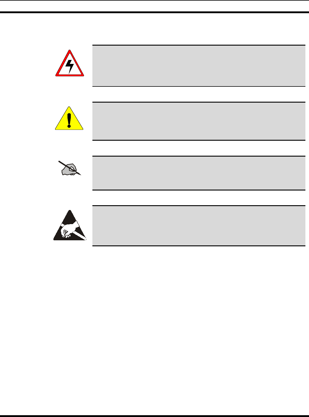
3.0 SAFETY SYMBOLS AND INFORMATION
WARNING
The WARNING symbol calls attention to a procedure, practice, or the like,
which, if not correctly performed or adhered to, could result in personal
injury. Do not proceed beyond a WARNING symbol until the conditions
identified are fully understood or met.
CAUTION
The CAUTION symbol calls attention to an operating procedure, practice, or
the like, which, if not performed correctly or adhered to, could result in
damage to the equipment or severely degrade the equipment performance.
NOTE
The NOTE symbol calls attention to supplemental information, which may
improve system performance or clarify a process or procedure.
The ESD symbol calls attention to procedures, practices, or the like, which
could expose equipment to the effects of Electro-Static Discharge. Proper
precautions must be taken to prevent ESD when handling circuit modules.
• The means of disconnecting power from a station cabinet is the cabinet power supply
plug.
• When conducting repair/maintenance, disconnect the cabinet power supply plug from
the AC source.
• In European applications, equipment must be installed in a closed cabinet.
• Only replace components with components specified by M/A-COM Private Radio
Systems.
INTRODUCTION
10 MM101271V1 R2A
4.0 INTRODUCTION
The SitePro Controller was developed by M/A-COM Private Radio Systems as the next
generation trunking controller. This GETC replacement increases site reliability and
security, and enables new site features.
4.1 Overview
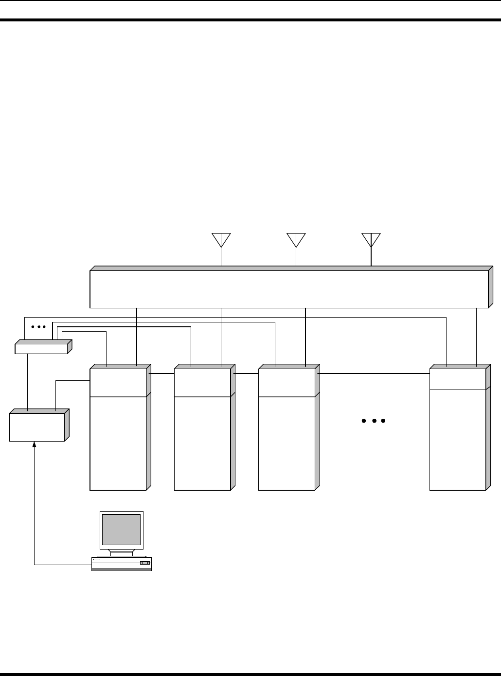
SitePro Controller EA101209V1 is the distributed control equipment used at the base
station of an EDACS® or ProVoiceTM communication system. The SitePro Controller
interprets and directs inbound calls, processes these calls, and issues appropriate
commands about how calls are handled. The SitePro Controller is the heart of an EDACS
or ProVoice critical communications system (Figure 1 - SitePro/Site Interface Module
(SIM) Controller).
SitePro
EDACS
Channel
SitePro
EDACS
Channel
SitePro
EDACS
Channel
SitePro
EDACS
Channel
BSL BSL BSL
RF Equipment (Combiner/Multicoupler)
Up to 24
Channels
~V.T
Optional Communications
System Director
Ethernet Hub
Site Interface
Module
BSL
Figure 1 - SitePro/Site Interface Module (SIM) Controller

INTRODUCTION
MM101271V1 R2A 11
4.2 Operational Features
The CSD allows access to the user and site database utilized by the SitePro Controller.
The SitePro Controller offers the following features:
1. Eight Priority Levels – The SitePro Controller prioritizes calls from a list of
individual and group identification numbers (LIDs and GIDs) for use during queuing.
This prioritized list ensures that higher priority calls are processed first for critical
communications.
2. Call Validation – The SitePro Controller checks the ID of every radio attempting to
access the system. An invalid ID attempting to use the system will be denied access,
eliminating system security breeches.
3. Unit Enable/Disable – The SitePro Controller has the capability to disable and
enable radios over the air. This feature prevents intruders from accessing the system
with stolen or misplaced radios.
4. Dynamic Regroup – This feature allows the SitePro Controller to reconfigure radio-
operating groups in response to critical emergency situations.
5. Recent Priority Increments – The SitePro Controller is able to increase the priority
level of ID’s that have recently placed calls. This allows ongoing conversations to
have a higher priority.
6. Local Telephone Interconnect – The SitePro Controller supports local telephone
interconnect. Calls can be made to and from an individual or to a group in an EDACS
or ProVoice system.
7. Multiple Channel Partition (MCP) – Using MCP, the SitePro Controller is capable
of segregating sets of channels for exclusive use by select users. Up to 15 distinct
partitions may be defined to ensure channel availability for critical communications.
8. Toll Call Restriction - The SitePro Controller is able to restrict Hotline telephone
access by radio for both local and long distance calls.
9. Patch and Simulselect - The SitePro Controller allows console dispatchers to
"patch" together different talkgroups. This feature allows maximum response to
emergency situations.
10. Site Configuration - The SitePro Controller is the repository for critical site
configuration data resident on the Communications Systems Director (CSD).
11. Redundant Downlink GETCTM (Optional) - A Downlink GETC shelf provides the
9600-baud Integrated Multisite and Console Controller (IMC) link for
communications control from the repeater site to the dispatch center site or multisite
switch.
4.3 Options and Accessories
Site Sentry Alarm and Control System – The Site Sentry alarm and control equipment
enables the SitePro Controller to monitor key aspects of the site operation, including the
following:
1. Remote reporting of inputs from customer-specific alarm sensors.
2. Remote control of relays that operate customer-specific devices.

INTRODUCTION
12 MM101271V1 R2A
3. Diagnostic testing of system operation.
4. Local display of system status
The Site Sentry also keeps track of transmitter performance and the antenna system. The
parameters monitored to verify the system health are transmitter power, forward and
reflected antenna power, and antenna Voltage Standing Wave Ratio (VSWR).
Site SureCall Test Call System – Site SureCall allows remote channel monitoring and
testing of repeater stations via a Test Unit (TU) radio.
Hotline Local Telephone Interconnect – The SitePro Controller provides the processing
for Hotline. Calls can be made from the Public Switched Telephone Network (PSTN) to
an individual or group as well as from a radio to the PSTN.
4.4 SUMMARY
The SitePro Controller provides the latest control technology to ensure that the EDACS
or ProVoice critical communication system is unmatched in system performance. The
SitePro Controllers are capable of maintaining the following critical communication
features even if the SIM, due to a temporary failure, is taken out or service:
1. Eight Priority Levels
2. Call Validation
3. Recent Priority Increment
4. Multiple Channel Partition
5. Patch and Simulselect

MAINTENANCE AND SERVICE
MM101271V1 R2A 13
5.0 MAINTENANCE AND SERVICE
This manual provides maintenance and servicing information for M/A-COM SitePro
Controller Shelf Assembly EA101209V12. Production versions of this shelf consist of the
following components:
• Shelf Assembly MA101080V1
• Interconnect Board Assembly (A1) CB101073V1
• Controller Board Assembly (A2) CD101069V1
• SitePro Modem Board (A2-A1) CB101074V1
• Rockwell Modem Interface
Card Assembly (A3) ROA 117 2247
Rockwell Modem Assembly (A7) RYTUZ 921 01/1
• Analog Board (A4) CB101070V1
• Power Supply Module (A5) PS-PS101328V1
• Display Module (A6) MA101082V1
Display Board Assembly (A6-A1) CB101077V1
Cable (A6-W1) CA101222V1
• Input Cable to the Power Supply (W1) CA101211V1
• Output Cable from the Power Supply (W2) CA101212V1
5.1 APPLICATIONS
The SitePro Controller can be installed and configured for several different station
applications. Initially the basic configuration is for the EDACS Station Trunking Shelf.
This shelf enables the station to function as part of an EDACS trunked communication
system by providing digital signaling and control of the associated base station. In
addition, the SitePro Controller provides an interface between the base station repeater,
the Site Interface Module (SIM) and other channel SitePro Controller(s) at the same
time.
5.2 COMPATIBILITY AND MIGRATION
The SitePro Controller, with the exception of the Site Controller, is compatible with
GETC compatible devices as follows:
• Downlink GETC
• SIM
• SureCall
• Hotline
• Site Sentry
2 The Service Technician(s) should always consult any application manuals, Software Release Notes (SRN), and Specific
Customer information provided with the system whenever the equipment requires service or repair.

MAINTENANCE AND SERVICE
14 MM101271V1 R2A
The requirements for compatibility and migration are that:
1. The SitePro Controller will only switch modes if the Control Channel fails or a
configuration command is received. The SitePro Controller will, however, change
modes as currently implemented by the GETC. For example, the SitePro Controller
Control Channel can switch modes, without failure or configuration command, if it
detects carrier.
2. For High Speed Data Modulation, the SitePro Controller has a separate Analog Board
(A4) providing software configurable filtering, which is compatible with high-speed
data types.
5.3 SYSTEM EXTERNAL INTERFACES
(SitePro Trunked Interface Specification)
The following is a description of all electrical connections to the SitePro Controller. All
input/output definitions are relative to the SitePro Controller. This configuration supports
EDACS, Simulcast and Voted systems. The analog and digital control signals provide an
interface to a variety of base stations and are grouped by functionality.
5.3.1 Station Control
• LocRxAudio - Analog input
MASTR III level = 1 Vrms, Zin = 100Kohm, bias = ac coupled
This signal is unfiltered local receiver audio from the base station also called
Volume/Squelch or VolSqHi and carries either High Speed Data (control
signaling/digital audio) or Low Speed Data with analog audio. The two components
are internally separated.
• RUS - Digital TTL active high input
This signal is the Receiver UnSquelch signal from the base station and is activated
when a carrier of sufficient signal strength (as determined by the squelch pot setting)
is present.
• LSD - Analog output
level = 300 mVrms
Zout = 100ohm, bias = 0 volts
This signal is the Low Speed Data output to the base station. The signal is
conditioned through a low pass filter to remove frequency components above 300 Hz
to allow multiplexing with analog voice audio.
• HSD - Analog output
level = 1.1 Vrms
Zout = 100ohm, bias = 0 volts
This signal is the High Speed Data output to the base station modulator. The signal is
conditioned through a specially designed filter needed to meet precise RF modulation
bandwidth limitations.

MAINTENANCE AND SERVICE
MM101271V1 R2A 15
• LocPTT - Digital active low open drain output
This signal is the Local PTT control. This line, when low, will key up the base station
transmitter and select the local receiver audio source for transmission.
• RemPTT - Digital active low open drain output
This signal is the Remote PTT control. This line, when low, will key up the base
station transmitter and select the remote audio source for transmission.
• A/DmodCtrl - Digital output TTL
This is the Analog/Digital Modulation Control signal. When high, HSD is routed to
the base station transmit. When low, LSD/audio is routed to the base station transmit.
• HSAcq - Digital output open drain output
This is the High-Speed Acquisition control signal. A high or low signal produces a
corresponding high or low time constant in the limiter circuit.
• LocRxMute - Digital active low output (8.5 volt low Z source)
This signal is the Local Receiver Mute control. This line, when low, blocks the
routing of receiver audio to the base station transmitter and line out. Muting occurs
during HSD transmission, no valid carrier present, or no valid LSD present.
• Walsh1/Walsh2 - Digital output TTL
These two signals are combined to form a two bit Walsh Function DAC. This signal
is the Low Speed Data source.
• Synth_Clk – Digital open drain output
This signal provides the clock source for loading the base station frequency
synthesizer (required for MIIe). Data is clocked on the negative edge of the clock.
The baud rate is approximately 2.4Kbaud.
• Synth_Data – Digital open drain output
This signal provides the data source for loading the base station frequency
synthesizer (required for MIIe). Data is clocked on the negative edge of the clock.
The baud rate is approximately 2.4Kbaud.
• Synth_LdEn – Digital open drain output
This signal is the Synthesizer Load Enable control. This line, when high, permits the
base station frequency synthesizer to be loaded and is used for protection against
invalid transitions on the clock and data lines.
• Synth_Locked – Digital TTL active high input
This is the Synthesizer Locked signal. This line, when high, indicates that the base
station synthesizer is locked. This is used for verifying successful synthesizer loading
and is also continuously monitored as a failure mode.
• PAFail - Digital TTL active high input diode isolated with pull-up
This is the Power Amp Failure indicator. This line, when high, indicates that the base
station PA has failed. A floating line asserts PA Fail.

MAINTENANCE AND SERVICE
16 MM101271V1 R2A
• RemAudioFlag - Digital TTL active low input, diode isolated
This is the Remote Audio Present indicator. This line, when low, indicates that
remote audio from the IMC is present. This is generated by the base station in
response to 2175Hz or E&M from the IMC.
• FSL - Digital open drain bi-directional
output: 300-mA sink (low), 10mA source (high)
input: Zin = 1k ohm
This is the bi-directional Frame Sync Line. The line is used as an output in the
Control Channel and as an input in the Working Channel.
• ADCin – Analog input
level = 0 to 5 volts, Zin = 100Kohm
This is the 8-bit Analog to Digital Converter (ADC) input. This may be used to
monitor station PA power.
5.3.2 Simulcast Control
• ext_PTT - Digital TTL active low input, diode isolated
This is the external source for Local PTT and is only active in a Simulcast
configuration.
• ext_A/Dmodctrl - Digital TTL active low input, diode isolated
This is the external source for the Analog/Digital modulation control and is only
active in a Simulcast configuration.
• ext_150 - RS422 input
This is the external source for Low Speed Data and is only active in a Simulcast
configuration.
• ext_9600baud - RS422 input
This is the external source for High Speed Data and is only active in a Simulcast
configuration.
• bypass - Digital TTL active low input, diode isolated
This is the Simulcast bypass control signal. This line, when low, forces the site to
operate in non-Simulcast mode and is driven by the Simulcast control equipment.
• inhibit - Digital TTL active low input, diode isolated
This signal is the Simulcast alarm indicator. This line, when low, indicates the
presence of a Simulcast alarm and is driven by the Simulcast control equipment.
• txclk_in - Digital TTL active low input, diode isolated
This is the external source for High Speed Clock and is only active in a Simulcast
configuration.
• txclk_alarm - Digital TTL active high output
This signal is the Simulcast Tx Clock alarm indicator. This line, when high, indicates
MAINTENANCE AND SERVICE
MM101271V1 R2A 17
that the external source for High Speed Clock is missing and is only active in a
Simulcast configuration.
• 9.6 REF - External source of systems clock (RS422 input). Only active with
Simulcast
5.3.3 Conventional Control
• CPTT – Digital open drain output
This signal is the Combined PTT control. This line, when low, will key up the base
station transmitter.
• TxCGDis – Digital open drain output
This signal is the Transmit Channel Guard Disable control. This line, when low,
prevents the transmission of Channel.
• CGMon - Digital TTL active low input, diode isolated
This signal is the Channel Guard Monitor control.
5.3.4 Voter Control
• vot_emsq - Digital open collector output
This is the Voter E&M Squelch signal. This line, when pulled up to +12V through a
4.7k ohm pull-up resistor, indicates the presence of E&M from the Voter. Open
output indicates no E&M.
• vot_rcvng - Digital active low input
This is the Voter Receiving signal. This line, when low, indicates that the Voter is
receiving.
5.3.5 Asynchronous Serial Ports
The following asynchronous serial ports provide control links to the SitePro Controller.
Table 1 –Asynchronous Serial Ports
PORT FORMAT FUNCTION
ENet0 Ethernet 10baseT Management
ENet1
(SCC1)
Ethernet 10baseT Spare
SCC2 RS232 Spare
SCC3 RS232 Spare
SCC4 RS485 Spare
QUART A 38400 baud BSL0
QUART B 38400 baud BSL1
QUART C RS232 Spare
QUART D RS232 Spare
MAINTENANCE AND SERVICE
18 MM101271V1 R2A
PORT FORMAT FUNCTION
SMC1 RS232 (38400 baud (8N1)) Program/Debug
SMC2 RS232 Spare
80C323 SP0 RS232 (38400 baud (8N1)) Debug
80C323 SP1 RS232 (38400 baud (8N1)) Spare
5.3.6 Synchronous Serial Ports
The following synchronous serial ports provide data and control paths from the SitePro
Controller to the base station (High Speed Data), to the IMC (Phone Line), and to
optional Voter equipment (VDI).
Table 2 - Synchronous Serial Ports
PORT FORMAT FUNCTION SIGNALS
SSP0 4800/9600 baud Local (RF)
Comm Link
TxData, TxClock
RxData, RxClock
SSP1 9600 baud Remote (PL)
Comm Link
TxData, TxClock
RxData, RxClock
CTS, RTS
SSP2 9600 baud Voter (VDI)
Comm Link
TxData, TxClock
RxData, RxClock
CTS, RTS
5.3.7 Power
• +13.8V - power supply input
+13.8 volts, 1.5 amps (nominal)
This signal is the positive voltage supply for the SitePro Controller and should be
externally fused. An internal switching DC-DC converter will be used to supply +/-
12 and +5volts to the SitePro Controller sub-components.
• GND – power supply input
This signal is the ground connection for the SitePro Controller.

DESCRIPTION
MM101271V1 R2A 19
6.0 DESCRIPTION
The SitePro Controller is essentially a processor with audio filtering and specialized I/O
capability. Flexibility in design allows the SitePro Controller to be configured to function
in many applications as suggested in the APPLICATIONS section. The SitePro
Controller software is stored in flash memory. Configuration Data is stored in
NOnVolatile Random Access Memory (NOVRAM).
The Controller Board, Rockwell Modem, Analog Board, Power Supply, Display Module,
and Display Board are mounted on a tray and enclosed in shelf (Figure 2 - SitePro
Controller Shelf Assembly). The SitePro Controller shelf is a one-rack unit assembly
(1.75-inches x 19-inches), which mounts in a standard 19-inch wide equipment
cabinet/rack. This shelf does not slide out, but by reversing the mounting ears can be
mounted approximately 2/3 of the way out of the cabinet for troubleshooting.
Controller Board A2 uses Dual High Speed Diodes BAV99’s for surge protection on all
TTL inputs. However, maximum surge protection is achieved when the SitePro
Controller is grounded to the cabinet earth-ground using Lightning Protection Circuitry
Ground Kit 344A4500 and the Cabinet Grounding strap Kit 344A4730. Specific details
for installing these grounding kits are found in the LIGHTNING PROTECTION
section 10.0 of this manual.
6.1 INDICATORS AND CONTROLS
This section describes the indicators and controls visible and accessible from the front
panel of the SitePro Controller Shelf Assembly.
There are two hinged doors on the front panel of the shelf assembly. Each door has a
window so that indicators mounted on Control Board A2 and Rockwell Modem Interface
Card A3 can be seen. Opening the Controller Board door provides access to Reset
Pushbutton switch S1. This door also provides access to PROGRAMMING and
DIAGNOSTIC SERIAL PORT J8. Programming is available through this port.
The circuit boards can be removed from the shelf assembly through these doors.
6.1.1 Indicators
6.1.1.1 Controller Board Power Indicator
Green LED indicator D12 provided on the Controller Board indicates when power is
applied to the shelf. This indicator is visible by looking diagonally through the window in
the hinged door on the front panel of the shelf.
6.1.1.2 Controller Board Status Indicators
Four Red LED status indicators L1 thru L4 (D1 thru D4) are visible through the window
in the hinged door. These indicators show the state of operation of the SitePro Controller.
The interpretation of these indicators depend on the system application (refer to the
SitePro Controller configuration manual for the specific application).

DESCRIPTION
20 MM101271V1 R2A
Green ETHERNET indicators ETH0 and ETH1 are also visible through the window in
the hinged door. These indicators indicate when a compatible source is connected to
ETHERNET 1 or ETHERNET 2 ports.
There are six other LED indicators on the Controller Board that are not visible from the
front panel. Yellow LEDs D7 and D10 indicate when there is transmit activity on ETH0
and ETH1. Yellow LEDs D6 and D9 indicate when there is receive activity on ETH0
and ETH1. Green LEDs D5 and D8 indicate when there is link activity (refer to Ethernet
Ports, section 7.3.7).
6.1.1.3 Rockwell Modem Interface Card Indicators
There are five Red LED indicators on Rockwell Modem Interface Card A3. These LEDs
are visible through the window in the hinged door and indicate +5V, +12V, -12V, RLSD
and CTS respectively. Received Line Signal Detect (RLSD) indicates data is being
received. Clear-To-Send (CTS) indicates a control signal is being sent to the CPU
selector.
6.1.1.4 Display
Eight-character LED Display Board A6-A1 mounts between the two hinged doors on the
front panel of the SitePro Controller Shelf Assembly. Green LED D1 indicates POWER
ON to the shelf. This display displays Channel Status and Channel Information.
6.1.2 Controls
Reset Pushbutton Switch S1 is the only control available on the front panel of the
SitePro Controller Shelf Assembly. It is used to reboot the SitePro Controller.
6.2 ROCKWELL MODEM
The 9600 Baud Rockwell Modem Board RYTUZ 921 01/1 mounts on top of Modem
Interface Card A3 (ROA 117 2247). This Modem Board is used to generate a 9600 baud,
fast-train, synchronous, serial data stream suitable for transmission over audio (phone)
line or microwave link. The data stream is sent over a full-duplex, four-wire, dedicated
3002 grade telephone line.
Receive and Transmit Phone Data Lines are two balanced pairs carrying Modem data to
and from the station where the data is combined with station audio (voice) and routed to
the Remote Line input and Line output.
In addition to transformer isolation and conditioning provided by the SitePro Controller,
the modem provides automatic adaptive signal equalization. The Rockwell Modem
demodulates the input signal and the resulting data is transferred using a serial interface
between the Rockwell Modem and the controller.
The modem senses a received signal by initiating a training state upon detecting an
increase in the input signal level. The modem begins processing data at the end of the
training state if the input signal is still above the nominal -40 dBm receiving threshold
value. Otherwise, the modem returns to an idle mode at the end of the training state if the
input signal is below the nominal receiving threshold value.
DESCRIPTION
MM101271V1 R2A 21
6.3 LOW SPEED AND HIGH SPEED DATA FILTERS
6.3.1 Low Speed Data Decode Filter
The Low Speed Data (LSD) Decode Filter, part of Analog Board A4, provides additional
filtering to remove voice-audio from the receiver unfiltered audio (vol/sq/hi), thus leaving
only the low-speed subaudible data for input to the microprocessor.
6.3.2 High Speed Data Encode Filter
The High Speed Data (HSD) Encode Filter, part of Analog Board A4, is configurable
based on personality data and shapes the data for the most efficient RF transmission. This
data can be control signaling or digital voice. The data is generated by the RF modem
under control of the 80C323 microprocessor.
6.4 INTERFACE CONNECTIONS
Table 3 - Interface Connections
CONNECTOR INTERFACE CONNECTIONS
J1 96 Pin connector interfaces with Controller Board CB101069V1.
J2 96 Pin connector interfaces with Analog Board CB101070V1.
J3 96 Pin connector interfaces with Rockwell Modem Interface Card
ROA 117 2247.
J4 2 over 2 BSL/RM (Rockwell Modem). This connector consist of
four RJ11 connectors as follows:
RM 0 BSL 1
QUART A
RM 1 BSL 0
QUART B
J5 Ethernet 0
J6 Ethernet 1
J7 4 Pin Power connector (+13.8 VDC).
J8 (Controller) Programming connector on the front of Controller Board A2
J8 (Interconnect) Connects +13.8 VDC from Interconnect Board A1 to power supply
module A5 input through cable W1
J9 Power Supply Output +12V, -12V and +5V. Cable W2 connects
between J9 and J2 on Power Supply Module A5
J10 Connects through cable A6-W1 to Display Module A6.
J11 20 Pin connector for interfacing with a Conventional/DSP system.
J12 24 Pin connector for connecting to an Enhanced Digital Access
Communication System (EDACS)
J13 26 Pin connector for interfacing with a Simulcast System.
DESCRIPTION
22 MM101271V1 R2A
CONNECTOR INTERFACE CONNECTIONS
J14 6 over 6 phone lines and serial ports. This connector consists of
twelve RJ11 connectors as follows:
RM 0 QUART C SCC4
RS 485
SCC3 80C323
PORT 0
N/U
RM 1 QUART D SCC2 SMC2 80C323
PORT 1
N/U
6.5 COMMUNICATION LINKS
Communication Modes available to the SitePro Controller are:
1. The SitePro Controller can communicate with other devices such as the
Communication System Director (CSD), IMC, and RF Station. Communication
occurs primarily through an RS-232C serial interface normally operating at 38.4
kilobaud. For a SitePro Controller interfacing with a Site Interface Module (SIM)
this is set to 38.4 kilobaud.
2. The SitePro Controller can communicate with other SitePro Controllers in the normal
mode of operation, over a Backup Serial Link (BSL). The link uses 0-13.8 VDC
levels and operates at 38.4 kilobaud and is ordinarily used in a bus configuration. For
a SitePro Controller interfacing with a SIM this is set to 38.4 kilobaud.
3. A timing signal called the Frame Sync Line (FSL) helps arbitrate the use of the BSL
serial bus. The FSL is also used for timing purposes. In the station configuration, FSL
signals use 0-13 VDC levels to produce a periodic negative going pulse (2.5 ms wide
every 30 ms).
4. A 9600/4800 baud full duplex, synchronous communication interface over an RF
channel.
5. A 9600 baud phone line or microwave communication interface (this may be RS-232
or modem data) through a Rockwell Modem.
NOTE
SitePro Controller interface functions vary from application to application and between
EDACS systems using MASTR III repeaters. It is necessary to refer to the Application
Configuration Manual for details regarding the specific hardware and software
configuration of the SitePro Controller.
DESCRIPTION
MM101271V1 R2A 23
Left Rear
20-Pin SIMULCAST Connector
Center Rear
24-Pin EDACS, 4-Pin POWER & 20-
Pin CONV/DSP Connectors
Right Rear
Ethernet, SERIAL PORT &
BSL/RM Connectors
Rear Views
Top View
Front View
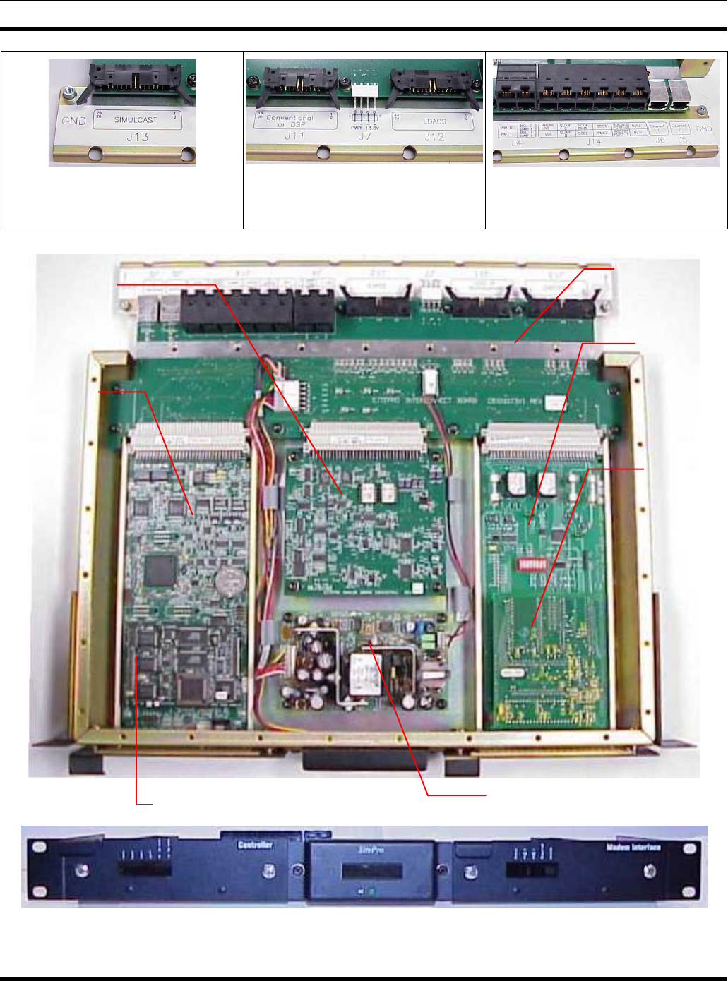
Figure 2 - SitePro Controller Shelf Assembly
DC/DC Power Supply (A5)
SitePro Modem Board (A2-A1)
Interconnect
Board (A1)
Rockwell
Modem
Interface
Card (A3)
Rockwell
Modem
Controller
Board (A2)
Analog
Board (A4)

CIRCUIT ANALYSIS
24 MM101271V1 R2A
7.0 CIRCUIT ANALYSIS
The Theory of operation of each circuit board/card and module used in SitePro Controller
Shelf Assembly EA101209V1 is described in the following paragraphs. Refer to the
Block Diagram in Figures 3 and 4 and Outline and Schematic Diagrams as listed in the
TABLE OF CONTENTS.
The SitePro Controller is a Base Station Controller with redundant communication links
[Backup Serial Links (BSL’s)]. The BSL’s provide for inter-channel communication.
Two 10Mbit Ethernet Ports provide system level communication. The BSL’s provide
trunking communications as well as site configuration and database messaging. One
Ethernet port is dedicated to Management System information. The second Ethernet Port
is not supported at this time.
The SitePro Controller and System Interface Module (SIM) will use the primary BSL for
trunking information and limited management system information. The secondary link
will ensure continued trunking operation in the event of a primary BSL failure.
The SitePro Controller/base station interface for digital information, both receive and
transmit, is 9.6k baud synchronous data. Additional digital control information is
provided via discrete I/O at both the base station and controller. The following diagram
(Figure 2) is a high level picture of the SitePro Controller and external interfaces.
7.1 SHELF ASSEMBLY
SitePro Controller shelf Assembly EA101209V1 is a 19” Rack Mount, one Rack Unit
device. It is enclosed to reduce emissions and interference with other devices. Serial
ports, Ethernet, power, and I/O connections are accessible at the back of the shelf (Figure
1). The serial port connections (6 OVER 6 PHONE LINES & SERIAL PORTS) are
stacked two high using RJ45 type connectors (J14) and RJ11 type connectors (J4). The
Ethernet connectors J5 & J6 (ETHERNET 0 & ETHERNET 1) are single height RJ45
connectors. The power connector (J7) and I/O connectors (J11, J12 & J13) are Molex
type.
The front panel has two hinged access doors for insertion/removal of the Controller
Board and the Rockwell Modem card for troubleshooting and ease of maintenance. These
doors have RF fingers to reduce emissions. Diagnostic LEDs and the eight-character
display are viewable from the front panel.
The Shelf Assembly consists of Interconnect Board A1, which provides connectors to
accommodate:
• Controller Board CB101069V1 (A2)
• Rockwell Modem Interface Card Assembly ROA 117 2247 (A3)
• Analog Board CB101070V1 (A4)
• Power Supply PS101328V1 (A5)
• Display Module MA101082V1 (A6)
CIRCUIT ANALYSIS
MM101271V1 R2A 25
Loc PTT
Rem PTT
A/D ModCtrl
HSD
LSD
PA Fail
Local Rx Audio
Local Tx Audio
RUS
Rem Audio Flag
Local Rx Mute
Synth_Locked
Synth_Clk
Synth_Data
Synth_LdEn
ADCin
bypass
inhibit
ext_PTT
ext_ADModCTrl
ext_150
ext_HSD
TxClk_in
TxClk_alarm
E0
E1
SCC1
SCC2
SCC3
SMC1
BSL/FSL0
BSL/FSL1
Com3
Com4
SP0
SP1
Controller
Analog
Power Supply
(switch mode)
SSP0
SSP1
SSP2
External (simulcast)
Signals and Control
Conventional
Signals and Control
Local (station)
Signals and Control
Voter
Signals and Control
Local (RF) HSD
SitePro Interface
FILTERS
LINE DRIVERS
ANALOG SWITCHES
ADC
MPC860
DS80C323
QUART
USRT
PLD
+5v @2a
+/- 12v
EtherNet Ports
Asynchronous
Serial Ports
RMIC
ROCKWELL MODEM
LINE DRIVERS
ANALOG SWITCHES
Voted (VDI) HSD
Remote (PL) HSD
CPTT
TxCGDis
CGMon
Vot_emsq
Vot_rcvng
Figure 3 - SitePro Shelf Assembly Block Diagram

CIRCUIT ANALYSIS
26 MM101271V1 R2A
7.2 INTERCONNECT BOARD (A1)
Interconnect Board CB101073V1 is a passive printed circuit board that provides
interconnections between all internal components of the SitePro Controller shelf and
interfaces the SitePro Controller shelf with the outside world (Refer to Table 3 -
Interface Connections, and Interconnection, Outline and Schematic Diagrams). Pi
filters U1 thru U29 reduce any Electro Mechanical Interference (EMI).
7.3 CONTROLLER BOARD (A2)
Controller Board CB101069V1 contains all SitePro Controller logic and control functions
except the power supply and Rockwell Modem (Refer to the Outline and Schematic
Diagrams for the Controller Board as listed in the TABLE OF CONTENTS).
This Controller Board is based on an MPC860 microprocessor, the primary responsibility
being message processing. This board has multiple high-speed serial ports, two of, which
are used for primary and secondary BSL’s. It has hardware and dual port RAM to support
the SitePro Modem Board and a 10/100 Mbit ethernet port. This port is available for
Voice Over IP traffic. A second 10 Mbit ethernet port is available for management
functions.
This board has sufficient memory to support 1M LIDs and 64k GIDs. It has LID and GID
validation for all calls.
7.3.1 Block Diagram
Figure 4 - Controller Board Block Diagram shows the connection of major components
from a high level viewpoint. Schematic Diagram WD-CB101069V1, Sheet 2 also
provides a Block Diagram for the Controller Board. These diagrams show the major
components of this board as:
• CPU (MPC860P)
• Ethernet 10 Base T
• Ethernet 10/100 Base T
• EEPROM
• Modem Board
• Memory:
⇒ FLASH
⇒ DRAM
• Electronically Programmable Logic
Device (EPLD)
• Quad UART (QUART)
• LEDS
• DIPSWITCH
• I2C Real-Time-Clock (RTC)
• Serial Ports
• Regulator
• Hot Swap Controller (HSC)
• Interconnect Board (Backplane)
7.3.2 System I/O
The System I/O circuits for the Controller Board are shown on Schematic Diagram WD-
CB101069V1, Sheet 3 and include:
• Oscillator For PHYs • 3.3V Power Monitor
• JTAG Port • Test Points
• Board Insert Detection Circuit • Programming Serial Port J8
• Hot Swap Controller • Decouplers
• 3.3V Regulator
CIRCUIT ANALYSIS
MM101271V1 R2A 27
MPC860P
59 MHz
MII
Enet PHY
10/100 BaseT
1:1 1:1
SDRAM
8M x 32
FLASH
1M x 32
I2C
EEPROM
32K x 8
32.768
kHz
RTC
29.4912
MHz
SMC1
SMC2
SCC4
BDM
QUART
RS-232
RS-232
EPLD RS-232
I/O Backplane
1
2
3
4
RS-232
RS-232
SitePro Modem Board
OUTs
INs
32
32
32
8
JTAG
INTsDATA
REG
5V
3.3V
PL
JTAG
JTAG
I/O
+12V
Enet PHY
10 BaseT
1:1 1:1
SCC1
LEDs
VDIRF
RS-232
RS-232
DIP SW
RS-232SCC2
RS-232
SCC3
I/O
Serial
Number
RS-485
BSL
BSL
XCVR
JTAG
5V
HSC
JTAG
I2C RTC
3.0V
Batt
32.768
kHz
DIAGNOSITC
PORT
Figure 4 - Controller Board Block Diagram

CIRCUIT ANALYSIS
28 MM101271V1 R2A
7.3.2.1 Oscillator For Ethernet PHYs
This circuit consists of crystal oscillator circuit Y1 powered by 3.3 V applied to Y1, Pin
4, Vcc. Oscillator circuit Y1 is biased on by resistor R49 connected to Y1, Pin 3, CTRL
and produces 25 MHz on the output at Pin 3 through resistor R51 (OSC 25MHz). This
output connects to the CLK25 inputs to the Ethernet 10 and Ethernet 10/100 Mbit
PHYs3.
7.3.2.2 JTAG Port
This JTAG PORT circuit consists of buffer U1 (NC7SZ125M5). This circuit allows
programming directly to the microprocessor through connector J4. This circuitry is not
presently used.
7.3.2.3 Board Insert Detection Circuit
This circuit consists of NPN transistors Q6 and Q7. When the Controller Board is
inserted into a live Interconnect Board, the base circuits of these transistors are connected
to ground through connector J1B, Pins B1 and B32 at either end of J2. Connector J1B,
Pin B1 is MATE-DETECT-A and J1B, Pin B32 is MATE-DETECT-B. With the base of
both transistors at ground, they are held in the off state. This allows POWER ON to cycle
high if the output of U41 is high. The POWER ON voltage is applied to Pin 2 of Hot
SwapTM Controller U37. If the base of either transistor (Q6 or Q7) is not connected to
ground, POWER ON will not be applied to the HotSwap Controller. Therefore, if the
card is not seated properly, power will not turn ON.
7.3.2.4 Hot Swap™ Controller
Hot Swap™ controller (HSC) U37 allows Controller Board CB101069V1 to be safely
inserted in or removed from Interconnect Board CB101073V1 while voltage is applied.
Using external N-channel pass transistor Q5, the supply voltage to the Controller Board is
ramped up at a controlled rate. Hot Swap switch driver U37, Pin 6 controls the N-channel
gate. A programmable electronic circuit breaker detecting over current by sensing voltage
across 15 milliohm resistor R153 protects against shorts. The RESET output (U37, Pin 1)
is used to generate a system reset when the supply voltage falls below the voltage preset
by resistors R167 and R168. The POWER ON input to U37, Pin 2 is used to cycle the
Controller Board power. The 555 timer circuit (U40) is connected to the HSC chip so that
the HSC can be automatically reset in the case of a circuit breaker fault.
Because the Hot Swap Controller, U37, latches OFF if it senses an overload, a timer
circuit has been added to occasionally turn it back ON. If the overload still exists, it turns
off immediately but if the overload is not present, normal operation is restored. This
circuit is needed for unattended operation.
The 555 timer is powered any time 5V is applied to the board since it is connected ahead
of the Hot Swap Controller. As long as the HSC is ON, 5V is fed to inverter U42-2
through D34. The resulting low on U42-4 holds U40 at reset.
When the HSC turns power OFF, U42-4 goes high and the reset is removed. The timer
now free runs with about a 1.1 second cycle time. U40-3 is high for about 0.7 sec and low
3 PHY is an Industry Standard for “Physical Interface.”

CIRCUIT ANALYSIS
MM101271V1 R2A 29
for about 0.4 sec. U40-3 is inverted by U41. During the high part of the cycle, the
resulting low at U41-4 holds the HSC ON pin low keeping the HSC OFF.
When U40-3 switches low, U37-2, the HSC ON pin is allowed to go high through D35,
pulled up by resistor R157. The HSC turns ON, but if the fault is still present, it turns
OFF within 40µs and the cycle continues. If the fault is gone, the 555 is held reset and the
Controller Board resumes normal functioning.
Capacitor C119 and resistor R191 act as a slugging filter on the FB input to prevent fast
transients on the 5V from causing the HSC to generate a reset. Likewise, capacitor C118
and resistor R190 prevent large transients on the input 5V, i.e. when the RMIC is hot
swapped, from causing the HSC to generate a reset due to a transient on the ON pin.
7.3.2.5 3.3V Regulator
The controller board is provided with 5 Volts and ±12 Volts from the Interconnect Board.
Linear regulator U25 is used to provide 3.3 volts to be used by the majority of digital
logic on the Controller Board and the Board.
The Hot Swap Controller (HSC) is used to ramp up the 5V-power rail at a controlled
rate. This, in addition to other considerations, will allow the Controller Board to be hot
swappable. The 5V output from this circuit will also power the 3.3-Volt regulator, thus
causing the 3.3 V power rail to also ramp up at a controlled rate. As mentioned above, the
HSC has a built-in electronic circuit breaker.
7.3.2.6 3.3V Power Monitor
The 3.3V Power Monitor (U31) uses a precision temperature-compensated reference and
comparator circuit to monitor the status of the 3.3V supply. If a loss of power is detected
an internal power-fail signal forces reset to the active state, which is low. When the 3.3V
supply returns to a normal state, the reset signal is kept active for approximately 150 ms
to allow the power supply and microprocessor to stabilize. This 3.3V Power Monitor
circuit also monitors Reset Pushbutton S1 on the reset output, U31, Pin 1. If the reset is
pulled low, by pressing S1, a reset signal is generated upon release. The output of U31 is
held in reset output (low) for approximately 150 ms.
7.3.2.7 Test Points
Test Points TP1 thru TP10 are provided on the Controller Board as follows:
• TP1 thru TP3, TP7, TP8 and TP10 are ground connections
• TP4 is +12V
• TP5 is +3.3V
• TP6 is +5.0V
• TP9 is WALSHCLK
7.3.2.8 Programming Serial Port J8
This port (J8) is located at the front of the Controller Board just behind the hinged door.
It is provided so that a programmer can easily program the microprocessor from the front
of the SitePro Controller without removing it from the cabinet.

CIRCUIT ANALYSIS
30 MM101271V1 R2A
7.3.2.9 Decouplers
Decoupling capacitors (Decouplers) are used to eliminate high-speed transient noise in
high-speed digital circuits. There are many decoupling capacitors used on the Controller
Board. These capacitors are connected between a source and ground. For example, on
sheet 3 of Schematic Diagram WD-CB101069V1 there are two 3.3V decoupling
capacitors, C2 and C87.
7.3.3 Backplane
The Controller Board to Interconnect Board A1 (Backplane) connector circuits are shown
on Schematic Diagram WD-CB101069V1, Sheets 4-7 and include:
• Board Connections • I/O (1)
• Serial I/O • I/O (2)
7.3.3.1 Board Connections
Schematic Diagram WD-CB101069V1, Sheet 4 shows the single DIN96 connector, J7.
This 96-pin connector has three layers of pins, J7A, J7B and J7C. Each layer consists of
32 pins. J7B, Pins 1 and 32 are the MATE-DETECT-A and MATE DETECT-B
connections. These two connections are used with the Board Insertion Detection circuit.
Pins J7B; Pins 27 and 28 are the SCL and SDA connections. SCL and SDA make up the
I2C bus. CPU I/O SIGNAL PROTECTION DIODES D27, D29 connected to SCL and
SDA provide surge protection for the I2C bus.
7.3.3.2 Serial I/O
Numerous asynchronous and synchronous serial ports are brought to the Interconnect
Board (Backplane) from the microprocessor, Modem Board and QUART. Most serial
ports convert to standard RS-232 levels using RS-232 transceivers U13, U24, U30 &
U36. Serial port U21 converts to RS-485 differential signal levels and supports a
multidrop network. One microprocessor RS-232 port is used as a diagnostic or local
programming port and is brought to RJ-11 connector J8 on the front of the board. Two
ports from the QUART use BSL signaling.
All Serial ports are designed for full-duplex 115.2 kbaud communications with the
exception of the RS-485 port U21 from the microprocessor SCC. This port is a half-
duplex HDLC port and supports speeds up to 2 Mbaud.
U21 is a differential bus transceiver for bi-directional data communication on multiport
bus transmission lines. This device combines a 3-state differential line driver and a
differential input line receiver. The driver and receiver have active-high and active-low
enables that are connected together externally to function as a direction control. The
driver differential outputs and the receiver differential inputs are connected internally to
form differential input/output I/O bus ports. These ports are designed to offer minimum
loading to the bus when the driver is disabled or Vcc=0.
BSL signaling is accomplished through two identical circuits consisting of hex inverting
Schmitt Triggers U23A/U23B, inverter buffer drivers U35A/U35B, Field Effect
Transistors (FET) Q3/Q4, NPN transistors Q9/Q10 and diodes D23/D25. Inputs to the
microprocessor from the Interconnect Board (backplane) are through diode D23/D25 to
the input of U23A/U23B. Schmitt Trigger U23A/U23B provides a well-defined output
CIRCUIT ANALYSIS
MM101271V1 R2A 31
for an input to the base of NPN transistor Q9/Q10. Transistors Q9/Q10 are used to
convert the RX level from 5V to 3.3V. The output of Q9/Q10 (RXA/RXB) is applied at
3.3V to the microprocessor. When the input (BKP-BSL0/BSL1) is high, diode D23/D25
is reversed biased making the input to U23A/U23B high and the output on the collector
of Q9/Q10 also high. When the input is low, diode D23/D25 is forward biased and the
input to U23A/U23B is low. The output on the collector of Q9/Q10 is also low.
Outputs from the microprocessor to the backplane are through inverter buffer driver
U35A/U35B, and FET Q3/Q4. The output RXA/RXB from the QUART is applied to the
input of inverter circuit U35A/B35B. When this input to U35A/B35B is low, the output is
high. This causes Q3/Q4 to conduct. Diode D32/D33 is forwarded biased and the output
to BKP-BSL0/BSL1 is low. Diode D32/D33 prevents loading the BSL when power is
off. When the input to U35A/U35B is high Q3/Q4 does not conduct and the output to
BKP-BSL0/BSL1 is high. FET Q3/Q4 is powerful enough to drive 1k ohm loads on up to
25 parallel connected shelves.
7.3.3.3 I/O
Other I/O’s are shown on Schematic Diagram WD-CB101069V1, Sheets 6 and 7. Inputs
to the EPLD from the backplane consist of identical circuits for different inputs. These
circuits consist of inverter buffer driver circuits U18A thru F, Schmitt Triggers U22B
thru D and U23C thru F (Figure 5 - Input Circuits U18A thru F, U22B thru D and U23C
thru F). Identical circuits for different inputs also include inverter buffer driver circuits
U22A, E, F, U29D and U32B (Figure 6 - Input Circuits U22A, E, F, U29D and U32B).
Figure 5 shows inputs using 74HC14's with diode coupling. When the input from the
backplane goes low the diode is forwarded biased and the input to the inverter goes low.
This results in a sharp, well-defined output of the inverter going high. Outputs are:
• REM-AUDIO PRESENT (U18A) • EXTADIN (U22C)
• CAS (U18B) • EXT150IN (U22D)
• CGMON (U18C) • RCVING-FROM-AV (U23C)
• LSDIN (U18D) • SYNTH-LOCK DET (U23D)
• PAFAIL (U18E) • SIMULCAST-INHBIT (U23E)
• FSLIN (U18F) • BYPASS (U23F)
• EXTPTTIN (U22B)
EPLD
BACKPLANE
5.0V 5.0V
BAV99
Figure 5 - Input Circuits U18A thru F, U22B thru D and U23C thru F
In Figure 6 the Schmitt Trigger provides a sharp, well-defined input to the
microprocessor
CIRCUIT ANALYSIS
32 MM101271V1 R2A
EPLD BACKPLANE
5.0V 5.0V
Figure 6 - Input Circuits U22A, E, F, U29D and U32B
The FSL output from the EPLD to the backplane is connected through inverter circuit
U33A and FET Q2 (BKP-FSL).
The RX-MUTE output from the EPLD to the backplane is connected through Inverter
U33D and transistor circuit Q1 (BKP-RX_MUTE).
The EMSQTOAV output from the EPLD to the backplane is accomplished through
Inverter U35C and transistor circuit Q6 (BKP-EMSQTOAV).
Other outputs from the EPLD to the backplane are connected through identical circuits as
shown in Figures 7 & 8. Figure 7 shows circuits using Schmitt Triggers U29B, C, E, F
and U32A & C to provide sharp, well-defined outputs to the backplane and to provide 5V
levels (Inputs are generally 3.3V). These outputs are:
• BKP-WALSH1 (U29B) • BKP-RFTXDAT (U29F)
• BKP-WALSH2 (U29C) • BKP-RFTXCLK (U32A)
• BKP-A/DMODCTL (U29E) • BKP-LSDOUT (U32C)
EPLD BACKPLANE
5.0V
0-5V0-3.3V
Figure 7 - Output Circuits U29B, C, E & F, U33C, E & F and U34A thru F
Figure 8 shows circuits using open collector inverters circuits U33B, C, E, F, U34A, B,
C, D, E, F and U35C, D, E & F. These outputs are:
CIRCUIT ANALYSIS
MM101271V1 R2A 33
• BKP-SYNTH_DATA (U33B)
• BKP-SYNTH_DATA_CLK (U33C)
• BKP-RPTKEY (U33E)
• BKP-SPARE2 (U33F)
• BKP-CPTTOUT (U34A)
• BKP-SPARE1 (U34B)
• BKP-STNPTT (U34C)
• BKP-RPT_INH (U34D)
• BKP-TXCGDIS (U34E)
• BKP-HSACO (U34F)
• BKP-EMSOTCAV (U35C)
• BKP-TXC_MISSING_ALARM
(U35D)
• BKP-REM_RPT (U35E)
• BKP-SYNTH_LD_EN (U35F)
EPLD BACKPLANE
5.0V
Figure 8 - Output Circuits U33B, C, E, F, U34A, B, C, D, E, F
and U35C, D, E & F
CIRCUIT ANALYSIS
34 MM101271V1 R2A
7.3.4 CPU
The Central Processing Unit (CPU) circuits, for the Controller Board, are shown on
Schematic Diagram WD-CB101069V1, Sheets 8 & 9 and include:
• Microprocessor • Microprocessor Support
7.3.4.1 Microprocessor
Microprocessor U94 is an MPC860P processor that has four SCC channels, two SMC
channels, plus a 100 Mbit Fast Ethernet Controller. One of the SCC channels is used as a
second ethernet port (10 Mbit) with all other SCC and SMC channels used as serial ports.
This microprocessor runs at 59 MHz using a 29.4912 MHz clock input. This frequency
was selected for use by the baud rate generators to produce standard baud rates up to
115.2 kbaud without error. The microprocessor external bus runs at half the speed of the
microprocessor (29.5 MHz).
The microprocessor provides an internal real-time clock that is used to provide time-of-
day information to the application software. The real time clock runs off of a 32.768 kHz
crystal. An external real-time clock is connected to the microprocessor through the 12C
bus. The microprocessor accesses the internal real-time clock much faster than the
external one. Therefore, whenever the board powers up, the battery-backed external real-
time clock is used to set the time of the internal real-time clock. Once the internal real-
time clock is set, it will always be used while the board is powered.
Four external interrupts are used in this design. The remaining unused three connect to
the EPLD for future use. Connecting them to the EPLD makes later modifications easier.
The external interrupt signals are specified in the following table.
Table 4 - External Processor Interrupt Signals
DEVICE IRQ
(SPARE-EPLD) IRQ (NMI)
QUART IRQ1
MODEM DB DUAL-PORT RAM IRQ2
(SPARE-EPLD) IRQ3
ETHERNET 10/100 IRQ4
ETHERNET 10 IRQ5
(SPARE-EPLD) IRQ6
All but one chip select are used in this design. The unused chip select is connected to the
EPLD for future use. The microprocessor chip select signals are defined in the following
table.
4 Microprocessor U9A and U9B are two parts of the same processor. This was done for drawing convenience.
CIRCUIT ANALYSIS
MM101271V1 R2A 35
Table 5 - External Chip Select Signals
DEVICE IRQ MACHINE DATA BUS WIDTH
FLASH CS0 GPCM 32 Bit
SDRAM CS1 UPMA 32 Bit
QUART REGISTERS CS2 GPCM 8 Bit
QUART INTERRUPT VECTOR CS3 GPCM 8 Bits
EPLD CS4 GPCM 8 Bits
MODEM DUAL PORT RAM CS5 UPMB58 Bits
MODEM CODE RAM CS6 GPCM 8 Bits
(SPARE-EPLD) CS7 N/A N/A
Note that there is both a 32-bit data bus and an 8-bit data bus. The 8-bit data bus is
connected to the 32-bit processor data bus via an 8-bit transceiver. The output enable for
the transceiver is controlled by ANDing all 8-bit chip selects together inside the EPLD.
7.3.4.2 Microprocessor Support
The microprocessor support as shown on Schematic Diagram WP-CB101069V1, Sheet 9
includes:
• BDM Debug Port Connector • Silicon Serial Number
• Power-On Reset Configuration • KAPWR Switch
• 32 kHz Crystal • 8-Bit Bus Transceiver
• VDDSYN Filter • MICTOR Logic Analyzer Connectors
BDM Debug Port Connector
For debug and development, microprocessor U9A provides a dedicated serial port (BDM)
for connecting a debugger/emulator. A debugger/emulator connected to this port allows a
programmer to read/write registers and external peripherals, control program execution,
etc. Many debuggers also have built-in capability to program on-board flash through this
port. These serial port pins are brought to 10-pin header J1 using the standard BDM
pinout.
Power-ON Reset Configuration
The Power-On Reset Configuration consists of four octal buffer/drivers U6A, U6B, U8A
and U8B with 3-state outputs. This circuit ensures that at Power-On all circuits are reset
to the starting state. Inputs to these circuits are through 10K BUS8 resistor networks RN7
and RN10. The outputs tie into bus D[0.31]. Each package is organized as two 4-bit line
drivers with separate output-enable (OE) inputs. These inputs are tied together and
connect to RESET-N. When RESET-N is low, data passes from A inputs to Y outputs.
When RESET-N is high, the outputs are in the high-impedance state. This circuit imposes
5 UPMB is only required if the system makes use of the BUSY_N signal coming from the dual port memory. If BUSY_N is
not used, then a GPCM machine can be used for this chip select.

CIRCUIT ANALYSIS
36 MM101271V1 R2A
predetermined "start-up" information on the microprocessor data bus during RESET. The
microprocessor reads the data bus state just before RESET goes inactive (high) and uses
the result for start-up initialization.
At power up, the MPC860 samples the data bus and the MODCK bits to obtain the
Hardware Configuration Word and clock setup parameters respectively. The SitePro
hardware configures these as follows:
Data bus 0x017A 0000
MODCK1, 2 1,0
This results in the following configuration:
Internal arbitration
Interrupt vector location 0xFFF0 0000
Boot Port size is 32 bits.
IMMR is at 0xFF00_0000.
Debug Pin Configuration is as follows: VFLS[01], VF0, VF1, STS, AT1, AT2, AT0,
AT3, OP3.
Debug Port Pin Configuration is DSCK, DSD1, DSD0, PTR1, TCK, TD1 and TD0.
External Bus speed set to ½ system clock.
Pitrtc connected to extclk and div by 4, pitclk = 32.768/4 = 8192 Hz
Sys clk connected to EXTCLK vco factor is 1, sysclk = 29.4912 MHz
32 kHz Crystal
This crystal circuit consists of crystal package Y3, resistors R90 and R98, capacitors C49
and C63. This circuits connects to microprocessor U9A between pins N1 (EXTAL) and
P1 (XTAL) and produces an oscillator frequency of 32.768kHz to drive the real-time
clock.
29 MHz Clock
The 29 MHz Clock consists of oscillator circuit Y2 and resistors R82 and R105. This
circuit produces the oscillator frequency of 29.4912 MHz and connects to microprocessor
U9A at N2 (EXTCLK).
VDDSYN Filter
This circuit consists of inductor L1 and capacitors C50 and C57. It filters the 3.3V supply
to the system Phase-Locked-Loop (PLL) circuitry on microprocessor U9A. The PLL
multiplies the EXTCLK by an integer factor to provide a bus clock.
Silicon Serial Number
A unique 64-bit electronic Serial Number chip U3 is used to store the board identification
number. This chip has a 1-bit serial port, which interfaces to microprocessor U9 through
an I/O port. In addition, four bits of hardware identification are made available to U9
through I/O ports. The Hardware ID is changed by selectively populating a bank of
resistors.

CIRCUIT ANALYSIS
MM101271V1 R2A 37
Real Time Clock (RTC)
A battery backed up Real Time Clock, U43, is provided to retain the elapsed time even
with power off. U43 can be read or written via the I2C bus. The slave address for U43 is
D0 hex. Accurate timing is maintained by 32.768kHz crystal Y5.
Processor U9 has an internal real time clock, however it consumes too much power to
allow battery back up. Therefore the real time is read from U43 via the I2C bus at power
up and stored in the processors RTC. This is a fairly slow process. Afterward, the
processor can quickly determine the time by reading the internal RTC. Timing for the
processor RTC is provided by 32.768kHz crystal Y3.
KAPWR
The Keep-Alive-PoWeR (KAPWR) circuit consists of 0-ohm resistor R196 and is used
for the "real time" clock on the microprocessor (860). KAPWR is not powered when
power is off. This circuit applies 3.3V supply to U9B, Pin R1 (KAPWR).
8-Bit Bus Transceiver
This circuit consists of 8-Bit Bus Transceiver U19 and resistor network RN15. The 8-Bit
Bus connects to the microprocessor through 8-Bit Bus Transceiver U19. The output
enable OE for the transceiver is controlled by ANDing all 8-bit chip selects together
inside EPLD U27. This transceiver drives the data bus for all 8-bit devices.
MICTOR Logic Analyzer Connectors
These connections consist of J3, J5 and J6. These connectors are for software
development and are not present in production units.
7.3.5 SitePro Modem Board Connector
The SitePro Modem Board connector circuits for the Controller Board are shown on
Schematic Diagram WD-CB101069V1, Sheet 10 and include:
• QUICC Connector (J9) • I/O Connector (J2)
7.3.5.1 QUIC Connector (J9)
The QUICC (J9) connector contains the microprocessor interface (Refer to the Modem
Board Section).
7.3.5.2 I/O Connector (J2)
The I/O (J2) connector has miscellaneous I/O to/from the EPLD or Interconnect Board
(Refer to the Modem Board Section).
7.3.6 Electrically Programmable Logic Device (EPLD)
The EPLD circuit for the Controller Board is shown on Schematic Diagram WD-
CB101069V1, Sheet 11. Also, refer to the EPLD Drawings listed in the Table of
Contents.
CIRCUIT ANALYSIS
38 MM101271V1 R2A
Access to various board inputs/outputs is made available through Electronically
Programmable Logic Device (EPLD) U27. The EPLD contains numerous read/write
latches with a simple 8-bit interface to the microprocessor.
The EPLD is in-circuit programmable via the JTAG port using an Altera Byte-blaster
cable. A 10-Pin header J10 is made available for this purpose. The EPLD JTAG port is
also brought to microprocessor I/O pins to allow the microprocessor to load the EPLD
configuration.
The JTAG port is routed to Modem board (A2-A1). This allows a future modem board to
be designed with an Altera EPLD. If that future EPLD modem board is used, resistor
R187 (0 ohms) must be removed from the board.
In addition to being an interface to the discrete I/O, the EPLD also divides clocks and
provides the output enable logic for the 8-bit data bus transceiver. It also derives the FSL
pulse stream from RFTXDAT and RFTXCLK in the Control Channel mode.
7.3.7 Ethernet Ports
There are two Ethernet Port circuits for the Controller Board shown on Schematic
Diagram WD-CB101069V1, Sheets 12 & 13 as:
• 10 Base-T (10 Mbit PHY) • 10/100 Base-T (10/100 Mbit PHY)
The 10/100 Mbit port (10/100 Base-T Transceiver U5) uses the Fast Ethernet Controller
(FEC) inside the microprocessor and supports full duplex (10/100 Base-T). The 10 Mbit
port (10 Base-T Transceiver U12) uses SCC1 and only supports half-duplex (10 Base-T).
The ethernet physical layer transceivers are the same for both ports, but the 10/100 Mbit
port uses a Media Independent Interface (MII), whereas the 10 Mbit uses a “7-wire”
interface. The ethernet transceivers support 10/100 Base-T with full auto-negotiation
capability, while the 10 Mbit port only advertises 10 Mbit capability.
The RJ-45 ethernet connectors are actually located on Interconnect Board A1. The
ethernet physical layer chips and transformers reside on the Controller Board with the
ethernet differential RX/TX signals brought to the RJ-45 connectors through the
Interconnect Board connector. A single LINK OK status LED is provided for each
ethernet port on the front of the Controller Board.
The 10Mbit Ethernet port uses the “7-wire” interface to connect the Ethernet physical
transceiver to the microprocessor SCC1 serial channel. When SCC1 is in Ethernet mode,
the SCC pins have different functions (refer to the following table).
Table 6 - 10 Mbit Ethernet Connections
SCC ETHERNET SIGNAL SCC PIN NAME PHY SIGNAL
TX TXD1 10TXD
TENA RTS1 10TXEN
TCLK CLKx 10TXCLK
CLSN CTS1 10COL
RENA CD1 10CRS
RX RXD1 10RXD
TCLK CLKx 10RXCLK
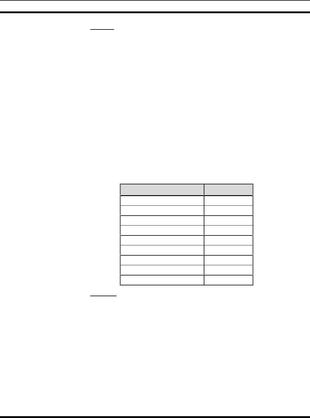
CIRCUIT ANALYSIS
MM101271V1 R2A 39
7.3.8 I2C Bus
The I2C-bus is a two-wire serial bus (SCL and SDA) used for microcontroller-based
control. The I2C Bus circuits, for the Controller Board, are shown on Schematic Diagram
WD-CB101069V1, Sheet 14. These circuits consist of Personality EEPROM U14 and 8-
bit I/O expanders for the I2C bus U15 and U26.
EEPROM U14 provides 16k of non-volatile data storage. EEPROM U14 is organized as
16kx8 and is accessible via the I2C port of microprocessor U9.
Serial EEPROM U14 has a write protect pin. It is active high and has an external pull-up.
To write to U14, port PB23 on the microprocessor is defined as an output and driven low.
To write protect the EEPROM after writing to it, port PB23 is defined as an input and the
pull-up activates the write protect signal.
Several peripherals are available to the microprocessor through the I2C Bus. In addition
to a 16kbyte EEPROM, there is an 8-bit writable latch for driving 4 LEDs and an 8-bit
readable latch for reading the status of an 8-bit DIP switch. The I2C bus is also brought to
the Interconnect Board for accessing other off-board peripherals (i.e. LED display). I2C
bus addresses are as follows:
Table 7 - I2C Bus Addresses
DEVICE ADDRESSES
LEDs 0x40
DIP Switch 0x46
EEPROM (Controller Board) 0xA0
Digital Pot 0x50
ADC/DAC 0x9E
16-Bit Expander 0x4C
Display 0x4A
Real-Time Clock 0xD0
EEPROM (Analog Board) 0xA6
7.3.9 Memory
The Memory circuits, for the Controller Board, are shown on Schematic Diagram WD-
CB101069V1, Sheets 15 & 16 and include:
• DRAM Circuits U2 & U7 • Flash Circuits U10 & U11
7.3.9.1 DRAM
Two 128-Mbit, 16 bit wide synchronous DRAM Integrated Circuits U2 and U7 are
organized in a 4M x 32 configuration. These two chips provide a minimum of 16 Mbytes
of storage, upgradeable to 64 Mbytes. The following table shows the MPC860P bank
addresses for the different DRAM memory sizes.

CIRCUIT ANALYSIS
40 MM101271V1 R2A
Table 8 - DRAM Bank Memory Ranges
BANK 64-MBIT (DRAM) 128-MBIT (2XDRAM) 256-MBIT (SDRAM)
Bank 1 0x003FFFFF – 0x00000000 0x003FFFFF – 0x00000000
0x013FFFFF – 0x01000000
0x003FFFFF – 0x00000000
0x013FFFFF – 0x01000000
0x023FFFFF – 0x02000000
0x033FFFFF – 0x03000000
Bank 2 0x007FFFFF – 0x00400000 0x007FFFFF – 0x00400000
0x017FFFFF – 0x01400000
0x007FFFFF – 0x00400000
0x017FFFFF – 0x01400000
0x027FFFFF – 0x02400000
0x037FFFFF – 0x03400000
Bank 3 0x00BFFFFF – 0x00800000 0x00BFFFFF – 0x00800000
0x01BFFFFF – 0x01800000
0x00BFFFFF – 0x00800000
0x01BFFFFF – 0x01800000
0x02BFFFFF – 0x02800000
0x03BFFFFF – 0x03800000
Bank 4 0x00FFFFFF – 0x00C00000 0x00FFFFFF – 0x00C00000
0x01FFFFFF – 0x01C00000
0x00FFFFFF – 0x00C00000
0x01FFFFFF – 0x01C00000
0x02FFFFFF – 0x02C00000
0x03FFFFFF – 0x03C00000
7.3.9.2 FLASH
Two flash memory chips U10 and U11 are organized as 1M x 32 for non-volatile
program storage (Flash). These two chips have 4 Mbytes of flash memory with the
ability of expansion up to 8 Mbytes. One or more flash sectors contain "bootloader" code,
which contains enough functionality to load and store new versions of application code.
7.3.9.3 Quad UART
The QUART circuit for the Controller Board is shown on Schematic Diagram WD-
CB101069V1, Sheet 17.
Quad Universal Asynchronous Receiver-Transmitter (QUART) U28 is used to handle
asynchronous serial data communication.
The serial port is a general-purpose interface that conforms to the Recommended
Standard–232C (RS-232C) and can be used to interface with almost any type of device
(modem, mouse and serial printer, etc.).
Quad UART U28 provides four additional serial ports for microprocessor U9. U28 is
powered by 3.3V, which forces the microprocessor interface to be asynchronous and run
at 14.75 MHz, the microprocessor bus clock divided by 2 inside the EPLD. The
communication clock input is 3.6864 MHz, the microprocessor bus clock divided by 8
inside the EPDL. None of the I/O ports of the QUART are used at this time.
The QUART uses two chip selects, CS2 and CS3. Chip select CS2 is used when
accessing the QUART registers. Chip select CS3 is used after an interrupt to read the
interrupt vector.

CIRCUIT ANALYSIS
MM101271V1 R2A 41
7.4 SitePro MODEM BOARD
The SitePro Modem Board contains three synchronous serial ports (modems) and a local
microprocessor. This board plugs into the Controller Board using two connectors,
QUICC (J9) and I/O (J2). Refer to Figure 9 - Site Pro Modem Board Block Diagram.
The microprocessor interface is a simple 8-bit bus port with two separate chip selects.
One chip select controls access to an 8k x 8 dual port RAM. The other chip select
controls access to the Modem Board microprocessor local code memory. The Controller
Board microprocessor loads the Modem Board local code memory with code before
releasing the Modem Board reset. The Modem Board microprocessor runs from a 14.7
MHz clock generated by dividing down the 29.5 MHz Controller Board microprocessor
output clock inside the EPLD.
Circuits for the SitePro Modem Board, are shown on Schematic Diagram WD-
CB101074V1, Sheet 1. The Outline Diagram is shown on AD-CB101074V1.
Modem Board CB101074V1 mounts on the Controller Board and exists primarily to
support Modem chips, U9, U10, and U11. These modems process 9600 baud serial
synchronous receive and transmit data from the RF path (U9), the Phone Line (PL) path
(U10) and the Voted Digital Interconnect (VDI) path (U11).
Microprocessor U1, a Dallas 80C323, controls the three modem chips, generates transmit
data, and processes receive data for use by the system.
The microprocessor communicates with the QUICC processor on the Controller Board
via Dual Port RAM U3.
There is no non-volatile memory on the Modem Board. Code is loaded into Code RAM
(U2) via an interface from the QUICC processor.
The microprocessor circuitry on the Modem Board operates from a 3.3V supply. The
Modem chips, however, require 5V. Thus a 3.3V to 5V conversion (U6) is needed for all
signals to the Modem chips.
7.4.1 Modems
Each Modem chip interfaces to the 80C323 microprocessor via an 8-bit bi-directional
address/data bus, and Chip Select (CS/), Read (RD/), Write (WR/), ALE, and Interrupt
(INT/) signals.
During transmit the microprocessor writes data to the Modem as requested by the Modem
interrupt. The Modem converts the data to a 9600-baud synchronous serial data stream.
During receive the Modem chip receives the 9600-baud synchronous serial data stream
and interrupts the 80C323 microprocessor whenever it has a complete byte to transfer.
The modem must also acquire bit sync and word sync from the data stream.
7.4.2 3.3V/5V Interface
Because the Modems require a 5V supply, and the microprocessor is on a 3.3V supply, it
is necessary to convert the voltage of signals passing between them. This is done by U6,
an IDT74FCT164245 3.3V/5V converter. Both output enable and direction can be
controlled for the two 8-bit sections of this IC.
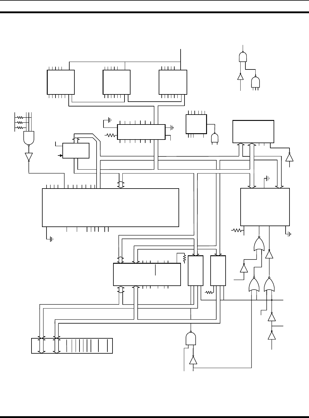
CIRCUIT ANALYSIS
42 MM101271V1 R2A
QD0 - QD7
QA0 - QA15
D0 - D7
A0 - A12
QUICC
IFC
J1 U3
DUAL
PORT RAM
U1
80C323
A0 - A7
A8 - A15
U7
8-BIT
LATCH
A0 - A15
D0 - D7
U2
CODE
SRAM
128k x 8
A0 - A15 A0
A14
D0
D7
U4
SRAM
128k x 8
U6
CONV
U9
RF
MODEM
U10
PL
MODEM
U11
VDI
MODEM
U13
DATA
BUFFER (8)
U12
ADDRESS
BUFFER (16)
A0 - A15
AD0 - AD7
A0 - A7
VDIMODCS/
U5
ADDRESS
DECODER
2
1
0
E
5
4
3
2
1
0
A15
A14
A13
DPRCS/
PLMODCS/
RFMODCS/
RD/
WR/
X1
X1
X1
A/D0-7
A/D0-7
A/D0-7
RFRXDAT
RFTXDAT
RFTXCLK
RFRCVDAT
RFRCVCLK
RFCS_5
ALE_5 CS/
ALE
RD_5
WR_5
RESET_5
RFINT
RD/
WR/
RESIN
INT/
RFMODCS/
PLMODCS/
UDIMODCS/
DATADIR
RD/
RESET G1
DIR OE
RFCS_5
PLCS_5
VDICS_5
ALE_5
RD/_5
WR/_5
RESET_5
RFMODCS/
PLMODCS/
ALE
RD/
WR/
RESET
VDIMODCS/
DATADIR
OE
DIR
3.3V
LE
RESETALE
U5
3.3V
RFINT/
PLINT/
VDIINT/
RXD0
TXD0
RSD1
TXD1
INT0/
INT/R
RWINT/
PLINT/
RD/
WR/
ALE
PSEN/
EA
X114.746 MHz
RESET RESET
RESET/RESET
RESETIN/
R/WL/
PSEN/
OE
DIR
D0 - D7
3.3V
R/W/L
CODECS/
CODE-A16
CODECS/QCODECS/
QRD/ DEL/
QDPRCS/ CEL/
QWR/ R/W/L
MODINT2NUC INTL/
BSY/ BUSYL/
14.756MHz 14.756MHz
RESET2MOD RESETIN/
RD/OEL/ OEL OER
CEL/ CEL CER DFRCS/
R/WL/ R/WRR/WL WR/
BUSYL/
SEML SEMR
INTL/ INTL# INTR INT/R
BUSYR
3.3V
M/S
DIR
OE
OE/
3.3 V
CODE-A16
A16
A0 - A15
RD/ OE/
CS/
WE/
WR/
A15
P3.4
P3.5
P1.1
P1.4
P1.6
P1.0
P3.0
P3.1
P3.2
P3.3
P3.2 INT0/
P3.3 INT1/
P1.5 INT3/
P1.7 INT5/
P3.7
P3.6
11 MHz
CODE-A16
CS/
WR/
WAL1
WAL2
LSRX
WALCLK
HSACQCTL
MODFSL
Figure 9 - Site Pro Modem Board Block Diagram
CIRCUIT ANALYSIS
MM101271V1 R2A 43
In this case, the outputs are always enabled, so the OE/ pins are tied low. Section 1 is
used for signals which only go from the microprocessor to the Modems, so Pin 1 (1DIR)
is tied high. Section 2 is used for the bi-directional bus. Pin 24 (2DIR) is driven by logic
which sets the direction from microprocessor to Modems (high) most of the time. Only
during a read of one of the modems is the direction reversed (low).
7.4.3 Microprocessor
The 80C323 microprocessor is a 3.3V version of the Dallas Speedy micro, an 80C32
derivative. It operates on a 14.7462 MHz. clock, which is convenient for generating
standard baud rates. It interfaces with the Modems, Code RAM, Dual Port RAM, and
Data RAM via standard address and data busses.
The microprocessor has 2 asynchronous serial ports (TXD0/RXD0 and TXD1/RXD1)
which may be used in the SitePro Controller system for diagnostics. Both ports are
available on the rear of the SitePro Controller shelf.
Six bits of 80C323 microprocessor I/O are used in a SitePro Controller configuration.
WALCLK, WAL1, WAL2, and HSACQCTL are outputs, while LSRX and MODFSL are
inputs.
The microprocessor has only two level sensitive interrupts, INT0/ and INT1/. The first,
INT0/, is used for all Modem interrupts. The second, INT1/, is used for interrupts from
the Dual Port Ram.
Since it is still necessary to distinguish between the three Modem interrupts, RFINT/ and
PLINT/ are brought to I/O pins so the microprocessor can easily determine which
Modem is interrupting. i.e. If a Modem interrupt occurs, the microprocessor looks at the
two pins. If either or both are low, the corresponding interrupts are serviced. If neither is
low, the VDI interrupt is serviced.
The 80C323 (U1) uses standard Intel multiplexed address/data bussing. During the first
half of the bus cycle, U7 latches the lower 8 bits of address under the control of ALE.
Address decoder U5 generates the Chip Selects for the three modems and the Dual Port
RAM using signals RD/, WR/, A13, A14, and A15.
Table 9 - Memory Map
MEMORY MAP
Device Range Addressable Size
Code RAM 0-FFFF 64K Bytes
Dual Port RAM 0-1FFF 8K Bytes
Data RAM 8000-FFFF 32K Bytes
RF Modem 2000-2003 4 Bytes
PL Modem 4000-4003 4 Bytes
VDI Modem 6000-6003 4 Bytes
7.4.4 Code Memory
Code is stored in 128K byte RAM U2. The microprocessor can then access it via the
Address and Data bus using PSEN/.
Code is loaded into U2 from the QUICC microprocessor. During loading, the QUICC
holds the 80C323 reset with the RESETIN/ (low) signal. This is required so the 80C323

CIRCUIT ANALYSIS
44 MM101271V1 R2A
will not try to access U2 at the same time causing bus contentions. During loading, bus
transceivers U12 (address bus) and U13 (data bus) are turned on. They are held inactive
at all other times by the same RESETIN/ signal.
The QUICC controls Code memory access through signals RESETIN/, R/WL/,
CODECS/ and CODE_A16. While RESETIN/ is held low, the QUICC can write or read
U2. CODE_A16 can be used to control which 64K byte half of U2 is used. Thus, for
instance, Control Channel code could be stored in one half and working channel code in
the other. The switch is performed, while the 80C323 is held at reset, so it is entirely
transparent to the 80C323.
When RESETIN/ is high, the bus transceivers U12 and U13 are off and the 80C323
controls the bus.
7.4.5 Data Memory
Data is stored in 128K byte RAM U4, however, only 32K is used. Chip select is A15/,
thus the RAM is addressed in the upper half of memory space.
7.4.6 Dual Port Ram
Dual Port RAM U3, an IDT70V05 8K byte device, is the communication link between
QUICC and 80C323 during normal operation. Either microprocessor can read or write
any location in the RAM. Protocols must be established in software to avoid contention.
The QUICC can interrupt the 80C323 by writing to Address 1FFF. This causes interrupt
line INTR/ to go low. It is cleared by a read of the same address by the 80C323.
Likewise, the 80C323 can interrupt the QUICC by writing to address 1FFE, which causes
a QUICC interrupt on line INTL/.
The 80C323 accesses the DPR via its address and data busses using signals DPRCS/,
RD/, WR/, and INTl/.
The QUICC accesses the DPR via its address and data busses using corresponding
signals CEL/, R/WL/, OEL/, and INTL/.
7.4.7 Troubleshooting Aids
Several signals are available on diagnostic connector J3 for troubleshooting purposes.
Also probe points are provided for GND, 5V, and 3.3V.
7.5 ROCKWELL MODEM INTERFACE CARD (A3)
The SitePro Controller shelf uses Rockwell Modem Interface Card ROA 117 2247/1 and
Rockwell Modem Assembly, RYTUA 921 01/1. For a Description and Circuit Analysis
of this card refer to Maintenance Manual LBI-39152.
7.6 ANALOG BOARD (A4)
Analog Board CV101070V1 contains programmable high-speed filters, low speed encode
and low speed decode filters. This board includes Simulcast Interface hardware, which
eliminates the need for the older Simulcast Interface Board in Simulcast applications.
Refer to Figure 11 - Analog Board Block Diagram, Outline Diagram AD-CB101070V1
and Schematic Diagram WD-CB101070V1.
CIRCUIT ANALYSIS
MM101271V1 R2A 45
7.6.1 Quad ADC and Single DAC
AD/DA Converter U23 is an 8-bit CMOS data acquisition device with four analog inputs,
one analog output and a serial I2C-bus interface. Three address pins A0 (Pin 5), A1 (Pin
6) and A2 (Pin 7) can be used for programming a hardware address, allowing up to eight
similar devices to be connected to the I2C-bus without additional hardware. In this
application, these three leads are tied to +5V. Address, control and data to and from the
device are transferred serially through the two-line bi-directional I2C-Bus. The PWR
SENSE lead is connected to analog input AIN0 at U23, Pin 1, converted to a digital word
and read via the I2C-bus. Monitoring PWR SENSE is the only application for the AD
Converter at present.
The I2C address is 9E hex. Bits 7-4 are hardwired in the device. Bits 3, 2, 1 are A2, A1 &
A0. Bit 0 is the Read/Write bit.
R/W
A2
1
A1
1
A0
1
HARD
WIRED
PINS
1001
Figure 10 - I2C Address
7.6.2 8-Bit I/O Expander for I2C Bus
I/O Expander U4 is a 16-bit two-line quasi-bi-directional port and an I2C-bus interface.
The two-line I2C inputs SCL and SDA connect to U4, Pins 22 and 23 respectively. These
two-line inputs can be monitored at Test Points TP2 and TP3. The expanded outputs and
connections are U4,
• Pin 4 (P0) – HS-FILTERSEL0
(Monitored at TP19)
• Pin 13 (P10) - ground
• Pin 5 (P1) – HS-FILTERSEL1
(Monitored at TP24)
• Pin 14 (P11) - ground
• Pin 6 (P2) – HS-FILTERSEL2
(Monitored at TP25)
• Pin 15 (P12) - ground
• Pin 7 (P3) – HSACOCTL1 (Monitored
at TP26
• Pin 16 (P13) – ground
• Pin 8 (P4) – LSCTL (Monitored at
TP30)
• Pin 17 (P14) - ground
• Pin 9 (P5) - (Monitored at TP29)
Not Used
• Pin 18 (P15) – Pulled up to +5V
through resister network R127, Pin 8
• Pin 10 (P6) – MODCTL (Monitored at
TP28)
• Pin 19 (P16) – Pulled up to +5V
through resistor network R127, Pin 7
• Pin 11 (P7) – LSDATAACC
(Monitored at TP27)
• Pin 20 (P17) – Pulled up to +5V
through resistor network R127, Pin 5
CIRCUIT ANALYSIS
46 MM101271V1 R2A
7.6.3 –5 Volt Generation
-5 Volt generation is accomplished through voltage regulator U2. –12 Volts is applied to
U2, Pin 4 IN. Capacitors C3 and C4 provide filtering of this input. The output is at U2,
Pin 3 Out. The –5 Volts is filtered by capacitors C5 and C6. –5Volts can be monitored at
Test Point TP31.
7.6.4 High-Speed Data Transmit Filters
The High Speed Data Transmit Filter section consists of an input buffer, five selectable
High-Speed filters, an 8:1 MUX, a digital pot, output buffering and an analog switch.
Buffer/follower circuit U6A precedes the high-speed data transmit filter circuits for
RFTXDAT. The output of this circuit can be monitored at TP1. The output of U6A is
applied to the inputs of high-speed Data Transmit Filters:
• 9600 Baud Wide Band
• 4800 Baud Narrow Band
• 9600 Baud Wide Band ETSI6
• 4800 Baud Narrow Band ETSI
• 9600 Baud Narrow Band Switched Capacitor Filter Circuit
The High Speed Data (HSD) filter filters data transitions to minimize the high-speed-data
transmission bandwidth. The frequency response of the HSD filter section is changed by
selecting the output of only one filter circuit with 8:1 MUX U7.
High-speed data is a 4800 or 9600 bit per second data stream generated by the
microcomputer through the RF data modem U9 on the Modem Board.
7.6.4.1 9600 Baud Wide Band
This HSD filter circuit consists of operational amplifier U5B followed by operational
amplifier U5A. The output of U5A, Pin 1 is applied to the input of 8:1 MUX U7, Pin 4
(N01). This HSD amplifier filter output can be monitored at TP4.
Table 10 - 9600 Baud WB Filter Response
FREQUENCY RESPONSE
1000 Hz 0 dB (ref)
10 Hz 0 dB ± 1dB
3000 Hz 0 dB ± 1dB
6000 Hz -2 dB ± 1dB
7000 Hz -3 dB ± 1dB
20000 Hz <-20 dB
6 European Technical Standards Institute
CIRCUIT ANALYSIS
MM101271V1 R2A 47
7.6.4.2 4800 Baud Narrow Band
This HSD filter circuit consists of operational amplifier U5C followed by operational
amplifier U5D. The output of U5D, Pin 14 is applied to the input of 8:1 MUX U7, Pin 5
(N02). This HSD amplifier filter output can be monitored at TP5.
Table 11 - 4800 Baud NB Filter Response
FREQUENCY RESPONSE
500 Hz 0 dB (ref)
10 Hz 0 dB ± 1 dB
1500 Hz 0 dB ± 1dB
3000 Hz -2 dB ± 1dB
3500 Hz -3 dB ± 1dB
10000 Hz <-20 dB
7.6.4.3 9600 Baud Wide Band ETSI
This HSD filter circuit consists of operational amplifier U10B followed by operational
amplifier U10A. The output of U10A, Pin 1 is applied to the input of 8:1 MUX U7, Pin 6
(N03). This HSD amplifier filter output can be monitored at TP6.
Table 12 - 9600 Baud WB ETSI Filter Response
FREQUENCY RESPONSE
1000 Hz 0 dB (ref)
10 Hz 0 dB ± 1dB
2000 Hz 0 dB ± 1dB
3600 Hz -2 dB ± 1dB
4600 Hz -3dB ± 1dB
12000 Hz <-20 dB
7.6.4.4 4800 Baud Narrow Band ETSI
This HSD filter circuit consists of operational amplifier U510C followed by operational
amplifier U10D. The output of U10D, Pin 14 is applied to the input of 8:1 MUX U7, Pin
7 (N04). This HSD amplifier filter output can be monitored at TP7.
Table 13 - 4800 Baud NB ETSI Filter Response
FREQUENCY RESPONSE
500 Hz 0 dB (ref)
10 Hz 0 dB ± 1dB
1000 Hz 0 dB ± 1dB
2300 Hz -2 dB ± 1dB
3000 Hz -3 dB ± 1dB
8000 Hz <-20 dB
CIRCUIT ANALYSIS
48 MM101271V1 R2A
7.6.4.5 9600 Baud Narrow Band
This HSD filter circuit consists of switched-capacitor filter circuit U11 required to
produce a narrow frequency response. This circuit is driven by an external 400 kHz clock
on U11, Pin 1. The output on U11, Pin 5 is applied to the input of 8:1 MUX U7, Pin 12
(N05). This HSD filter circuit output can be monitored at TP8.
Table 14 - 9600 Baud NB Filter Response
FREQUENCY RESPONSE
100 Hz 0 dB (ref)
10 Hz 0 dB ± 1dB
3800 Hz <-3 dB
4400 Hz <-3 dB
11000 Hz <-20 dB
7.6.4.6 8:1 MUX
Multiplexer circuit U7 is used to select the applicable HSD to be passed on to Dual
Digital Potentiometer U8. The inputs to U7 are applied to N01 through N05 (Pins 4, 5, 6,
7 and 12). The selection of HSD is made by the HS-FILTER_SEL inputs on U7, Pin 1
(A0), Pin 16 (A1) and Pin 15 (A2).
Table 15 - HSD Selection
A2,A1,A0 ACTION NO# HSD
000 Selects NO1 9600 WB
001 Selects NO2 4800 NB
010 Selects NO3 9600 WB ETSI
011 Selects NO4 4800 NB ETSI
100 Selects NO5 9600 NB
101 6
110 7
111 8
Quiet
EN (Enable) on Pin 2 is connected to +5V always enabled. The 8:1 MUX output COM is
on U7, Pin 8. Selections of NO6 through NO8 (all grounded) results in a quiet output.
7.6.4.7 Dual Digital Pot
The output of the MUX circuit connects to the input of Addressable Dual Digital
Potentiometer U8, Pin 14 (HO). This device has two independently controlled
potentiometers. Only one pot is used in this application. The wiper can be set to one of
256 positions and is controlled by the microprocessor through the I2C data bus SCL (Pin
9) and SDA (Pin 10). The output on Pin 12 (WO) connects to the input of amplifier
circuit U6B. Pot I2C address is 50 hex.

CIRCUIT ANALYSIS
MM101271V1 R2A 49
7.6.4.8 Inverting Buffer/Amplifier
Amplifier circuit U6B is an inverting buffer/amplifier with a gain of approximately 1.5.
The output of this circuit is connected to the input of analog switch U9. The output of this
circuit can be monitored at TP9.
7.6.4.9 Analog Switch
Analog Switch U9 is a Single-Pole/Double Throw (SPDT) with one normally closed and
one normally open switch. Analog Switch U9 switches between RFTXDATA (U9, Pin 2
(S1)) coming from inverting Buffer/amplifier U6B and ANALOG AUDIO (U9, Pin 8
(S2)) under the control of MODCTL, Pin 6 output of I2C I/O Expander U4. S1, Pin 2
(RFTXDATA) is connected when MODCTL=0. The output is on U9, Pin 1 (D) MOD.
7.6.5 Clock Generation
Clock generation is accomplished by inverter circuits U32C and U32D and Dual 4-Stage
Binary Ripple Counter U3. U32C and 400 kHz crystal Y1 form a 400 kHz Pierce
oscillator circuit. The output of U32C connects to the input of buffer U32D. The 400 kHz
clock (CLK) output of 32D connects to U3, Pin 1 (CP1). This 400 kHz CLK can be
monitored at TP10. Counter U3 divides the 400 kHz CLK down to produce a 25 kHz
CLK. This output can be monitored at TP11. The 400 kHz CLK is further divided down
to produce a 3.125 kHz CLK. This output can be monitored at TP12.
7.6.6 Low -Speed Data Decode Filters and Slicer
The Low-Speed Data Decode Filter is used to remove voice-audio (300-3000 Hz) leaving
only the low-speed or subaudible data for an input to the microprocessor.
VOL/SQ/HI couples both high and low speed data through capacitor C33 to the input of
buffer/follower circuit U15A. The output of U15A, monitored at TP13, connects to the
input of two circuits. The first connection is the input to the low speed data decode filter
through operational amplifier U15B. The second connection is the input of a high-speed
data slicer circuit consisting of MUX U31 and voltage comparator U33A.
Low-Speed Decode Filter:
Operational amplifier U15B provides an approximate gain of 2:1, monitored at TP15.
The output of U15B connects to the input of high pass filter U16. High pass filter U16 is
driven by a 3.125 kHzCLK on Pin 16 (CLK) and is a 4th order Butterworth filter. It
provides -3 dB rolloff @ 50 Hz and -35 dB rolloff @ 18 Hz (Table 16 - Low Speed Data
Decode Filter Response). The output of U16, monitored at TP16, is applied to the input
of low pass filter U14. Low pass filter U14 is synchronized by a 25 kHz clock applied to
Pin 3 (CLK) and is an 8th order elliptic filter. It is flat to 250 Hz and provides more than -
40 dB rolloff @ 300 Hz.
The output of U14, monitored at TP17, is applied to the input of buffer/amplifier U28A
though 0 ohm resistors R61 and R61. U28A provides a gain of 2, monitored at TP18. The
output of U28A connects to the input of voltage comparator circuit U12B.
Analog switch U18 connects/disconnects resistor R67 normally in parallel with resistor
R60 connected to U12B, Pin 6. This function is controlled by LSDATAACQ on U18, Pin
6 (IN). LSDATAACQ is one of the I2C I/O expander outputs. When Pin 6 is low R67 is
CIRCUIT ANALYSIS
50 MM101271V1 R2A
in parallel with R60. When Pin 6 is high R67 has been removed from the circuit. Moving
R67 in and out of the circuit adjusts the input time constant to U12B, Pin 6.
Voltage comparator U12B provides a square wave output that swings from +12 to -12
volts, monitored at TP14. This output is applied through resistor R58 to the base of NPN
transistor Q1. Transistor Q1 interfaces the limited signal LSIN to the Controller Board.
Table 16 - Low Speed Data Decode Filter Response
FREQUENCY RESPONSE
100 Hz 0 dB (ref)
50 Hz -3 dB ± 1dB
18 Hz -35 dB ± 3 dB
250 Hz -0 dB ± 1dB
300 Hz <-40 dB
High Speed Slicer
The High Speed slicer circuit converts 9600 baud noisy received data to hard 1's and 0's,
producing a +5Volt square wave at the output of U33A. This output is controlled by the
HSACQCTL0 and HSACQCTL1 inputs to U31, Pins 1 (A0) and 14 (A1) respectively.
HSACQCTL0 is controlled directly by microprocessor 80C323 rapidly controlling the
receive acquisition rate by adjusting the input time constant to U33A. The Time Constant
(TC) is adjusted to provide a fast TC to follow the initial frequency variation of the
transmitting radio, then a slow TC to better slice the data after the frequency becomes
stable.
The TC is adjusted by selecting a resistor to connect in the negative input terminal of
U33A (Pin 2). Resistors are selected as shown in the following table:
Table 17 - Acquisition Rates
A1, A0 NO# RESISTOR ACQUISITION
00 NO1 R40 FAST
01 NO2 R43 SLOW
10 NO3 R125 ETSI FAST
11 NO4 R126 ETSI SLOW
A0 = HSACQCTL0
A1 = HSACQCTL1
HSACQCTL1 is controlled by the I2C bus and is only changed at power up or reset to
switch between US and ETSI bandwidths.
The output of the high-speed data decode filter RFRXDAT connects to the Controller
Board.
7.6.7 Low Speed Data Encode Filter
The Low Speed Data Encode filter is used to smooth out transitions of data impressed
upon the voice audio. Low-speed data is a 150 bit per second data stream generated by
the microcomputer and used to produce subaudible data on the voice audio.
CIRCUIT ANALYSIS
MM101271V1 R2A 51
Low-Speed Data is generated by microcomputer U1 on the Modem Board through EPLD
U27, Pins 81 and 80, Walsh Bit 1 and Walsh Bit 2 respectively. For low-speed data, the
two Walsh bits are scaled by resistors R91 and R95 and summed through analog switch
U22. The output of U22, Pin 1 (D) connects through operational amplifier U19A and
buffer/follower U19B to the input of the low-speed-data encode filter U20. Operational
amplifier U19A produces a loss of -9 dB at TP23. The output of buffer U19B, monitored
at TP22 connects to the input of low-pass filter U20, Pin 14 (IN). Low pass filter U20 is
synchronized by a 25 kHz clock applied to Pin 3 (CLK) and is an 8th order elliptic filter.
For the frequency response refer to the following table.
Table 18 - Low-Speed Data Encode Filter Response
FREQUENCY RESPONSE
100 Hz 0 dB (ref)
5 Hz +1 dB ± 2dB
150 Hz -1.5 dB ± 1 dB
250 Hz -4 dB ± 1dB
300 Hz <-40 dB
The output of this filter, monitored at TP21, connects through 0 ohm resistor R84 to the
input of operational amplifier U17A, Pin 3. U17A provides a gain of 2:1. LSDTX
connects to J1B, Pin 21 through Interconnect Board A1 to the EDACS connector J12, Pin
23 (LSDTXMOD). This provides the low frequency Channel Guard modulation input to
the base station transmitter.
7.6.8 Simulcast Control Circuits
Simulcast control circuits, consisting of RS-232 and RS-422 drivers, convert (RS-232 -
TTL - RS-422) and buffer control signals coming from SitePro Controller Board A2.
Refer to the second page of Figure 11 - Analog Board Block Diagram. These signals are
passed through Simulcast connector J13, on Interconnect Board A1, and connect to the
Simulcast cross connect panel. Likewise, RS-422 drivers convert (RS-422 to TTL) and
buffer signals coming from the cross connect panel, passing through A1 and going to
SitePro Controller Board A2.
A Simulcast "bypass" control signal, when low, forces the Simulcast site to operate in a
non-Simulcast mode and is driven by Simulcast control equipment. The active low
bypass control line, BYPASS, originates at the Simulcast control equipment, and is used
to re-route audio paths at the SitePro interface module located in a station interface panel.
It also serves to re-route 9600 BPS data, 150 BPS data, A/D control line and the PTT
control line, all of which are directed back to the SitePro Controller Board.
Control Signals
RS-232 Drivers/Receivers U24 and Quad RS-422 Line Driver U25 converts and buffers
signals coming from the SitePro Controller Board and going to the Simulcast cross
connect panel. These signals are:
• PLTXDAT (IN)
• PLTXCLK (IN)
• PLTXDAT + (OUT)
• PLTXDAT - (OUT)
• PLTXCLK + (OUT)
• PLTXCLK - (OUT)

CIRCUIT ANALYSIS
52 MM101271V1 R2A
Quad RS422 receiver U26 converts and buffers signals coming from the Simulcast cross
connect panel going to the SitePro controller Board. These signals are:
• 150 Hz + (IN)
• 150 Hz - (IN)
• 9.6 DATA + (IN)
• 9.6 DATA - (IN)
• 9.6 REF + (IN)
• 9.6 REF - (IN)
• EXT 150 Hz + (OUT)
• EXT 9.6 DATA + (OUT)
• EXT 9.6 REF + (OUT)
Audio Switching
The audio bypass circuit consisting of relay driver U27 and relays K1 and K2 allows the
audio to be interrupted and receive voice to be sent back to the station, when in the
bypass mode.
In normal Simulcast operation Rx AUDIO L connects through relay K1 to RXV R. TX
AUDIO L connects though K1 to TXV R. Also, RX AUDIO H connects through relay
K2 to RXV T. TX AUDIO H connects through K2 to TXV T.
When the BYPASS signal goes low, forward biasing diode D15, relay drivers U27 cause
relays K1 and K2 to activate. This action places the Simulcast System in the Bypass
mode. RX AUDIO L now connects through K1 to TX AUDIO L. Likewise, RX AUDIO
H connects through K2 to TX AUDIO H, returning the audio back to the station.
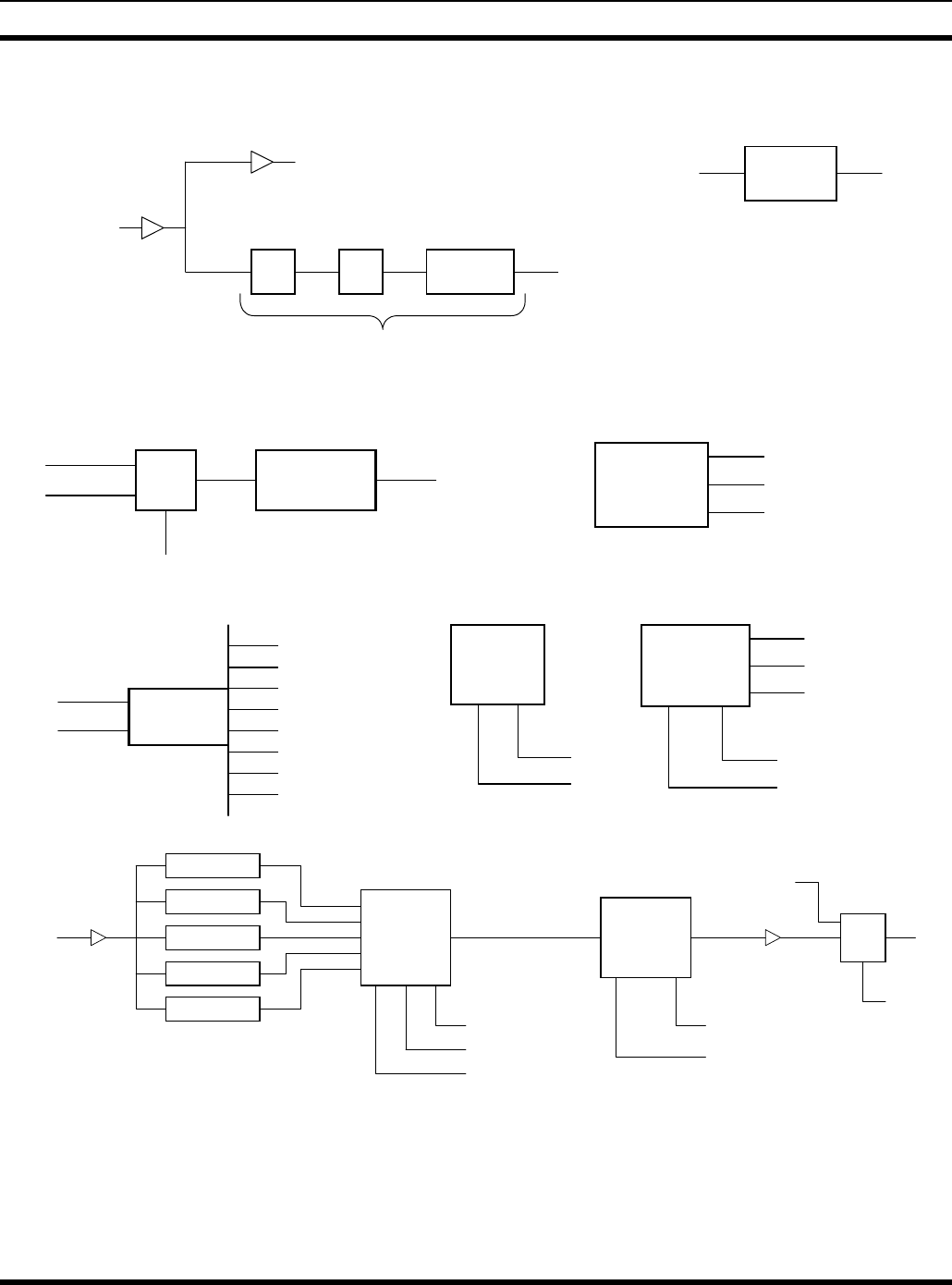
CIRCUIT ANALYSIS
MM101271V1 R2A 53
VOLSQHI
SLICER
RFRXDAT
LSIN
HIGH
PASS
LOW
PASS LIMITER
LS
DECODE
FILTER
-5 VOLT
REGULATOR
-12 V -5 V
MUX
LOW SPEED
ENCODE
FILTER
WALSH 1
LSDTX
150 Hz
LSCTL
CLOCK
(400 kHz
OSC)
400 kHz
25 kHz
3.125 kHz
SDA
SCL
I2C
EXPANDER
HS_FILTER_SEL 0
HS_FILTER_SEL 1
HS_FILTER_SEL 2
HSACQCTL 1
LSCTL
Bit 5 (Not Used)
MODCTL
LSDATAACQ
I2C
EEPROM
U34
SCL
SDA
SCL
SDA
I2C
ADC & DAC
SPARE D/A
SPARE A/D
PWR SENSE
RFTXDAT
9600 BAUD
WIDEBAND
4800 BAUD NARROW
BAND
9600 BAUD
WIDEBAND ETSI
4800 BAUD
NARROW BAND ETSI
9600 BAUD
NARROW BAND
MUX
HS_FILTER_SEL 0
HS_FILTER_SEL 1
HS_FILTER_SEL 2
I2C
DIGITAL POT
SDA
SCL
MUX MOD
MODCTL
ANALOG_AUDIO
Figure 11 - Analog Board Block Diagram
CIRCUIT ANALYSIS
54 MM101271V1 R2A
RS-232 RX
PLTXCLK PLTXCLK +
PLTXDAT +
PLTXDAT -
PLTXDAT
PLTXCLK -
RS-422 TX
RS-422 RX
150 Hz +
150 Hz -
9.6 DATA +
9.6 DATA -
9.6 REF +
9.6 REF -
EXT150HZ
EXT9.6DATA
EXT9.6REF
RX_AUDIO_H
RELAY
DRIVER
RELAYS
K1 & k2
TXV_R
RXV_R
RX_AUDIO_L
TX_AUDIO_L
TX_AUDIO_H
TXV_T
RXV_T
SIMULCAST INTERFACE CIRCUITS
BYPASS
Figure 11 - Analog Board Block Diagram (Continued)
CIRCUIT ANALYSIS
MM101271V1 R2A 55
7.7 POWER SUPPLY (A5) PS101328V1
The power supply used with the SitePro Controller is a 40 watt DC-DC, open frame
supply (Figure 2 - SitePro Controller Shelf Assembly). Specifications for this supply are:
INPUT VOLTAGE: 24 VDC nominal; 10-30 VDC continuous input.
INPUT CURRENT: Maximum input current at minimum 10 VDC
with full rated output load at 6 Amps max.
DC OUTPUTS:
OUTPUT OUTPUT
(V)
MINIMUM
LOAD
CURRENT (I) TOTAL
REGULATION
V1 OVP
SET.
RIPPLE
AND
NOISE
NOTES
1 +5.1 V 0.1 Amp 4 Amps 2% 6.2±0.6V 1%
2 +12 V 0.05 Amp 2 Amps 6% 1% A & B
3 -12 V 0 Amps 0.4 Amp 5% 1%
OUTPUT POWER: Normal continuous output power is 40 W, 45 W
peak for 60 seconds.
OVERLOAD PROTECTION: Fully protected against short circuit and output
overload.
TEMPERATURE RANGE: -30 to 60°C at full rated output power.
HUMIDITY: Operating 0-95% RH
ALTITUDE: Operating -500 to 10,000 ft.
7.8 MISCELLANEOUS INFORMATION
7.8.1 Serial Port Data Format
The serial ports transfer RS-232 asynchronous serial data at a rate of 38.4k using the half-
duplex operating mode. That is, data flows in only one direction at a time. The
characteristics of the communication link are:
Type: RS-232C
Baud Rate: 38.4 kilobaud
Start Bits: 1
Stop Bits: 1
Parity: None
Data Type: Binary
PERSONALITY PROGRAMMING
56 MM101271V1 R2A
8.0 PERSONALITY PROGRAMMING
A personality is a computer file generated by the user. This file (or personality) is
downloaded into the SitePro Controller and contains data that directs operating
characteristics of the SitePro Controller unit. This allows each SitePro Controller to be
programmed as required by the application. The SitePro Controller personality includes
system configuration information such as channel frequencies, call parameters, operating
modes, and identification information.
The personality programming process stores data in non-volatile regions of memory. The
SitePro Controller shelf has its personality stored in two locations. The first location is
EEPROM U14 on Controller Board A2 and contains general site level information. The
other location is EEPROM U34 on Analog Board A4 and contains general channel level
information. Programming is performed through serial programming port J8 on the front
of the Controller Board (Figure 13 - Location of Serial Programming Port J8).
Programming can also be accomplished through an Ethernet connection.
The Personality Programming process involves using SitePro PC Programmer TQ3408
software, which creates the desired personality and transfers the Personality data to the
EEPROM's U14 on the Controller Board and U34 on the Analog Board.
Equipment Required:
• Computer capable of running Windows95/98NT/2000/ME, which has a serial and/or
Ethernet port according to following tables.
• Programming Manual MM101461V1
• Programming software TQ3408
• Programming cable CA101302V1
• Male DB-25 to female DB-9 adapter or cable if the computer serial port is a male
DB-9 connector instead of a male DB-25 connector
Table 19 -Minimum Operating System Requirements
Windows 9x Windows NT Windows 2000
Processor Speed Pentium II 300
MHz
Pentium II 300
MHz
Pentium II 300
MHz
RAM for Windows 16 Megabytes 24 Megabytes 64 Megabytes
RAM for Hard
Drive 10 Megabytes 10 Megabytes 10 Megabytes
Drives CD ROM CD ROM CD ROM
Ports 1 Serial or
Ethernet
1 Serial or
Ethernet
1 Serial or
Ethernet
Microsoft Internet
Explorer
Version 5.0 or
higher
Version 5.0 or
higher
Version 5.0 or
higher
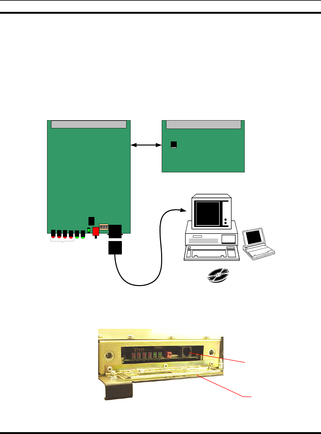
PERSONALITY PROGRAMMING
MM101271V1 R2A 57
8.1 PROGRAMMING A PERSONALITY
1. Install and run SitePro programming software TQ3408.
2. Connect one end of serial programming cable CA101302V1 (TQ3408) to the
computer (Figure 12 - Programming Hook-Up). Connect the other end of the
cable to the SitePro Controller Serial Programming Port J8 (Figure 13 - Location
of Serial Programming Port J8).
3. Proceed with personality programming by running the program as instructed in
Programming Manual MM101461V1.
CD ROM Programming
Disk
J7
S1 J8
D1 D2 D3 D4 D5 D8
S2
Dipswitch
Reset
Pushbutton
Status
LED's
L1 L2 L3 L4 E
T
H
0
E
T
H
1
D12
Power
LED
U14
Personality
EEPROM
CONTROLLER
BOARD A2
CB101069V1
J1
ANALOG
BOARD A4
CB101070V1
I2C
Programming Cable
CA101302V1
To COM Port
Personal
Computer
EEPROM
U34
Figure 12 - Programming Hook-Up
Figure 13 - Location of Serial Programming Port J8
(Front Left of SitePro Controller with Hinged Door Open)
Serial
Programming Port
J8
Hin
g
ed Door

TROUBLESHOOTING
58 MM101271V1 R2A
9.0 TROUBLESHOOTING
The most common causes for problems encountered with the SitePro Controller are
programming errors and interface connections.
9.1 ON SITE TROUBLESHOOTING
When troubleshooting a SitePro Controller on site:
1. Verify that all cables are properly connected and secure. Refer to the applicable
configuration manual.
2. Verify the SitePro Controller personality is properly programmed for the specific
application. Refer to the configuration manual and the software release notes.
3. If it is suspected that the SitePro Controller has failed, replace the controller with a
known good unit, properly programmed for this application.
4. If the replacement SitePro Controller resolves the problem, bench check the defective
unit using the test procedures provided in this manual or send it to the repair and
return depot.
9.2 IN CASE OF DIFFICULTY
If unable to resolve a problem satisfactorily, contact the M/A-COM Technical Assistance
Center (TAC) at 1 (800) 528-7711 (Outside USA, (434)-385-2400).
9.3 SITEPRO SHELF TEST
9.3.1 Equipment Needed
• 13.8V Power Supply (2A min)
• Current Meter
• PC with terminal emulator
• Loopback cables – described below
• Power Cable
• RJ-45 to PC serial cable
• RJ-11 to PC serial cable
Both serial cables are connected per the chart below. One cable is RJ-45 (8 pin modular)
to DB-9F. The other cable is RJ-11 (6 pin Modular) to DB-9F.
Table 20 - Cable Connections
SIGNAL RJ PIN DB-9F PIN SIGNAL
Tx 2 2 Rx
Rx 1 3 Tx
Gnd 3 5 Gnd
TROUBLESHOOTING
MM101271V1 R2A 59
1. Connect power (13.8V) to J7 on the rear of the shelf. Measure total shelf current.
Current should be within the limits shown in the table below. Connect +13.8VDC
to J7-1 and GND to J7-2.
Table 21 - Current (I) Limits
SHELF DESCRIPTION PART
NUMBER
MIN
CURRENT
MAX CURRENT
Fully loaded shelf EA101209V1 1.0A 1.4A
W/O RMIC and RM EA101209V2
W/O Analog Board EA101209V3
W/O both EA101209V4
2. Check that the Green front power light came on.
3. Check that ‘SITEPRO!’ appears on the front LED Display.
4. Check that the +5V, +12V, -12V, and CTS LEDs are lit on the (Rockwell Modem)
RMIC Board.
5. Set up a terminal emulator on PC COM1 for 38.4Kbaud, 1 start bit, no parity.
Connect the PC COM1 serial port to J8 (RJ-11modular jack) on the front of the
Controller Board.
6. Set up a second copy of the terminal emulator (or a second PC) connected to
COM2, 2400 baud, 7 bit, odd parity, connected to J14-I (80C323 Port0) (RJ-45
modular jack) on the rear of the shelf.
The tester should become familiar with the Factory Test program, which is stored
in the Controller boards when they arrive from the board manufacturer.
NOTE
Factory test software is available on a compact disc. The test software is loaded
serially like application code.
The test program will come up in non-menu mode after three PNG’s. There are
several modes. For manual test, get into menu mode by typing ENTER, then ‘q’,
then ‘m’.
Menu Mode – Runs automated tests from a menu. Some menus have sub menus.
‘0’ goes to Command mode.
Non-Menu Mode – Runs automated tests without displaying the menu (for
automated testing). ‘0’ goes to command mode.
Command mode – provides lower level control of board functions. See ‘H’ (help)
menu. ‘Q’ goes to menu mode.
7. Select test 4 (Modem board tests). Then select sub test 1 (Load a file to the Modem
board). Use the terminal emulator file transfer utility to send the file
‘SIMON.HEX’ to the Modem . The upload takes about 10 seconds. Hit ENTER.
The header **********SIMON SITEPRO 2001************’ should appear on
the second terminal.

TROUBLESHOOTING
60 MM101271V1 R2A
8. Get the Factory Test into Command Mode. Send the following commands.
SI2C 4C 01 02 (Sets up the I2C to address the I/O expander on the Analog Board)
WI2C 00 00 (Selects filter 0 and sets up normal path for RF data)
SI2C 50 01 00 (Sets up the I2C to address the Digital Pot on the Analog Board)
WI2C A9 50 (Sets the pot to normal level)
9.3.2 RF Data Loop Test
1. Connect a loopback plug(Figure 16 - Loopback Test Connectors) into J12 (EDACS
Connector) on the rear of the shelf (Refer to Figure 14 - RF Data Signal Path).
This plug loops pin 19 (MODULATION) to pin 7 (VOL/SQ/HI).
From terminal 2 type the command
POR1=EF (sets HSACQ0CTL) to 1 on the Analog board.
From terminal 2, type ‘BERDE-02=1’. In a few seconds, the response below will
appear on the terminal.
“ERROR COUNT = 0000 RECEIVE CHECKSUM = 027C11”
Sometimes the first line displayed is incorrect. Unit passes if the second line is
correct.
2. Hit the ESC key to stop the test.
9.3.3 Modem Loop Test
1. Connect a loopback plug into J4A (RM0) on the rear of the shelf (Refer to Figure 15
- Phone Line Data Signal Path).
This plug loops transmit to receive. It is made by tying wires together on an 8-pin
modular plug. Tie pin 2 to pin 4 and pin 3 to pin 5.
2. On the RMIC Board, set up Rx and Tx levels by closing sections 2 and 6 of switch
S1. Open all other sections
From terminal 1, in menu mode, execute test 4, subtest 3 (Dual Port Ram Test). This
resets the SitePro Modem Board. The SIMON turn-on banner will appear on terminal
2.
3. From terminal 2, type ‘MDS 1’.
4. From terminal 2, type ‘BERDE-0=1’. In a few seconds, the response below will
appear on the terminal.
“ERROR COUNT = 0000 RECEIVE CHECKSUM = 027C11”
Sometimes the first line displayed is incorrect. Unit passes if the second line is
correct.
5. Hit the ESC key to stop the test.
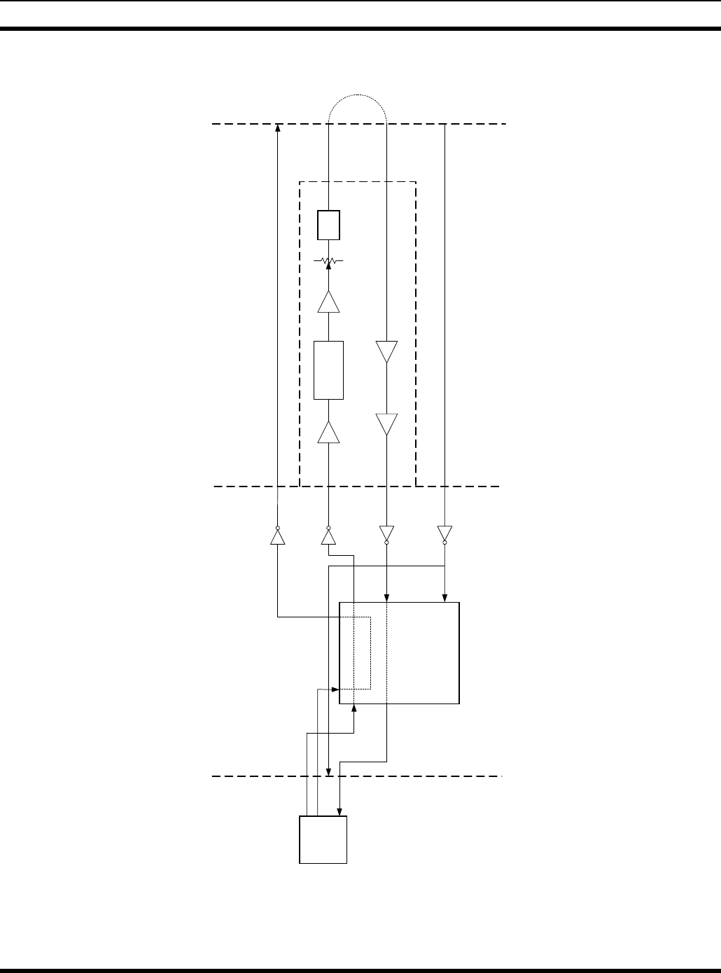
TROUBLESHOOTING
MM101271V1 R2A 61
RF MODEM
RFTXDAT
RFTXCLK
RFRXDAT
RFRXCLK
RFTXD
RFTXCLK
RFRXD RFRXDAT
RFRXCLK
RFTXCLK_OUT RFTXCLK
RFTXDAT +
AMP
-
FILTER MUX
AMP
ANALOG BOARD A4
AMP
++
SLICER
REAR OF
SHELF
INTERCONNECT BOARD A2CONTROLLER BOARD A2
SITEPRO MODEM BOARD A8
(Not Inverted)
(Not Inverted)
(Not Inverted)
PLD
LOOPBACK
PLUG
RF DATA SIGNAL PATH
J12
Figure 14 - RF Data Signal Path
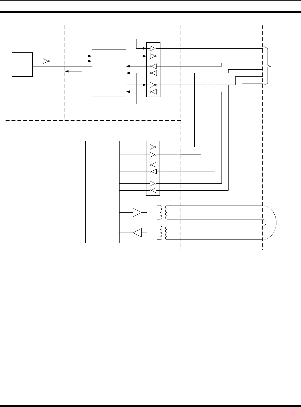
TROUBLESHOOTING
62 MM101271V1 R2A
PL MODEM
CONTROLLER BOARD A2
SITEPRO
MODEM BOARD
A8
PLTXDAT
PLTXCLK
PLRXDAT
PLD
PLTXD
PLTXCLK
PLRXD
PLRXCLK
PLTXDAT
PLRXDAT
PLRXCLK
RS-232
RTS
CTS
RJ45
REAR OF SHELF
ROCKWELL MODEM INTERFACE CARD A3
PLRXCLK
PLRXDAT
PLTXDAT
PLTXCLK
CTS
RTS
INTERCONNECT BOARD A1
ROCKWELL MODEM
AMP
AMP
TX
RX
+
-
-
+
PHONE LINE DATA SIGNAL
PATH
RS-232
LOOPBACK
PLUG
J4A
Figure 15 - Phone Line Data Signal Path
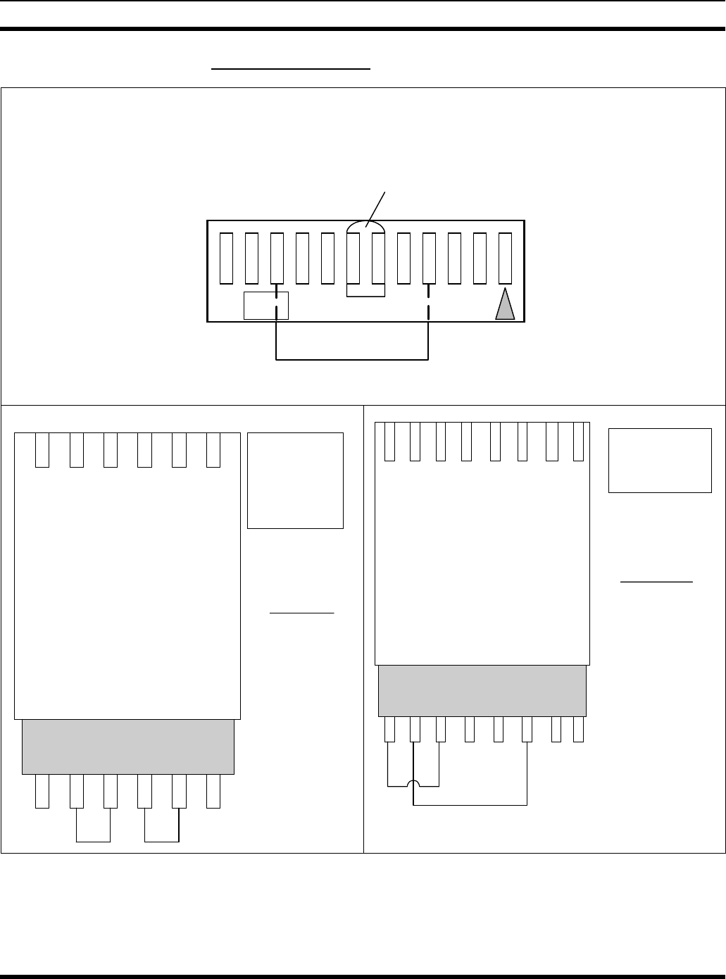
TROUBLESHOOTING
MM101271V1 R2A 63
9.3.4 Loopback Connectors
7135911131517192123
Jumper
TOP VIEW
Key
Test Location: Rear of shelf at connector J12
AMP
1
Make using AMP, 24 cavity connector number 102387-5
123456
RJ-11 Connector
Bottom View: Anchor Clip
on opposite side.
123456
At the rear of the
shelf, this test
connector inserts
into the jack
labelled "RM-0".
Pin Assignments:
1 - N/C
2 - RM-TX +
3- RM-TX -
4 - RM - RX -
5 - RM - RX +
6 - N/C
Jumpers
Bottom View/ (Side without anchor clip)
1234 5 6 7 8
RJ-45 Connector
12 3 6
Pin Assignments:
1- ETH TX +
2- ETH TX -
3- ETH RX +
4 - N/C
5 - N/C
6 - ETH RX -
7 - N/C
8 - N/C
Test Connector/Cable is
interchageable for
testing both ETH-0 &
ETH-1
Jumpers
Figure 16 - Loopback Test Connectors

TROUBLESHOOTING
64 MM101271V1 R2A
9.4 FIELD TROUBLESHOOTING GUIDE
9.4.1 SitePro Controller Board
This guide assumes the Controller board is in a SitePro shelf on a bench, not connected to
a station, but with 13.8V power applied to J7 of the shelf. It is also assumed that
‘FactoryTest’ software resides on the Controller. Modem board test program ‘SIMON’ is
also needed for some of the tests. In most cases, the shelf top cover must be removed.
See the Shelf Test Procedure for setup information and some information on FactoryTest.
Set up two terminal emulators as described in the Shelf test.
This is not a detailed test procedure. It is intended for use in service shops by technicians
having a high degree of expertise in troubleshooting electronic circuitry. Some circuits
cannot be tested at the shelf level.
9.4.1.1 REFERENCE DOCUMENTS
WD-CB101069V1 - Schematic Diagram
TS-CB101069V1 - Test Spec
AD-CB101069V1 - Assembly Drawing
Block Diagrams of Controller Board and SitePro Modem Board
9.4.1.2 BOARD WILL NOT RUN i.e. FACTORY TEST DOESN’T COME UP
Procedure:
After 3 PNGs appear on the terminal, wait about 10 seconds or until ‘F R1A01’ or later
version number appears on the display.
ENTER should put the FactoryTest software into Command mode. ‘q’ then ENTER takes
it to Non-menu mode, then ‘m’ followed by ENTER should produce the test menu. If no
response, turn power off then on and retry. If Boot/Loader comes up (> prompt), serially
load Factory Test.
Troubleshooting information:
Check 5V at TP6 and 3.3V at TP5.
If no voltage, check hot swap controller U37. U32-2 (ON) should be 5V, Mate-detect A
and B should both be grounded. U37-5 (FB) should be 1.3V. U37-6 (GATE) should be
about 16V.
If 5V is not seen on U42-2, then 555 timer U40 may be holding the ON pin low except
for momentary intervals every second or so.
There may be a problem in the serial port SMC1, which is used to interface to the test
system through the diagnostic connector J8 on the front of the board. This is a normal
serial port of the 860 processor. The J8 interface is RS232, which is converted to 3.3V
levels to the processor. SMC1TX originates from U1 (not accessible) at 3.3V level and
drives RS232 converter U36-17. U36-12 drives J8-2 at RS232 levels. Input from the
terminal comes in at RS232 levels to J8-1, which is fed to U24-5 where it is converted to
3.3V levels at U24-18 and goes to SMC1RX on U1 (not accessible).

TROUBLESHOOTING
MM101271V1 R2A 65
Check 29.4912 MHz oscillator Y2.
Check for wrong parts or misoriented parts.
Has PLD been programmed? Use FactoryTest Command mode command ‘R PLD_ID
ALL’ to check PLD version.
9.4.2 SitePro Modem Board Tests From The 860
9.4.2.1 CODE RAM TEST
Procedure:
Execute FactoryTest test 4, subtest 2.
Troubleshooting information:
Failure indicates problem is with U2 on the Modem board or associated circuitry U17 and
U18.
If Code RAM and DUAL PORT RAM test fail, there may be a bus problem. Test with a
known good Modem board to isolate the problem to the Controller or the Modem.
9.4.2.2 DUAL PORT RAM TEST
Procedure:
Execute Factory Test test 4, subtest 3.
Troubleshooting information:
Failure indicates a problem communicating with U3 on the Modem Board.
IF MODEM BOARD IS BAD
Check the Dual Port RAM U3 and Code RAM U2
The processor should be held reset during these tests. U1-10 should be HI (3.3V) to
reset.
IF CONTROLLER IS BAD
Check 14.7456MHz on J9-19.
Check Data bus activity on J9-1,2,3,4,33,34,35,36
Check address bus activity on J9-5 thru12, and 25 thru 32.
Check that DPR Chip Select is occurring on J9-15 during DPR test.
Check that Code RAM Chip Select is occurring on J9-14 during Code RAM test.
Check that RESET is HI (3.3V) on U1-10 during Code RAM test.
9.4.2.3 INTERRUPT FEATURE
Procedure:
Use FactoryTest test 4, subtest 1 to load ‘DCTEST.HEX’. Then execute FactoryTest test
4, subtests 4 and 5.

TROUBLESHOOTING
66 MM101271V1 R2A
Troubleshooting information:
Was ‘DCTEST’ loaded into the Modem daughter board?
Check DPR U3 on Modem Daughter Board. Pin 38 Interrupts the 80C323 on the Modem
Board. Pin 43 interrupts the 860. This test is an interaction between the Modem Board
and the Controller Board so testing with one known good board can isolate the problem.
9.4.3 Modem Board Tests Using Simon
9.4.3.1 LOAD SIMON
Procedure:
Use FactoryTest test 4, subtest 1 to load ‘SIMON.HEX’.
Troubleshooting information:
If SIMON loads properly, you will hear a beep or see the SIMON turn-on banner appear
on the terminal connected to 80C323 Port 0.
Failure to load code in the Modem board (applies to DCTEST also) could be due to
problems with Code RAM U2 and associated logic U17 and U18. Processor U1 must be
held reset (U1-10=3.3V) during a code load. It is unreset when ENTER is sent to Factory
Test after a download.
9.4.3.2 TEST DPR FROM THE MODEM SIDE
Procedure:
Execute SIMON Command ‘TMX 0-1FFD’.
Troubleshooting information:
Assuming SIMON loaded and is running, there must be a problem with DPR U3 or the
Microprocessor (U1)interface to it. Note: Use terminal 2 for SIMON commands.
9.4.3.3 TEST MODEM DATA SRAM
Procedure:
Execute SIMON Command ‘TMX 8000-FFFF’.
Troubleshooting information:
If SIMON is running, U4 is indicated.
9.4.3.4 MODEM BER TEST ON RF MODEM
Procedure:
This is the same test as the shelf RF loopback test. Execute SIMON Command BERDE-
02=1. Correct result is no errors and checksum=027C11.
Troubleshooting information:
SIMON causes a data stream to be generated in RF Modem U9 at U9-21 (RFTXDAT).
This data goes to the Controller Board on J2-30 where it enters the PLD at U27-122

TROUBLESHOOTING
MM101271V1 R2A 67
(RFTXD). It exits on U27-38 (RFTXDAT), is buffered and inverted by U29F, entering
on U29-13, exiting on U29-12. It exits the Board on J7-C23.
At the rear of the shelf, RFTXDAT is looped back into the Controller board on J7-C26
(RFRXDAT_FROM_SLICER). This signal is buffered and inverted by U29D, entering
on U29-9, exiting on U29-8, which drives into the PLD U27-53. It exits the PLD on U27-
99 (RFRXD). This goes to the Modem Board on J2-7. On the Modem Board, it goes to
U9-19 completing the loop.
Refer to RF Loop Test Block Diagram in the instruction book.
This test may fail due to problems in the microprocessor U1 interface to the Modem IC
U9. This includes 3V/5V converter U6, U21, U23, U16C and perhaps address decoder
U5 or U16A. Many negative going interrupt pulses should be seen on U9-24. Check R11.
9.4.3.5 MODEM BER TEST ON PL MODEM
Procedure:
This is the same as the shelf PL loopback test. Reset the Modem Board. SIMON
Commands are MDS1 then BERDE-01=1. Correct result is no errors and
checksum=027C11.
Troubleshooting information:
After running the BER test on the RF Modem (above), SIMON code requires a reset
before running the BER test on the Phone Line Modem. This can be accomplished by
using FactoryTest to execute test 4, subtest 3 (Dual Port RAM test). This will reset the
Processor then unreset it without affecting loaded code.
SIMON causes a data stream to be generated in PL Modem U10 at U10-21 (PLTXDAT).
This data goes to the Controller Board on J2-9 where it enters the PLD at U27-31
(PLTXD). It exits on U27-23 (PLTXDAT), is buffered, inverted and converted to RS232
levels by U30, entering on U30-7, exiting on U30-2. It exits the Board on J7-B19.
Data is passed through the Rockwell Modem then, at the rear of the shelf, PLTXDAT is
looped back through the Rockwell Modem and into the Controller board on J7-B21
(PLRXDAT). This signal is buffered, inverted and converted back to TTL levels by U30,
entering on U30-9, exiting on U30-8, which drives into the PLD U27-25. It exits the PLD
on U27-34 (PLRXD). This goes to the Modem Board on J2-29. On the Modem Board, it
goes to U10-19 completing the loop.
Refer to PL Loop Test Block Diagram in the instruction book.
This test may fail due to problems in the microprocessor U1 interface to the Modem IC
U10. This includes 3V/5V converter U6, U21, U23, U16C and perhaps address decoder
U5 or U16A. Many negative going interrupt pulses should be seen on U10-24. Check
R12
9.4.3.6 TEST LSDIN
Procedure:
Apply 100Hz 1VPP sine wave to J12-7. This should produce a 0 to 5V 100Hz square
wave at Controller Board connector J7-C10. Observe 3VPP 100Hz square wave at U1-2
on the Modem Board.
TROUBLESHOOTING
68 MM101271V1 R2A
Troubleshooting information:
LSDIN is input on J7-C10. It is buffered and inverted by U18D, entering on U18-9,
exiting on U18-8. It enters the PLD on U27-106 and exits on U27-98 (LSIN). It goes to
the Modem Board on J2-23. On the Modem board it is called LSRX and goes directly to
the processor U1-2 which is Port 1.0.
9.4.3.7 I/O OUTPUTS TEST - GROUP D
Procedure:
The table below gives the required SIMON commands to exercise each of these 3
outputs. It also lists the point to monitor. Use small size easy ball clips to reach the B row
of J7.
Table 22 - SIMON Commands
NAME SIMON COMMAND LO SIMON COMMAND HI MONITOR POINT
WAL1 POR3=FF POR3=CF J7-B15
WAL2 POR3=FF POR3=CF J7-B16
HSACQCTL POR1=FF POR1=ED J7-C8
Troubleshooting information:
This test checks the paths of 3 I/O signals which originate at the 80C323 Microprocessor
on the Modem Board, go down to the Controller Board, then through the PLD, then
through inverting buffers to the card edge. The paths are tabularized below.
Table 23 - I/O Signal Paths
NAME ORIG EXIT
MODEM
ENTER
PLD
EXIT
PLD
ENTER
BUF
EXIT
BUF
J7
PIN
EXIT
NAME
WAL1 U1-16 J2-16 U27-91 U27-81 U29-3 U29-4 J7-B15 WALSH1
WAL2 U1-17 J2-21 U27-90 U27-80 U29-5 U29-6 J7-B16 WALSH2
HSACQCTL U1-6 J2-15 U27-86 U27-45 U34-13 U34-12 J7-C8 HSACQ
9.4.3.8 TEST LSDOUT
Procedure:
Issue FactoryTest Command Mode command ’w pld_ctrl 0x00’.
Monitor Controller Board pin J7-C9.
Issue SIMON command POR3=FF to make the pin go LO.
Issue SIMON command POR3=EF to make the pin go HI.
Troubleshooting information:
This test checks the path of signal LSDOUT. It uses the WAL1 signal tested above to
generate a signal into the PLD. The signal exits the PLD at U27-110. It is buffered and
inverted by U32C, entering on U32-5, exiting U32-6 which drives off the board at J7-C9.

TROUBLESHOOTING
MM101271V1 R2A 69
9.4.3.9 ETHERNET TEST
Procedure:
Execute FactoryTest test 5, subtests 1 and 2.
Troubleshooting information:
The FEC is the 10/100 Base-T Ethernet port originating in the 860 MII port which
interfaces to Network PHY device U5. U5 drives transformer T1 which drives off the
board to Ethernet Port 0. Tx+ and Tx- are on pins J7-A2 and J7-A3. Rx+ and Rx- are on
pins J7-A5 and J7-A6.
SCC1 is the 10 Base-T Ethernet port originating in the 860 SCC1 port which interfaces to
Network PHY device U12. U12 drives transformer T2, which drives off the board to
Ethernet Port 1. Tx+ and Tx- are on pins J7-A8 and J7-A9. Rx+ and Rx- are on pins J7-
A11 and J7-A12.
Three tests are run on each Ethernet port.
The first test performs a loopback test entirely inside the 860 processor. It should never
fail.
The second test performs a loopback test inside the PHY chip. Failure indicates a
problem with the PHY chip or the connections from the 860 to the PHY.
The third test performs an external loopback test with the TX (+ and -) looped back to
RX (+ and -) using a loopback plug on the rear of the shelf. These connections must be
very short. If the first 2 tests pass, failure indicates problems with the transformer or the
connections from the PHY to the transformer, or the loopback plug.
9.4.3.10 LED TEST
Procedure:
Execute FactoryTest test 6.
Troubleshooting information:
I2C bus may be shorted. Check that SDA and SDL are normally 5V and bursts of data
and clock are seen when the test is run. Clock and data should show no appreciable rise
or fall times at a sweep rate of 100us per division. If other I2C devices are working, then
U15 is indicated.
9.4.3.11 DIPSWITCH TEST
Procedure:
Execute FactoryTest test 7.
Troubleshooting information:
If other I2C devices are working, then U26 is indicated, possibly pullup resistor pack
RN12 or bad switch S2.

TROUBLESHOOTING
70 MM101271V1 R2A
9.4.3.12 EEPROM LOAD TEST
Procedure:
Execute FactoryTest test 6, subtest 1.
Troubleshooting information:
If other I2C devices are working, then U14 is indicated.
9.4.3.13 DRAM TEST
Procedure:
Execute FactoryTest test 9.
Troubleshooting information:
Software is actually running out of DRAM. The test only checks that portion not being
used by the program. This is a test of U2 and U7.
9.4.3.14 FLASH TEST
Procedure:
Execute FactoryTest test 10.
Troubleshooting information:
Test software is stored in the Flash memory so the test only checks that portion not
holding code. This is a check of U10 and U11.
9.4.3.15 TEST SERIAL PORT QUART C
Procedure:
Connect terminal to J14C on the rear of the shelf. Set terminal for 9600 baud, N81. Type
a few characters and observe characters echoed to terminal.
Troubleshooting information:
The QUART is U28. Its four serial ports are used for BSL0, BSL1, QUART PORT C,
and QUART PORT D. If the other ports are working, the problem may be in the RS232
converter U36. RS232 level input comes on the Controller board at J7-A25, is fed to
U36-8, converted to 3.3V levels at U36-21, to the QUART U28-25. The QUART should
echo the characters out of TXC, U28-26, to U36-24, and it should appear at RS232 levels
at U36-5 and J7-A26.
9.4.3.16 TEST SERIAL PORT QUART D
Procedure:
Connect terminal to J14D on the rear of the shelf. Set terminal for 9600 baud, N81. Type
a few characters and observe characters echoed to terminal.

TROUBLESHOOTING
MM101271V1 R2A 71
Troubleshooting information:
The receive path is J7-A27 to U36-9 at RS232 level, out U36-20 at 3.3V level, to
QUART U28-27, echoed out U28-28 to U36-23, and out U36-6 to J7-A28 at RS232
level.
9.4.3.17 BSL TEST
Procedure:
Loop BSL0 to BSL1 and run FactoryTest test 11, subtest 1.
Troubleshooting information:
+12V must be present for the BSL circuits. Two separate tests are run; first BSL0 to
BSL1 then BSL1 to BSL0.
Two ports of QUART U28 are used. Port A receives and transmits on BSL0. Port B
receives and transmits on BSL1.
The path for the first test begins at QUART TXDA U28-6. This is inverted in U35A
which drives FET driver Q4. BSL0 is looped to BSL1 at J4C and J4D on the rear of the
shelf, so that signal appears at BSL1 input U23-3. This is inverted twice and converted to
a 3.3V level by U23B and Q10, which drives QUART PORT B input U28-14.
The path for the second test begins at QUART TXDB U28-15. This is inverted in U35B,
which drives FET driver Q3. BSL1 is looped to BSL0 at J4C and J4D on the rear of the
shelf, so that signal appears at BSL0 input U23-1. This is inverted twice and converted to
a 3.3V level by U23A and Q9, which drives QUART PORT A input U28-5.
9.4.3.18 TEST SCC2
Procedure:
Connect terminal to J14F on rear of shelf. Set terminal for 38.4kbd, N81. Type a few
characters and observe characters echoed to terminal.
Troubleshooting information:
This is a normal serial port of the 860 processor. The card edge interface is RS232, which
is converted to 3.3V levels to the processor. SCC2RX comes in to the Controller Board
on J7-A19. This RS232 signal comes in to U24-7, gets converted to 3.3V levels at U24-
16 and goes to SCC2RX on U1 (not accessible).
The 860 processor U1 (not accessible) echoes characters out SCC2TX at 3.3V level and
drives RS232 converter U24-13. U24-10 drives out to the card edge (J7-A20) at RS232
levels.
9.4.3.19 TEST SCC3
Procedure:
Connect terminal to J14G on rear of shelf. Set terminal for 38.4kbd, N81. Type a few
characters and observe characters echoed to terminal.
Troubleshooting information:
This is a normal serial port of the 860 processor. The card edge interface is RS232, which
is converted to 3.3V levels to the processor. SCC3RX comes in to the Controller Board

TROUBLESHOOTING
72 MM101271V1 R2A
on J7-A21. This RS232 signal comes in to U24-6, gets converted to 3.3V levels at U24-
17 and goes to SCC3RX on U1 (not accessible).
The 860 processor U1 (not accessible) echoes characters out SCC3TX at 3.3V level and
drives RS232 converter U24-14. U24-9 drives out to the card edge (J7-A22) at RS232
levels.
9.4.3.20 TEST SMC2
Procedure:
Connect terminal to J14H on rear of shelf. Set terminal for 38.4kbd, N81. Type a few
characters and observe characters echoed to terminal.
Troubleshooting information:
This is a normal serial port of the 860 processor. The card edge interface is RS232, which
is converted to 3.3V levels to the processor. SMC2TX originates from U1 (not
accessible) at 3.3V level and drives RS232 converter U24-12. U24-11 drives out to the
card edge at RS232 levels. The fixture loops TX to RX so the RS232 signal comes back
into U24-8, gets converted to 3.3V levels at U24-15 and goes to SCC3RX on U1 (not
accessible).
This is a normal serial port of the 860 processor. The card edge interface is RS232, which
is converted to 3.3V levels to the processor. SMC2RX comes in to the Controller Board
on J7-A17. This RS232 signal comes in to U24-8, gets converted to 3.3V levels at U24-
15 and goes to SMC2RX on U1 (not accessible).
The 860 processor U1 (not accessible) echoes characters out SMC2TX at 3.3V level and
drives RS232 converter U24-12. U24-11 drives out to the card edge (J7-A18) at RS232
levels.
9.4.3.21 I/O OUTPUTS TEST - GROUP A
Procedure:
To test each output, the FactoryTest Manual Mode Command is given to cause the
monitor point to go high or low. Connect a 10K pullup resistor from the monitor point to
5V in order to see the result. J11 is on the rear of the shelf.
Table 24 - FactoryTest Manual Mode Commands
SIGNAL
NAME
10K
PULLUP
REQUIRED
COMMAND
HIGH
COMMAND
LOW
MONITOR
POINT
CPPTOUT yes W stn_ctrl 0x00 W stn_ctrl 0xFF J11-6
TXCGDIS yes W stn_ctrl 0x00 W stn_ctrl 0xFF J11-7
RPT_INH yes W stn_ctrl 0x00 W stn_ctrl 0xFF J11-3
RPTKEY yes W stn_ctrl 0x00 W stn_ctrl 0xFF J11-5
SPARE1 yes W stn_ctrl 0x00 W stn_ctrl 0xFF J11-1
SPARE2 yes W stn_ctrl 0x00 W stn_ctrl 0xFF J11-2
TROUBLESHOOTING
MM101271V1 R2A 73
Troubleshooting information:
Each output in Group A is written to a PLD register by the 860 processor. Its path to the
card edge is shown below. They all come out of the PLD, are buffered and go to a pin on
J7.
Table 25 - I/O Output Group A Paths
I/O OUTPUTS GROUP A PATHS
SIGNAL NAME PLD PIN BUFFER IN BUFFER OUT J7 PIN
CPPTOUT 28 U34-1 U34-2 J7-B13
TXCGDIS 70 U34-11 U34-10 J7-B2
RPT_INH 103 U34-9 U34-8 J7-A13
RPTKEY 111 U33-11 U33-10 J7-B10
SPARE1 100 U34-3 U34-4 J7-A7
SPARE2 101 U33-13 U33-12 J7-A10
9.4.3.22 I/O OUTPUTS TEST - GROUP B
Procedure:
To test each output, the FactoryTest Manual Mode Command is given to cause the
monitor point to go high or low. Some outputs will require a 10K pullup resistor to 5V to
be seen.
Table 26 - FactoryTest Manual Mode Commands (Group B)
SIGNAL NAME 10K
PULLUP
REQUIRED
COMMAND
HIGH
COMMAND
LOW
MONITOR
POINT
SYNTH_CLK yes W synth_ctrl 0x00 W synth_ctrl 0xFF J12-13
SYNTH_DATA no W synth_ctrl 0x00 W synth_ctrl 0xFF J12-14
SYNTH_LD_EN yes W synth_ctrl 0x00 W synth_ctrl 0xFF J12-15
EMSQTOAV no W voter_ctrl 0xFF W voter_ctrl 0x00 J12-17
RX_MUTE no W rx_ctrl 0x00 W rx_ctrl 0xFF J12-11
REMRPT yes W rx_ctrl 0x00 W rx_ctrl 0xFF J12-3
SYNTH_DATA is internally pulled to +12V.
With no load, EMSQTOAV will pull up to +12V.
RX_MUTE will pull to +8V.
Troubleshooting information:
Each output in Group B is written to a PLD register by the 860 processor. Its path to the
card edge is shown below. They all come out of the PLD, are buffered and inverted and
go to a pin on J7.
TROUBLESHOOTING
74 MM101271V1 R2A
Table 27 - I/O Outputs Group B Paths
I/O OUTPUTS GROUP B PATHS
SIGNAL NAME PLD PIN BUFFER IN BUFFER OUT J7 PIN
SYNTH_CLK 87 U33-5 U33-6 J7-C4
SYNTH_DATA 88 U33-3 U33-4 J7-C5
SYNTH_LD_EN 102 U35-13 U35-12 J7-C6
EMSQTOAV 97 U35-5 U35-6 J7-C3
RX_MUTE 112 U33-9 U33-8 J7-B9
REMRPT 96 U35-11 U35-10 J7-B6
Note that EMSQTOAV goes through an additional transistor Q8.
Note that RX_MUTE goes through an additional transistor Q1.
9.4.3.23 I/O OUTPUTS TEST - GROUP C
Procedure:
To test each output, the FactoryTest Manual Mode Command is given to cause the
monitor point to go high or low. Some outputs will require a 10K pullup resistor to 5V to
be seen.
Table 28 - FactoryTest Manual Mode Commands (Group C)
SIGNAL
NAME
10K
PULLUP
REQUIRED
COMMAND
HIGH
COMMAND
LOW
MONITOR
POINT
STNPTT Yes W rx_ctrl 0x00 W rx_ctrl 0x0C J12-2
A/DMODCTL No W rx_ctrl 0x00 W rx_ctrl 0x0C J12-4
Troubleshooting information:
Each output in Group C is written to a PLD register by the 860 processor. Its path to the
card edge is shown below. They both come out of the PLD, are buffered and inverted and
go to a pin on J7.
Table 29 - I/O Outputs Group C Paths
I/O OUTPUTS GROUP C PATHS
SIGNAL NAME PLD PIN BUFFER IN BUFFER OUT J7 PIN
STNPTT 71 U34-5 U34-6 J7-A14
A/DMODCTL 72 U29-11 U29-10 J7-A16
TROUBLESHOOTING
MM101271V1 R2A 75
9.4.3.24 I/O INPUTS TEST - GROUP A
Procedure:
To test inputs, it is necessary to apply 5V (through a 10K resistor) or ground to the input
point. Then execute a FactoryTest Command Mode READ command. The table shows
the command and expected result for both 5V input and ground input. The READ
command presents values in hex. Convert the hex to binary to see the individual bits. ‘x’
means ‘don’t care’
Table 30 - FactoryTest Command Mode READ Commands
SIGNAL NAME INPUT
POINT
COMMAND 5V
RESULT
GROUND
RESULT
SYNTH_LOCK_DET J12-12 R portb all xxxxxxx0 xxxxxxx1
SIMULCAST_INH J12-18 R portb all xxxxxx0x xxxxxx1x
REM_AUDIO_PRESENT J12-10 R portb all xxxxx0xx xxxxx1xx
PAFAIL J12-6 R portb all xxxx0xxx xxxx1xxx
RUSIN J12-9 R portb all xxx0xxxx xxx1xxxx
BYPASS J13-20 R portb all 0xxxxxxx 1xxxxxxx
The relays on the Analog board will operate when BYPASS is grounded.
Troubleshooting information:
Each of the signals in Inputs Group A originates off board as a TTL level signal, then
goes through a buffer and then to the PLD U27. The PLD interfaces to the 860 via the
processor bus. Levels into the PLD are 0 and 5V.
Table 31 - Group A I/O Input Paths
I/O INPUTS GROUP A PATHS
SIGNAL NAME J7 PIN BUFFER
IN
BUFFER
OUT
PLD PIN
SYNTH_LOCK_DET J7-C7 U23-9 U23-8 118
SIMULCAST_INH J7-B12 U23-11 U23-10 117
REM_AUDIO_PRESENT J7-B14 U18-1 U18-2 109
PAFAIL J7-B4 U18-11 U18-10 78
RUSIN J7-B8 U29-1 U29-2 75
BYPASS J7-B5 U23-13 U23-12 116
9.4.3.25 I/O INPUTS TEST - GROUP B
Procedure:
To test inputs, it is necessary to apply 5V ( in some cases, open) then ground to the input
point and then execute some FactoryTest manual mode commands. Results for
EXTPTTIN, EXTADIN, and EXT150IN are voltages measured on the given pin. Results
TROUBLESHOOTING
76 MM101271V1 R2A
for the other 3 inputs are read by the software by executing a FactoryTest Command
Mode READ command. The table shows the commands and expected result for both 5V
input and ground input.
Table 32 - READ Commands and Expected Results
SIGNAL NAME INPUT
POINT
COMMAND MONITOR
POINT
5V
RESULT
GROUND
RESULT
EXTPTTIN J13-6 W pld_ctrl 0x00
W rx_ctrl 0x80
J12-2
Requires pullup
5V
see note 1
0V
EXTADIN J13-5 W pld_ctrl 0x00
W rx_ctrl 0x80
J12-4 5V
see note 1
0V
EXT150IN See note 2 W pld_ctrl 0x00
W rx_ctrl 0x80
J7-C9
(Lsdout)
5V 0V
RCVNG_FROM_AV J7-C2 R voter_input all - Xxxxxxx0 Xxxxxxx1
CAS J11-8 R voter_input all - Xxx0xxxx Xxx1xxxx
CGMON J11-4 R voter_input all - Xx0xxxxx Xx1xxxxx
1. For EXTPTTIN and EXTADIN, just leave input open for’5V’ result.
2. For EXT150IN, for ‘5V result’, apply ground to J13-15 and 5V through a 10K
resistor to J13-16. For ‘Ground Result’, swap inputs.
3. RCVNG_FROM_AV is not used in the shelf. Apply inputs to the card connector J7.
Troubleshooting information:
Each input in Group B originates externally as a TTL level signal. It is buffered and
inverted and fed into the PLD. There, it can be read by the 860 processor. Its path from
the card edge to the PLD is shown below.
Table 33 - I/O Input Group B Paths
I/O INPUTS GROUP B PATHS
SIGNAL NAME ORIGIN BUFFER
IN
BUFFER
OUT
PLD PIN
EXTPTTIN J7-C11 U22-3 U22-4 67
EXTADIN J7-C12 U22-5 U22-6 60
EXT150IN J7-C13 U22-9 U22-8 68
RCVNG_FROM_AV J7-C2 U23-5 U23-6 119
CAS J7-B7 U18-3 U18-4 108
CGMON J7-B3 U18-5 U18-6 107
9.4.3.26 TEST PLRTS AND PLCTS, VDIRTS AND VDICTS
Procedure:
Jumper PLRTS to PLCTS, J14A-6 to J14A-7 on the shelf rear.

TROUBLESHOOTING
MM101271V1 R2A 77
Jumper VDIRTS to VDICTS, J14B-6 to J14B-7 on the shelf rear.
Then execute FactoryTest test 16.
Troubleshooting information:
Upon command of the 860 processor, PLRTS is generated in the PLD and exits U27-65.
It is buffered, inverted and converted to RS232 levels by U13, entering U13-11, exiting
U13-14. It exits the board on J7-B18.
PLRTS is looped back to the Controller board into PLCTS on J7-B17. It is converted to
TTL, buffered and inverted by U13, entering U13-13 and exiting U13-12. It enters the
PLD on U27-83 where it can be read by the 860 processor.
Upon command of the 860 processor, VDIRTS is generated in the PLD and exits U27-63.
It is buffered, inverted and converted to RS232 levels by U13, entering U13-10, exiting
U13-7. It exits the board on J7-C18.
VDIRTS is looped back to the Controller board into VDICTS on J7-C17. It is converted
to TTL, buffered and inverted by U13, entering U13-8 and exiting U13-9. It enters the
PLD on U27-82 where it can be read by the 860 processor.
9.4.3.27 PHASE LOCKED LOOP TEST AND TXC_MISSING_ALARM TEST
Procedure:
Use a Function Generator to produce a 0V to 5V 9600Hz square wave. Apply this across
J13-13 & 14 (9.6REF+ and -), with the ground side connected to J13-14.
Execute FactoryTest test 14, subtest 1. Ignore the first line of the on screen instructions
since the input is applied differently. Use a dual trace scope as described to check for two
signals in phase. RFTXCLK is also seen at J11-14.
Troubleshooting information:
This test uses PLL IC U16 to phase lock the RFTXCLK used by the RF Modem U9 on
the SitePro Modem Board to an external reference signal 9.6REFIN. The PLL chip
generates an 11.0592 MHz clock slaved to the external reference. In the PLD, this clock
is switched to the Modem board instead of the 11.0592 MHz. oscillator clock. Modem
Board IC U9 divides the 11.0592 MHz back down to 9.6kHz (RFTXCLK) which is
phased locked by the PLL U16. Both the reference and the feedback signals are switched
to the PLL inside the PLD.
A Modem board must be present for this test and it must not be held reset. The Modem
board is normally held reset by the Controller until it is explicitly unreset. It can be
unreset by loading code such as SIMON to it. It can also be unreset by executing Factory
Test 4, subtest 3, (Test Dual Port RAM).
9.6REFIN enters the Controller board at TTL levels on J7-C15. It is buffered and
inverted by U22F, entering in U22-13, exiting on U22-12. It enters the PLD on U27-69.
RFTXCLK is derived from the 11.0592 MHz clock on the Modem Board by U9, exiting
on U9-27. It is routed to the Controller board through J2-8 (Modem board) which
connects to Controller Board J2-8. It enters the PLD on U27-128.
If the loop fails to lock, one or both signals 9.6REFIN or RFTXCLK may not be getting
to the PLL U16. U16 or some of the associated components may be wrong, misoriented

TROUBLESHOOTING
78 MM101271V1 R2A
or missing. Use a known good Modem board. Check for 11.0592 MHz clock at Modem
Board U9-16.
Procedure:
Instead of following the on screen directions, observe TXC_MISSING_ALARM at J13-
18. The test requires an external pullup resistor.
Remove the 9.6REF signal. TXC_MISSING_ALARM should go high.
Troubleshooting information:
TXC_MISSING_ALARM is generated inside the PLD if 9.6REFIN is missing.
9.6REFIN must get to the PLD via the path described above. The
TXC_MISSING_ALARM signal exits the PLD on U27-62. It is buffered and inverted by
U35D, entering on U35-9, exiting U35-8.
9.4.3.28 TEST PLTXCLK
Procedure:
Observe PLTXCLK (9600Hz, RS232) at J14A-4 on the rear of the shelf.
Troubleshooting information:
PLTXCLK is generated on the Modem Board at U10-27, and is inverted by U24 before
exiting the Modem Board on J2-28. It enters the PLD on U27-32. It is also buffered,
inverted, and converted to RS232 levels by U30, entering at U30-6, exiting U30-3. It
exits the Controller Board on J7-B20.
A working Modem board must be present and not reset for this test.
9.4.3.29 TEST VDITXCLK
Procedure:
Observe VDITXCLK (9600Hz, RS232) at J14B-4 on the rear of the shelf.
Troubleshooting information:
This test checks the path of VDITXCLK. It is generated on the Modem Board at U11-27,
and is inverted by U25 before exiting the Modem Board on J2-11. It is buffered, inverted,
and converted to RS232 levels by U30, entering at U30-21, exiting U30-28. It exits the
Controller Board on J7-C20.
A working Modem board must be present and not reset for this test.
9.4.3.30 FSL OUTPUT TEST
Procedure:
Execute FactoryTest test 15
Observe the FSL output at J4C-4 on the rear of the shelf.
Troubleshooting information:
The FSL signal is a series of negative going 12V to 0V pulses occurring every 30ms and
2.5ms wide.
The FSL output signal is generated in the PLD using RFTXCLK (tested above) from the

TROUBLESHOOTING
MM101271V1 R2A 79
Modem Board. A working Modem board must be present and not reset for this test.
The FSL signal exits the PLD at U27-113. It is buffered and inverted by U33, entering at
U33-1, exiting U33-2 which drives FET driver Q2. The FET drives a +12V to 0V signal
to J7-C30. The FSL output is capable of driving a 50 ohm load resistor pulled to +12V.
9.4.3.31 EEPROM VERIFY TEST
Procedure:
After turning power off for a few seconds, then back on, execute FactoryTest test 8,
subtest 2.
Troubleshooting information:
If other I2C devices (LEDs, dipswitch) are working, failure of this test indicates a
problem with U14. This test is run after power is turned off and back on. FactoryTest test
8, subtest 1 must have been run previously. The EEPROM should retain its data with
power off.
9.4.4 Analog Board
This guide assumes the Analog board is in a SitePro shelf on a bench, not connected to a
station, but with +13.8VDC power applied to J7 of the shelf. It is also assumed that
‘FactoryTest’ software resides on the Controller board to provide control of the Analog
board. Modem board test program ‘SIMON’ is also needed for some of the tests. Two
Terminal emulators are needed. See shelf test.
This is not a detailed test procedure. It is intended for use in service shops by technicians
having a high degree of expertise in troubleshooting electronic circuitry.
9.4.4.1 REFERENCE DOCUMENTS
WD-CB101070V1 - Schematic Diagram
TS-CB101070V1 - Test Spec
AD-CB101070V1 - Assembly Drawing
Block diagram of Analog Board (Figure 11 - Analog Board Block Diagram)
9.4.4.2 TEST 2 - VOLTAGES
Measure +5V at C54(+). Measure +12V at C57(+). Measure –12V at C59(-). Measure –
5V at TP31.
If -5V is wrong voltage or missing, check U2.
9.4.4.3 TEST 3 - CLOCK FREQUENCY
Clocks are derived from a 400kHz oscillator Y1, U32C and U32D. Check for 400 kHz at
TP10. U3 divides the 400 kHz down to 25 kHz at TP11 and 3.125 kHz at TP12.
9.4.4.4 TEST 4 - SLICER
Input signal, 1000Hz sine wave at 1VPP, is applied to VOLSQHI and is buffered by
U15A. The same signal should be seen at TP13. The signal is then sliced by comparator
U33A and a squared wave (0 to 5V) should be seen at RFRXDAT. Bias on U33-2 is
around 2.5V. Problems with U31 can affect the bias.
TROUBLESHOOTING
80 MM101271V1 R2A
9.4.4.5 TEST 5 - LOW SPEED DECODE FILTER
Sine wave input 100Hz at 1VPP at VOLSQHI is buffered by U15A (seen at TP13),
amplified about 2:1 in U15B (seen at TP15), passes through high pass filter U16 (seen at
TP16), then through low pass filter U14 (seen at TP17), through amplifier (gain = 2)
U28A (seen at TP18). The frequency response is measured at TP18 before going to
nonlinear circuits. U12B is a slicer, which converts the waveform to a square signal at
TP14. Q1 interfaces the squared waveform to a microprocessor on another board. Note
that a 10K pullup to +5V is needed on LSIN to see the 0 to 5V output. This resistor is on
the Controller board.
The LS Decode filter frequency response (shown below) is entirely determined by U16
(rolloff below 50Hz) and U14 (rolloff above 250Hz).
Frequency Output
100 Hz 0 db (ref)
50 Hz -3 db ± 1db
18 Hz -35 db ±- 3db
250 Hz -0 db ±- 1db
300 Hz <-40db
With 1V P-P 100Hz in to VOLSQHI, the levels at various test points are shown in the
table below.
Table 34 - Test Point Levels
TEST POINT VOLTAGE SIGNAL TYPE
TP13 1 V P-P (2.5VDC bias) Sine
TP15 2.2V P-P Sine
TP16 2.2V P-P Sine
TP17 2.2V P-P Sine
TP18 4.4V P-P Sine
TP14 12.6 V P-P (+0.6 to –12V) Squared
LSIN w 10K pullup 5V P-P (0 to 5V) Squared
9.4.4.6 TEST 6 - LOW SPEED ENCODE FILTER
In the shelf, signals cannot be injected directly to the encode filter. One method of
driving the filter is to use the shelf EXT 150HZ input. Connect a 100Hz 1Vp-p square
wave signal across 150HZ+ to 150HZ- (J13-15 to 16). Make necessary PLD connections
with the commands:
W PLD_CTRL 0X00
W RX_CTRL 0X80
Configure the Analog board to use the 150HZ input with the commands
SI2C 4C 01 02
WI2C 10 00
TROUBLESHOOTING
MM101271V1 R2A 81
150Hz input is selected by mux U22 which is controlled by LSCTL. This signal is
derived from I2C I/O expander U4 (TP30) and must be logic 1 (5V) to select the 150HZ
input.
The signal then passes through amplifier U19A where it is reduced in level by about a
factor of 4 as seen at TP23. It then goes through buffer U19B (seen at TP22). Then
through low pass filter U20 (seen at TP21) then through final amplifier/buffer U17A.
Filtered output is seen at LSDTX.
Frequency response at LSDTX is entirely determined by U20 and associated components
and by the 25kHz clock.
Table 35 - Frequency Response at LSDTX
FREQUENCY RESPONSE
100 Hz (ref) 0 dB
200 Hz -3 dB
250 Hz -4 dB
300 Hz < -40 dB
With 100Hz 5Vp-p square wave into 150HZ input (J1-B19), levels through the circuit are
shown in the table below.
Table 36 - Circuit Levels
TEST POINT VOLTAGE SIGNAL TYPE
TP23 1 VP-P Square
TP22 1 VP_P Rounded Square
TP21 1.25VP-P Sine
LSDTX 4.4VP-P
(bias may vary)
Sine
9.4.4.7 TEST 8 - A/D CONVERTER
The A/D converter U23 is an I2C device with slave address 9E hex. If other I2C devices
are working, then U23 is the only IC involved in this test. Apply DC levels between 0V
and 5V to J12-1 (PA_SENSE) and read appropriate digitized results.
SI2C 9E 02 01
WI2C 00 01
RI2C 00 01 (second byte is the result)
9.4.4.8 TEST 10 - 9600 BAUD WIDE BAND HS FILTER
With the Analog board in the shelf, external signals cannot be applied directly to the High
Speed filter sections. Data can be generated by the RF Modem to produce a signal
through the filters. If response problems are suspected, inspect for broken, wrong, or
unsoldered components around the appropriate section of the ‘Quad Op Amp’ circuitry.
The response is entirely determined by this section.

TROUBLESHOOTING
82 MM101271V1 R2A
Two terminal emulators are required. Refer to the Shelf test. Load SIMON into the
Modem Board.
Select the filter with I2C commands
SI2C 4C 01 02
WI2C 00 00 (for filter 0)
WI2C 01 00 (for filter 1) Etc.
Set digital pot level with I2C commands
SI2C 50 01 00
WI2C A9 50 (for pot level of 50 hex)
The command ‘W RX_CTRL 0X00’ may also be needed to set up connections in the
PLD.
Run the RF BER test as described in the shelf test to produce data through the High
Speed filters.
Data is coupled to RFTXDAT (J1-A10), is buffered by U6A (seen at TP1) then is fed to
five separate filters.
One of the filters is selected by mux U7, which is controlled by three I2C select lines
HS_FILTER_SEL0, 1, and 2. These three select lines are outputs of I2C I/O expander
U4. The three filter select lines can be seen at TP19, TP24, and TP25. Note that if input
6, 7, or 8 is selected, no output will be present.
If all three select lines are logic 0, then filter 0 (9600 Baud Wide Band) is selected.
The mux output goes to digital pot U8, which is also an I2C device and is set to a value
of 50 (hex) for this test. Signal then passes through amplifier U6B (seen at TP9), then
through output mux U9 to output MOD (J1-A12). A scope will show the eye pattern at
TP9 or MOD.
U9 is controlled by select line MODCTL which is derived from I2C I/O expander U4
(TP28). MODCTL = 0 selects the path from the filters. Control of this bit is included
above in the filter selection command.
Typical signal levels are shown below for High Speed data input from the RF Modem.
Levels are also shown at TP9 when each of the other four filters is selected.
Table 37 - High Speed Data Signal Levels
TEST POINT VOLTAGE
TP1 5V pp
TP9 - filter 0 1.1vrms
MOD 1.1vrms
TP9 - filter 1 0.9vrms
TP9 - filter 2 0.95vrms
TP9 - filter 3 0.8vrms
TP9 - filter 4 0.9vrms
TP9 – filter 5, 6, 7 0

TROUBLESHOOTING
MM101271V1 R2A 83
9.4.4.9 TEST 11 - 9600 BAUD WIDE BAND ETSI HS FILTER
Same as test 10 except filter 1 (9600 Baud Wide Band ETSI) is selected by mux U7.
HS_FILTER_SEL0 is logic 1 and the other two are logic 0. See test 10 for levels.
9.4.4.10 TEST 12 - 4800 BAUD NARROW BAND HS FILTER
Same as test 10 except filter 2 (4800 Baud Narrow Band) is selected by mux U7.
HS_FILTER_SEL1 is logic 1 and the other two are logic 0. See test 10 for levels.
9.4.4.11 TEST 13 - 4800 BAUD NARROW BAND ETSI HS FILTER
Same as test 10 except filter 3 (4800 Baud Narrow Band ETSI) is selected by mux U7.
HS_FILTER_SEL2 is logic 0 and the other two are logic 1. See test 10 for levels.
9.4.4.12 TEST 14 - 9600 BAUD NARROW BAND HS FILTER
Same as test 10 except filter 4 (9600 Baud Narrow Band) is selected by mux U7.
HS_FILTER_SEL2 is logic 1 and the other two are logic 0. See test 10 for levels.
9.4.4.13 TEST 15 - I2C POT
This test checks I2C pot U8 at various settings. If High Speed filter tests have passed,
then U8 is the only IC involved in this test. The path is set up just as in test 10 and several
pot settings are checked at the output MOD. Failure means U8 is not responding to I2C
commands.
I2C commands:
SI2C 50 01 00
WI2C A9 XX (XX can be from 00 to FF hex)
9.4.4.14 TEST 16 - ANALOG AUDIO PATH
This test is similar to test 10 in that the path is set up exactly like test 10 with the same
input and output. The output mux is then switched to the ANALOG_AUDIO input.
SI2C 4C 02 01
WI2C 40 00
Output at MOD should drop to 0V since it is unconnected. Applying a signal to
ANALOG_AUDIO (J12-20) should then produce an output at MOD.
If tests 10-14 have passed and this test fails, U9 is suspected.
9.4.4.15 TEST 17 - RS232 TO RS485 CONVERSION OF PLTXDAT
Note: The remaining Analog board tests check circuitry that is only used in Simulcast
Systems.
A 9600 baud RS232 level signal is connected to PLTXDAT in the shelf. U24 converts it
to TTL at U24-12. This signal is fed to RS485 converter U25 at U25-1. Connect a 100
ohm load across PLTXDAT+ to PLTXDAT-. A differential signal of several volts should
be seen across PLTXDAT- to PLTXDAT+ (J13-7 to 8).
Generate the data signal with the SIMON commands below after resetting the Modem
board.
MDS1
BERDE-0=10

TROUBLESHOOTING
84 MM101271V1 R2A
9.4.4.16 TEST 18 - RS232 TO RS485 CONVERSION OF PLTXCLK
In the shelf, a 9600Hz RS232 level clock is always present at PLTXCLK. U24 converts it
to TTL at U24-9. This signal is fed to RS485 converter U25 at U25-7. Connect a 100
ohm load across PLTXCLK+ to PLTXCLK-.A differential signal of several volts should
be seen across PLTXCLK- to PLTXCLK+ (J13-9 to 10).
9.4.4.17 TEST 19 - RS485 TO TTL CONVERSION OF 150HZ
A 9600Hz differential signal is fed into converter U26 across inputs 150HZ+ and 150Hz-.
A single ended TTL level signal should appear at EXT 150 HZ (J1-C20). The differential
output of Test 18 is an appropriate input for this test.
9.4.4.18 TEST 20 - RS485 TO TTL CONVERSION OF 9.6_DATA
A 9600Hz differential signal is fed into converter U26 across inputs 9.6 DATA+ and 9.6
DATA-. A single ended TTL level signal should appear at EXT 9.6 DATA (J1-C16). The
differential output of Test 18 is an appropriate input for this test.
9.4.4.19 TEST 21 - RS485 TO TTL CONVERSION OF 9.6_REF
A 9600Hz differential signal is fed into converter U26 across inputs 9.6 REF+ and 9.6
REF-. A single ended TTL level signal should appear at EXT 9.6 REF (J1-C12). The
differential output of Test 18 is an appropriate input for this test.
9.4.4.20 TEST 22 - RELAY CONTINUITY
Relay K1 and K2 contacts are checked for continuity in the rest state. Then signal
BYPASS is grounded to switch the relays ON and continuity is checked in the ON state.
U27 is the driver that switches voltage to the relay coils.
With no input connected to BYPASS (J1-C29), continuity should exist between the listed
pins. Pins listed are at the Analog Board edge J1. These signals are also present on J13.
RX_AUDIO_L to RXV_R (C22 to C23)
TX_AUDIO_L to TXV_R (C21 to C24)
RX_AUDIO_H to RXV_T (C28 to C25)
TX_AUDIO_H to TXV_T (C27 to C26)
Ground BYPASS (J1-C29). Continuity should now exist between these listed pins.
RX_AUDIO_L to TX_AUDIO_L (C22 to C21)
RX_AUDIO_H to TX_AUDIO_H (C28 to C27)
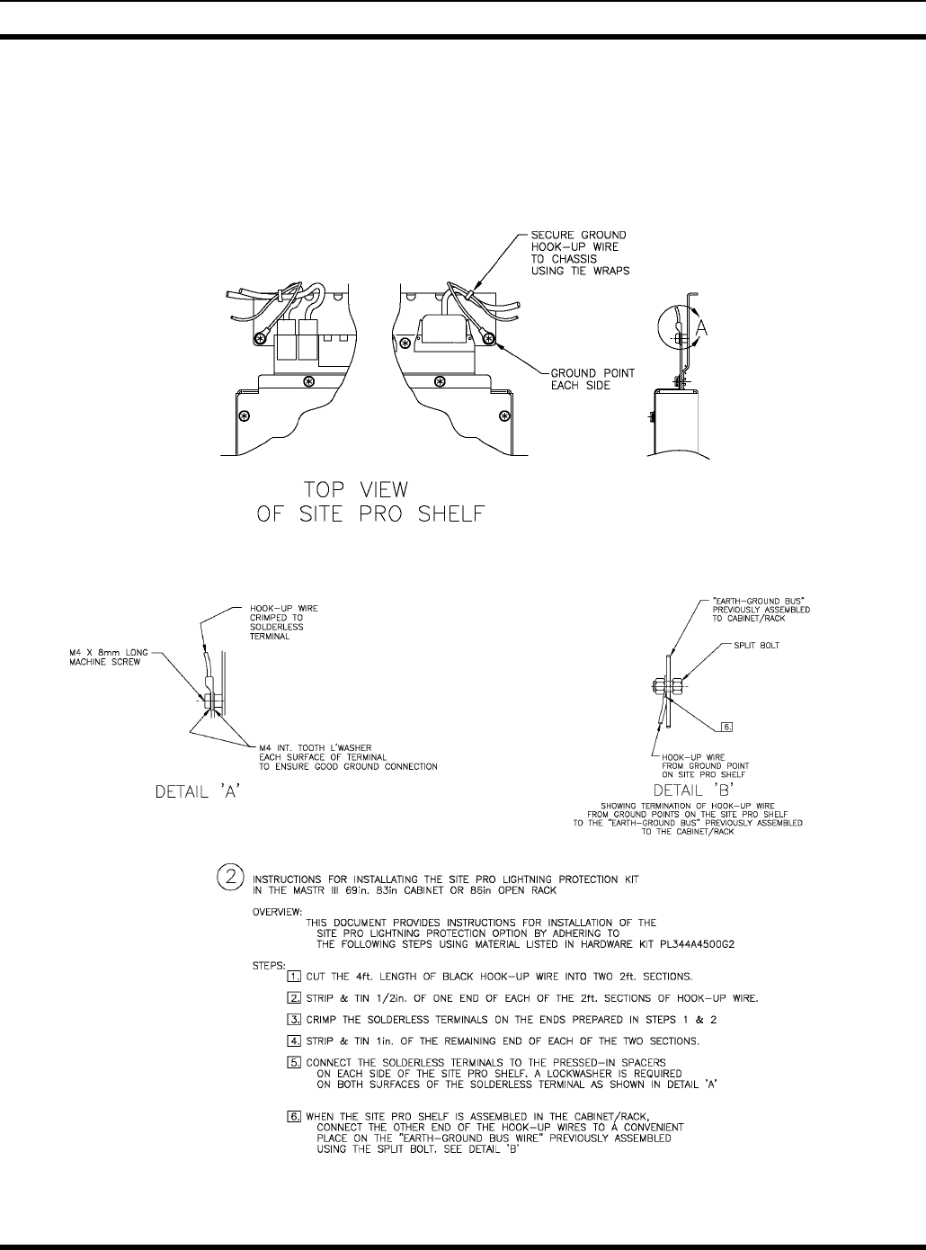
LIGHTNING PROTECTION GROUNDING
MM101271V1 R2A 85
10.0 LIGHTNING PROTECTION GROUNDING
Maximum lightning protection is achieved when the SitePro Lightning-Protection
Grounding Kit 344A4500G2 is installed. This kit is normally installed at the factory for
all trunking applications. The following procedure summarizes the installation process.
Continued
LIGNTNING PROTECTION GROUNDING
86 MM101271V1 R2A
NOTE
In order to be effective, the Cabinet Grounding Strap must be strapped to the building
and/or earth ground.
LIGHTING PROTECTION KIT 344A4500G2
ITEM
NUMBER
PART NUMBER DESCRIPTION
1
2
3 19B209260P1 Terminals: Solderless
4
5 19A116850P10 Wire: Stranded
6 344A4060P1 Connector: Split Bolt
7
8 19A700032P7 Washer: M4 Internal
Tooth
9 19A702364P508 Screw, M4 x 8
10 19J706152P5 Strap: Retention

PARTS LIST
MM101271V1 R2A 87
11.0 PARTS LIST
SitePro Controller SHELF ASSEMBLY
EA101209V1
SYMBOL PART NUMBER DESCRIPTION
1 MA101080V1 Chassis Assembly.
2 19A116552P3 Clamp, Cable.
3 FM101081V1 Cover.
4 19A702381P608 Screw, Thread Form, TORX, M4 x 8mm.
5 19A701312P6 Flat washer, M4.
6 19A702364P508 Screw, Machine, TORX, M4X8mm.
7 19A700032P7 Lock washer, Internal Tooth, M4.
8 FM101231V1 Spacer Plate, Shelf Door.
9FM101232V1 Lens keeper, Door.
10 AG101229V22 EMI Shielding Gasket, 22 Fingers.
11 AG101229V5 EMI Shielding Gasket, 5 Fingers.
12 AG101230V1 Lens, EMI Shielding.
13 19A700032P3 Lock washer, Internal Tooth, M2.5.
14 19A700034P3 Nut, M2.5 X 0.45.
15 NP101233V1 Rear Label.
16 FM101083V1 Support, Front.
A1 CB101073V1 INTERCONNECT BOARD
- - - - CAPACITORS - - - -
C1
and
C2
470pF, 2KV: sim to Arco MC1808X471KN202.
- - - - JACKS - - - -
J1
thru
J3
DIN 96_ABC-P: sim to AMP 650895-4.
J4 RJ11_MULT (2 x 2): sim Stewart SS-7368H22-NF.
J5
thru
J6
CON10: sim to Stewart SS-7188S-A-NF.
J7 19A116659P173 CONN PWR 4-R.
J8 19A116659P101 CONN PWR 3-P: sim to Molex 26-60-5030.
J9 19A116659P105 CONN RCPT 6: sim to Molex 26-60-5060.
J10 19A704852P30 CONN RCPT 4.
J11 HEADER 20: sim to AMP 102160-4.
J12 CON24: sim to AMP 102160-5.
J13 HEADER 26: sim to AMP 102160-6.
J14 RJ45_MULT ((2 x 6): sim to Stewart SS-73100-070.
PARTS LIST
88 MM101271V1 R2A
SYMBOL PART NUMBER DESCRIPTION
- - - - RESISTORS - - - -
R1
thru
R4
REP_623_642/75 75 Ohms, 1%, 0.63W.
- - - - TEST POINTS - - - -
TP3
thru
TP7
Test Points: sim to Component Corp. TP-107-01.
- - - - Pi FILTERS - - - -
U1
thru
U29
Capacitor: 100pF, 100WVDC@125º C, +80%/-20%:
sim to Tusonix 4700 006.
A2 CB101069V1 CONTROLLER BOARD
- - - - BATTERY - - - -
BT1 Coin: 3V. 165 mAh: Sim to Panasonic BR2325-1HM
or RAYOVAC BR2325T2.
- - - - CAPACITORS - - - -
C1 RJE584320/1 Tantalum: 1.0µF, 20V ±20%.
C2
thru
C11
19A702052P33 Ceramic: 0.1µF, 25V ±10%.
C12 RJE584320/1 Tantalum: 1.0µF, 20V ±20%.
C13 19A702052P33 Ceramic: 0.1µF, 25V ±10%.
C14 Ceramic: 470pF, 2kV ±20%: sim to MURATA
GRM432X7R471KAL.
C15
thru
C30
19A702052P33 Ceramic: 0.1µF, 25V ±10%.
C31 Ceramic: 470pF, 2kV ±20%: sim to MURATA
GRM432X7R471KAL.
C32
thru
C38
19A702052P33 Ceramic: 0.1µF, 25V ±10%.
C39 RJE584320/1 Tantalum: 1.0µF, 20V ±20%.
C40
and
C41
19A702052P33 Ceramic: 0.1µF, 25V ±10%.
C42 RJE584320/1 Tantalum: 1.0µF, 20V ±20%.

PARTS LIST
MM101271V1 R2A 89
SYMBOL PART NUMBER DESCRIPTION
C43
thru
C45
19A702052P33 Ceramic: 0.1µF, 25V ±10%.
C46 RJE584320/1 Tantalum: 1.0µF, 20V ±20%.
C47
and
C48
19A702052P33 Ceramic: 0.1µF, 25V ±10%.
C49 19A702061P13 Ceramic: 10pF, 100V ±10%.
C50
thru
C56
19A702052P33 Ceramic: 0.1µF, 25V ±10%.
C57 RJE5843208/1 Tantalum: 10µF, 16V±20%.
C58
thru
C62
19A702052P33 Ceramic: 0.1µF, 25V ±10%.
C63 19A702061P13 Ceramic: 10pF, 100V ±10%.
C64 19A702052P33 Ceramic: 0.1µF, 25V ±10%.
C65 19A702061P61 Ceramic: 100pF, 100V±10%.
C66 19A702061P57 82pF
C67 19A702052P33 Ceramic: 0.1µF, 25V ±10%.
C68 RJC4643033/82 Ceramic: 820pF, 25V±10%.
C69
thru
C73
19A702052P33 Ceramic: 0.1µF, 25V ±10%.
C74 RJE584320/1 Tantalum: 1.0µF, 20V ±20%.
C75
thru
C92
19A702052P33 Ceramic: 0.1µF, 25V ±10%.
C93 RJC4643034/1 Ceramic: 0.001µF, 25V ±10%.
C94
thru
C95
19A702052P33 Ceramic: 0.1µF, 25V ±10%.
C96
and
C97
RJE5843208/1 Tantalum: 10µF, 16V±20%.
C98
and
C99
19A702052P33 Ceramic: 0.1µF, 25V ±10%.
C100 RJE584320/1 Tantalum: 1.0µF, 20V ±20%.
C101
thru
C105
19A702052P33 Ceramic: 0.1µF, 25V ±10%.
C106 RJC4643034/1 Ceramic: 0.001µF, 25V ±10%.

PARTS LIST
90 MM101271V1 R2A
SYMBOL PART NUMBER DESCRIPTION
C107
thru
C110
19A702052P33 Ceramic: 0.1µF, 25V ±10%.
C111 RJC4643034/1 Ceramic: 0.001µF, 25V ±10%.
C112
thru
C114
19A702052P33 Ceramic: 0.1µF, 25V ±10%.
C115 19A702052P37 Ceramic: 0.033µF, 25V ±10%.
C116 19A702052P33 Ceramic: 0.1µF, 25V ±10%.
C117 Tantalum: 10 µF, 16V, low profile, ±20%: sim to AVX
TAJT106M010.
C118
thru
C120
19A702052P33 Ceramic: 0.1µF, 25V ±10%.
- - - - DIODES - - - -
D1
thru
D4
LED: Red, Thru-hole, RT ANGLE: sim to
HLMP1301-A1.
D5 LED: Green, Thru-hole, RT ANGLE: sim to
HLMP1503-A1.
D6
and
D7
LED: Yellow, sim to Citizen 1206: sim to Citizen CL-
150Y.
D8 LED: Green, Thru-hole, RT ANGLE: sim to
HLMP1503-A1.
D9
and
D10
LED: Yellow, sim to Citizen 1206: sim to Citizen CL-
150Y.
D11 Dual, High-Speed: sim to Philips, BAV99, SOT23.
D12 LED: Green, thru-hole: sim to Citizen CL-150G.
D13
thru
D29
Dual, High-speed: sim to Philips, BAV99, SOT23.
D32
and
D33
Dual, High-speed: sim to Philips, BAV99, SOT23.
- - - - JACKS - - - -
J1 Header 5x2: sim to AMP 146130-4.
J2 Header 22x2: sim to Samtec ASP-67352-01.
J3 MICTOR-38 Pin: sim to AMP 2-767004-2 (Not
placed).
J4 Header 4x2: sim to AMP 87227-4 (Not placed).
J5
and
J6
MICTOR-38 Pin: sim to AMP 2-767004-2 (Not
placed).

PARTS LIST
MM101271V1 R2A 91
SYMBOL PART NUMBER DESCRIPTION
J7 DIN96, 32x3, 0.1x0.1 Header: sim to Burndy
P196B80P00F0NN9.
J8 Telephone jack RJ-11, Rt Angle, non-shielded: sim to
AMP 555163-1.
J9 Header 22x2: sim to Samtec ASP-67352-01.
J10 Header 5x2: sim to AMP 146130-4.
- - - - INDUCTOR - - - -
L1 39µH ±15%: sim to Panasonic ELJ-FA390JF.
- - - - RESISTORS - - - -
R1 19A149818P103 Metal Film: 10k Ohms ±5%, 0.1W.
R2
thru
R4
19A149818P102 Metal Film: 1k Ohms ±5%, 0.1W.
R5 19A149818P103 Metal Film: 10k Ohms ±5%, 0.1W.
R6
thru
R8
19A149818P040 Metal Film: 0 Ohms.
R9
thru
R13
19A149818P390 Metal Film: 39 Ohms.
R14
and
R15
19A149818P750 Metal Film: 75 Ohms ±5%, 0.1W.
R16
and
R17
19A149818P103 Metal Film: 10k Ohms ±5%, 0.1W.
R18 19A149818P040 Metal Film: 0 Ohms.
R19 19A149818P222 Metal Film: 2.2k Ohms ±5%, 0.1W.
R20
and
R21
19A149818P390 Metal Film: 39 Ohms
R22 REP623642/499 49.9 Ohms ±1%.
R23 19A149818P331 Metal Film: 330 Ohms ±5%, 0.1W.
R24 19A149818P152 Metal Film: 1.5k Ohms ±5%, 0.1W.
R25 19A149818P102 Metal Film: 1k Ohms ±5%, 0.1W.
R26
and
R27
19A149818P390 Metal Film: 39 Ohms.
R28
and
R29
19A149818P103 Metal Film: 10k Ohms ±5%, 0.1W.
R30
and
R31
19A149818P390 Metal Film: 39 Ohms.

PARTS LIST
92 MM101271V1 R2A
SYMBOL PART NUMBER DESCRIPTION
R32
thru
R34
REP623642/499 49.9 Ohms ±1%.
R35 19A149818P331 Metal Film: 330 Ohms ±5%, 0.1W.
R36
and
R37
19A149818P390 Metal Film: 39 Ohms.
R38 REP623645/1 10k Ohms ±1%
R39 19A149818P103 Metal Film: 10k Ohms ±5%, 0.1W.
R40
and
R41
19A149818P750 Metal Film: 75 Ohms ±5%, 0.1W.
R42 19A149818P331 Metal Film: 330 Ohms ±5%, 0.1W.
R43 (Not Placed)
R44 19A149818P103 Metal Film: 10k Ohms ±5%, 0.1W.
R45 (Not Placed)
R46
thru
R50
19A149818P103 Metal Film: 10k Ohms ±5%, 0.1W.
R51 19A149818P390 Metal Film: 39 Ohms
R52
and
R53
REP623642/499 49.9 Ohms ±1%.
R54 19A149818P331 Metal Film: 330 Ohms ±5%, 0.1W.
R55 19A149818P121 Metal Film: 120 Ohms ±5%, 0.1W.
R56
and
R57
19A149818P102 Metal Film: 1k Ohms ±5%, 0.1W.
R58 19A149818P103 Metal Film: 10k Ohms ±5%, 0.1W.
R59 19A149818P121 Metal Film: 120 Ohms ±5%, 0.1W.
R60 19A149818P102 Metal Film: 1k Ohms ±5%, 0.1W.
R61 19A149818P121 Metal Film: 120 Ohms ±5%, 0.1W.
R62
and
R63
19A149818P102 Metal Film: 1k Ohms ±5%, 0.1W.
R64
and
R65
REP623642/499 49.9 Ohms ±1%.
R66 19A149818P121 Metal Film: 120 Ohms ±5%, 0.1W.
R67 19A149818P103 Metal Film: 10k Ohms ±5%, 0.1W.
R68
and
R70
19A149818P102 Metal Film: 1k Ohms ±5%, 0.1W.

PARTS LIST
MM101271V1 R2A 93
SYMBOL PART NUMBER DESCRIPTION
R71
and
R72
19A149818P121 Metal Film: 120 Ohms ±5%, 0.1W.
R73
and
R74
19A149818P105 Metal Film: 1 Meg Ohm ±5%, 0.1W.
R75 3.01k Ohms ±1%: sim to ROHM MZR03EZHF3101.
R76 19A149818P102 Metal Film: 1k Ohms ±5%, 0.1W.
R77
thru
R79
19A149818P103 Metal Film: 10k Ohms ±5%, 0.1W.
R80 19A149818P333 Metal Film: 33k Ohms
R81 19A149818P102 Metal Film: 1k Ohms ±5%, 0.1W.
R82 19A149818P390 Metal Film: 39 Ohms.
R83 19A149818P102 Metal Film: 1k Ohms ±5%, 0.1W.
R84 19A149818P103 Metal Film: 10k Ohms ±5%, 0.1W.
R85 REP623645/1 10.0k Ohms ±1%.
R86 19A149818P103 Metal Film: 10k Ohms ±5%, 0.1W.
R87 19A149818P331 Metal Film: 330 Ohms ±5%, 0.1W.
R88 19A149818P103 Metal Film: 10k Ohms ±5%, 0.1W.
R89 19A149818P102 Metal Film: 1k Ohms ±5%, 0.1W.
R90 19A139818P106 Metal Film: 10 Meg Ohms ±5%, 1/16W.
R91
thru
R94
19A149818P103 Metal Film: 10k Ohms ±5%, 0.1W.
R95 REP623646/47 470k Ohms ±1%.
R96 19A149818P102 Metal Film: 1k Ohms ±5%, 0.1W.
R97 19A149818P390 Metal Film: 39 Ohms.
R98 19A149818P204 Metal Film: 200k Ohms.
R99 (Not Placed)
R100
thru
R110
19A149818P103 Metal Film: 10k Ohms ±5%, 0.1W.
R111 19A149818P750 Metal Film: 75 Ohms ±5%, 0.1W.
R112
thru
R122
19A149818P103 Metal Film: 10k Ohms ±5%, 0.1W.
R123 19A149818P390 Metal Film: 39 Ohms.
R124
thru
R135
19A149818P103 Metal Film: 10k Ohms ±5%, 0.1W.
R136 19A149818P222 Metal Film: 2.2k Ohms ±5%, 0.1W

PARTS LIST
94 MM101271V1 R2A
SYMBOL PART NUMBER DESCRIPTION
R137
thru
R139
19A149818P103 Metal Film: 10k Ohms ±5%, 0.1W.
R140
and
R141
19A149818P511 Metal Film: 510 Ohms.
R142
and
R143
19A149818P222 Metal Film: 2.2k Ohms ±5%, 0.1W.
R144 19A149818P103 Metal Film: 10k Ohms ±5%, 0.1W.
R145 19A149818P511 Metal Film: 510 Ohms.
R146 19A149818P103 Metal Film: 10k Ohms ±5%, 0.1W.
R147 19A149818P392 Metal Film: 3.9k Ohms.
R148 19A149818P103 Metal Film: 10k Ohms ±5%, 0.1W.
R149 19A149818P101 Metal Film: 100 Ohms.
R150 19A149818P392 Metal Film: 3.9k Ohms.
R151
and
R152
19A149818P511 Metal Film: 510 Ohms
R153 0.015 Ohms ±1%, 0.5W ±1%: sim to IRC-TT LRC-
LRF1206-01-R015-F.
R154 19A149818P511 Metal Film: 510 Ohms
R155
thru
R158
19A149818P103 Metal Film: 10k Ohms ±5%, 0.1W.
R159 19A149818P102 Metal Film: 1k Ohms ±5%, 0.1W.
R160 19A149818P392 Metal Film: 3.9k Ohms
R161 19A149818P100 Metal Film: 10 Ohms ±5%, 0.1W
R162 19A149818P101 Metal Film: 100 Ohms.
R163 19A149818P511 Metal Film: 510 Ohms.
R164
and
R165
19A149818P102 Metal Film: 1k Ohms ±5%, 0.1W.
R166 19A149818P511 Metal Film: 510 Ohms.
R167 REP623644/56 5.6k Ohms ±1%, 0.1W.
R168 REP623644/2 2.0k Ohms ±1%, 0.1W.
R169 19A149818P101 Metal Film: 100 Ohms.
R170 19A149818P392 Metal Film: 3.9k Ohms.
R171 19A149818P472 Metal Film: 4.7k Ohms ±5%. 0.1W.
R172 19A149818P273 Metal Film: 27k Ohms
R173 19A149818P222 Metal Film: 2.2k Ohms ±5%, 0.1W.
R174 Not Used

PARTS LIST
MM101271V1 R2A 95
SYMBOL PART NUMBER DESCRIPTION
R175
and
R176
19A149818P103 Metal Film: 10k Ohms ±5%, 0.1W.
R177 19A149818P472 Metal Film: 4.7k Ohms ±5%. 0.1W.
R178 19A149818P103 Metal Film: 10k Ohms ±5%, 0.1W.
R179 19A149818P472 Metal Film: 4.7k Ohms ±5%. 0.1W.
R180 19A149818P103 Metal Film: 10k Ohms ±5%, 0.1W.
R181 100k Ohms ±5%, 0.1W.
R182 Not Used
R183 19A149818P040 Metal Film: 0 Ohms.
R184
thru
R186
19A149818P103 Metal Film: 10k Ohms ±5%, 0.1W.
R187 19A149818P040 Metal Film: 0 Ohms
R188 19A149818P152 Metal Film: 1.5k Ohms ±5%, 0.1W.
R189 19A149818P102 Metal Film: 1k Ohms ±5%, 0.1W.
R190
and
R191
REP623644/56 5.6k Ohms ±1%, 0.1W.
R192 19A149818P333 Metal Film: 33k Ohms
R193 19A149818P390 Metal Film: 39 Ohms.
R194 (Not placed)
R195 19A149818P103 Metal Film: 10k Ohms ±5%, 0.1W.
R196
and
R197
19A149818P040 Metal Film: 0 Ohms
- - - - RESISTOR NETWORKS - - - -
RN1
thru
RN15
10k Ohms, BUS8, ±5%, 0.063W: sim to CTC
745C101103JTR.
- - - - SWITCHES - - - -
S1 PUSHBUTTON, SPST N.O./SPST N.C.: sim to
Grayhill 32-01.
S2 DIPSWITCH, 8 position: sim to Grayhill 97S08SR.
- - - - TEST POINTS - - - -
TP1
thru
TP10
SM Test Point Loop – Surface Mount: sim to ADI/
SM-TESTPAD/Components-Corporation TP-107-01.
- - - - TRANSFORMERS - - - -
T1
and
T2
1:1, 10/100Mbps: sim to TG110-S05N2.

PARTS LIST
96 MM101271V1 R2A
SYMBOL PART NUMBER DESCRIPTION
- - - - TRANSISTORS - - - -
Q1 NPN: Switching: sim to Phillips PMBT3904, SOT23.
Q2
thru
Q4
FET: Small-Signal, N-Channel: sim to INFINEON,
BSP295.
Q5 MOSFET: N-Channel, 5A, 20V: sim to ON
Semiconductor, MMSF5N02HD.
Q6
and
Q7
NPN: Switching: sim to Phillips PMBT3904, SOT23.
Q8 PNP: sim to Motorola, MMBT3906LT1, SOT23.
Q9
and
Q10
NPN: Switching: sim to Phillips PMBT3904, SOT23.
- - - - INTEGRATED CIRCUITS - - - -
U1 Single Buffer with 3-State Output: sim to Fairchild
NC7SZ125M5, SOT23-5.
U2 8M x 16 SDRAM, PC100: sim to Micron
MT48LC8M16A2TG-8E, TSOP54.
U3 Silicon Serial Number: sim to Dallas, DS2401P,
TSOC6.
U4 Clock Buffer: sim to Cypress Cy2305SC-1, SOIC8.
U5 10/100-TX/FX Ethernet Transceiver: sim to AMD
AM79C874VC, TQFP80.
U6 Octal Buffer, 3.3V: sim to TI 74LVC244ADB,
SSOP20.
U7 8M x 16 SDRAM, PC100: sim to Micron
MT48LC8M16A2TG-8E, TSOP54.
U8 Octal Buffer, 3.3V: sim to TI 74LVC244ADB, SOP20.
U9 Microprocessor, 66MHz: sim to Motorola,
XPC860PZP66D4, BGA357.
U10 SK101412V1 1M x 16/2M x 8 Flash, simultaneous Read/Write
(programmed): sim to AMD, AM29DL163DB90E1,
TSOP48 (unprogrammed).
U11 SK101412V2 1M x 16/2M x 8 Flash, simultaneous Read/Write
(programmed): sim to AMD, AM29DL163DB90E1,
TSOP48 (unprogrammed).
U12 10/100-TX/FX Ethernet Transceiver: sim to AMD
AM79C874VC, TQFP80.
U13 RS232 Transceiver, 5V, 2-TX, 2-RX: sim to MAXIM,
MAX202CSE, SOIC16.
U14 2-wire serial 128k (16k x 8) EEPROM, I2C, 3.3V: sim
to Atmel, AT24C128N-10SC-2.7, SOIC8.
U15 I2C Bus 8-bit I/O: sim to Philips, PCF8574T, SOIC16.

PARTS LIST
MM101271V1 R2A 97
SYMBOL PART NUMBER DESCRIPTION
U16 Phase-Lock-Loop (PLL): sim to TI, 74HCT4046ADB,
SSOP20.
U17 Single Inverter: sim to Philips, 74HC1G04GW, SOT-
353.
U18 HEX Buffer: sim to Philips, 74HC14PW, TSSOP14.
U19 Octal XCVR, BUS HOLD, 3.3V, sim to Philips,
74LVCH245APW, TSSOP20.
U20 Single Inverter: sim to Philips, 74HC1G04GW, SOT-
353.
U21 RS485 Transceiver: sim to TI, 75176BD, SO8.
U22
and
U23
HEX Buffer: sim to Philips, 74HC14PW, TSSOP14.
U24 RS232 Transceiver, 3V to 5.5V, 3-TX, 5-RX: sim to
MAXIM, MAX3241CAI, SSOP28.
U25 +5V Regulator, 1.5A: sim to Linear Tech, LT1086CM-
3.3, TO263.
U26 I2C Bus 8-bit I/O: sim to Philips, PCF8574T, SOIC16.
U27 MAX3000A 144 PIN EPLD, sim to Altera,
EPM3256ATC144-10, TQFP144.
U28 Quad UART (QUART): sim to SC28L194A1BE,
TQFP80.
U29 HEX Buffer: sim to Philips, 74HCT14PW, TSSOP14.
U30 RS232 Transceiver, 5V, 4-TX, 5-RX: sim to MAXIM,
MAX213CAI, SSOP28.
U31 Reset Supervisor: sim to Dallas, DS1818R-10,
SOT23.
U32 HEX Buffer: sim to Philips, 74HCT14PW, TSSOP14.
U33
thru
U35
HEX Open-Collector Output Drivers: sim to Philips,
7406AD, SOIC14.
U36 RS232 Transceiver, 3V to 5.5V, 5-TX, 3-RX: sim to
MAXIM, MAX3237CAI, SSOP28.
U37 Hot Swap Controller: sim to Linear Tech, LTC1422,
SOCI8.
U38 Single 2-Input NAND Gate: sim to Phillips,
74AHC1G00GW, SOT353.
U39 Not Used
U40 555 Timer: sim to National, LMC555CM, TO263.
U41
and
U42
Single Inverter: sim to Phillips 74AC1G04GW.
U43 REAL TIME CLOCK, IND.: sim to Dallas DS1307ZN.

PARTS LIST
98 MM101271V1 R2A
SYMBOL PART NUMBER DESCRIPTION
- - - - OSCILLATORS - - - -
Y1 Crystal: 25MHz CLK ±50ppm, 40%/60% duty, 3.3V:
sim to Raltron CO4305-25.0000-TR
Y2 Crystal: 29.4912 MHz CLK ±100ppm, 40%/60%
duty, 3.3V: sim to Raltron CO4310-29.4912-TR.
Y3 Crystal: 32.786kHz CLK: sim to Raltron RSE-32.768-
12.5-H2.
Y4 Crystal: 11.0592 MHz CLK ±50ppm, 40%/60% duty,
3.3V: sim to Raltron CO4305-11.0592-TR..
Y5 Crystal: 32.786kHz CLK: sim to Raltron RSE-32.768-
12.5-H2.
A2-A1 CB101074V1 SitePro MODEM BOARD
- - - - CAPACITORS - - - -
C1
thru
C2
RJE 584 3208/1 Tantalum: 10µF
C3
thru
C27
RJC 464 3046/1 Ceramic: 0.1µF
- - - - CONNECTORS - - - -
J1
and
J2
I/O: QUICC, Edge 22x2: sim to Samtec
CLP-122-02-G-D-BE
J3 Diagnostic Connector: sim to Semtec FTSH-110-01-
L-DV.
- - - - RESISTORS - - - -
R1
thru
R8
REP 622 455/1 10k Ohms ±5%, 0.06W.
R9 Not Used.
R10 REP 622 455/1 10k Ohms ±5%, 0.06W.
R11
thru
R13
REP 622 454/1 1k Ohms ±5%, 0.06W.
R14 REP 622 453/27 270 Ohms ±5%, 0.06W.
R15
thru
R20
REP 622 455/1 10k Ohms ±5%, 0.06W.
- - - - INTEGRATED CIRCUITS - - - -
U1 Local Microprocessor (socketed): sim to Dallas
DS80C323QCD.
U2 SRAM 64 x 8k: sim to Integrated Circuit Devices
IDT71V124SA20PH.
U3 Dual Port RAM: sim to Integrated Circuit Devices
IDT70V05L55PF.

PARTS LIST
MM101271V1 R2A 99
SYMBOL PART NUMBER DESCRIPTION
U4 SRAM 64 x 8k: sim to Integrated Circuit Devices
IDT71V124SA20PH.
U5 Address Decoder: sim to 74LVC138ADB.
U6 3.3V - 5V Converter: sim to Integrated Circuit
Devices IDT74FCT164245TPA.
U7 8-Bit Latch: sim to Philips 74LVC373APWDH.
U8 Not Used.
U9
thru
U11
ROP 101 688/4C RF/PL/VDI Modem
U12 Adder Bus Buffer: sim to Integrated Circuit Devices
IDT74FCT163245APF.
U13 Data Bus Buffer: sim to Integrated Circuit Devices
IDT74FCT3245APG
U14
and
U15
Not Used.
U16 Quad 3-Input NAND Gate: sim to Philips
74LVC10APWDH.
U17 Quad 2-Input NOR Gate: sim to Philips
74LVC02APWDH.
U18 Hex Inverter: sim to Philips 74LVC04APWDH.
U19 Quad 2-Input NAND Gate: sim to Philips
74HC1G00GW.
U20
thru
U22
Single Inverter: sim to Philips 74HC1G04GW.
U23 Quad 2-Input NAND Gate: sim to Philips
74HC1G00GW.
U24
and
U25
Single Inverter: sim to Philips 74HC1G04GW.
- - - - SOCKET - - - -
XU1 RNK 860 12/044 PLCC44
- - - - CABLES - - - -
W1 CA101211V1 Input To Power Supply.
W2 CA101212V1 Output From Power Supply.
C87
and
C88
Not Used.
C89
thru
C91
0.1µF: sim to Panasonic ECJ-1VB1C104K
C92 Not Used.

PARTS LIST
100 MM101271V1 R2A
SYMBOL PART NUMBER DESCRIPTION
C93
thru
C98
0.1µF: sim to Panasonic ECJ-1VB1C104K
C100
thru
C104
0.1µF: sim to Panasonic ECJ-1VB1C104K
C106
thru
C111
0.1µF: sim to Panasonic ECJ-1VB1C104K
C112 Not Used
C113
thru
C121
0.1µF: sim to Panasonic ECJ-1VB1C104K
C123 4.7pF: sim to Kemet C0603C479K5GAC
C124
and
C125
0.1µF: sim to Panasonic ECJ-1VB1C104K
- - - - DIODES - - - -
D1
and
D2
: sim to Motorola BAT54LT1
D3
and
D4
Not Used.
D5 Dual High Speed: sim to Philips Semiconductors
BAL99.
D6
thru
D9
: sim to Motorola BAT54LT1.
D10 Not Used.
D11
and
D12
Dual High Speed: sim to Philips Semiconductors
BAL99.
D13
and
D14
Not Used.
D15 : sim to Motorola BAT54LT1.
- - - - JACK - - - -
J1 DIN96_ABC_R: sim to AMP 536366-5.
- - - - RELAYS - - - -
K1
and
K2
2FORMC: sim to NEC EB2-4.5S.
- - - - TRANSISTOR - - - -
Q1 NPN: Switching: sim to Motorola MMBT3904LT1.

PARTS LIST
MM101271V1 R2A 101
SYMBOL PART NUMBER DESCRIPTION
- - - - RESISTORS - - - -
R1 124k Ohms: sim to Panasonic ERJ-3EKF1243V.
R2 Resistor network: SM/RP_EXB-D10C [EXB-
D10C/SM]: sim to Panasonic EXB-D10C103J.
R3 Not Used.
R4 16k Ohms: sim to Panasonic ERJ-3EKF1602V.
R5 1.21k Ohms: sim to Panasonic ERJ-3EKF1211V.
R6 5.11k Ohms: sim to Panasonic ERJ-3EKF5111V.
R7 1k Ohms: sim to Panasonic ERJ-3EKF1001V.
R8 16k Ohms: sim to Panasonic ERJ-3EKF1602V.
R9 1.21k Ohms: sim to Panasonic ERJ-3EKF1211V.
R10 5.11k Ohms: sim to Panasonic ERJ-3EKF5111V.
R11 1k Ohms: sim to Panasonic ERJ-3EKF1001V.
R12
and
R13
Not Used.
R14 31.6k Ohms: sim to Panasonic ERJ-3EKF3162V.
R15 0 Ohms: sim to Panasonic ERJ-3EKF0.0V.
R16 150k Ohms: sim to Panasonic ERJ-3EKF1503V.
R17 100k Ohms: sim to Panasonic ERJ-3EKF1003V.
R18 1Meg Ohm: sim to Panasonic ERJ-3EKF1004V.
R19 Not Used.
R20 1Meg Ohms: sim to Panasonic ERJ-3EKF1004V.
R21 0 Ohms: sim to Panasonic ERJ-3EKF0.0V.
R22 100k Ohms: sim to Panasonic ERJ-3EKF1003V.
R23
and
R24
Not Used.
R25 46.4k Ohms: sim to Panasonic ERJ-3EKF4642V.
R26 0 Ohms: sim to Panasonic ERJ-3EKF0.0V.
R27 100k Ohms: sim to Panasonic ERJ-3EKF1003V.
R28 11k Ohms: sim to Panasonic ERJ-3EKF1102V.
R29 1.96k Ohms: sim to Panasonic ERJ-3EKF1961V.
R30 5.11k Ohms: sim to Panasonic ERJ-3EKF5111V.
R31 1.1k Ohms: sim to Panasonic ERJ-3EKF1101V.
R32 11k Ohms: sim to Panasonic ERJ-3EKF1102V.
R33 1.96k Ohms: sim to Panasonic ERJ-3EKF1961V.
R34 5.11k Ohms: sim to Panasonic ERJ-3EKF5111V.
R35 1.1k Ohms: sim to Panasonic ERJ-3EKF1101V.
R36 470 Ohms: sim to Panasonic ERJ-3EKF4700V.

PARTS LIST
102 MM101271V1 R2A
SYMBOL PART NUMBER DESCRIPTION
R37
and
R38
1Meg Ohms: sim to Panasonic ERJ-3EKF1002V.
R39 22.1k Ohms: sim to Panasonic ERJ-3EKF2212V.
R40 20K Ohms: sim to Panasonic ERJ-3EKF2002V.
R41 22.1k Ohms: sim to Panasonic ERJ-3EKF2212V.
R42 Not Used.
R43 294k Ohms: sim to Panasonic ERJ-3EKF2943V.
R44
and
R45
22.1k Ohms: sim to Panasonic ERJ-3EKF2212V.
R46 10k Ohms: sim to Panasonic ERJ-3EKF1002V.
R47 10Meg Ohms: sim to Panasonic ERJ-3EKF1005V.
R48 Not Used.
R49 10k Ohms: sim to Panasonic ERJ-3EKF1002V.
R50 68k Ohms: sim to Panasonic ERJ-3EKF6802V.
R51 Not Used.
R52 100k Ohms: sim to Panasonic ERJ-3EKF1003V.
R53 10k Ohms: sim to Panasonic ERJ-3EKF1002V.
R54 0 Ohms: sim to Panasonic ERJ-3EKF0.0V.
R55 23.7k Ohms: sim to Panasonic ERJ-3EKF2372V.
R56
and
R57
Not Used.
R58 47k Ohms: sim to Panasonic ERJ-3EKF4702V.
R59
and
R60
10k Ohms: sim to Panasonic ERJ-3EKF1002V.
R61
and
R62
0 Ohms: sim to Panasonic ERJ-3EKF0.0V.
R63 20k Ohms: sim to Panasonic ERJ-3EKF2002V.
R64 Not Used.
R65 60.4k Ohms: sim to Panasonic ERJ-3EKF6042V
R66 Not Used.
R67 1k Ohms: sim to Panasonic ERJ-3EKF1001V.
R68 4.7k Ohms: sim to Panasonic ERJ-3EKF4701V.
R69 0 Ohms: sim to Panasonic ERJ-3EKF0.0V.
R70 60.4k Ohms: sim to Panasonic ERJ-3EKF6042V.
R71 Not Used.
R72
thru
R74
22.1k Ohms: sim to Panasonic ERJ-3EKF2212V.

PARTS LIST
MM101271V1 R2A 103
SYMBOL PART NUMBER DESCRIPTION
R75
thru
R77
Not Used.
R78
and
R79
10k Ohms: sim to Panasonic ERJ-3EKF1002V.
R80
thru
R83
Not Used.
R84 0 Ohms: sim to Panasonic ERJ-3EKF0.0V.
R85 Not Used.
R86 10k Ohms: sim to Panasonic ERJ-3EKF1002V.
R87 18k Ohms: sim to Panasonic ERJ-3EKF1802V.
R88 0 Ohms: sim to Panasonic ERJ-3EKF0.0V
R89 32.4k Ohms: sim to Panasonic ERJ-3EKF3242V.
R90 Not Used.
R91 82.5k Ohms: sim to Panasonic ERJ-3EKF8252V.
R92 Not Used.
R93
and
R94
Not Used.
R95 221k Ohms: sim to Panasonic ERJ-3EKF2213V.
R96 Not Used.
R97 10k Ohms: sim to Panasonic ERJ-3EKF1002V.
R98 82.5k Ohms: sim to Panasonic ERJ-3EKF8252V.
R99 10k Ohms: sim to Panasonic ERJ-3EKF1002V.
R100
thru
R102
Not Used.
R103
and
R104
4.7k Ohms: sim to Panasonic ERJ-3EKF4701V.
R105
thru
R108
470 Ohms: sim to Panasonic ERJ-3EKF4700V.
R109
and
R111
Not Used.
R112 4.7k Ohms: sim to Panasonic ERJ-3EKF4701V.
R113 10 Ohms ERJ-3EKF10R0V.
R114 0 Ohms ERJ-3EKF0.0V
R115
thru
R118
Not Used.

PARTS LIST
104 MM101271V1 R2A
SYMBOL PART NUMBER DESCRIPTION
R119
and
R120
0 Ohms: sim to Panasonic ERJ-3EKF0.0V.
R121 20k Ohms: sim to Panasonic ERJ-3EKF2002V.
R122 39.2k Ohms: sim to Panasonic ERJ-3EKF3922V.
R123
and
R124
51.1K Ohms: sim to Panasonic ERJ-3EKF5112V.
R125 39.2k Ohms: sim to Panasonic ERJ-3EKF3922V.
R126 332k Ohms: sim to Panasonic ERJ-3EKF3323V.
R127 Resistor network: sim to Panasonic EXB-D10C103J.
R128
thru
R130
0 Ohms: sim to Panasonic ERJ-3EKF0.0V.
R131 10Meg Ohms: sim to Panasonic ERJ-3EKF1005V.
R132
thru
R151
Not Used.
R152 100k Ohms: sim to Panasonic ERJ-3EKF1003V.
R153 10k Ohms: sim to Panasonic ERJ-3EKF1002V.
- - - - TEST POINTS - - - -
TP32
and
TP33
T POINT R: sim to Components Corp. TP-107-01.
- - - - INTEGRATED CIRCUITS - - - -
U2 Three-terminal negative fixed voltage (-5V) regulator:
sim to Motorola/On Semiconductors, MC79M05BT.
U3 Dual 4-Stage Binary Ripple Counter: sim to Motorola,
MC74HC393AD.
U4 Remote 16-bit I/O Expander: sim to Philips,
PCF8575CTS.
U5 High slew rate, wide bandwidth, single supply
operational amplifier: sim to Motorola/On
Semiconductors, MC33074D.
U6 High slew rate, wide bandwidth, single supply
operational amplifier: sim to Motorola/On
Semiconductors: sim to Motorola, MC33072D.
U7 Fault-Protected, High-Voltage Single 8-to-1/Dual 4-
to-1 Multiplexers: sim to Maxim, MAX4508ESE.
U8 Addressable dual digital potentiometer: sim to Dallas,
DS1803Z-010.
U9 SPST/SPDT Analog Switches: sim to Maxim,
DG419DY.

PARTS LIST
MM101271V1 R2A 105
SYMBOL PART NUMBER DESCRIPTION
U10 High slew rate, wide bandwidth, single supply
operational amplifier: sim to Motorola/On
Semiconductors: sim to Motorola,: sim to Motorola,
MC33074D
U11 8th-Order, Low-pass, Switched-Capacitor Filters: sim
to Maxim, MAX292ESA.
U12 Low power dual voltage comparator: sim to Motorola,
LM393D.
U13 Not Used.
U14 8th-Order, Lowpass, Elliptic, Switched-Capacitor
Filters: sim to Maxim, MAX294EWE.
U15 High slew rate, wide bandwidth, single supply
operational amplifier: sim to Motorola/On
Semiconductors: sim to Motorola, MC33072D.
U16 Quad Low Power RS-232 Driver: sim to Linear Tech,
LTC1067IS.
U17 High slew rate, wide bandwidth, single supply
operational amplifier: sim to Motorola/On
Semiconductors: sim to Motorola, MC33072D.
U18 SPST/SPDT Analog Switches: sim to Maxim,
DG419DY.
U19 High slew rate, wide bandwidth, single supply
operational amplifier: sim to Motorola/On
Semiconductors: sim to Motorola, MC33072D.
U20 Low Pass Filter: sim to Maxim, MAX294EWE.
U21 Not Used.
U22 SPST/SPDT Analog Switches: sim to Maxim,
DG419DY.
U23 8-Bit A/D and D/A Converter: sim to Philips,
PCF8591TD.
U24 +5V-Powered, Multi-channel RS-232
Drivers/Receivers: sim to Maxim, MAX232AESE.
U25 Quad Low Power RS-232 Driver: sim to Linear Tech,
LTC4861S.
U26 Quad RS-485 Line Receiver: sim to Linear Tech, LTC
489IS.
U27 Dual Peripheral Drivers: sim to TI, SN75451BD
U28 High slew rate, wide bandwidth, single supply
operational amplifier: sim to Motorola/On
Semiconductors: sim to Motorola, MC33072D.
U29
and
U30
Not Used
U31 Fault-protected, high-voltage, Single 4-to-1/Dual 2-to-
1 Multiplexers: sim to Maxim MAX4534ESD.

PARTS LIST
106 MM101271V1 R2A
SYMBOL PART NUMBER DESCRIPTION
U32 Hex Inverter: sim to Motorola MC14069UBDR2
U33 Low offset voltage dual comparators: sim to Motorola
LM393D.
U34 2-wire serial 128k (16k x 8) EEPROM, I2C, 3.3V: sim
to Atmel, AT24C128N-10SC-2.7, SOIC8.
- - - - CRYSTAL - - - -
Y1 400 kHz: sim to STATEK_CX-3V-SM
A5 PS-PS101328V1 POWER SUPPLY
+5.1V, +12V, -12V: sim to CONDOR DP1719
A6 EA101227V1 DISPLAY MODULE
1 FM101082V1 Display Cover
2 FM101082V2 Spacer Plate.
3 AG101230V1 Display Lens.
4 FM101082V3 Display Lens Keeper.
AR-FM101082V1 Display Mkg Artwork.
A6-A1 CB101077V1 Display Board Assembly
- - - - CAPACITORS - - - -
C1 0.1µF: sim to Panasonic ECJ-1VB1C104K.
C2 0.01µF: sim to Panasonic ECJ-1VB1C103K.
C3 22µF: sim to Sprague 293D226X9016D2T.
C4 0.01µF: sim to Panasonic ECJ-1VB1C103K.
C5 0.1µF: sim to Panasonic ECJ-1VB1C104K.
- - - - DIODE - - - -
D1 POWER ON: sim to LUMEX SSS-LX5093GD-0.150”.
- - - - RESISTORS - - - -
R1 300 Ohms: sim to Panasonic ERJ-6ENF3010.
R2
thru
R17
10k Ohms: sim to Panasonic ERJ-3EKF1002.
R18 19.6k Ohms: sim to Panasonic 3EKF1962.
R19
thru
R21
0 Ohms: sim to PHYCOMP 9C06031AOR00JLHFT.
R22 300 Ohms: sim to Panasonic ERJ-6ENF3010.
- - - - INTEGRATED CIRCUITS - - - -
U1 8-Character smart display: sim to SIEMENS
HDSP2112S.
U2 Remote 16-bit I/O expander for I2C-bus: sim to
Philips PCF8575TS.
A6-W1 CA101222V1 Cable
A7 RYTUZ 921 01/1 ROCKWELL MODEM ASSEMBLY
IC DATA
MM101271V1 R2A 107
12.0 IC DATA
12.1 CONTROLLER BOARD (A2)
U1
Single Buffer with 3-State Output
Fairchild, NC7SZ125M5, SOT23-5
U2, U7
8M x 16 SDRAM, PC100
Micron MT48LC8M16A2TG-8E
Continued on next page
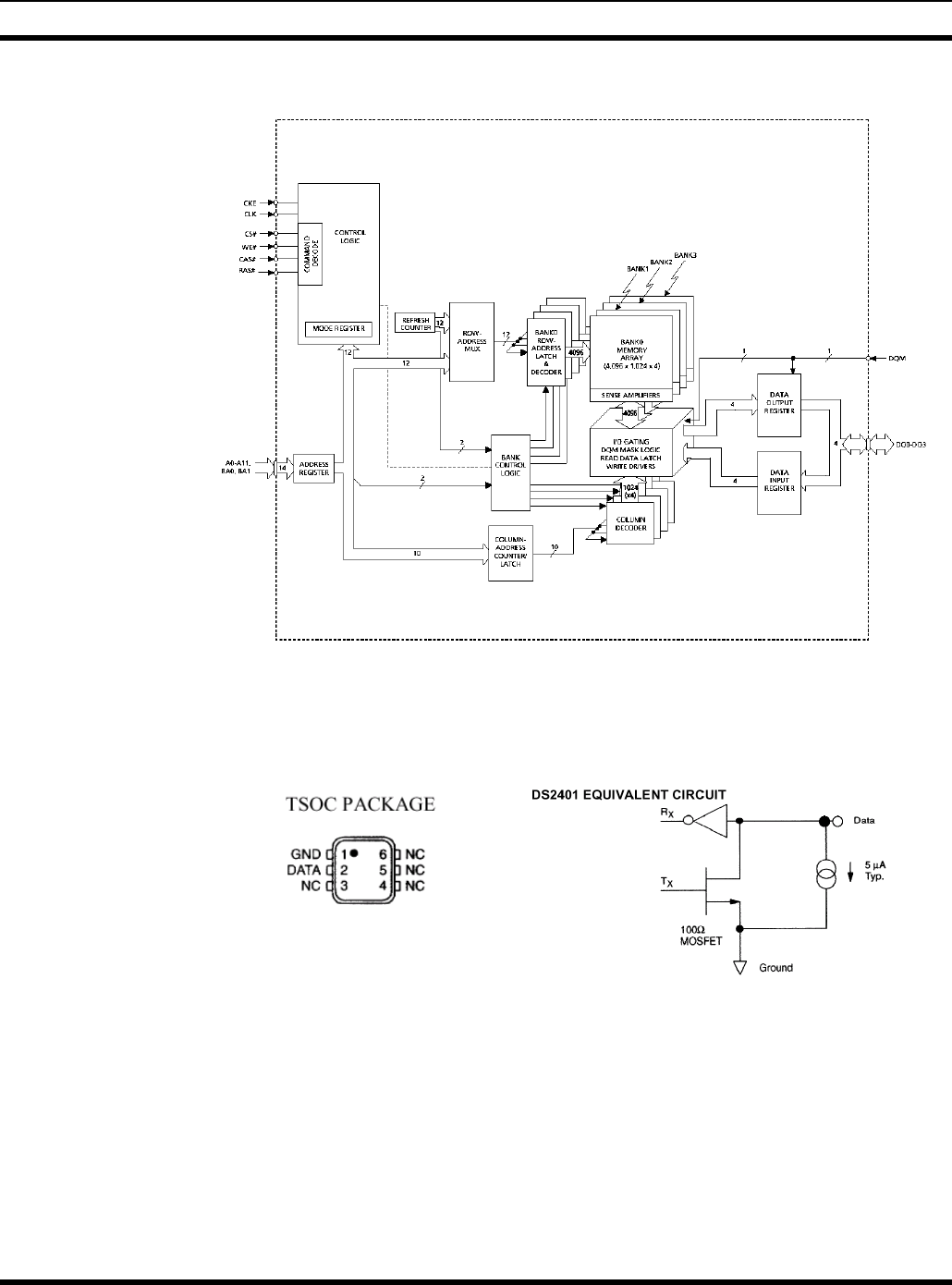
IC DATA
108 M101271V1 R2A
Continued from previous page
U3
Silicon Serial Number
DALLAS DS2401P
IC DATA
MM101271V1 R2A 109
U4
Clock Buffer
Cypress CY2305SC-1
U5, U12
10/100-TX/RX Ethernet Transceiver
AMD AM79C874VC
Continued on next page
IC DATA
110 M101271V1 R2A
Continued from pervious page
U6, U8
Octal Buffer, 3.3V
TI, 74LVC244ADB
IC DATA
MM101271V1 R2A 111
U9
Microprocessor, 66MHz
Motorola, XPC860PZP66D4, BGA357
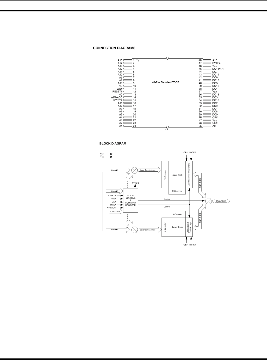
IC DATA
112 MM101271V1 R2A
U10, U11
1M x 16/2M x 8 Flash, Simultaneous Read/Write
AMD, AM29DL163DB90E1
IC DATA
MM101271V1 R2A 113
U13
RS232 Transceiver, 5V, 2-TX, 2-RX
MAXIM, MAX202CSE
U14
EEPROM, I2C, 16k x 8, 3.3V
Atmel, AT24C128N, SOIC8
IC DATA
114 MM101271V1 R2A
U15, U26
I2C Bus 8-Bit I/O
Philips, PCF8574A
PIN IDENTIFICATION
SYMBOL PIN DESCRIPTION
A0 1 Address Input 0
A1 2 Address Input 1
A2 3 Address Input 2
P0 4 Quasi-bidrectional I/O 0
P1 5 Quasi-bidrectional I/O 1
P2 6 Quasi-bidrectional I/O 2
P3 7 Quasi-bidrectional I/O 3
Vss 8 Supply Ground
P4 9 Quasi-bidrectional I/O 4
P5 10 Quasi-bidrectional I/O 5
P6 11 Quasi-bidrectional I/O 6
P7 12 Quasi-bidrectional I/O 7
INT 13 Interrupt Output (Active LOW)
SCL 14 Serial Clock Line
SDA 15 Serial Data Line
VDD 16 Supply Voltage
IC DATA
MM101271V1 R2A 115
U16
Phase-Lock-Loop (PLL)
TI, 74HCT4046ADB
U17, U20
Single Inverter
Philips, 74HC1G04GW
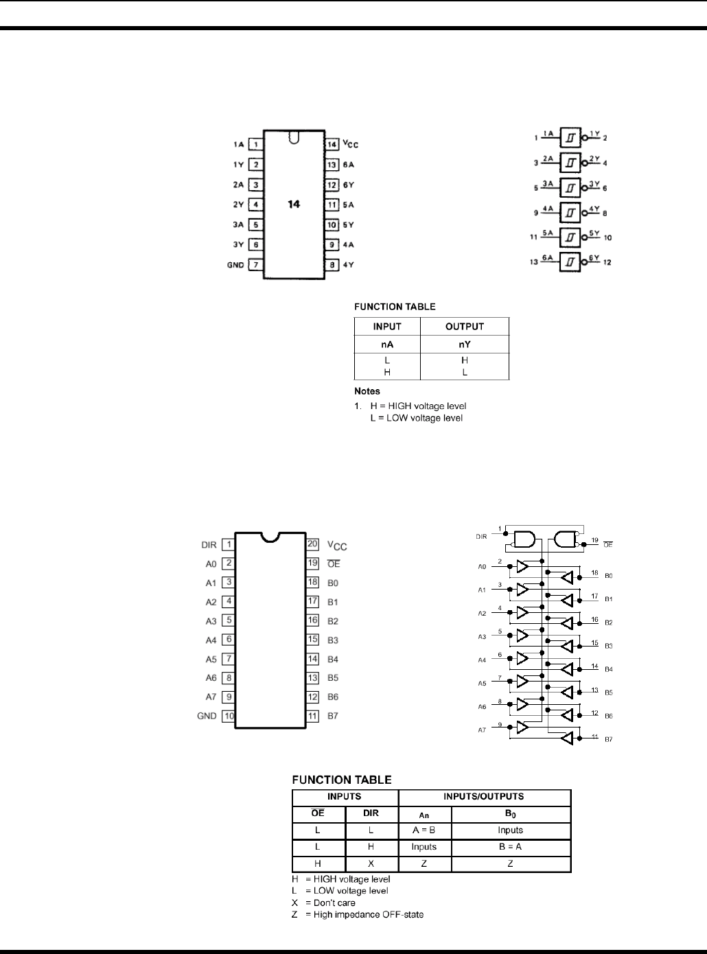
IC DATA
116 MM101271V1 R2A
U18, U22, U23
HEX Buffer
Philips, 74HC14PW
U19
Octal XCVR, BUS HOLD, 3.3V
Philips, 74LVCH245APW
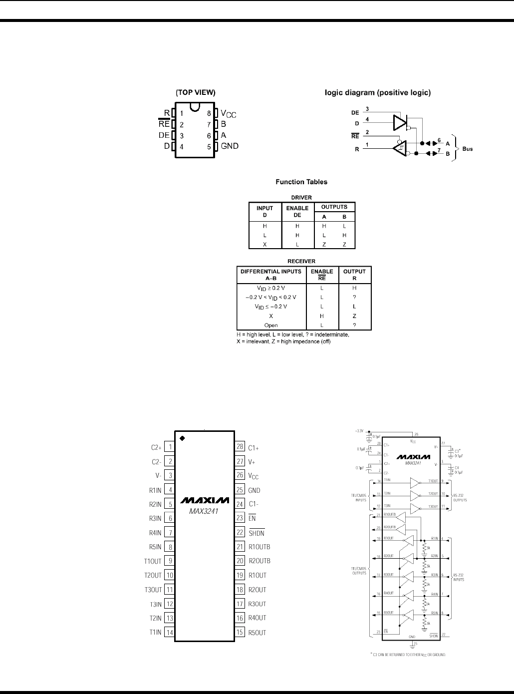
IC DATA
MM101271V1 R2A 117
U21
RS485 Transceiver
TI, 75176BD
U24
RS232 Transceiver, 3V to 5.5V, 3-TX, 5-RX
MAXIM, MAX3241CAI, SSOP28
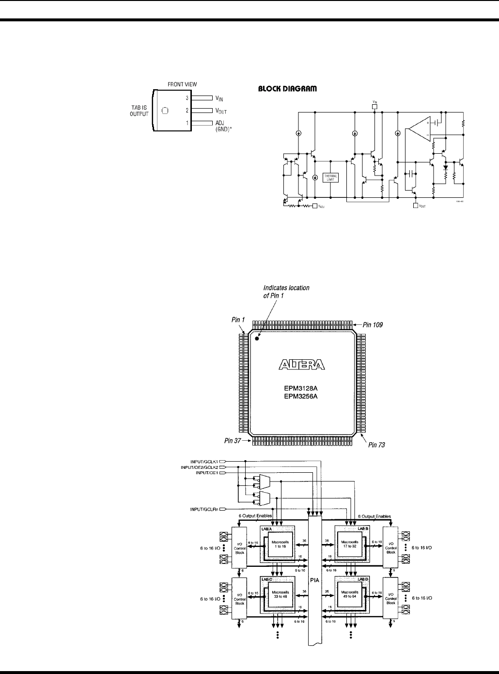
IC DATA
118 MM101271V1 R2A
U25
+5V Regulator, 1.5A
LINEAR TECH, LT1086CM-3.3
U27
144 PIN EPLD
ALTERA, EPM3256ATC144
(Refer to EPLD Drawings)
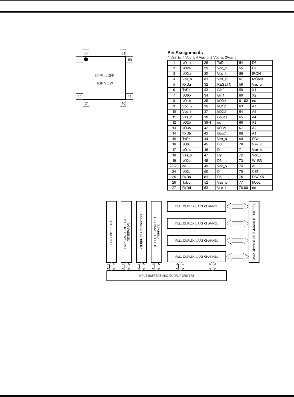
IC DATA
MM101271V1 R2A 119
U28
QUAD UART (QUART)
Philips, SC28L194A1BE
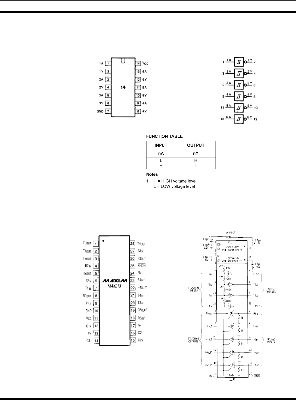
IC DATA
120 MM101271V1 R2A
U29, U32
HEX Buffer
(Philips, 74HCT14PW
U30
RS-232 Transceiver, 5V, 4-TX, 5-TX
MAXIM, MAX213CAI
IC DATA
MM101271V1 R2A 121
U31
Reset Supervisor
Dallas, DS1818R-10
U33, U34, U35, U39
HEX Open-Collector Output Drivers
Philips, 74F06AD
U36
RS232 Transceiver, 3V to 5.5V, 5-TX, 3-RX
MAXIM, MAX3237CAI
IC DATA
122 MM101271V1 R2A
U37
Hot Swap Controller
Linear Tech, LTC1422
U38
Single NAND Gate
Philips, 74AHC1G00GW
IC DATA
MM101271V1 R2A 123
U40
555 Timer
National, LMC555CM
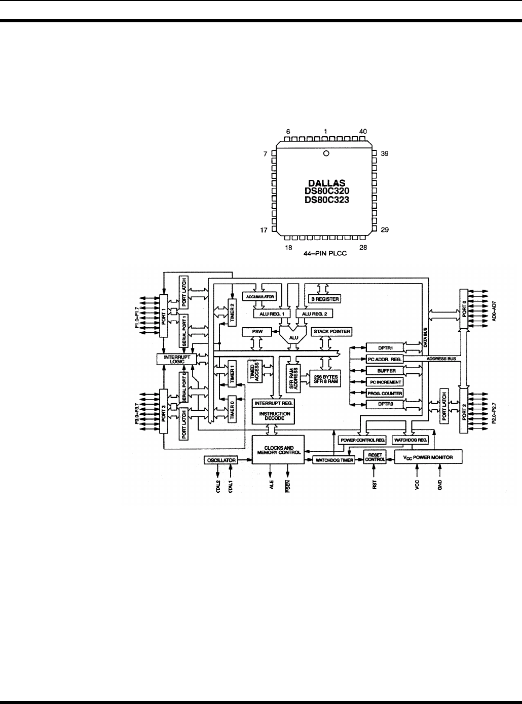
IC DATA
124 MM101271V1 R2A
12.2 SitePro MODEM BOARD (A2-A1)
U1
Microprocessor
Dallas DS80C323-QCD
IC DATA
MM101271V1 R2A 125
U2 & U4
64k x 8 SRAM
IDT71V124SA20PH
U3
Dual Port RAM
IDT70V05L55PF
Continued
IC DATA
126 MM101271V1 R2A
Continued
U5
Address Decoder
Philips 74ALVC138ADB
IC DATA
MM101271V1 R2A 127
U6
3.3V – 5V Converter
IDT74FCT164245TPA
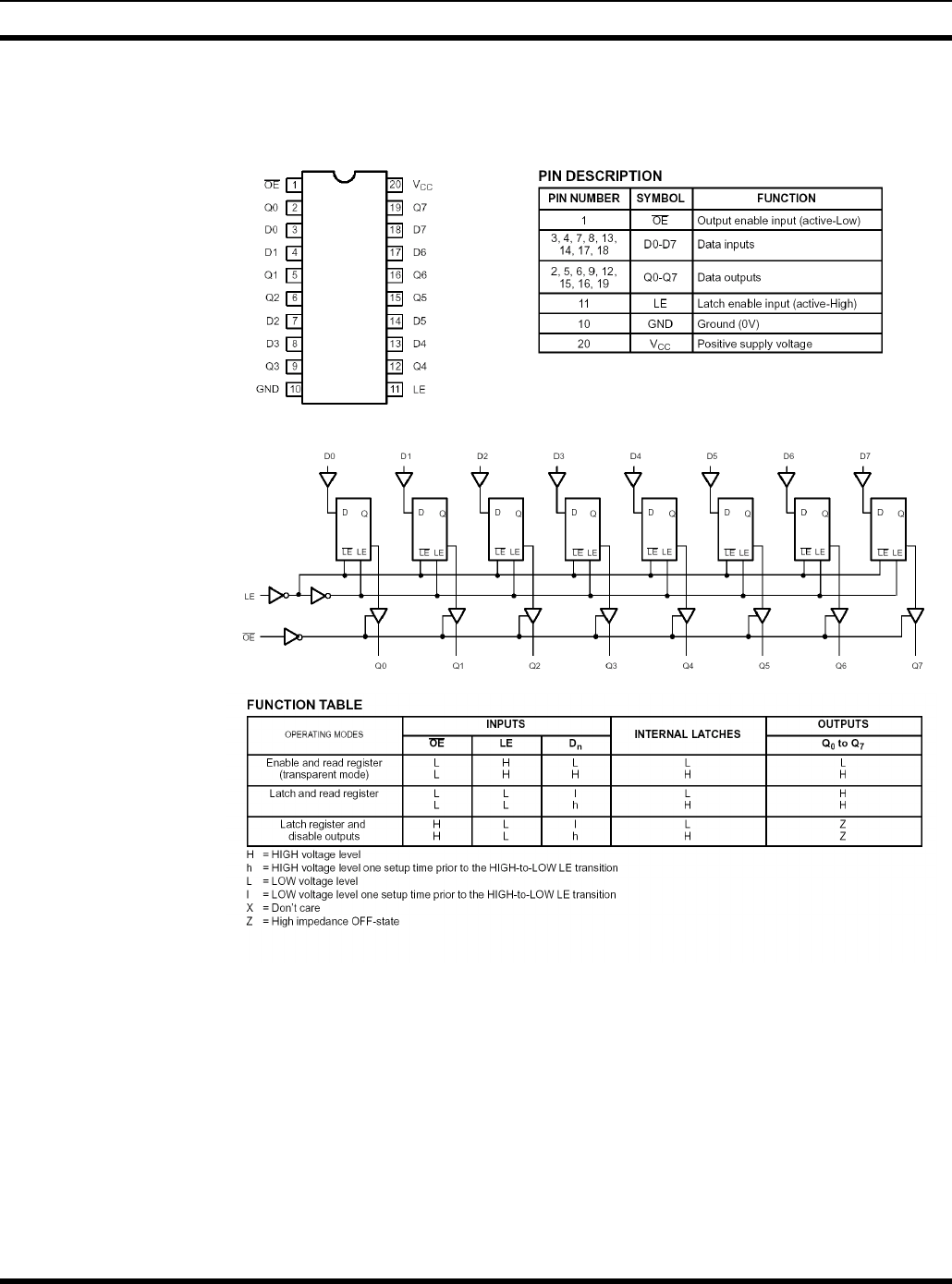
IC DATA
128 MM101271V1 R2A
U7
8-Bit Latch
Philips 74LVC373APWDH
IC DATA
MM101271V1 R2A 129
U9, U10 & U11
RF/PL/VDI Modem
Ericsson ROP 101 688/4C
CONNECTIONS
Terminal Symbol Function
1 RE Read enable (active low)
2 EN Chip enable (active low)
3 RESOUT Reset output (active high)
4 AD0 Bi-directional address/data bus
5 AD1 Bi-directional address/data bus
6 AD2 Bi-directional address/data bus
7 AD3 Bi-directional address/data bus
8 AD4 Bi-directional address/data bus
9 AD5 Bi-directional address/data bus
10 AD6 Bi-directional address/data bus
11 AD7 Bi-directional address/data bus
12 ALE Address latch enable (active high)
13 VSS Ground
14 CLK1 Buffered oscillator output
15 VDD Power Supply
16 XTAL1 Oscillator input
17 XTAL2 Oscillator output
18 CLK2 640 kHz output
19 DRAIN Received data input
20 SAT/G1 Received SAT input/G1 enable
HC138 (active high)
21 TXDAT Transmit data output
22 RCVCLK/
Q2
Recovered clock output/Q2 output
for HC138
23 RCVDAT/
Q0
Recovered data output/Q0 output
for HC138
24 INT Interrupt request (active low o.d.)
25 RESIN Reset input (active high)
26 CS Chip select (active low)
27 CLK3/4 Transmit clock output/CLK 1/6
Output
28 WR Write enable (active low)
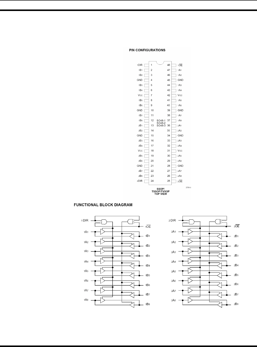
IC DATA
130 MM101271V1 R2A
U12
Adder Bus Buffer
IDT74FCT163245APF
Continued
IC DATA
MM101271V1 R2A 131
Continued
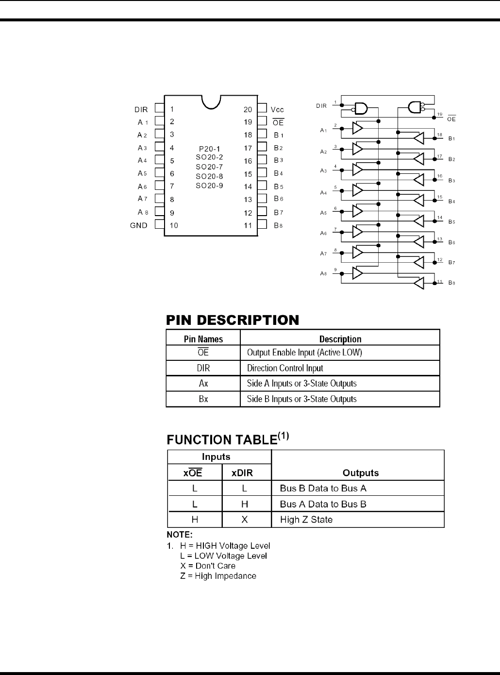
IC DATA
132 MM101271V1 R2A
U13
Data Bus Buffer
IDT74FCT3245APG
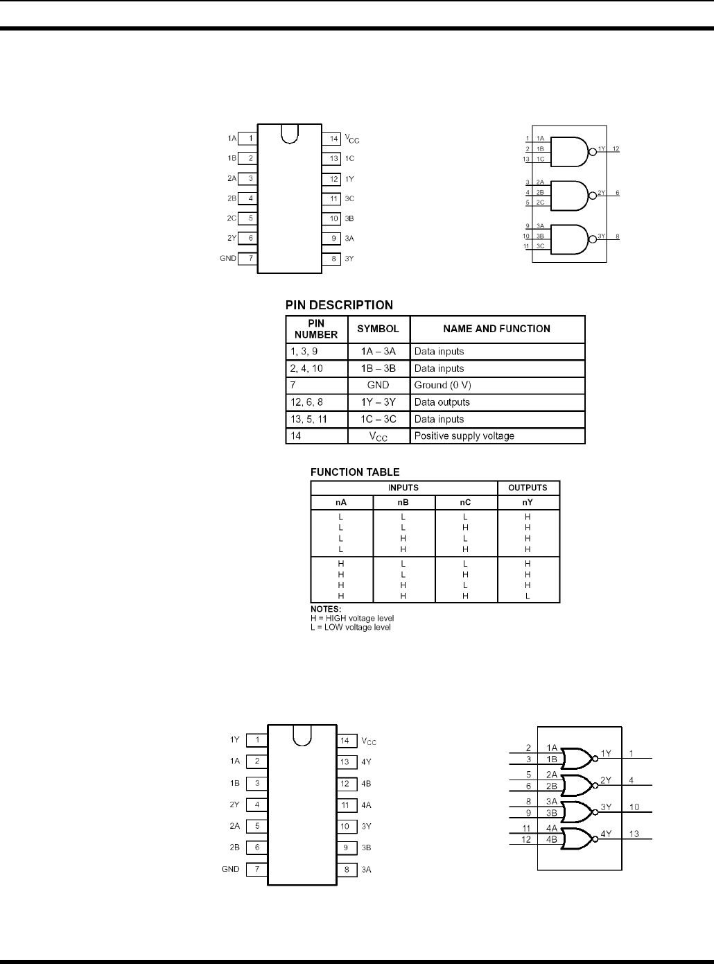
IC DATA
MM101271V1 R2A 133
U16
Triple 3-Input NAND Gates
Philips 74LVC10APWDH
U17
Quad 2-Input NOR Gates
Philips 74LVC02APWDH
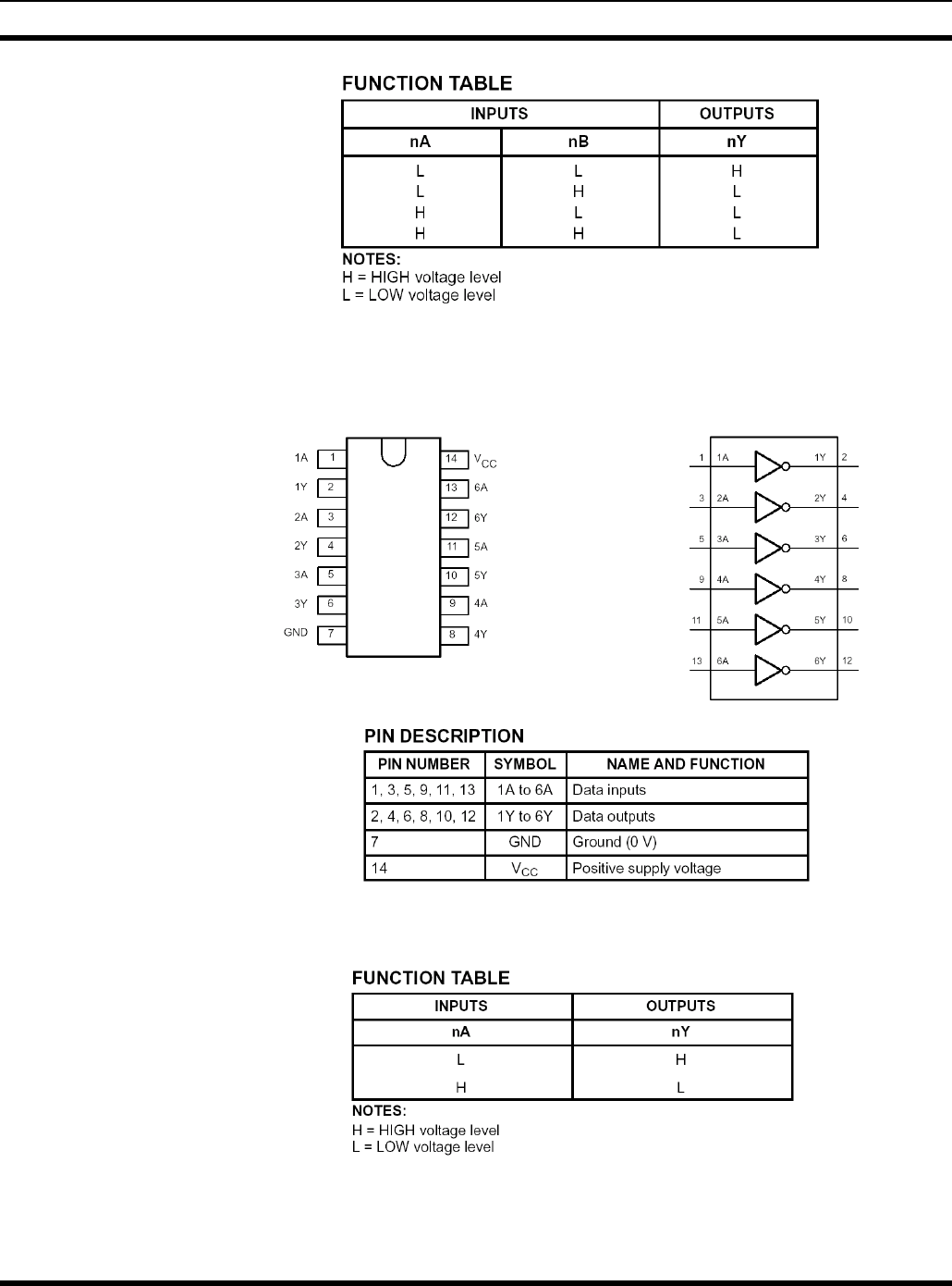
IC DATA
134 MM101271V1 R2A
U18
Inverters
Philips 74LVC04APWDH
Continued
Continued
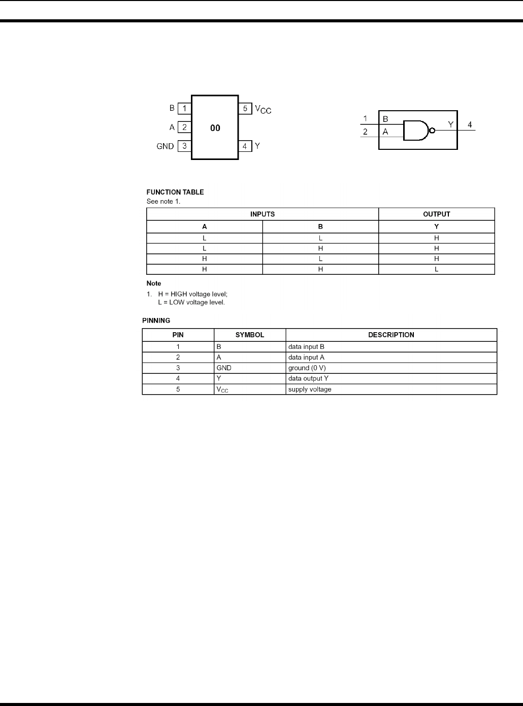
IC DATA
MM101271V1 R2A 135
U19
2-Input NAND Gate
Philips 74AHC1G00GW
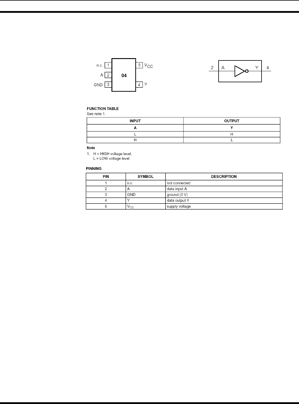
IC DATA
136 MM101271V1 R2A
U20, U21 & U22
Inverter
Philips 74AHC1G04GW
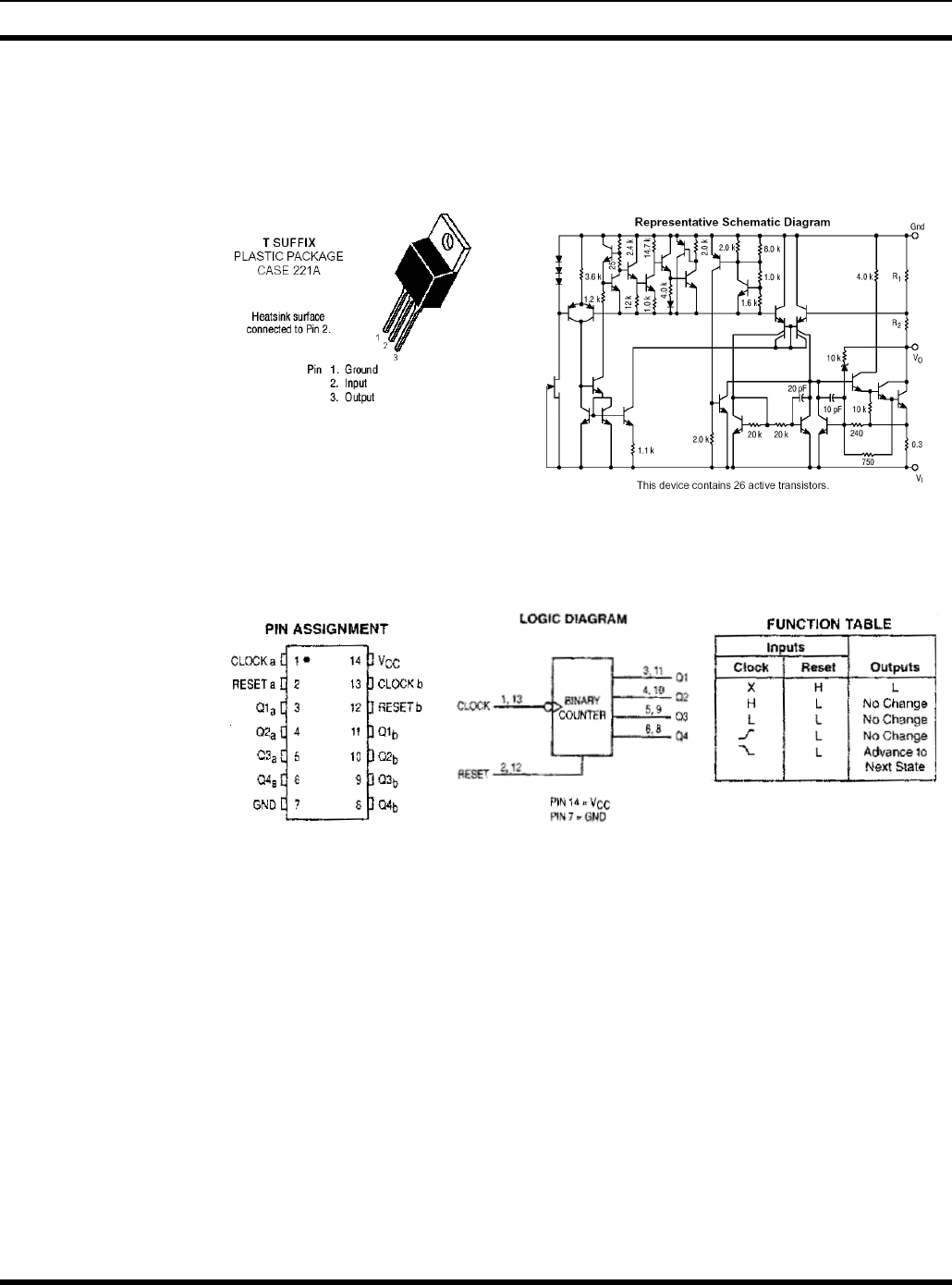
IC DATA
MM101271V1 R2A 137
12.3 ANALOG FILTER BOARD (A4)
U2
Three-Terminal Negative Fixed Voltage Regulator
Motorola, MC79M05BT
U3
Dual 4-Stage Binary Ripple Counter
Motorola, MC74HC393AD
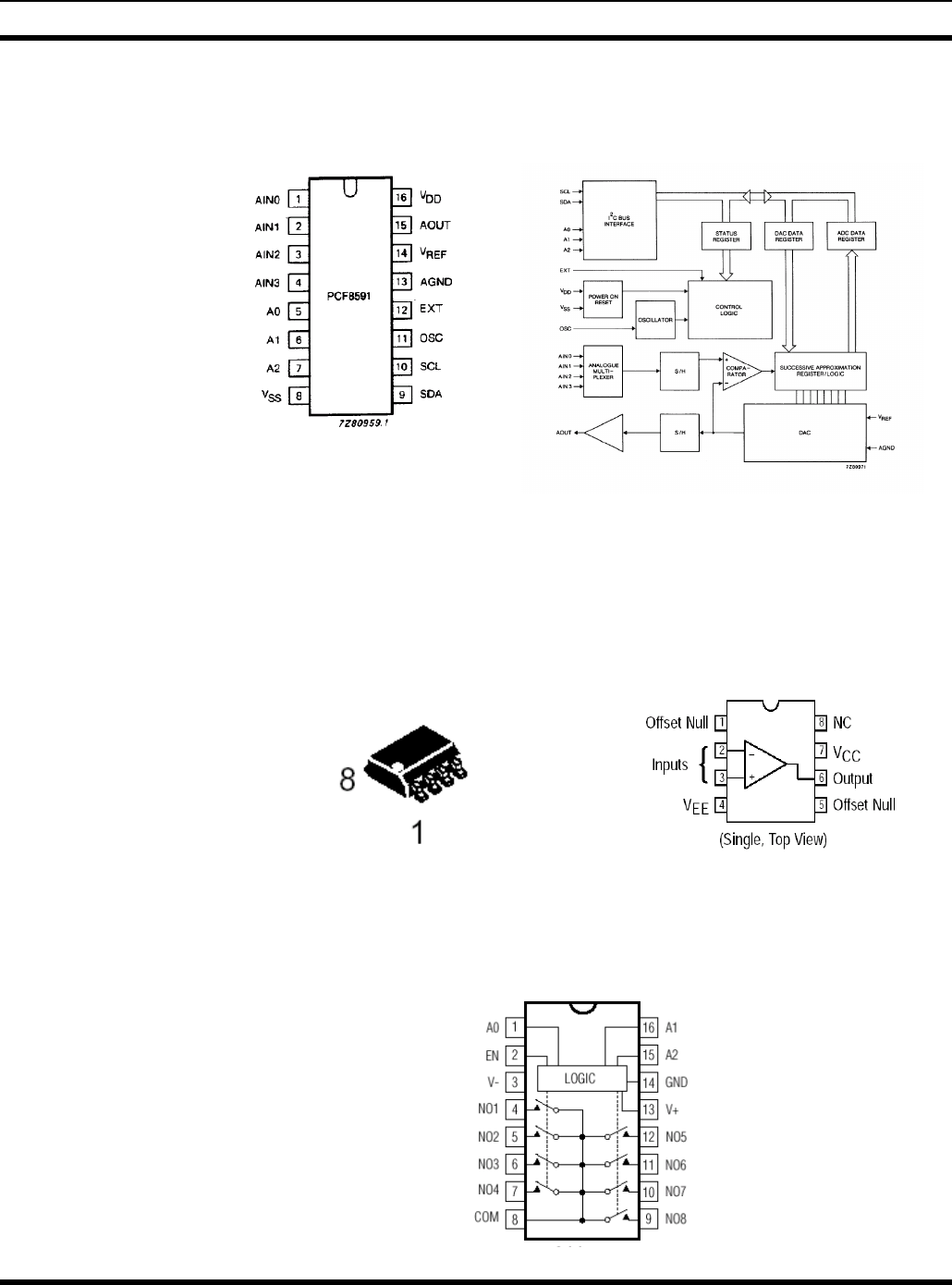
IC DATA
138 MM101271V1 R2A
U4
Remote 16-Bit I/O Expander for I2C-Bus
(Philips, PCF8575CTS
U5 & U10
High Slew Rate, Wide Bandwidth, Single Supply Operational Amplifier
Motorola, MC33074D
U6, U15, U17, U19 & U28
High Slew Rate, Wide Bandwidth, Single Supply Operational Amplifier
Motorola, MC33072D
U7
Fault-Protected, High-Voltage Single 8-to-1/Dual 4-to-1 Multiplexers
Maxim, MAX4508ESE
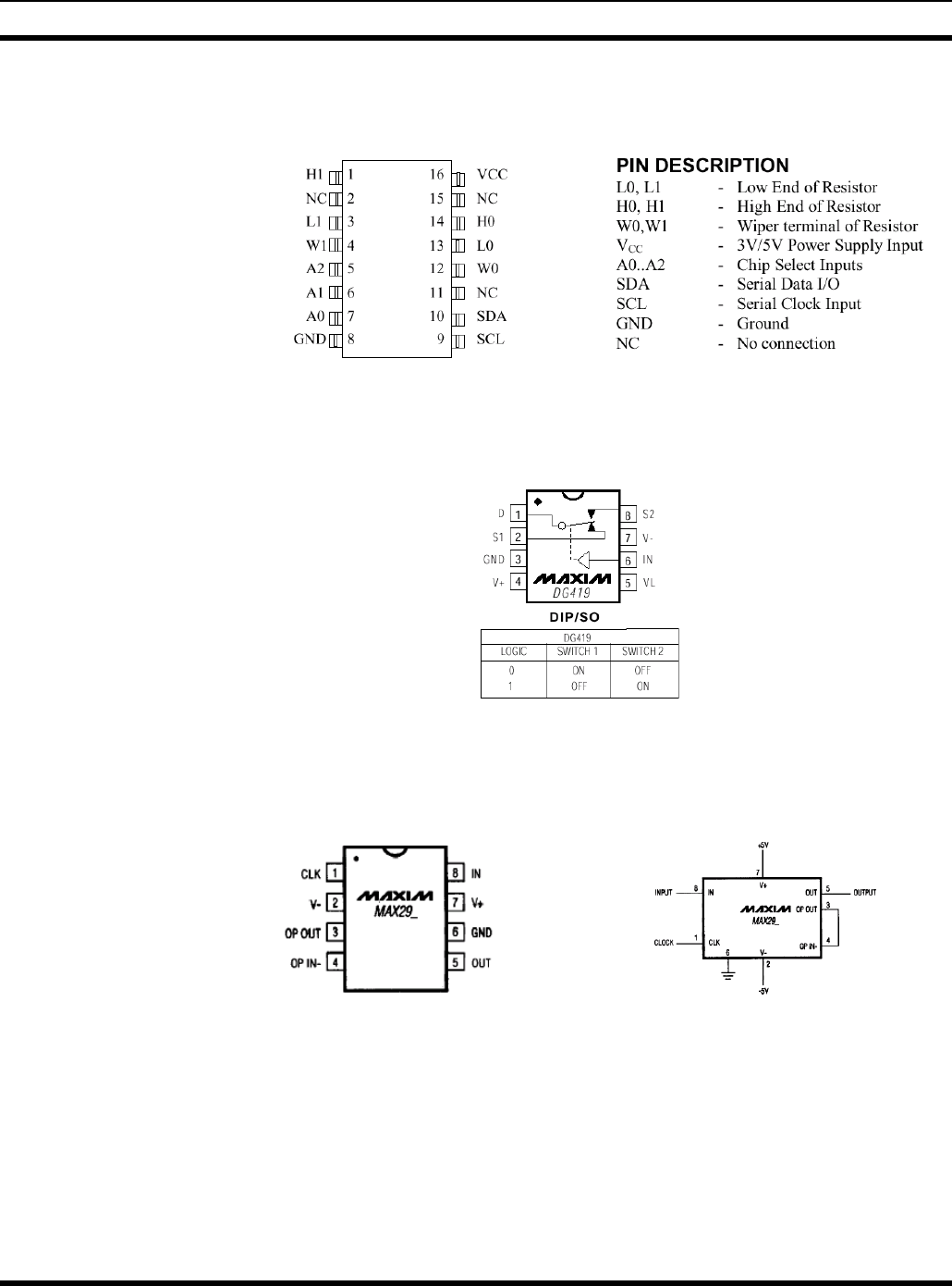
IC DATA
MM101271V1 R2A 139
U8
Addressable Dual Digital Potentionmeter
Dallas, DS1803Z-010
U9, U18 & U22
SPST/SPDT Analog Switches
Maxim, DG419DY
U11
8th-Order, Lowpass, Switched-Capacitor Filters
Maxim, MAX292ESA
IC DATA
140 MM101271V1 R2A
U12 & U33
Low Offset Voltage Dual Comparators
Motorola, LM393D
U14 & U20
8th-Order, Lowpass, Elliptic, Switched-Capacitor Filters
Maxim, MAX294EWE
CONNECTIONS
PIN NAME FUNCTION
1CLK
Clock input – use internal or
external clock.
2 V- Negative Supply pin.
Dual supplies:
-2.375V to –5.5V.
Single supply: V-= 0V.
3OP
OUT
Uncommitted Op-Amp Output
4 OP IN Inverting input to the
uncommitted op amp. The
noninverting op amp is internally
tied to GND.
5 OUT Filter Output
6GND
Ground. In single-supply
operation, GND must be biased
to the mid-supply voltage level.
7 V+ Positive Supply pin. Dual
supplies: +2.375V to +5.5V.
Single supply: +4.75V to +11.0V
8 IN Filter Input.
IC DATA
MM101271V1 R2A 141
U16 & U25
Quad Low Power RS-232 Driver
Linear Tech, LTC4861S
U21
High Performance Switched Capacitor Universal Filter
Linear Tech, LTC1059S
U23
8-Bit A/D and D/A Converter
Philips, PCF8591TD
IC DATA
142 MM101271V1 R2A
U24
+5V-Powered, Multi-Channel RS-232 Drivers/Receivers
Maxim, MAX232AESE
U26
Quad RS-485 Line Receiver
Linear Tech, LTC489S
U27
Dual Peripheral Drivers
TI, SN75451BD
IC DATA
MM101271V1 R2A 143
U31
Fault-Protected, High-Voltage, Single 4-to-1/Dual 2-to-1 Multiplexers
Maxim, MAX4534ESD
U32
HEX Inverter
Motorola, MC14069UBDR2
U34
EEPROM
Atmel AT24C128N-10SC-2.7
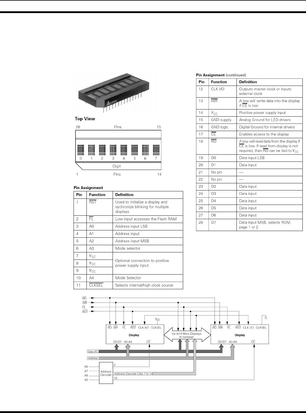
IC DATA
144 MM101271V1 R2A
12.4 DISPLAY MODULE ASSEMBLY (A6)
U1
Smart LED Display Function
Siemens HSDP2112S
IC DATA
MM101271V1 R2A 145
U2
Remote 16-bit I/O Expander for I2C
Philips PCF8575TS

146 MM101271V1 R2A
(Intentionally Left Blank)