HARRIS TR-0017-E Sitepro Base Station User Manual RX IF
HARRIS CORPORATION Sitepro Base Station RX IF
HARRIS >
Contents
RX IF

Maintenance Manual
MM101886V1 R1A
21.4 MHz RECEIVER IF MODULE
12.5/25 kHz CHANNEL SPACING
CB101128V1
TABLE OF CONTENTS
Page
1.0 SPECIFICATIONS................................................................................................................................................. 3
2.0 DESCRIPTION ...................................................................................................................................................... 4
3.0 CIRCUIT ANALYSIS............................................................................................................................................ 5
3.1 INPUT AMPLIFIER NETWORK...................................................................................................................... 5
3.2 CRYSTAL FILTERS, IF AMPLIFIER.............................................................................................................. 5
3.3 INTEGRATED CIRCUIT AGC AMPLIFIER................................................................................................... 5
3.4 OSCILLATOR/MIXER/DETECTOR................................................................................................................ 6
3.5 AUDIO AMPLIFIER ......................................................................................................................................... 6
3.6 SQUELCH.......................................................................................................................................................... 7
3.6.1 Buffer Amplifier ............................................................................................................................................. 7
3.6.2 Bandpass Filter ............................................................................................................................................... 8
3.6.3 Noise Detector ................................................................................................................................................ 8
3.6.4 DC Amplifier .................................................................................................................................................. 8
3.6.5 Schmitt Trigger............................................................................................................................................... 8
3.7 FAULT DETECTORS ....................................................................................................................................... 8
3.8 VOLTAGE REGULATORS .............................................................................................................................. 9
3.9 ADDRESS DECODER ...................................................................................................................................... 9
4.0 MAINTENANCE ................................................................................................................................................. 10
4.1 RECOMMENDED TEST EQUIPMENT......................................................................................................... 10
4.2 ALIGNMENT PROCEDURE.......................................................................................................................... 10
4.3 CRYSTAL FILTER TUNING ......................................................................................................................... 11
4.3.1 Tuning FL1 and FL2..................................................................................................................................... 11
4.3.2 Tuning FL3 and FL4..................................................................................................................................... 11
4.4 AUDIO AND DATA OUTPUT ADJUSTMENTS.......................................................................................... 11
4.5 TROUBLESHOOTING.................................................................................................................................... 11
5.0 ASSEMBLY DIAGRAM..................................................................................................................................... 13
6.0 PARTS LIST ........................................................................................................................................................ 14
7.0 IC DATA .............................................................................................................................................................. 23
8.0 OUTLINE DIAGRAM......................................................................................................................................... 30
9.0 SCHEMATIC DIAGRAM ................................................................................................................................... 31

2MM101886V1 R1A
This manual is published by M/A-COM Private Radio Systems, Inc., without any warranty. Improvements and changes to this manual
necessitated by typographical errors, inaccuracies of current information, or improvements to programs and/or equipment, may be made by
M/A-COM Private Radio Systems, Inc., at any time and without notice. Such changes will be incorporated into new editions of this
manual. No part of this manual may be reproduced or transmitted in any form or by any means, electronic or mechanical, including
photocopying and recording, for any purpose, without the express written permission of M/A-COM Private Radio Systems, Inc.
Copyright© 2002, M/A-COM Private Radio Systems, Inc. All rights reserved.
NOTE
This device made under license under one or more of the following US patents: 4,590,473; 4,636,791; 5,148,482; 5,185,796;
5,271,017; 5,377,229.
NOTE
The voice coding technology embodied in this product is protected by intellectual property rights including patent rights,
copyrights, and trade secrets of Digital Voice Systems, Inc. The user of this technology is explicitly prohibited from
attempting to decompile, reverse engineer, or disassemble the Object Code, or in any other way convert the Object Code into
human-readable form.

SPECIFICATIONS
MM101886V1 R1A 3
1.0 SPECIFICATIONS1
Item Specification
I.F. (Intermediate Frequency) 21.4 MHz
Input Impedance 50 ohm
l2 dB SINAD ≤-120 dBm (25 kHz); ≤-119 dBm (12.5 kHz)
Adj. CH Rejection ≥85 dB (25 kHz); ≥80 dB (12.5 kHz)
Image Rejection ≥100 dB
Intermodulation Rejection ≥83 dB (25 kHz); ≥78 dB (12.5 kHz)
Signal Displacement Bandwidth ≥2 kHz (25 kHz); ≥1 kHz (12.5 kHz)
2nd I.F. (Intermediate Frequency) 455 kHz
455 kHz Balanced Output Level 2.2 V PP per line, adjustable
2nd L.O. Frequency 20.945 MHz
AF Output (J2, Pin 31C) 1 Vrms adjustable (with standard input signal)
AF Output Impedance 1k ohm
AF Distortion ≤3% (25 kHz); ≤5% (12.5 kHz)
AF Response
10 Hz ≥-3 dB ref.
300 Hz ±1 dB ref.
1000 Hz 0 dB reference
3 kHz (25 kHz Channel) ±1.6 dB ref.
3 kHz (12.5 kHz Channel) ± 2.5 dB ref.
Hum & Noise Rejection ≥55 dB (25 kHz); ≥50 dB (12.5 kHz)
RSSI Output (J2, Pin 20C) 0.7 to 2.7 VDC
RSSI Time Constant 5 ms
SQ Threshold Sensitivity ≤-123 dBm (25 kHz); ≤-122 dBm (12.5 kHz)
SQ Maximum Sensitivity ≤-110 dBm (25 kHz); ≤-109 dBm (12.5 kHz)
SQ Clipping 3 kHz
SQ Attack 150 ms
SQ Close 250 ms
SQ Output (J2, Pin 26C) 5V logic (low = squelched)
Fault Output (J2, Pin 11C) 5V logic (low = fault)
AGC Range 50 dB
DC Supply 13.8V, 80 mA max.; 12.0V, 65 mA max.
1 These specifications are intended to be used by the service technician during servicing. Refer to the appropriate
Specification Sheet for the complete Specification.
DESCRIPTION
4MM101886V1 R1A
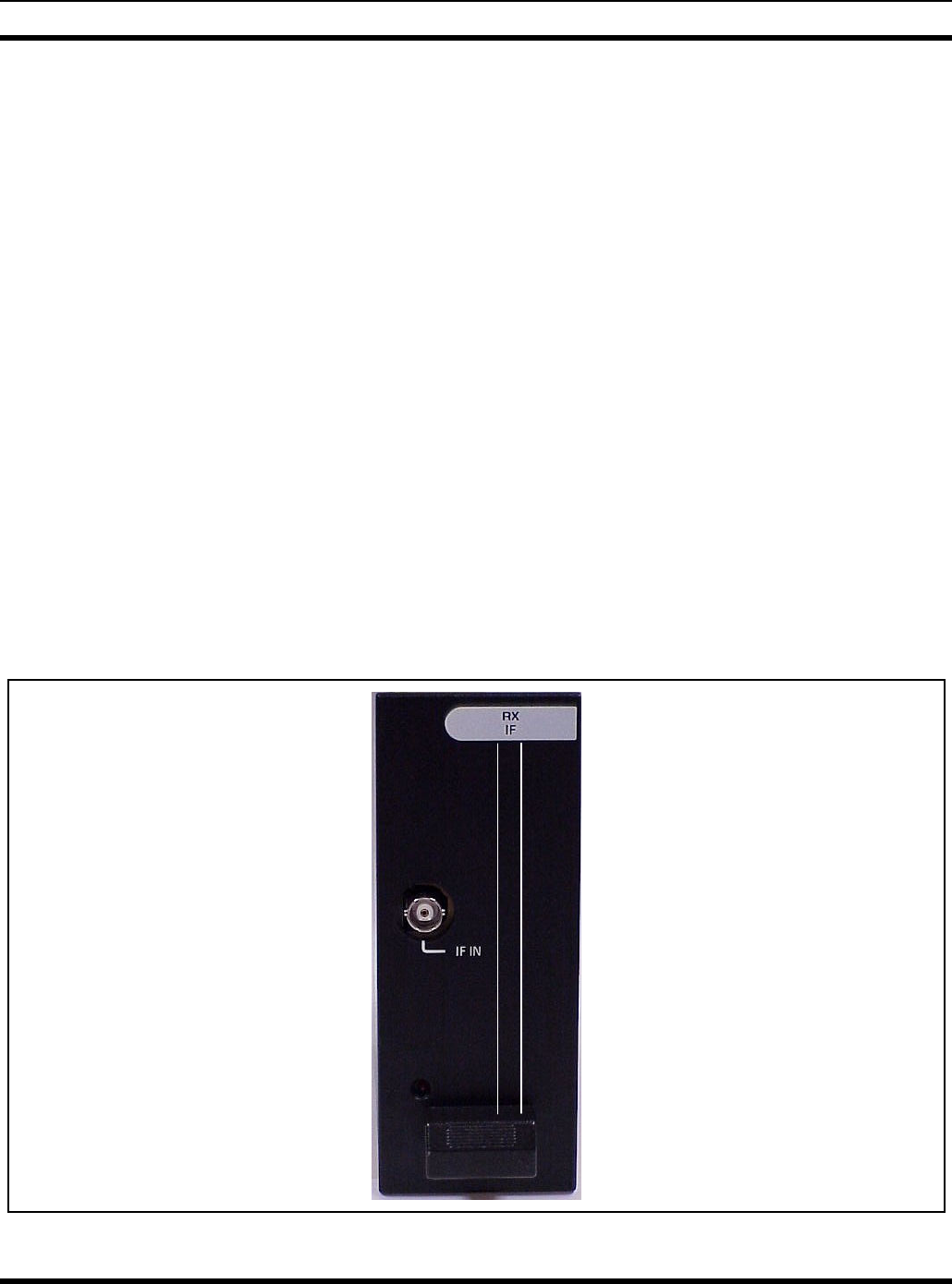
2.0 DESCRIPTION
The MASTR III Receiver IF Module 19D902783G7/G11 provides amplification and
demodulation of the 21.4 MHz Intermediate Frequency (IF) signal as well as Automatic
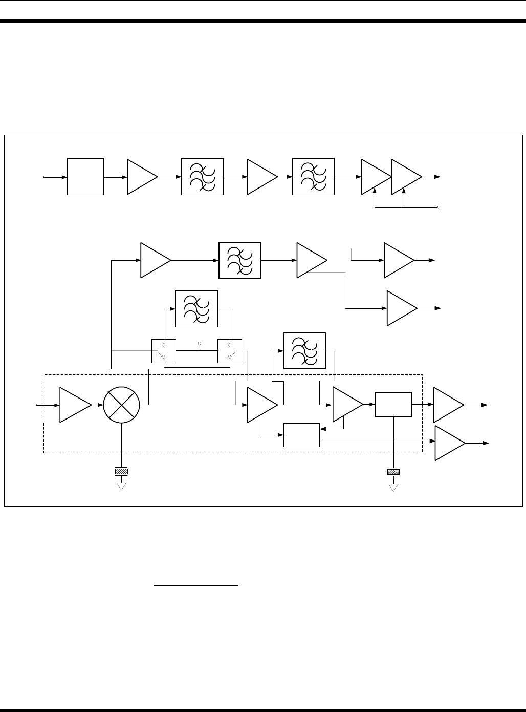
Gain Controlled (AGC) 455 kHz outputs to the DSP Modem module(Figure 1 - 21.4
MHz Receiver IF Module). The IF Module also includes the receiver squelch circuitry.
However, it does not include de-emphasis or squelch audio gating circuits. Figure 2 –
21.4 MHz IF Module Block Diagram shows the functional operation of the IF Module.
The IF Module circuitry contains the following:
•A 50 ohm input impedance IF Amplifier
•A chain of four crystal filters and IF amplifier
• A two stage AGC amplifier
• A two stage balanced output IF amplifier
•An integrated circuit containing a crystal oscillator, mixer, limiter, and quadrature
detector
•A variable gain AF amplifier
•A squelch circuit
•A fault detector circuit
•An integrated circuit voltage regulator
•An address decoder
Figure 1 - 21.4 MHz Receiver IF Module

CIRCUIT ANALYSIS
MM101886V1 R1A 5
3.0 CIRCUIT ANALYSIS
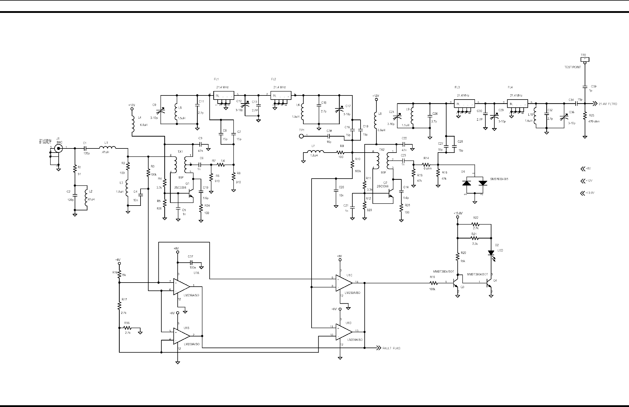
3.1 INPUT AMPLIFIER NETWORK
The input amplifier consisting of transistor Q1 and transformer TX1, provides a 50 ohm
load for the receiver IF module.
Capacitor C1 provides AC coupling and a DC block on the input line (J1). This DC block
protects the module in the event of a failure in a preceding module.
Capacitor C1 and inductor L1 are series-resonant at 21.4 MHz and provide a low-
impedance path from J1 to amplifier transistor Q1. Capacitor C2 and inductor L2 are
parallel-resonant at 21.4 MHz and provide a path to the 50-ohm load, resistor R1, for
mixer products other than 21.4 MHz.
3.2 CRYSTAL FILTERS, IF AMPLIFIER
Crystal Filters FL1, FL2, FL3 and FL4, transistor Q2 circuit, and associated circuitry
provide IF filtering and amplification at 21.4 MHz. Filters FL1 and FL2 are two pole
crystal bandpass filters centered at 21.4 MHz with a typical combined 6 dB bandwidth of
±7.0 kHz. The loss of FL1 and FL2 combined is typically between 2.5 and 3.5 dB. When
combined, the filter set has associated matching networks to match the combination to a
50-ohm input and output impedance. FL3 and FL4 are matched to a 50-ohm input
impedance and a 470 ohm output impedance. The FL1 and FL2 pair is specified to have
especially good intermodulation performance to meet the overall requirements for the
module.
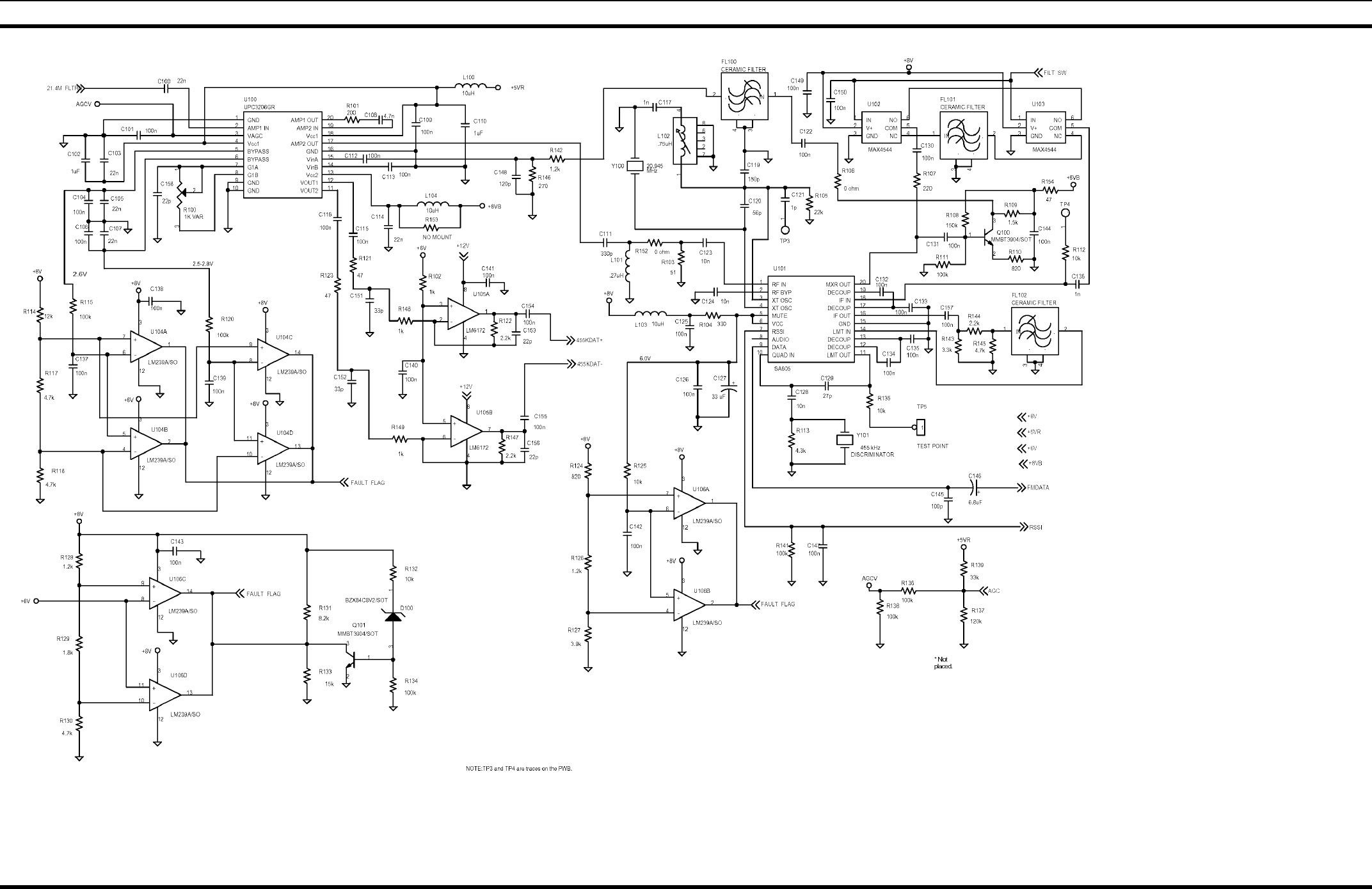
3.3 INTEGRATED CIRCUIT AGC AMPLIFIER
The first two stages of AGC Amplifier U100 consist of two IF amplifiers whose gain can
be controlled with an AGC voltage. These two amplifiers are connected in cascade to
combine their gains. The combined voltage gain varies from about 35 dB at an AGC
voltage of 3.5 VDC down to about –25 dB at an AGC voltage of <1.5 VDC. The AGC
voltage is supplied by the DSP Modem module. In the two level FM mode, when no DSP
modem is present, the AGC voltage is set to a fixed voltage of 3.5 volts by voltage
divider resistors R139 and R137 to set the cascaded AGC amplifier gain to maximum.
The output of the second IF amplifier in U100 feeds the 21.4 MHz IF signal to the input
of U101 through a matching network consisting of inductor L101 and capacitor C123.
The matching network matches the output impedance of the second IF amplifier in U100
to resistor R103.
The video amplifier has a single ended voltage gain (from the input to one output) of
from 25 to 43 dB. The gain is set in this range by adjusting resistor R100. The differential
gain is 6 dB higher than the single ended gain. The input of this stage comes from the IC
mixer U101 output by way of 455 kHz filter FL100. Filter FL100 has a 6 dB bandwidth
of ±7.5 kHz to reduce the level of adjacent channel signals passing into the DSP Modem
module. The differential output of the video amplifier is routed to U105, and then to the
DSP Modem module via the Backplane board.

CIRCUIT ANALYSIS
6MM101886V1 R1A
3.4 OSCILLATOR/MIXER/DETECTOR
Integrated circuit U101 performs several functions. The 20.945 MHz crystal oscillator
provides local oscillator injection to the mixer in U101. This mixer converts the 21.4
MHz IF signal to 455 kHz. Capacitors C119 and C120 are oscillator feedback capacitors
and have been chosen to provide the proper capacitance for crystal Y100. The frequency
can be adjusted by means of L102. The proper oscillator output level is difficult to
measure directly without affecting the circuit operation. The level at TP3 should be
approximately 50 mVpk (Measured using a 10 megohm, 1lpF oscilloscope probe).
The mixer is internally connected to the crystal oscillator. Pins 1 and 20 of U101 are the
mixer input and output respectively. Typical mixer conversion voltage gain is
approximately 12 dB. The mixer output feeds the transistor Q100 IF amplifier circuit and
each analog switch, U102 and U103. The output from Q100 is routed to ceramic filter
FL100. In the 12.5 kHz bandwidth mode, analog switches U102 and U103 route the 455
kHz IF through FL101 to the U101 IF amplifier input. In the 25 kHz mode, the mixer
output is switched around FL101 by U102 and U103 and is then routed to the IF
amplifier input. In the four level FM mode, FL101 is bypassed as in the 25 kHz two level
mode. Ceramic filters FL101 and FL102 have a minimum 6dB bandwidth of 455 kHz
±6kHz.
The IF amplifier input is U101, Pin 18. The output at U101, Pin 16 is passed through an
attenuator consisting of resistors R143, R144, and R145 to ceramic bandpass filter
FL102, then to the limiter input at U101, Pin 14. The limiter output drives one input of
the quadrature detector via capacitor C129.
A Received Signal Strength Indicator (RSSI) is provided at U101, Pin 7. This indicator
signal is generated within the limiter circuitry and provides an output current proportional
to the logarithm of the input signal strength. This current develops a voltage across
resistor R141. The voltage varies from about 1.6 VDC for noise input, to about 2.4 VDC
for a 12 dB SINAD signal, to a maximum of about 4.7 VDC for a –75 dBm IF input
signal at J1. RSSI Buffer U200A provides buffering to eliminate loading effects on the
RSSI line. The RSSI line will provide a constant output level above a –75 dBm IF input
level, since the input to U101 is held constant by AGC from the DSP Modem module.
The quadrature detector provides a demodulated audio frequency output. One input to the
detector is internally connected to the limiter and is not externally available. The output
of the detector is at U101, Pin 9. Capacitor C145 provides lowpass filtering to remove
455 kHz feed-through. Ceramic resonator Y101 provides the frequency-selective
component needed for FM demodulation. Y101 replaces the typical LC resonant circuit
found in most quadrature detectors. In contrast to the typical LC network, Y101 requires
no adjustment. In the four level FM mode, the detector output of U101 is not used. The
detected audio output is derived by other circuitry in the base station.
Integrated circuit U101 general: The DC supply to U101 is provided through voltage
dropping resistor Rl04 to U101, Pin 6. The voltage drop across resistor R104 is used to
monitor the dc voltage on U101 for fault detection.
3.5 AUDIO AMPLIFIER
Operational amplifier U200C provides audio frequency amplification. The gain of
U200C is set by associated resistors, including variable resistor R203. Resistor R203
allows adjustment of the AF output level to 1 Vrms with a standard input signal to the
CIRCUIT ANALYSIS
MM101886V1 R1A 7
module (1 kHz AF, 3 kHz peak deviation in the 25 kHz mode).
The typical amplifier gain is approximately 5. In the 12.5 kHz mode the standard
deviation is 1.5 kHz. To provide the same 1 Vrms output, the gain is increased by
shunting resistor R202 with resistor R201 by means of electronic switch U207.
Operational amplifier U200B is used as a voltage regulator to provide 6 VDC for biasing
U200C.
DIPLEXER
WB/NB
DETECTOR
RSSI
21.4 MHz
IF IN
IF AMP
21
.
4
MHz
XTAL FILTER
AGC
AMP
UPC3206
AGC IN FROM
DSP MODEM
455 kHz TO
DSP MODEM
TO FM
IF IC
SA605 FM IF IC
U101
21
.
4
MH
z
XTAL FILTER
IF AMP
IF AMP MIXER
IF AMP LIMITER AUDIO
AMP
DATA
OUT
RSSI
OUT
455 kHz
CER FILT
FL101
455 kHz
CER FILT
FL102
455 kHz
CER FILT
BUFER AMP
LM6172
BUFFER AMP
UPC3206C
21.4 MHz
FM IF
IC IN
20.945
MHz
455
kHz
RSSI
BUFFER
Q1 FL1,FL2 Q2 FL3,FL4 U100A,B
IF BUFFER AMP
Q100
FL100 U100C
U105A
U105B
U102 U103
U200C
U200A
+
-
455 kHz
DISCRIMINATOR
Figure 2 – 21.4 MHz IF Module Block Diagram
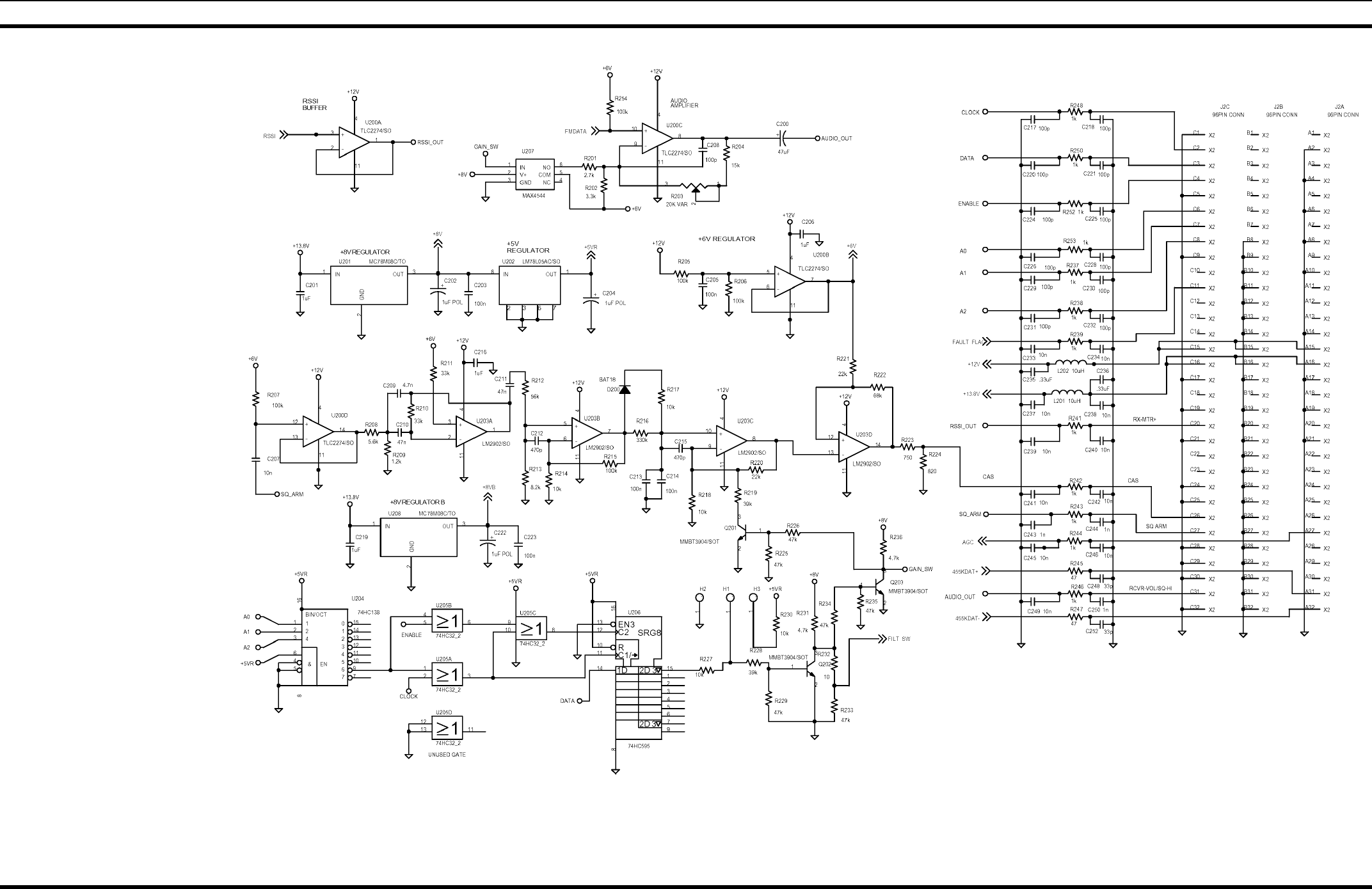
3.6 SQUELCH
3.6.1 Buffer Amplifier
Buffer amplifier U200D (Refer to Schematic Diagram WD-CB101128V1, Sh. 3) is
configured as a unity gain buffer amplifier. Its purpose is to provide a high input
impedance in order to minimize loading of preceding circuitry.

CIRCUIT ANALYSIS
8MM101886V1 R1A
3.6.2 Bandpass Filter
Bandpass filter U203A, together with its associated circuitry, performs the function of an
audio frequency bandpass filter, centered at 6 kHz with a gain of 2. The purpose of this
filter is to reject all voice frequencies and allow only demodulated noise to pass. The
functioning of the squelch circuit depends upon the presence or absence of this noise.
When a signal is being received, i.e. the receiver is “quiet”, the squelch circuit senses the
absence of noise and unsquelches the radio.
3.6.3 Noise Detector
Noise detector U203B along with associated components are configured as an amplifier.
A single +12 V dc supply powers this op-amp, therefore the output can only be positive.
Because the ac noise input goes both positive and negative U203B effectively acts as a
rectifier with gain. The rectified output of U203B charges capacitors C213 and C214 to a
nearly constant dc voltage. (Actually the R216-C213,C214 time constant will allow a 5
Hz variation.)
3.6.4 DC Amplifier
DC amplifier U203C is configured as a basic amplifier with a gain of 5.0 in the 25 kHz
mode. In the 12.5 kHz mode, the gain is increased by about 6 dB by shunting resistor
R218 with resistor R219 by means of transistor switch Q201.
3.6.5 Schmitt Trigger
Schmitt trigger U203D is configured as an amplifier with positive feedback. This
arrangement provides hysteresis in the output versus input characteristic. This eliminates
the possibility of the squelch circuit repeatedly cutting in and out when the input signal is
near a threshold. Resistors R223 and R224 act as a voltage divider to provide a 5 volt
logic level output.
3.7 FAULT DETECTORS
Voltage comparators U1, U104, and U106 are configured as "window detectors," which
pull the FAULT DETECT line low (approximately 0 volts) if the voltage applied falls
outside the specified range (window). For example: U106C senses whether the input
voltage is greater than the upper limit of the window. This limit is set by the voltage
divider R128, R129, and R130 (6.75 VDC). Comparator U106D senses whether the input
is less than the lower limit of the window (4.88 VDC, again set by R128, R129, and
R130). Therefore, in this example the window is 4.88 VDC to 6.75 VDC. The
U106C/U106D window detector circuit is used to determine whether the U200D voltage
regulator output (+6 VDC) is within this range. The other window detector circuits
monitor dc operating voltages on transistors Ql and Q2 and integrated circuits U100 and
U101 respectively.
Resistors R131 and R133 comprise a voltage divider to provide a 5 V logic level output.
Also, these resistors act as a pull-up for the open collector comparators. A fault is
indicated when the output drops to zero.
Diode Dl00 and transistor Q101 monitor the output of the 8 V regulator. Dl is a 8.2 Volt
Zener diode. If the regulator output voltage should rise above 8.9 V (8.2 + 0.7 base-

CIRCUIT ANALYSIS
MM101886V1 R1A 9
emitter drop) Q101 will turn on and a fault will be indicated. Transistors Q3 and Q4 are
drivers for the front panel LED D2. These are powered from the +13.8VDC supply.
Therefore, if the 8V regulator opens, a fault will still be indicated.
3.8 VOLTAGE REGULATORS
8V regulator U201 is a monolithic integrated circuit voltage regulator providing 8 VDC
(+8V). This powers all 8-volt circuitry in the module with the exception of U100 and
Q100. A second 8 volt regulator, U208, supplies 8 VDC (+8VB) to U100 and Q100.
5V regulator U202 is a monolithic integrated circuit voltage regulator that provides
5VDC to U100, U204, U205, and U206. This regulator operates from the 8 VDC
provided by U201.
3.9 ADDRESS DECODER
The address decoder circuit consists of binary-to-octal converter U204, quad or-gate
U205, and eight bit shift register U206.
When a low (0) is present on the A0 line, and a high (1) on the A1 and A2 lines, U204,
Pin 9 provides a low to U205A and U205B. When there is a clock input to U205A and an
enable input to U205B, the output of U250C provides a latch clock input to U206, Pin 12,
and U205A provides a shift clock input to U206, Pin 11. When U206 is enabled, it
detects the data on the DATA input at Pin 14. Internal flip-flops latch the data to hold the
output state on Pin 15. Depending on the data, U206, Pin 15 is either high for the
narrowband (12.5 kHz) mode or low for the wideband (25 kHz) mode. A “high” is a
voltage greater than 3.5 VDC, and a “low” is a voltage less than 1.0 VDC.
3.10 BUFFER AMPLIFIER U105
Operational amplifier U105 amplifies the 455kHz output from the video amplifier in
U100 to a maximum level of 2.2 V peak-to-peak. The differential output of U105 is
routed to J2, Pins A31 and A32. The differential signal passes through the backplane
board to the DSP Modem module. Buffer amplifier U105 has a voltage gain of
approximately 2.

MAINTENANCE
10 MM101886V1 R1A
4.0 MAINTENANCE
4.1 RECOMMENDED TEST EQUIPMENT
The following test equipment is required to test the IF Module
1. FM Signal Generator; HP 8640B, HP 8657A, or equivalent
2. AF Generator or Function Generator
3. Audio Analyzer; HP 8903B, HP 339A, or equivalent
4. Oscilloscope
5. Frequency Counter; Racal-Dana 9919 or equivalent
6. DC Meter for troubleshooting
7. Power Supply; 13.8 VDC @ 180 mA
8. Power Supply; 12 VDC @40 mA
9. M/A-COM Test Box TS101285V11
4.2 ALIGNMENT PROCEDURE
1. Apply 13.8 VDC and 12 Vdc supplies to the IF module.
2. Verify 13.8 VDC current consumption is between 55 and 80 mA, and 12 VDC
current is between 45 and 65 mA.
NOTE
The currents cannot be measured directly when the TS11285V11 test box is used. The
currents can be determined by measuring the voltage drop across L201 and L202 on
the Receiver IF printed wire board and the resistance of each coil. The current can be
calculated with the following formula:
I = Vdrop/Rcoil
3. Set the AGC switch on the test box to "HIGH."
4. Verify fault output is 0 to 0.5 VDC and front panel LED is off.
5. Apply a standard input signal to the module input (-75 dBm, 21.4 MHz signal
modulated with 1 kHz AF, 3 kHz peak deviation).
6. Monitor TP5 with a high-impedance probe connected to the frequency counter.
Adjust inductor L102 for a reading of 455 kHz ± 100 Hz.
7. Set variable resistor R203 for 1 Vrms ±3% at module output (pin 31C on 96 pin
connector J2).
MAINTENANCE
MM101886V1 R1A 11
4.3 CRYSTAL FILTER TUNING
4.3.1 Tuning FL1 and FL2
1. Connect test equipment as shown in Fig. 10.1.
2. Connect the high impedance probe to either side of resistor R152.
3. Set the span of the network analyzer to 20 kHz, and the center frequency to 21.4
MHz.
4. Set the analyzer RF output level to obtain –75 dBm at the input of the module.
5. Adjust C9, C12, and C17 for maximum response at 21.4 MHz.
4.3.2 Tuning FL3 and FL4
1. Adjust C24, C29, and C36 for maximum response at 21.4 MHz.
2. The 6 dB bandwidth displayed on the network analyzer shall be between fc +/- 6.1
and fc +/- 7.3 kHz. The peak-to-valley ripple shall be less than 1 dB.
3. If the requirements of step 2 are not met, adjust C9, C12, C17, C24, C29, and C36 as
needed until the requirements are met.
NOTE
The bandwidth is controlled primarily by C12 and C29.
4. Set the squelch pot on the test fixture to maximum (maximum means to set the wiper
for maximum signal at the Sq-Arm terminal)
4.4 AUDIO AND DATA OUTPUT ADJUSTMENTS
1. In the 25 kHz mode, apply a standard input signal (-75 dBm, 21.4000 MHz signal
modulated with a 1kHz Audio Frequency (AF), 3kHz peak deviation) to the module
IF input. Turn the FM modulation off. Monitor TP5 with a high impedance probe
connected to the frequency counter. Adjust L102 for a reading of 455 kHz ±100 Hz.
2. Turn the RF generator FM modulation on. Set R203 for 1.0 Vrms ±3% AF output at
module output (Pin 31C on 96 pin connector, Pin 52).
3. Remove the FM modulation from the test signal. Monitor the 455kHz+ jack on the
test box with an oscilloscope using a high-impedance probe. Adjust R100 for a
2.2±0.1 volts peak-to-peak level. The 455 kHz-jack shall have a level of 2.2 ± 0.2 V
peak-to-peak.
4.5 TROUBLESHOOTING
When troubleshooting the module, it is most convenient if the standard test fixture is
used. The following conditions are with the module in the 25 kHz mode. This can be set
up using a PC with the necessary software connected to the test box. Alternatively, a wire
link can be soldered between pads H1 and H2 on the PC board.
MAINTENANCE
12 MM101886V1 R1A
IF amplifier transistor Q2 has a nominal 8 dB gain. Transistor Q2 has a nominal gain of
8.5 dB. The mixer has about 14 dB voltage gain with proper LO injection. The proper
crystal oscillator level is 10 mV pk measured at TP3.
The following four test points are provided on the PWB for additional test capability:
TP1: 45 mV pk @ 21.4 MHz with -20 dBm input signal
TP3: 10 mV pk @ 20.945 MHz independent of input signal
TP4: 20 mV pk @ 455 kHz with -60 dBm input signal
TP5: 750 mV pk @ 455 kHz with -75 dBm input signal
All RF voltages measured with 10 Megohm, 11 pF probe.
Table 1 - Troubleshooting Guide
SYMPTOM CHECK
(CORRECT READING SHOWN)
INCORRECT READING
INDICATES DEFECTIVE
COMPONENT
Fault indicator
on
Check DC voltages:
+8V @ U201, Pin 3
+6V @ U200, Pin 7
1.5V @ Q1 and Q2 (emitters)
6V @ U101, Pin 5
If DC voltages not correct
U201 or associated components
U200 or associated components
Q1 and Q2 or associated components
U101 or associated components
No audio - no
noise
With no signal applied to module IF input:
Check for AF noise @ C146; 200mV
Check for AF noise @ U200, Pin 8; 1 V
U101 or associated components
U200 or associated components
Noise only -
no
demodulated
audio
Check crystal oscillator:
TP3, 10 mVpk, 20.945 MHz
Apply -30 dBm, 21.4 MHz input, check TPl 60 mVpk
Apply -60 dBm, 21.4 MHz input, check TP4 20 mVpk
U101, Y100 or associated components
Q1, FL1, FL2 or associated components
Q2, FL3, FL4, Y101, U100 or associated
components
Poor 12 dB
SINAD
Check crystal oscillator:
TP3, 10 mVpk, 20.945 MHz
Apply -30 dBm, 21.4 MHz input, check TP1, 60 mVpk
Apply -60 dBm 21.4 MHz input, check TP4, 20 mVpk
U101, Y100 or associated components
Q1, FL1, FL2, Y100, or associated components
Q2, FL3, FL4, U100, U101 FL102 or associated
components
With squelch pot maximum, or with module AUDIO/
SQUELCH/HI connected to SQUELCH/ARM input and
with no signal to module IF input:
Check Presence of 1 Vpk noise @ U200, Pin 14
Check presence of 1 Vpk noise U7 @t Pin 12 U200 or associated components
No squelch
function
Check DC voltage U203 @t Pin 8: 7V
Check DC voltage U203 @ Pin 14: 0.5V U203 or associated components
ASSEMBLY DIAGRAM
MM101886V1 R1A 13
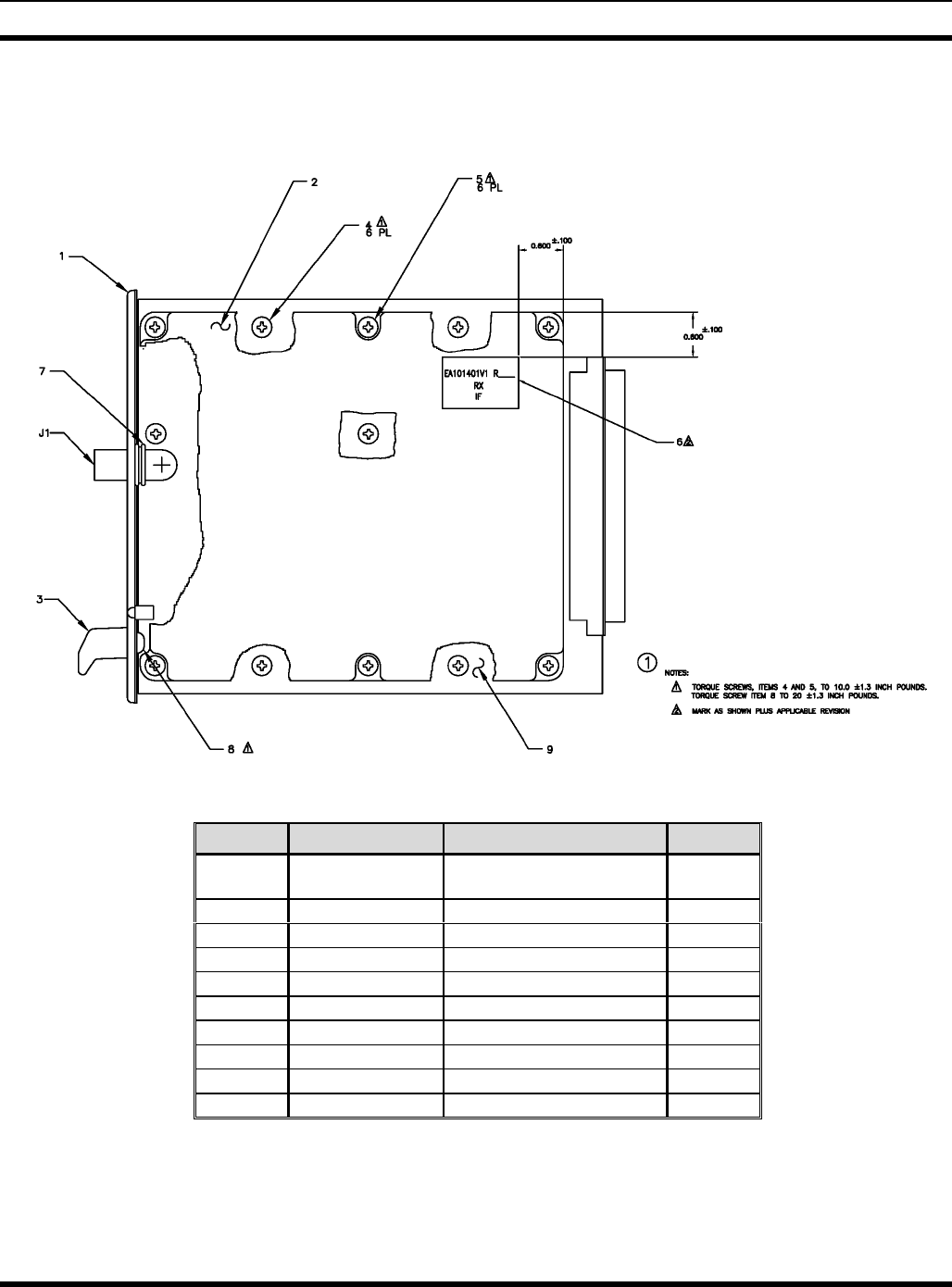
5.0 ASSEMBLY DIAGRAM
Item Part Number Description Qty
21.4 MHz Receiver IF
Module EA101401V1
119D902508P1 Chassis 1
219D902509P1 Cover 1
319D902555P1 Handle 1
419A702381P506 Screw, torq 6
519A702381P513 Screw, torq 6
619B235310P1 NP, Blank 1
719B802690P1 Grommet 1
819A702381P508 Screw, torq 1
9CB101128V1 Board, Component 1
RECEIVER IF MODULE
EA101401V1
(AD-EA101401, Rev. A)

PARTS LIST
14 MM101886V1 R1A
6.0 PARTS LIST
MASTR III RECEIVER IF CIRCUIT BOARD ASSEMBLY
PL-CB101128V12 Revision: A
Symbol Part Number Description
- - - - CAPACITORS - - -
C1
and
C2
RJC 463 4043/12 120pF
C3 RJC 464 2045/47 47nF
C4 RJC 464 2045/1 10nF
C5 RJC 464 3044/47 4.7nF
C6 RJC 464 2045/1 10nF
C7
and
C8
RJC 463 6042/15 15pF
C9 19A704350P102 3-10pF: MURATA
C10 RJC 463 4042/33 33pF
C11 RJC 463 9041/27 2.7pF
C12 19A704350P102 3-10Pf: MURATA
C13 RJC 463 9041/27 2.7pF
C14
and
C15
RJC 463 9041/56 5.6pF
C16 RJC 463 9041/27 2.7pF
C17 19A704350P102 3-10pF: MURATA
C18
and
C19
RJC 463 6042/15 15pF
C20 RJC 464 2045/1 10nF
C21 RJC 464 3044/47 4.7nF
C22 RJC 464 2045/47 47nF
C23 RJC 464 2045/1 10nF
C24 19A704350P102 3-10pF: MURATA
C25 RJC 463 4042/33 33pF
C26 RJC 463 9041/27 2.7pF
C27
and
C28
RJC 463 6042/15 15pF
C29 19A704350P102 3-10pF: MURATA
C30 RJC 463 9041/27 2.7pF
C31 RJC 464 3044/47 4.7nF
C32 RJC 463 9041/27 2.7pF
C33 RJC 464 3044/47 4.7nF
C34 RJC 463 6042/15 15pF
2 COMPONENTS ADDED, DELETED OR CHANGED BY PRODUCTION CHANGES.

PARTS LIST
MM101886V1 R1A 15
Symbol Part Number Description
C35 Not Used
C36 19A704350P102 3-10pF
C37 RJC 464 3046/1 100nF
C38 RJC 463 4042/1 10pF
C39 RJC 463 0041/1 1pF
C40
thru
C99
Not Used
C100
and
C101
RJC 464 3045/22 22nF
C102 RJC 464 3067/1 1µF.
C103 RJC 464 3045/22 22nF
C104 RJC 464 3046/1 100nF
C105, RJC 464 3045/22 22nF
C106 RJC 464 3046/1 100nF
C107 RJC 464 3045/22 22nF
C108 RJC 464 3044/47 4.7nF
C109, RJC 464 3046/1 100nF
C110, RJC 464 3067/1 1µF
C111 RJC 463 4043/33 330pF
C112 RJC 464 3046/1 100nF
C113 RJC 463 4044/1 1nF
C114 RJC 464 3045/22 22nF
C115
and
C116
RJC 464 3046/1 100nF
C117 RJC 463 4044/1 1nF
C118 Not Used
C119 RJC 463 4043/15 150pF
C120 RJC 463 4042/56 56pF
C121 RJC 463 0041/1 1pF
C122 RJC 464 3046/1 100nF
C123
and
C124
RJC 464 2045/1 10nF
C125
and
C126
RJC 464 3046/1 100nF
C127 19A705205P15 33 µF
C128 RJC 464 2045/1 10nF
C129 RJC 463 4042/27 27pF
C130
thru
C135
RJC 464 3046/1 100nF
C136 RJC 463 4044/1 1nF

PARTS LIST
16 MM101886V1 R1A
Symbol Part Number Description
C137
and
C138
RJC 464 3046/1 100nF
C139 RJC 463 4042/22 22pF
C140
thru
C144
RJC 464 3046/1 100nF
C145 RJC 463 4043/1 100pF
C146 19A705205P5 6.8µF
C147 RJC 464 3046/1 100nF
C148 RJC 463 4043/12 120pF
C149
and
C150
RJC 464 3046/1 100nF
C151
and
C152
RJC 463 6042/15 15pF
C153, RJC 463 4042/22 22pF
C154
and
C155
RJC 464 3046/1 100nF
C156 RJC 463 4042/22 22pF
C157 RJC 464 3046/1 100nF
C158 RJC 463 4042/22 22pF
C159
thru
C199
Not Used
C200 19A705205P111 47µF
C201, RJC 464 3067/1 1µF
C202 19A705205P2 1µF POL
C203 RJC 464 3046/1 100nF
C204 19A705205P2 1µF POL
C205 RJC 464 3046/1 100nF
C206 RJC 464 3067/1 1µF
C207 RJC 464 2045/1 10nF
C208, RJC 463 4043/1 100pF
C209 RJC 464 3044/47 4.7nF
C210
and
C211
RJC 464 2045/47 47nF
C212 RJC 463 4043/47 470pF
C213
and
C214
RJC 464 3046/1 100nF
C215 RJC 463 4043/47 470pF
C216 RJC 464 3067/1 1µF
C217
and
RJC 463 4043/1 100pF

PARTS LIST
MM101886V1 R1A 17
Symbol Part Number Description
C218
C219 RJC 464 3067/1 1µF
C220
and
C221
RJC 463 4043/1 100pF
C222 19A705205P2 1µF POL
C223 RJC 464 3046/1 100nF
C224
thru
C226
RJC 463 4043/1 100pF
C227 Not Used
C228
thru
C232
RJC 463 4043/1 100pF
C233
and
C234
RJC 464 2045/1 10nF
C235
and
C236
RJC 464 3046/33 0.33µF
C237
thru
C242
RJC 464 2045/1 10nF
C243
and
C244
RJC 463 4044/1 1nF
C245
and
C246
RJC 464 2045/1 10nF
C247 Not Used
C248 RJC 463 4042/33 33pF
C249 RJC 464 2045/1 10nF
C250 RJC 463 4044/1 1nF
C251 Not Used
C252 RJC 463 4042/33 33pF
- - - - DIODES - - - -
D1 RKZ 323 661/5 SMS7630-005: ALPHA IND
D2 19A703595P10 LED: AGILENT TECH
D100 19A700083P105 BZX84C8V2/SOT: ON SEMI
D200 19A700155P2 BAT18: PHILIPS SEMI
- - - - FILTERS - - - -
FL1
and
FL2
Fl101061V1 21.4 MHz (High IP3 filter set consists of a matched
pair): TEW
FL100 VECFUM455E 455 kHz Ceramic Filter: MURATA
FL101
and
FL102
VECFUM455F 455 kHz Ceramic Filter: MURATA

PARTS LIST
18 MM101886V1 R1A
Symbol Part Number Description
- - - - CONNECTORS - - - -
J1 19A115938P24 BNC
J2 19B801587P7 96 PIN
- - - - INDUCTORS - - - -
L1
and
L2
REG704593/47 0.47µH: TDK
L3
and
L4
REG704594/68 6.8µH: TDK
L5
and
L6
VELQS33N1R5G04 1.5µH: MURATA
L7
and
L8
REG704594/68 6.8µH
L9 VELQS33N1R5G04 1.5µH: MURATA
L10 REG 704 14/31 3.3µF
L100 REG 704 14/37 10µH.
L101 REG 704 593/27 0.27µH: TDK
L102 19A703311P1 0.75µH: Toko
L103 REG 704 14/37 10µH
L201
and
L202
REG 704 14/37 10µH
- - - - TRANSISTORS - - - -
Q1,Q2 19A704708P2 NE85633: CEL (NEC)
Q3
and
Q4
19A700076P2 MMBT3904/SOT: ON SEMI
Q100
and
Q101
19A700076P2 MMBT3904/SOT: ON SEMI
Q201
thru
Q203
19A700076P2 MMBT3904/SOT: ON SEMI
- - - - RESISTORS - - - -
R1 344A3304P51R1 51.1 Ohms
R2 344A3304P1000 100 Ohms
R3 344A3304P1002 10k Ohms
R4 344A3304P3321 3.32k Ohms
R5 344A3304P8250 825 Ohms
R6 344A3304P9090 909 Ohms
R7 19B801251P5R6 5.62 Ohms

PARTS LIST
MM101886V1 R1A 19
Symbol Part Number Description
R8 344A3304P9090 909 Ohms
R9 344A3304P1000 100 Ohms
R10 344A3304P1002 10k Ohms
R11 344A3304P3321 3.32k Ohms
R12 344A3304P8250 825 Ohms
R13 344A3304P9090 909 Ohms
R14 19B801251P5R6 5.62 Ohms
R15 344A3304P9090 909 Ohms
R16
and
R17
344A3304P3321 3.2k Ohms
R18 344A3304P6811 6.81k Ohms
R19 344A3304P1003 100k Ohms
R20 344A3304P1502 15k Ohms
R21 344A3304P2211 2.21k Ohms
R22 344A3304P2741 2.74k Ohms
R23 344A3304P4750 475 Ohms
R24
and
R25
344A3304P1000 100 Ohms
R26
and
R27
344A3304P6811 6.81k Ohms
R28
thru
R34
Not Used
R35 Not Used
R36
thru
R99
Not Used
R100 REL 316 1114/1 1K VAR
R101 344A3304P2000 200 Ohms
R102 344A3304P1001 1k Ohms
R103 344A3304P51R1 51.1 Ohms
R104 344A3304P3320 332 Ohms
R105 344A3304P2212 22.1k Ohms
R106 19B801251P1 0 Ohms
R107 344A3304P2210 221 Ohms
R108 344A3304P1503 150k Ohms
R109 344A3304P1501 1.5k Ohms
R110 344A3304P8250 825 Ohms
R111 344A3304P1003 100k Ohms
R112 344A3304P1002 10k Ohms
R113 344A3304P4321 4.32k Ohms
R114 344A3304P3321 3.32k Ohms
R115 344A3304P6811 6.81k Ohms
R117 344A3304P3321 3.32k Ohms

PARTS LIST
20 MM101886V1 R1A
Symbol Part Number Description
R118 344A3304P6811 6.81k Ohms
R119 Not Used
R120 344A3304P1212 12.1k Ohms
R121 344A3304P4750 475 Ohms
R122 344A3304P2211 2.21k Ohms
R123 344A3304P4750 475 Ohms
R124 344A3304P8250 825 Ohms
R125 344A3304P1002 10k Ohms
R126 344A3304P1211 1.21k Ohms
R127 344A3304P3921 3.92k Ohms
R128 344A3304P1211 1.21k Ohms
R129 344A3304P1821 1.82k Ohms
R130 344A3304P4751 4.75k Ohms
R131 344A3304P8251 8.25k Ohms
R132 344A3304P1002 10k Ohms
R133 344A3304P1502 15k Ohms
R134 344A3304P1003 100k Ohms
R135 344A3304P1002 10k Ohms
R136 344A3304P6812 68.1k Ohms
R137 344A3304P1213 121k Ohms
R138 344A3304P1003 100k Ohms
R139 344A3304P3322 33.2k Ohms
R140 Not Used
R141 344A3304P1003 100k Ohms
R142 344A3304P1211 1.21k Ohms
R143 344A3304P3321 3.32k Ohms
R144 344A3304P2211 2.21k Ohms
R145 344A3304P4751 4.75k Ohms
R146 344A3304P2670 267 Ohms
R147 344A3304P2211 2.21k Ohms
R148
and
R149
344A3304P4750 475 Ohms
R150
and
R151
Not Used
R152
and
R153
19B801251P1 0 ohm.
R154 344A3304P47R5 47.5 Ohms
R155 344A3304P4750 475 Ohms
R156
thru
R200
Not Used
R201 344A3304P2741 2.74k Ohms
R202 344A3304P3321 3.32k Ohms
R203 REL 316 1115/2 20K VAR.

PARTS LIST
MM101886V1 R1A 21
Symbol Part Number Description
R204 344A3304P1502 15k Ohms
R205
thru
R207
344A3304P1003 100k Ohms
R208 344A3304P6811 6.81k Ohms
R209 344A3304P1001 1k Ohms
R210
and
R211
344A3304P3322 33.2k Ohms
R212 344A3304P5622 56.2k Ohms
R213 344A3304P8251 8.25k Ohms
R214 344A3304P1002 10k Ohms
R215 344A3304P1003 100k Ohms
R216 344A3304P3323 332k Ohms
R217
and
R218
344A3304P1002 10k Ohms
R219 344A3304P3922 39.2k Ohms
R220
and
R221
344A3304P2212 22.1k Ohms
R222 344A3304P6812 68.1k Ohms
R223 344A3304P7500 750 Ohms
R224 344A3304P8250 825 Ohms
R225
and
R226
344A3304P4752 47.5k Ohms
R227 344A3304P1002 10k Ohms
R228 344A3304P3922 39.2k Ohms
R229 344A3304P4752 47.5k Ohms
R230 344A3304P1002 10k Ohms
R231 344A3304P4751 4.75k Ohms
R232 344A3304P10R0 10 Ohms
R233
thru
R235
344A3304P4752 47.5k Ohms
R236 344A3304P4751 4.75k Ohms
R237
thru
R239
344A3304P1001 1k Ohms
R240 Not Used
R241
thru
R244
344A3304P1001 1k Ohms
R245 344A3304P47R5 47.5 Ohms
R246 344A3304P1001 1k Ohms
R247 344A3304P47R5 47.5 Ohms
R248 344A3304P1001 1k Ohms

PARTS LIST
22 MM101886V1 R1A
Symbol Part Number Description
R249 Not Used
R250 344A3304P1001 1k Ohms
R251 Not Used
R252
and
R253
344A3304P1001 1k Ohms
R254 344A3304P1003 100k Ohms
- - - - TEST POINTS - - - -
TP1 A trace on the printed wire board
TP2 344A3367P1 TEST POINT
TP3
and
TP4
Traces on the printed wire board
TP5 344A3367P1 TEST POINT
- - - - TRANSFORMERS - - - -
TX1,TX2 REGUA10003/1 B5F
- - - - INTEGRATED CIRCUITS - - - -
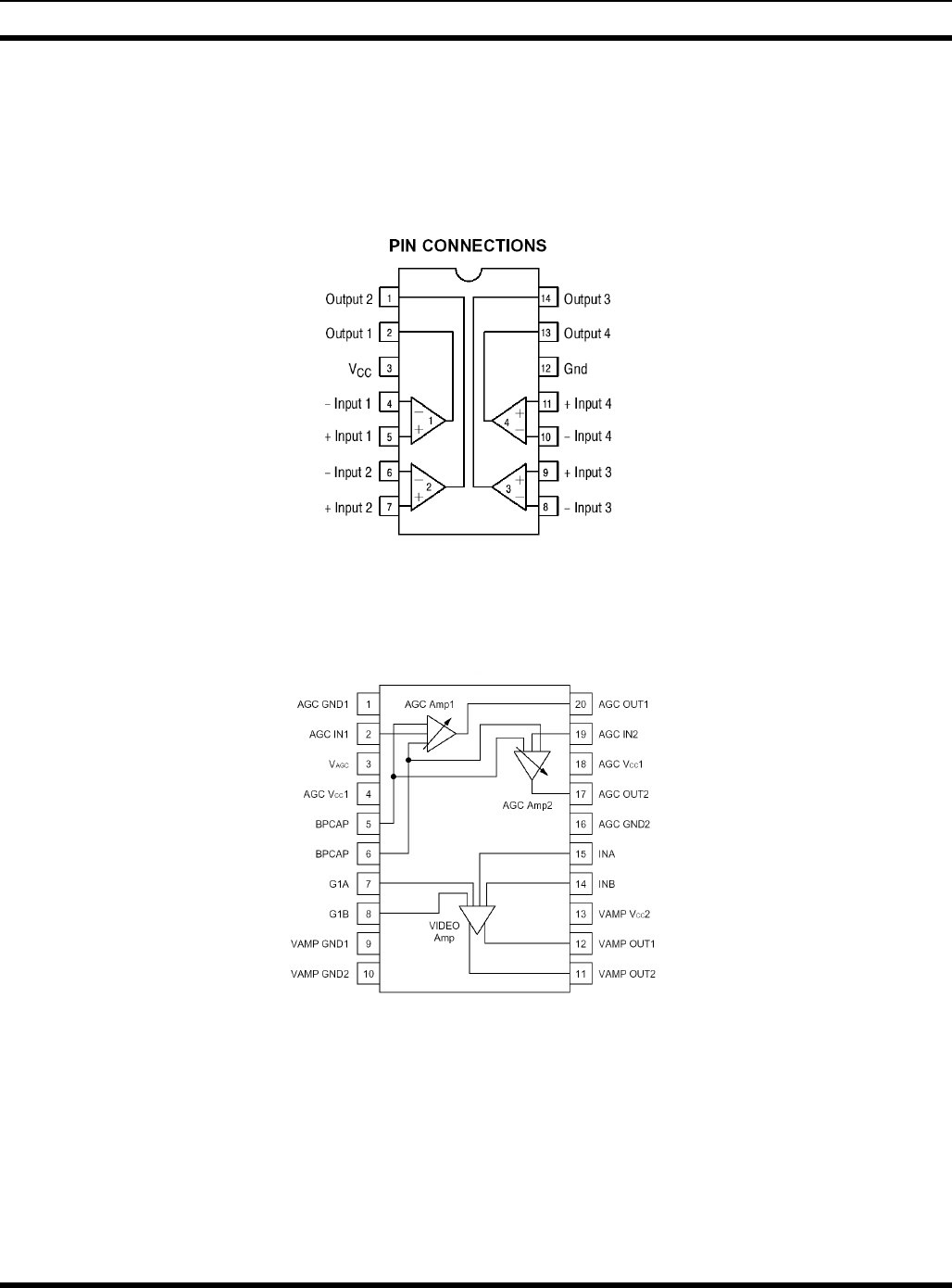
U1 GNLM239D Quad Operational Amplifier LM239A/SO: ON SEMI
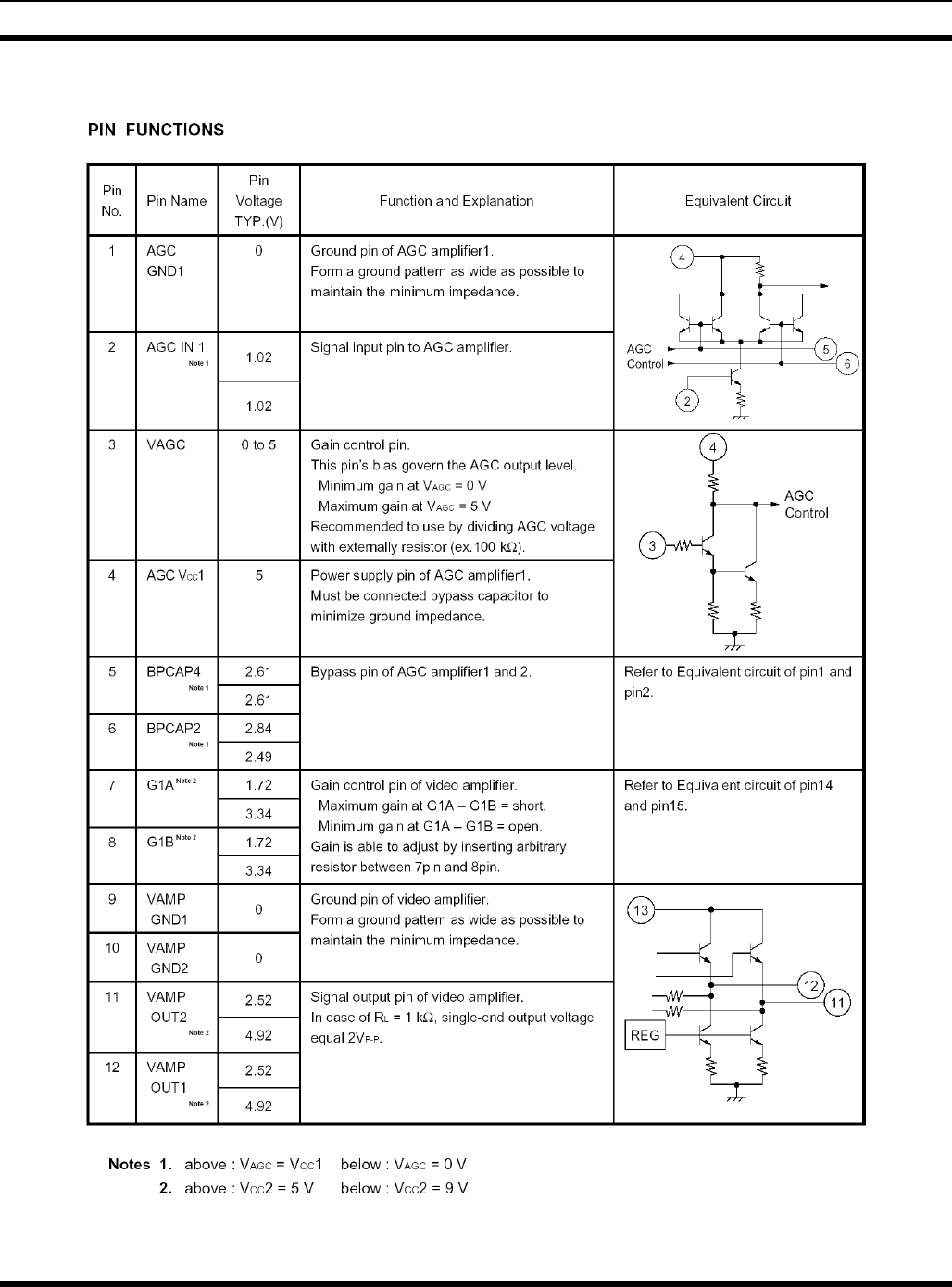
U100 VEUPC3206GR-E1 Automatic Gain Control Amplifier UPC3206GR: NEC
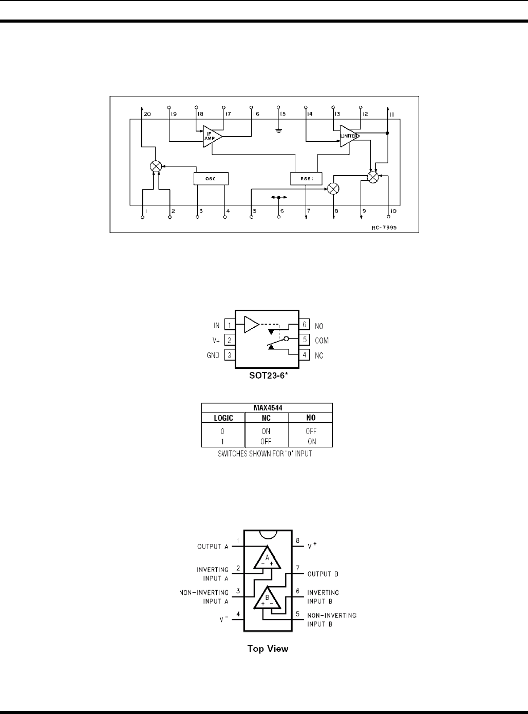
U101 19A705535P3 FM Receiver Module SA605: PHILIPS SEMI
U102
and
U103
RYT 101 6239/C Dual Analog Switch (SPDT) MAX4544: MAXIM
U104 GNLM239D Quad Operational Amplifier LM239A/SO: ON SEMI
U105 VELM6172IM Dual High Speed, Low Power, Low Distortion Voltage
Feedback Amplifier LM6172IM: NATIONAL SEMI
U106 GNLM239D Quad Operational Amplifier LM239A/SO: ON SEMI
U200 RYT 101 6140/2 Rail-To-Rail Operational Amplifier TLC2274/SO: TI
U201 19A704971P10 +8 Volt Regulator MC78M08C/TO
U202 10A704971P9 +5 Volt Regulator LM78L05AC/SO: FAIRCHILD SEMI
U203 RYT 101 6002/2C Low Power Quad Operation Amplifier LM2902/SO: ON
SEMI
U204 344A3064P201 3-To-8 Line Decoder/Demultiplexer 74HCT138/SO: ON
SEMI
U205 19A703483P311 CMOS Quad-Input OR Gate 74HC32/SO: ON SEMI
U206 19A703987P324 8-Bit Shift Register 74HC595/SO: ON SEMI
U207 RYT 101 6239/C Dual Analog Switch (SPST) MAX4544: MAXIM
MAX4544: MAXIM
U208 19A704971P10 +8 Volter Regulator MC78M08C/TO: ON SEMI
- - - - CRYSTALS - - - -
Y100 CY101062V1 20.945 MHz: TEN, NDK, Toyocom
Y101 19A149976P1 Discriminator: 455 kHz MURATA
105 PB101127V1 Receiver IF Printed Wiring Board
IC DATA
MM101886V1 R1A 23
7.0 IC DATA
U1, U104, U106
Quad Operational Amplifier
GNLM239/C (LM239A/SO)
U100
Automatic Gain Control (AGC) Amplifier
VEUPC3206GR-E1 (UPC3206GR)
Continued
IC DATA
24 MM101886V1 R1A
Continued
IC DATA
MM101886V1 R1A 25
U101
FM Receiver Module
19A705535P3
U102, U103, U207
Dual Analog Switch (Single-Pole/Double-Throw)
RYT 101 6239/C (MAX4544)
U105
Dual High Speed, Low Power, Low Distortion Voltage Feedback Amplifier
VELM6172IM (LM6172IM)
IC DATA
26 MM101886V1 R1A
U200
Rail–to-Rail Operational Amplifier
RYT 101 6140/2 (TLC2274/SO)
IC DATA
MM101886V1 R1A 27
U201, U208
+8 Volt Regulator
19A704971P10 (MC78M08C/TO)
U202
+5 Volt Regulator
19A704971P9 (LM78L05AC/SO)
Pinout:
1 - Vout
2 - Ground
3 - Ground
4 - N.C.
5 - N.C.
6 - Ground
7 - Ground
8 - Vin
IC DATA
28 MM101886V1 R1A
U203
Low Power Quad Operation Amplifier
RYT 101 6002/2C (LM2902/SO)
U204
3-8 Inverting Line Decoder/Demultiplexer
344A3064P201 (74HCT138/SO)m
IC DATA
MM101886V1 R1A 29
U205
Quad 2-Input OR Gate
19A703483P311 (74HC32/SO)
U206
8-Bit Shift Register
19A703987P324 (74HC595/SO)
OUTLINE DIAGRAM
30 MM101886V1 R1A
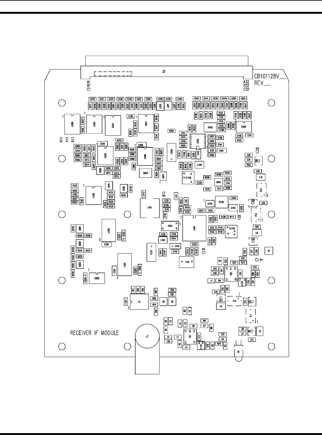
8.0 OUTLINE DIAGRAM
RECEIVER IF MODULE
CB101128V1
(AD-CB101128V1, Sh.3, Rev. B)
SCHEMATIC DIAGRAM
MM101886V1 R1A 31
9.0 SCHEMATIC DIAGRAM
RECEIVER IF MODULE
CB101128V1
(WD-CB101128V1, Sh. 1, Rev. A)
SCHEMATIC DIAGRAM
32 MM101886V1 R1A
RECEIVER IF MODULE
CB101128V1
(CB101128V1, Sh. 2, Rev. A)
SCHEMATIC DIAGRAM
MM101886V1 R1A 33
RECEIVER IF MODULE
CB101128V1
(CB101128V1, Sh. 3, Rev. A)

M/A-COM Wireless Systems
3315 Old Forest Road
Lynchburg, Virginia 24501
(Outside USA, 434-385-2400) Toll Free 800-528-7711
www.macom-wireless.com Printed in U.S.A.