HARRIS TR-0017-E Sitepro Base Station User Manual TX Synth
HARRIS CORPORATION Sitepro Base Station TX Synth
HARRIS >
Contents
TX Synth

Maintenance Manual
LBI-38640G
VHF TRANSMITTER SYNTHESIZER MODULE
19D902780G1
TABLE OF CONTENTS
Page
DESCRIPTION . . . . . . . . . . . . . . . . . . . . . . . . . . . . . . . . . . . . . . . . . . . . . . . Front Cover
GENERAL SPECIFICATIONS . . . . . . . . . . . . . . . . . . . . . . . . . . . . . . . . . . . . . . . . . 1
BLOCK DIAGRAM . . . . . . . . . . . . . . . . . . . . . . . . . . . . . . . . . . . . . . . . . . . . . . . 1
CIRCUIT ANALYSIS . . . . . . . . . . . . . . . . . . . . . . . . . . . . . . . . . . . . . . . . . . . . . . 1
VOLTAGE CONTROLLED OSCILLATOR . . . . . . . . . . . . . . . . . . . . . . . . . . . . 1
RF AMPLIFIERS . . . . . . . . . . . . . . . . . . . . . . . . . . . . . . . . . . . . . . . . . . . 1
REFERENCE BUFFER AMPLIFIER . . . . . . . . . . . . . . . . . . . . . . . . . . . . . . . . 2
PRESCALER AND SYNTHESIZER . . . . . . . . . . . . . . . . . . . . . . . . . . . . . . . . . 2
LOOP BUFFER AMPLIFIERS . . . . . . . . . . . . . . . . . . . . . . . . . . . . . . . . . . . . 2
AUDIO FREQUENCY AMPLIFIER . . . . . . . . . . . . . . . . . . . . . . . . . . . . . . . . . 2
VOLTAGE REGULATORS . . . . . . . . . . . . . . . . . . . . . . . . . . . . . . . . . . . . . . 2
LOGIC CIRCUITS . . . . . . . . . . . . . . . . . . . . . . . . . . . . . . . . . . . . . . . . . . 2
MAINTENANCE . . . . . . . . . . . . . . . . . . . . . . . . . . . . . . . . . . . . . . . . . . . . . . . . 2
TEST PROCEDURE . . . . . . . . . . . . . . . . . . . . . . . . . . . . . . . . . . . . . . . . . . 2
ALIGNMENT PROCEDURE . . . . . . . . . . . . . . . . . . . . . . . . . . . . . . . . . . . . . 3
TROUBLESHOOTING . . . . . . . . . . . . . . . . . . . . . . . . . . . . . . . . . . . . . . . . 3
OUTLINE DIAGRAM . . . . . . . . . . . . . . . . . . . . . . . . . . . . . . . . . . . . . . . . . . . . . . 4
ASSEMBLY DIAGRAM . . . . . . . . . . . . . . . . . . . . . . . . . . . . . . . . . . . . . . . . . . . . . 5
SCHEMATIC DIAGRAM . . . . . . . . . . . . . . . . . . . . . . . . . . . . . . . . . . . . . . . . . . . . 6
PARTS LIST . . . . . . . . . . . . . . . . . . . . . . . . . . . . . . . . . . . . . . . . . . . . . . . . . . . . 9
PRODUCTION CHANGES . . . . . . . . . . . . . . . . . . . . . . . . . . . . . . . . . . . . . . . . . . . 10
IC DATA . . . . . . . . . . . . . . . . . . . . . . . . . . . . . . . . . . . . . . . . . . . . . . . . . . . . . 11
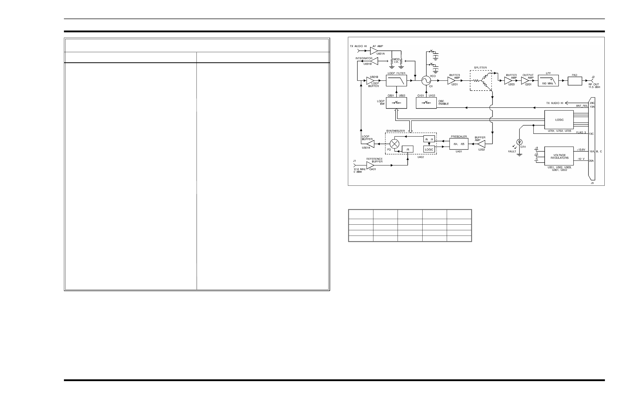
DESCRIPTION
The principle function of the Transmitter Synthesizer
Module is to provide the RF excitation for input to the
MASTR III station power amplifier. The output of the syn-
thesizer is a frequency modulated signal at the desired fre-
quency. The module contains the following functional
blocks:
•A voltage controlled oscillator.
•A chain of integrated circuit RF Amplifiers.
•A reference buffer amplifier.
•Dual modulus prescaler and synthesizer integrated
circuits.
•Loop amplifiers and passive loop filter.
•An audio amplifier and a pre-modulation integrator.
•IC voltage regulators for +5 and -5 Vdc. A discrete
component regulator for +8 Vdc, and an Opera-
tional Amplifier regulator for +4 Vdc.
•Logic circuitry: address decoder, input signal gates,
and a lock indicator circuit.
M/A-COM Wireless Systems
3315 Old Forest Road
Lynchburg, Virginia 24501
(Outside USA, 434-385-2400) Toll Free 800-528-7711
www.macom-wireless.com Printed in U.S.A.
Copyright © 1992-2002, M/A-COM Private Radio Systems, Inc. All rights reserved.
Table 1 - General Specifications
ITEM SPECIFICATION
FREQUENCY RANGE 136 to 174 MHz
in 4 bands 136 to 144 MHz
142 to 152 MHz
150 to 162 MHz
160 to 174MHz
RF POWER OUT(50 Ohm load) 10 to 13 dBm
(10 to 20 mW)
RF HARMONICS <-30 dBc
NON-HARMONIC SPURS
1 to 200 MHz <-90 dBc
200 MHz to 1 GHz <-60 dBc
CARRIER ATTACK TIME <50 ms
REFERENCE INPUT
input level 0 dBm ±1.5dB
input impedance 50 Ohm
frequency 5 to 17.925 MHz (must be integer divisible by
channel spacing)
MODULATION SENSITIVITY 5 kHz peak dev/1 Vrms
AF INPUT IMPEDANCE 600 Ohm
AF RESPONSE
10 Hz ±1.5 dB
1000 Hz 0 dB reference
3 kHz ±1.5 dB
10 Hz SQUARE WAVE MODULATION <10%
Sq wave droop
HUM & NOISE -55 dB
POWER REQUIREMENTS 13.8 Vdc @ 275 mA
-12.0 Vdc@ 10 mA
CIRCUIT ANALYSIS
VOLTAGE CONTROLLED OSCILLATOR
Transistor Q1 and associated circuitry comprise a low noise
Voltage Controlled Oscillator (VCO). Inductor L1 and associ-
ated capacitors form the oscillator resonant circuit (tank). The
noise characteristic of this oscillator is dependent on the Q of
this resonant circuit. The components used in the tank are
specified to have especially high Q. Diode D1 aids in setting
the bias point for low noise operation. (Any field replacement
of oscillator parts should use identical parts).
Switches SWIA, SWIB, SWIC and SWID set the fixed
capacitance in the tank and therefore set the frequency range
over which the oscillator can be voltage tuned. Table 2 shows
the switch settings for the various frequency ranges.
Switches SW1E (SW#5) and SW1F (SW#6) also set the
fixed capacitance in the tank and perform the frequency
trimming function. These two switches are factory set and
should not need resetting unless any oscillator components
are changed. (See alignment procedure section of this man-
ual for instructions on resetting SW1E and SW1F).
The oscillator frequency is voltage tuned by the signal
applied through R5 and L5 to the two varicap diodes D2 and
D3. Additionally, audio modulation is applied as an AF
voltage to the two varicap diodes. This AF voltage varies the
oscillator frequency at an audio rate (i.e., it frequency modu-
lates the oscillator). Low frequency audio is applied along
with the varicap control voltage through R5 and L5 while
high frequency audio (MOD) is applied via C16.
Resistors R6 through R9 provide a two volt negative bias
on the varicap diodes.
Figure 1 - Block Diagram
Transistors Q101 and Q102 and associated circuitry form
the oscillator enable switch. This switch allows the station
control circuitry to turn the VCO ON or OFF via the
ANT_REL line. Setting the ANT_REL line to a logic low
causes Q102 to conduct. The five (5) volt output at Q102
collector (OSCON) enables the fault indicator gates, U705C
and U705D, and turns on Q101. Q101 starts to conduct,
providing a ground path for Q1. This turns ON the VCO.
RF AMPLIFIERS
Integrated circuits U201 and U202 and U203 and tran-
sistor Q201 form a chain of RF amplifiers. These amplifiers
serve two purposes; amplifying the RF signal for input to the
power amplifier and providing a signal to the Phase-Locked
Loop (PLL) .
Integrated circuits U201, U203 and transistor Q201
provide amplification for the RF signal which will be fed to
the station power amplifier. U201 operates with a gain of
about 5 dB. Its output is fed to a resistive signal splitter
composed of R203 through R210.
One of the resistive signal splitter outputs drives U203.
U203 operates with a gain of about 10 dB. Q201 and associ-
ated circuitry comprise the output amplifier which has a gain
of about 6 dB. This amplifier is followed by a 190 MHz
cutoff low -pass filter (C216, C217, L203 and L204) and a 6
dB resistive attenuator (R219 through R221). The final out-
put at the front panel BNC connector (J2) is nominally 11.5
dBm into a 50 ohm load.
Table 2 - Frequency Range Switch Settings
FREQUENCY
RANGE (MHz) SW1A
(SW#1) SW1B
(SW#2) SW1C
(SW#3) SW1D
(SW#4)
160-174 OPEN OPEN OPEN OPEN
150-162 CLOSED OPEN CLOSED OPEN
142-152 OPEN CLOSED OPEN CLOSED
136-143 CLOSED CLOSED CLOSED CLOSED
LBI-38640G
1

The other output of the resistive splitter drives U202.
U202 is a buffer amplifier with a gain of about 10 dB. U202
drives the synthesizer prescaler (i.e. it provides a signal to
the PLL).
REFERENCE BUFFER AMPLIFIER
Transistor Q401 and associated components comprise a
buffer amplifier for the reference oscillator signal. (The
reference oscillator signal is produced by the receiver syn-
thesizer module of a MASTR III station.) The 0 dBm refer-
ence oscillator signal is fed through the front panel BNC
connector J1. Resistor R405 provides a 50 ohm load to the
reference oscillator. The output of the Reference Buffer
Amplifier is fed directly to the synthesizer integrated circuit.
The output level at TP9 is approximately 3 volts peak to
peak.
PRESCALER AND SYNTHESIZER
Integrated circuit U402 is the heart of the synthesizer. It
contains the necessary frequency dividers and control cir-
cuitry to synthesize output frequencies by the technique of
dual modulus prescaling. U402 also contains an analog
sample and hold phase detector and a lock detector circuit.
Within the synthesizer (U402) are three programmable
dividers which are loaded serially using the CLOCK, DATA,
and ENABLE inputs (pins 11, 12, and 13 respectively). A
serial data stream (DATA) on pin 12 is shifted into internal
shift registers by low to high transitions on the clock input
(CLOCK) at pin 11. A logic high (ENABLE) on pin 13 then
transfers the program information from the shift registers to
the divider latches.
The reference signal is applied to U402 pin 2 and divided
by the "R" divider. This divides the reference signal down to
a divided reference frequency (Fr). The typical reference
frequency is 12.8 MHz and the typical divided reference
frequency is 5 kHz providing for synthesizer steps of 5 kHz
for use with both 25 kHz and 30 kHz channel spacing. Other
channel spacings are possible by providing proper program-
ming.
The "A" and "N" dividers process the loop feedback
signal provided by the VCO (by way of the dual modulus
prescaler U401). The output of the "N" divider is a divided
version of the VCO output frequency (Fv).
Synthesizer U402 also contains logic circuitry to control
the dual modulus prescaler U401. If the locked synthesizer
output frequency is 150 MHz. The prescaler output nomi-
nally will be equal to 2.34375 MHz (150 MHz/64). This
frequency is further divided down to Fv by the "N" divider
in U402. Fv is then compared with Fr in the phase detector
section.
The phase detector output voltage is proportional to the
phase difference between Fv and Fr. This phase detector
output serves as the loop error signal. This error signal
voltage tunes the VCO to whatever frequency is required to
keep Fv and Fr locked (in phase).
LOOP BUFFER AMPLIFIERS AND LOOP
FILTER
The error signal provided by the phase detector output is
buffered by operational amplifiers (op-amp) U501A and
U501B. The audio modulation signal from U601B is also
applied to the input of U501B. The output of U501B is the
sum of the audio modulation and the buffered error signal.
The output of the second buffer (U501B) is applied to a
loop filter consisting of R506, R507, R508, C505 and C506.
This filter controls the bandwidth and stability of the synthe-
sizer loop. The VHF transmitter synthesizer has a loop
bandwidth of only several Hertz. This is very narrow, result-
ing in an excessively long loop acquisition time. To speed
acquisition, switches U502A and U502C bypass the filter
circuit whenever an ENABLE pulse is received by the Input
Gates.
AUDIO FREQUENCY AMPLIFIER
The transmitter synthesizer audio input line is fed to
U601A. U601A is configured as a unity gain op-amp. Resis-
tor R601 sets the 600 ohm input impedance of this amplifier.
(NOTE: Data for digital modulation is fed to the synthesizer
through the audio input line).
The amplifier output is split into two components and fed
to two variable resistors VR601 and VR602. VR601 sets the
level in the low frequency audio path and VR602 sets the
level in the high frequency audio path. (There is no clear
break between the low and high frequency ranges. All voice
frequencies are within the high frequency range. The low
frequency range contains low frequency data components).
The wiper of VR601 (low frequency path) connects to
the input of U601B, the pre-modulation integrator. U601B
performs the function of a low-pass filter and integrator. The
integrator output is summed with the PLL control voltage at
the input of loop buffer amplifier U501B. This integrated
audio signal phase modulates the VCO. The combination of
pre- integration and phase modulation is equivalent to fre-
quency modulation.
The wiper of VR602 (high frequency path) is connected
to the modulation input of the VCO through C16.
VOLTAGE REGULATORS
U301 and U303 are monolithic voltage regulators (+5
Vdc and -5 Vdc respectively). These two voltages are used
by synthesizer circuitry. The +5 V regulator output is also
used as a voltage reference for the +8 Vdc discrete regulator
circuit.
U302A, Q302 and associated circuitry comprise the +8 volt
regulator. Most module circuitry is powered from the +8 volt
line. The regulator is optimized for especially low noise per-
formance. This is critical because the low noise VCO is pow-
ered by the +8 volt line.
The +8 Vdc line also feeds the +4 Vdc regulator, U302B
and associated resistors. The +4 Vdc regulator provides a bias
voltage for several op-amps in the module.
LOGIC CIRCUITS
Logic circuitry (other than that inside the synthesizer IC -
U402) consists of the following:
•An address decoder
•Input gates and level shifters
•Lock Indicator circuitry
The address decoder, U702, enables the Input Gates when
the A0, A1, and A2 input lines receive the proper logic code
(110 for the transmitter synthesizer). After receiving the proper
code, Y3 (U702-12) sends a logic low signal to U701C. U701C
acts as an inverter and uses the logic high output to turn on
Input Gates U701A, U701B, and U701D. The Input Gates
allow the clock, data and enable information to pass on to the
synthesizer via the level shifters. The Level Shifter Transistors
Q701, Q702 and Q703 convert the 5 volt gate logic level to the
8 volt logic level required by the synthesizer U402.
The Fault Indicator circuitry indicates when the synthe-
sizer is in an out-of-lock condition. The fault detector latches,
U705A and U705B are reset by the enable pulse during initial
loading of data into the synthesizer. If at any time afterwards
the lock detector signal (LD) goes low, the high output of
U705B will cause the output of gates U705C and U705D to go
low. The low output from U705C causes Q704 to turn off, thus
turning on the front panel LED (CR701). The output of U705D
(FLAG) i s connected to J3-13C for external monitoring of the
Synthesizer Module. A logic low on the FLAG line indicates
an out-of-lock condition.
MAINTENANCE
RECOMMENDED TEST EQUIPMENT
The following test equipment is required to test the synthe-
sizer Module:
1. RF signal source for 12.8 MHz, 0 dBm reference (in-
cluded with item 10)
2. AF Generator or Function Generator
3. Modulation Analyzer; HP 8901A, or equivalent, or a
VHF receiver
4. Oscilloscope; 20 MHz
5. DC Meter; 10 meg ohm (for troubleshooting)
6. Power Supply;13.8 Vdc @ 350 mA 12.0 Vdc @ 25
mA
7. Spectrum Analyzer; 0-1 GHz
8. Frequency Counter; 10 MHz - 250 MHz
9. Personal Computer (IBM PC compatible) to load fre-
quency data
10.Service Parts Kit, (TQ0650), (includes software for
loading frequency data)
TEST PROCEDURE
(Steps 5, 6, and 7 can be done using a modulation analyzer
or VHF receiver with 750us de-emphasis switchable in or out.
1. Program synthesizer at 167.5 MHz using the System
Module personality (or Test Software if using RF
Test Fixture TQ-0650).
Verify lock (flag = high)
Verify front panel LED is off.
2. Measure output frequency.
Verify frequency = 167.5000 MHz ±100 Hz.
3. Measure harmonic content (335 MHz, 502.5MHz).
Verify 2nd harmonic is 30 dBc.
4. Measure RF power output into 50 ohm load.
Verify 10 to 13 dBm (10 to 20 mW).
5. Measure AF distortion with standard modulating sig-
nal input.
Verify <5%.
6. Measure Hum and Noise relative to 0.44 kHz average
deviation, (de-emphasis on).
Verify <-55dB
7. Measure AF response at 300 Hz, 1 kHz (ref) and 3
kHz, (de-emphasis off).
Verify within ±1.5 dB with respect to 1 kHz refer-
ence.
8. Verify lock at different frequencies.
a. Close switches SW1A and SW1C.
b. Program synthesizer at 156 MHz.
Verify LED is off.
LBI-38640G
2
c. Open switches SW1A and SW1C and close
switches SW1B and SW1D.
d. Program synthesizer at 147 MHz.
Verify LED is off.
e. Close switches SW1A, SW1B, SW1C and
SW1D.
f. Program synthesizer at 139.5 MHz.
Verify LED is off.
g. Open switches SW1A, SW1B, SW1C and
SW1D.
ALIGNMENT PROCEDURE
1. Set all sections of SW1 to the open position.
2. Apply +13.8 Vdc and -12 Vdc. Verify the current
drain on the 13.8 volt supply is <300 mA and the cur-
rent drain on the -12 volt supply is <20 mA.
3. Program the synthesizer at 175 MHz. Set SW1E and
SW1F (4 possible Combinations = both closed, both
open, E open and F closed, or E closed and F open)
to set Vtest (pin 23A of 96 pin connector) as close to
6.0 volts as possible, but always between 5.5 and 6.5
volts.
4. Program synthesizer at 167.5 MHz for the following
three adjustments
•Set VR602 for 4.5 kHz peak deviation with a standard
modulating signal applied to the audio input.
•Set VR601 for 4.4 kHz peak deviation with 1.0 Vrms,
10 Hz sine wave audio applied to module AF input.
•Apply a 10 Hz 1.4 Vpk square wave (same peak value
as 1.0 Vrms (sine wave) to module AF input. Adjust
VR601 slightly for the flattest demodulated square
wave using a modulation analyzer or receiver (no de-
emphasis) and an oscilloscope . The maximum net
variation in voltage over 1/2 cycle is 10%.
The following service information applies when align-
ing, testing, or troubleshooting the TX Synthesizer:
•Standard Modulating Signal = 1 kHz sinusoidal
voltage, 1.0 Vrms at the module input terminals
(600 ohm Rin).
•The input audio level for setting the 4.5 kHz or 10
Hz (or 7 Hz) deviation should always be 1.00
Vrms.
•In the modulation adjustment, any reference to 0.6
Vrms refers to the voltage level for a STANDARD
signal, or usually 60% (3.0 kHz) of maximum
deviation. The 0.6 Vrms will produce 60% of full
deviation.
•Logic Levels:
Logic 1 = high = 4.5 to 5.5 Vdc
Logic 0 = Low = 0 to 0.5 Vdc
•Transmitter Synthesizer Address = A0 A1 A2
= 110
•Synthesizer data input stream is as follows:
14-bit "R" divider most significant bit (MSB) =
R13 through "R" divider least significant bit
(LSB) = R0
10-bit "N" divider MSB = N9 through "N" divider
LSB = N0
7-bit "A" divider MSB = A6 through "A" divider
LSB = A0
Single high Control bit (last bit)
Latched When Control Bit = 1
DATA ENTRY FORMAT
Latched When
Control Bit = 1
Data in Last A0 ---- A6 N0 ---- N9 R0 ---- R13
Bit LSB MSB LSB MSB LSB
Control Bit
For the transmitter synthesizer, 5 kHz channel
spacing
R=2560
N = integer part of (frequency in kHz) / (320)
A = (frequency in kHz)/(5) - 64*N
All numbers must be converted to binary.
•ANT_REL line must be logic low (0V) in order to
lock synthesizer.
•Synthesizer lock is indicated by the extinguishing
of the front panel LED indicator and a logic high
on the fault flag line (J3 pin 1 3C).
•Always verify synthesizer lock after each new data
loading.
SYMPTOM CHECK INCORRECT READING
(CORRECT READINGS SHOWN) INDICATES DEFECTIVE COMPONENT
SYNTHESIZER FAILS TO LOCK Check DC voltages
+5 V @ U301 Pin 1 U301 or associated components
+8 V @ Q301 collector U302, Q301, Q302 or associated components
- 5 V @ U303 Pin 1 U303 or associated components
Check 12.8 MHz reference signal No reference signal to front panel BNC or
3V P-P, 12.8 MHz @ TP9 or U402 Pin 2 Q401
Check oscillator signal
11.5 1.5 dBm 125 to 180 MHz at Proceed to "Low/No RF output" below
front panel BNC
Check prescaler output
1V P-P, 2.5 MHz @ U401 Pin 4 U202, U401
Check CLOCK, DATA, ENABLE
While loading frequency data into Wrong address or
synthesizer Check 8V logic signals @ U701, U702, Q701, Q702, Q703
Pins 11, 12, 13 of U402
Check Phase detector output
5 kHz random signal @ U501 Pin 7 U402, U501
Low/No RF Output Check oscillator
LESS than 0.5 Vdc @ TP3 or collector Synthesizer not keyed (low on ANT relay line)
of Q101 or Q101, Q102
50 mV, 125 to 180 MHz @ TP4 Q1
No Modulation Check RF chain
0 dBm, 125 to 180 MHz @ TP6 U201
+5 dBm, 125 to 180 MHz @ TP7 U203
11.5 ±1.5 dBm to 180 MHz at front Q201
panel BNC
No Modulation Check AF amplifier
Apply 1V, 1 kHz signal to TX/Audio/ Hi U601
Check 1V signal @ TP12 or U601 Pin 1
TROUBLESHOOTING GUIDE
TROUBLESHOOTING
A troubleshooting guide is provided showing typical
measurements at the various test points. The location of the
test points and adjustments are shown in Figure 2.
Perform step 3 only if switch SW1 has been replaced.
Otherwise go to step 4.
NOTE
SERVICE NOTES
LBI-38640G
3
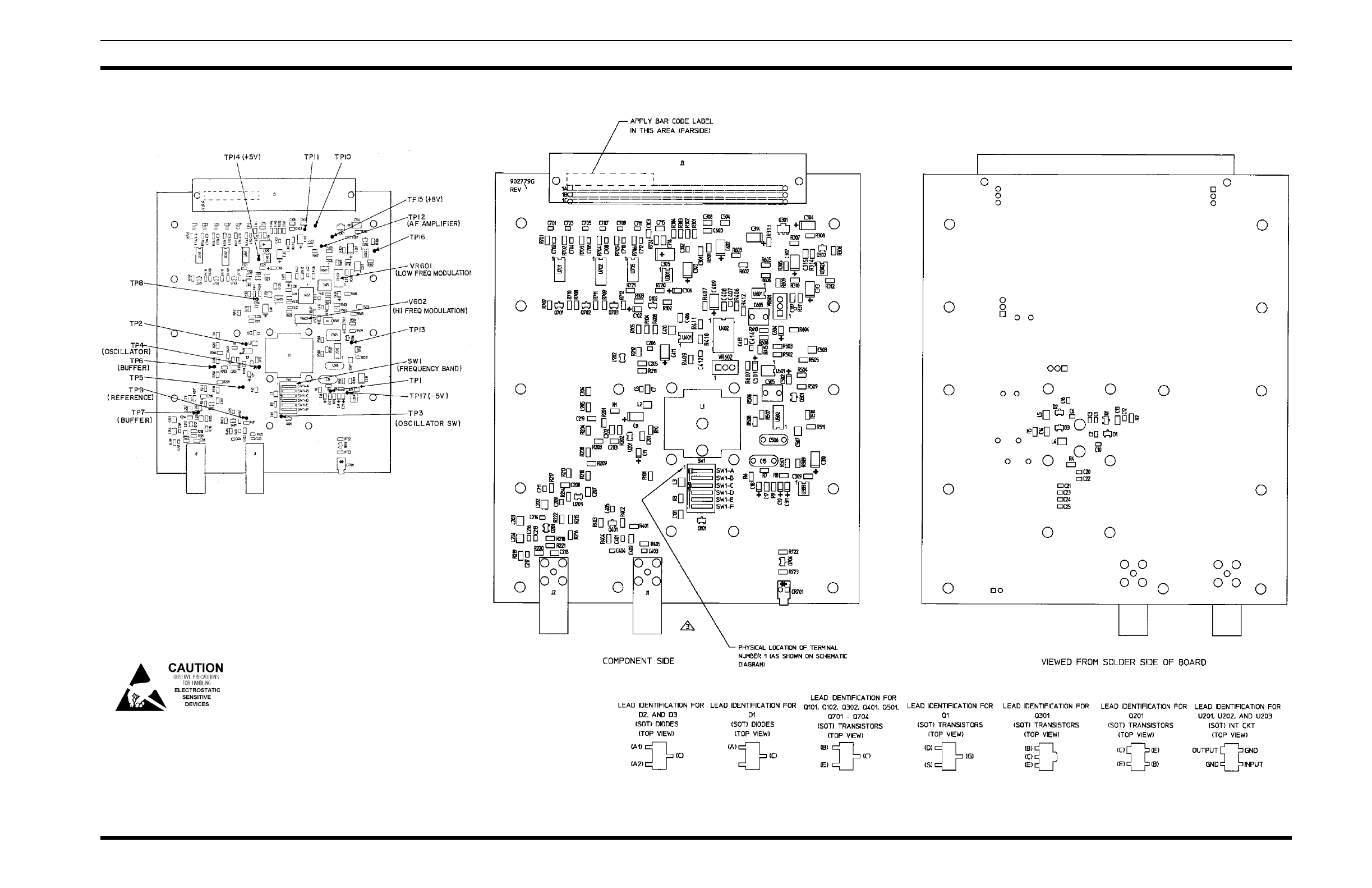
OUTLINE DIAGRAM
VHF TRANSMITTER
SYNTHESIZER BOARD
19D902779G1
(19D902779, Sh. 1, Rev. 13)
Figure 2 - Test Point Locations
LBI-38640G
4
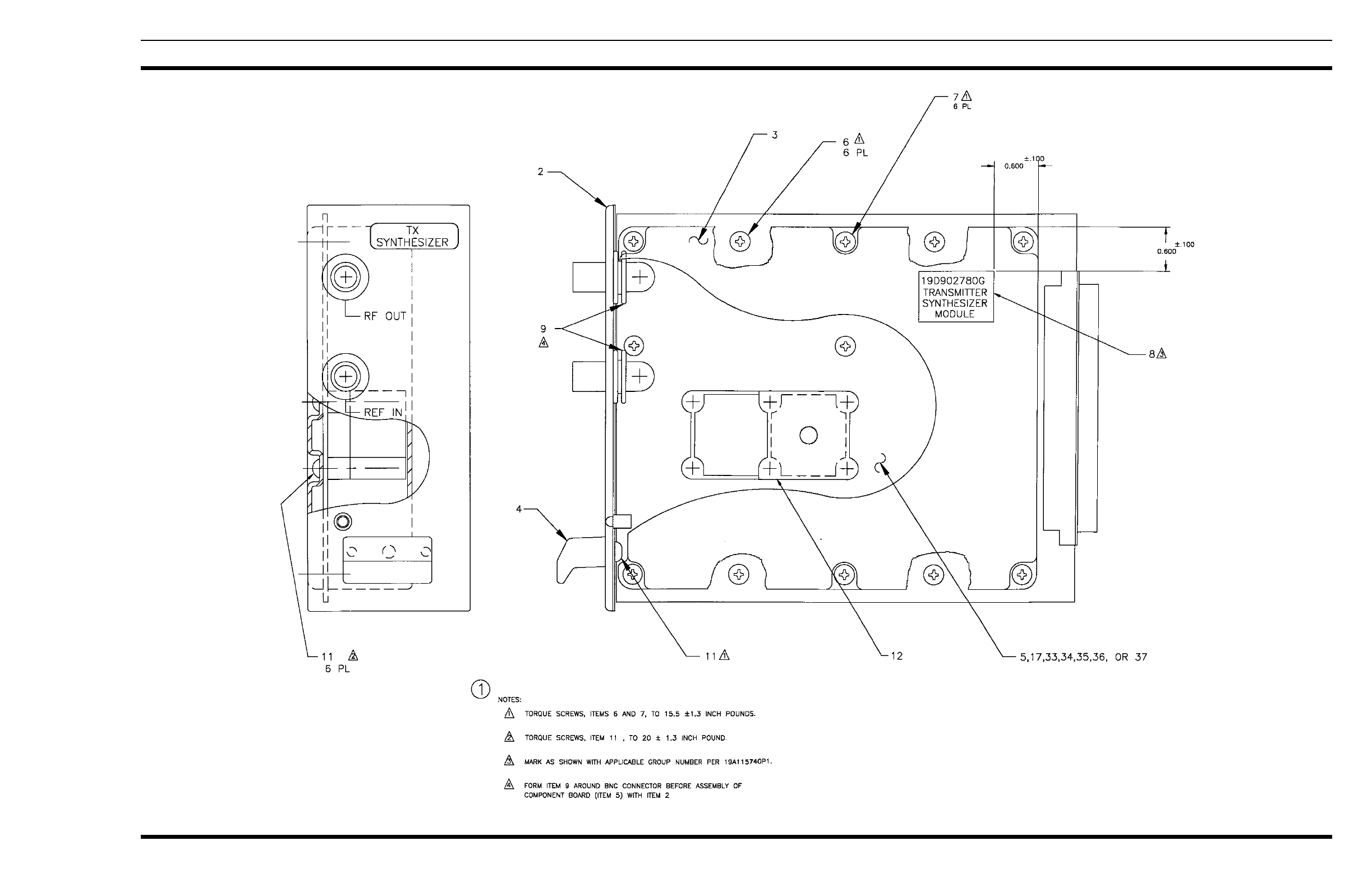
ASSEMBLY DIAGRAM
VHF TRANSMITTER SYNTHESIZER MODULE
19D902780G1
(19D902780, Sh. 1, Rev. 7)
LBI-38640G
5
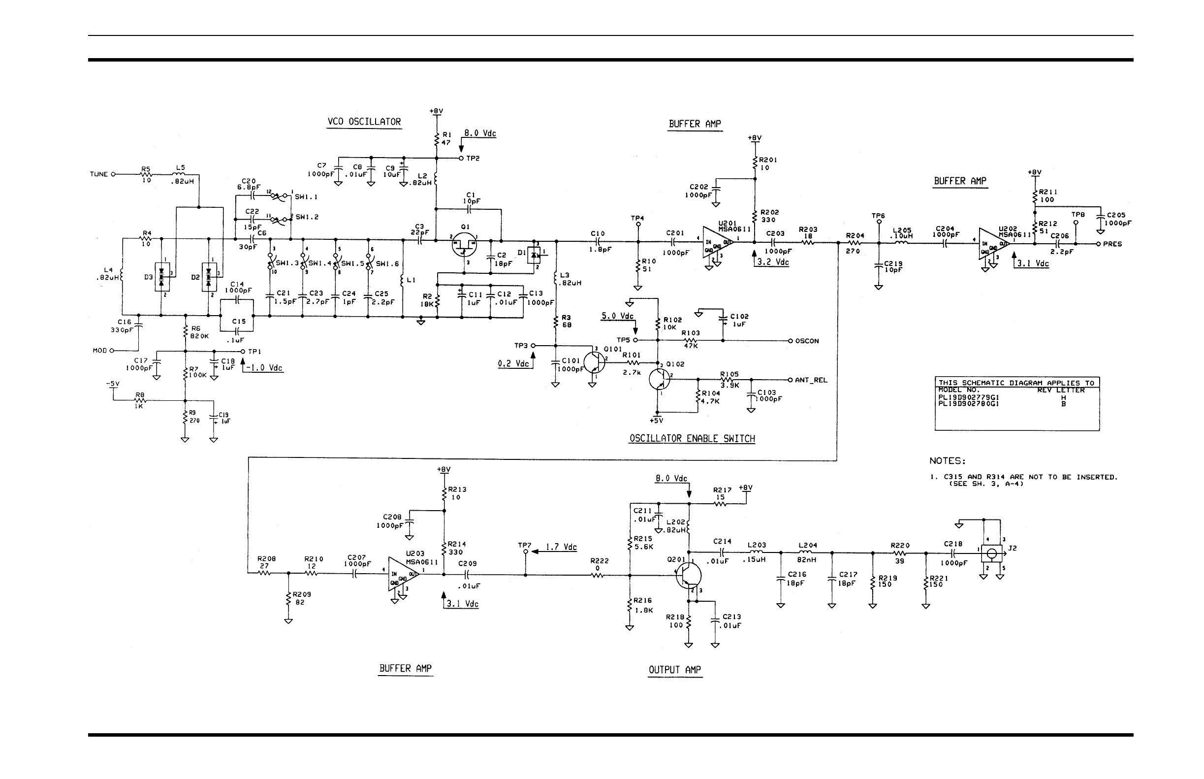
SCHEMATIC DIAGRAM
VHF TRANSMITTER SYNTHESIZER
19D902780G1
(19D902622 Sh. 1, Rev. 12)
LBI-38640G
6
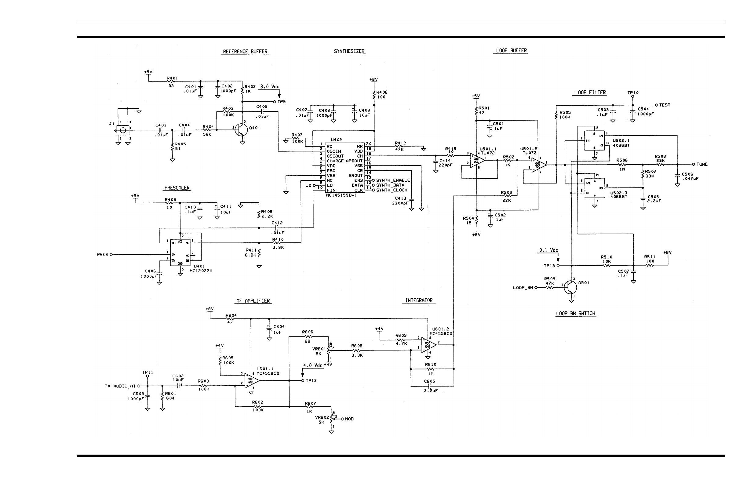
SCHEMATIC DIAGRAM
VHF TRANSMITTER SYNTHESIZER
19D902780G1
(19D902622, Sh. 2,Rev. 12)
LBI-38640G
7
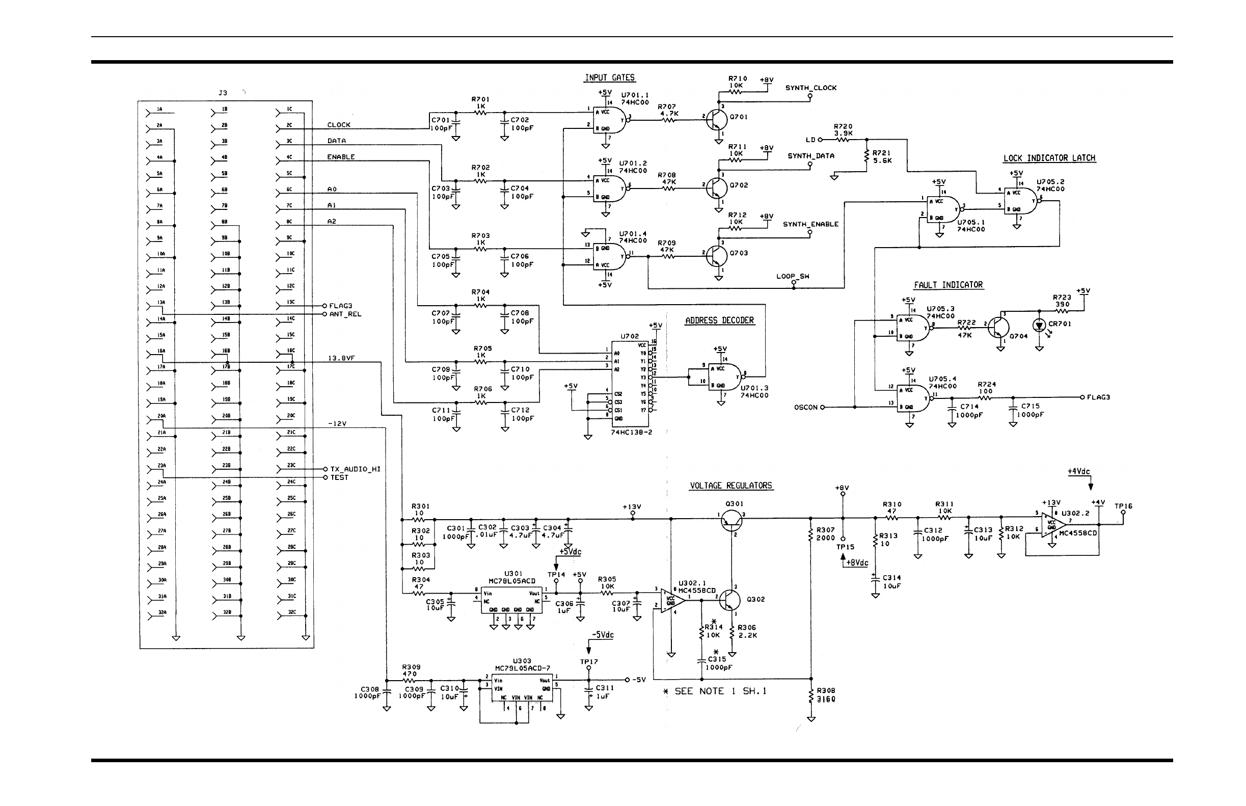
SCHEMATIC DIAGRAM
VHF TRANSMITTER SYNTHESIZER
19D902780G1
(19D902622, Sh. 3, Rev. 12)
LBI-38640G
8
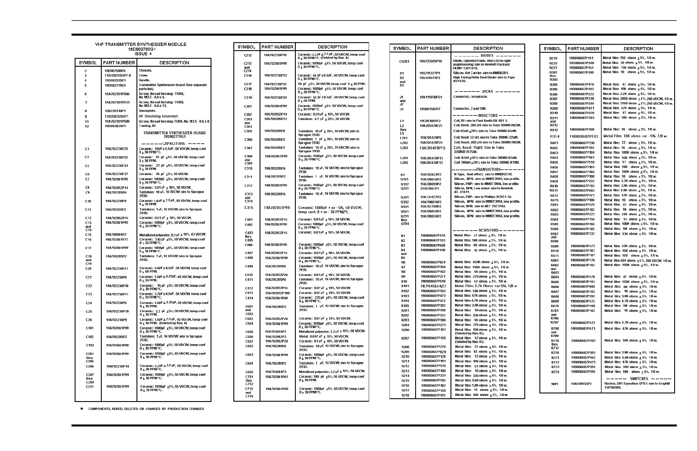
PARTS LIST LBI-38640G
9
PARTS LIST & PRODUCTION CHANGES
PRODUCTION CHANGES
Changes to the equipment to improve performance or to simplify
circuits are identified by a Revision Letter which is stamped after the
model number of the unit. The revision stamped on the unit includes
all previous revisions. Refer to the partls List for the descriptions of
parts affected by this revision.
Rev. A - Transmitter Synthsizer Board - 19D902779G1
To improve reliability, changed C21, C23, C24, C25, C216,
C305, L203, L204, R211, R219, R220 and R221. Deleted
C26 and C212 and added C217.
C21 was: 19A702236P11, 2.7 pF.
C23 was: 19A702236P19, 5.6 pF.
C24 was: 19A702236P9, 1.8 pF.
C25 was: 19A702236P13, 3.3 pF.
C216 was: 19A702236P21, 6.8 pF.
C305 was: 19A705205P6, 10 µH.
L203 was: 19A705470P18, 0.27 µH.
L204 was: 19A705470P13, 0.10 µH.
R211 was: 19B800607P100, 10 ohms.
R219 was: 19B800607P221, 220 ohms.
R220 was: 19B800607P270, 27 ohms.
R221 was: 19B800607P221, 220 ohms.
Rev. B - Transmitter Synthsizer Board - 19D9027791
To improve Lock-on at low end of board and to improve
stabilization of +8 volt power supply. Changed C312, R204
and R310; replaced R206 with C219 and R207 with L205.
C312 was: 19A702061P99, 1000 pF.
R204 was: 19B80607P270, 27 ohms.
Rev. C - Transmitter Synthsizer Board - 19D902779G1
To improve the margin of stability on the +8 Vdc power
supply, changed C312 and R310, and added C314 and
R313.
C312 was: 19A705205P2, 1 µF.
R310 was: 19B800607P100, 10 ohms.
Rev. D - Transmitter Synthsizer Board - 19D902779G1
To correct loading problem.
R209 was: 100 ohms (19B801486P101).
R411 was: 4.7k ohms (19B800607P472).
R707 was 47k ohms (19B800607P473).
REV. E - Transmitter Synthesizer Board - 19D902779G1
To accommodate SOG synthesizer IC package U402 (PLCC
package discontinued). Modified printed wire board layout
(Printed wire board changed from 19D902644P1R5 to
19D902644P1R6). Added new U402. U402 was
19B800902P5. Installed RC compensation network resistor
R314 and capacitor C315 in 10-volt regulator circuit. In-
stalled item 9 RF shielding grommets (19B802690P1) on
two BNC connectors of input/output RF ports.
REV. A - Transmitter Synthesizer Module 19D902780G1
To install RF shielding grommets. Installed item 9 RF shield-
ing grommets (19B802690P1) on two BNC connectors of
input/output RF ports.
REV. F - Transmitter Synthesizer Board - 19D902779G1
To improve marginal power output at the high end of the VHF
Band (174 MHz). Changed inductor L203 from 0.18 µH
(19A705470P16) to 0.15µH. Changed resistor R220 from
39 ohms (19B800607P390) to 22 ohms. Inductor L203 was
a 19A705470P16. Resistor R220 was a 19B800607P390.
REV. B - Transmitter Synthesizer Module 19D902780G1
To install a cover that has a conductive gasket. Changed
item 3. Item 3 was a 1919D902509P2.
REV. G - Transmitter Synthesizer Board 19D902779G1
To increase the base current of transistor Q101 and ensure
saturation during turn on. Changed resistor R101. Resistor
R101 was 19B800607P473, 47k Ohms.
REV. H - Transmitter Synthesizer Board 19D902779G1
To decrease the output power by approximately 1.0 dB.
Changed resistor R220. Resistor R220 was
19B800607P220, 22 Ohms.
LBI-38640G
10
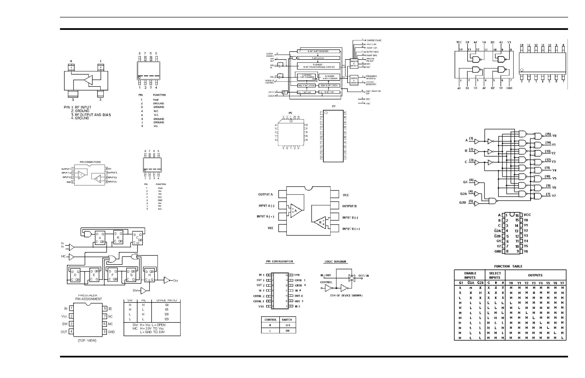
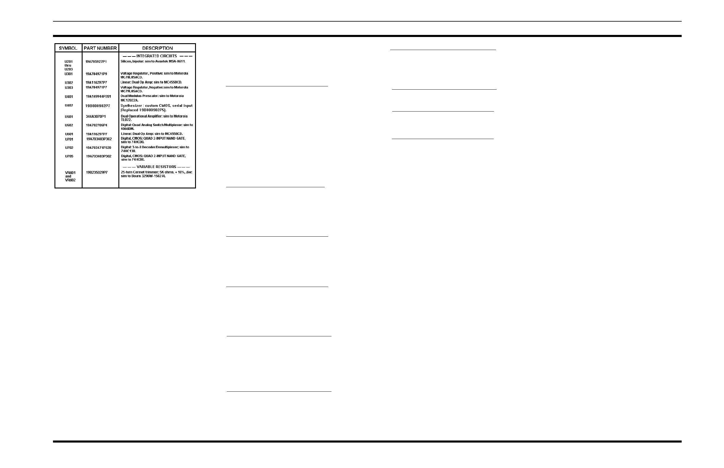
IC DATA
U302 & U601
19A116297P7
Dual Wide Band Op-Amp
U401
19A149944P201
Dual Modulus Prescaler
U501
344A3070P1
Operational Amplifier
U502
19A702705P4
Quad Analog Switch
U702
19A703471P320
Address Decoder
U701 & U705
19A703483P302
Quad 2-Input NAND Gate
U201 & U203
19A705927P11
Silicon Bipolar MMIC
U301
19A704971P9
+5V Regulator
U303
19A704971P7
-5V Regulator
U402
19B800902P5/P7
Synthesizer
LBI-38640G
11