HARRIS TR-0017-E Sitepro Base Station User Manual RX Synth
HARRIS CORPORATION Sitepro Base Station RX Synth
HARRIS >
Contents
RX Synth
Maintenance Manual
LBI-38641F
VHF RECEIVER SYNTHESIZER MODULE
19D902781G1 & G2
DESCRIPTION
The Receiver Synthesizer Module provides the local
oscillator signal (LO) to the Receiver Front End Module
of the MASTR III base station. The module also provides
the reference oscillator signal to the transmitter synthe-
sizer. Receiver Synthesizer Module 19D902781G1
(Group 1) generates an output injection signal in the 157
to 172 MHz range, and 19D902781G2 (Group 2) gener-
ates a signal in the 129 to 152 MHz Range.
The Receiver Synthesizer Module is a phase-locked
loop (PLL) design, as shown in the block diagram (Figure
1). Its output is generated directly by the VCO Q1 and
buffered by Monolithic Microwave Integrated Circuits
(MMIC) U1 and U3.
The logic signals from controller (U10, 12, and 13)
determine the synthesizer frequency. Frequency stability
is maintained by either using the internal reference oscil-
lator Y1 or by applying a high precision reference signal
to the EXT Reference Oscillator Port J4. The internal
reference oscillator is a temperature controlled crystal
oscillator (TCXO) operating at 12.8 MHz. The oscillator
has a stability of ±1.5 ppm over the temperature range of
-30°C to +75°C. See the table containing General Speci-
fications for the minimum external oscillator specifica-
tions.
The buffered VCO output is sampled by the resistive
splitter and conditioned by buffer amplifier U2. It is then
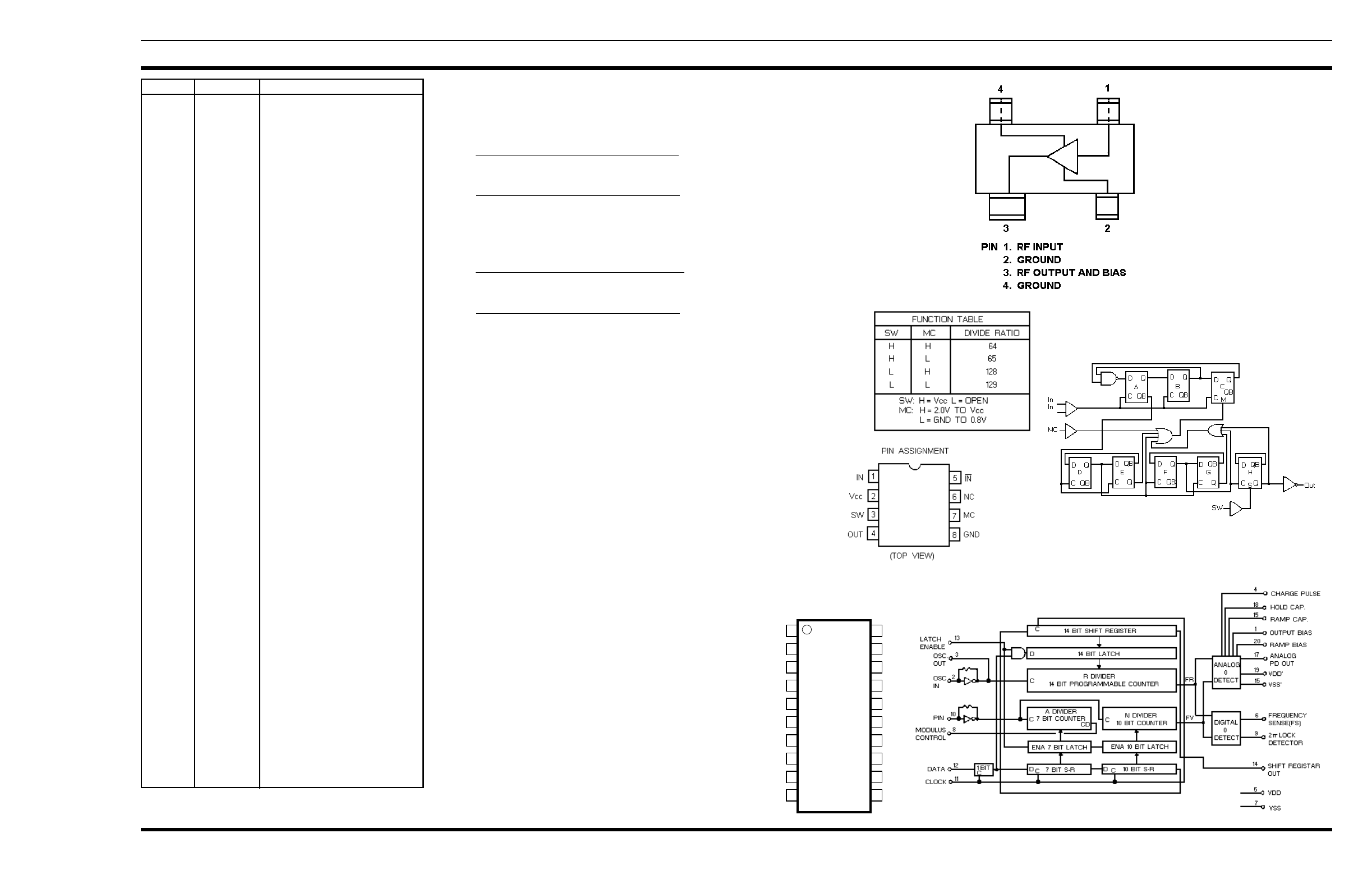
fed to the divide by 64/65 dual modulus prescaler U5. The
divided output from the prescaler is connected to the Fin
input of the PLL U6. Within the PLL the divided VCO
input signal Fin is divided again. The PLL also divides
down the 12.8 MHz reference signal. Three inputs from
the controller; ENABLE, CLOCK, and serial DATA pro-
gram the PLL divider circuits.
TABLE OF CONTENTS
Page
DESCRIPTION . . . . . . . . . . . . . . . . . . . . . . . . . . . . . . . . . . . . . . . . . . . . Front Cover
GENERAL SPECIFICATIONS . . . . . . . . . . . . . . . . . . . . . . . . . . . . . . . . . . . . . 1
CIRCUIT ANALYSIS . . . . . . . . . . . . . . . . . . . . . . . . . . . . . . . . . . . . . . . . . . 2
VOLTAGE CONTROLLED OSCILLATOR . . . . . . . . . . . . . . . . . . . . . . . . . . . . 2
BUFFER AMPLIFIERS . . . . . . . . . . . . . . . . . . . . . . . . . . . . . . . . . . . . . . . 2
REFERENCE OSCILLATOR AND BUFFER . . . . . . . . . . . . . . . . . . . . . . . . . . . 2
PRESCALER AND SYNTHESIZER . . . . . . . . . . . . . . . . . . . . . . . . . . . . . . . . 2
LOOP FILTER . . . . . . . . . . . . . . . . . . . . . . . . . . . . . . . . . . . . . . . . . . . . 2
DIGITAL CONTROL . . . . . . . . . . . . . . . . . . . . . . . . . . . . . . . . . . . . . . . . 2
VOLTAGE REGULATORS . . . . . . . . . . . . . . . . . . . . . . . . . . . . . . . . . . . . . 2
MAINTENANCE . . . . . . . . . . . . . . . . . . . . . . . . . . . . . . . . . . . . . . . . . . . . . 3
TEST AND ALIGNMENT PROCEDURE . . . . . . . . . . . . . . . . . . . . . . . . . . . . . 3
TROUBLESHOOTING . . . . . . . . . . . . . . . . . . . . . . . . . . . . . . . . . . . . . . . 3
ASSEMBLY DIAGRAM . . . . . . . . . . . . . . . . . . . . . . . . . . . . . . . . . . . . . . . . . 4
OUTLINE DIAGRAM . . . . . . . . . . . . . . . . . . . . . . . . . . . . . . . . . . . . . . . . . . 5
SCHEMATIC DIAGRAM . . . . . . . . . . . . . . . . . . . . . . . . . . . . . . . . . . . . . . . . 6
PARTS LIST . . . . . . . . . . . . . . . . . . . . . . . . . . . . . . . . . . . . . . . . . . . . . . . . 12
PRODUCTION CHANGES . . . . . . . . . . . . . . . . . . . . . . . . . . . . . . . . . . . . . . . 13
IC DATA . . . . . . . . . . . . . . . . . . . . . . . . . . . . . . . . . . . . . . . . . . . . . . . . . . 13
M/A-COM Wireless Systems
3315 Old Forest Road
Lynchburg, Virginia 24501
(Outside USA, 434-385-2400) Toll Free 800-528-7711
www.macom-wireless.com Printed in U.S.A.
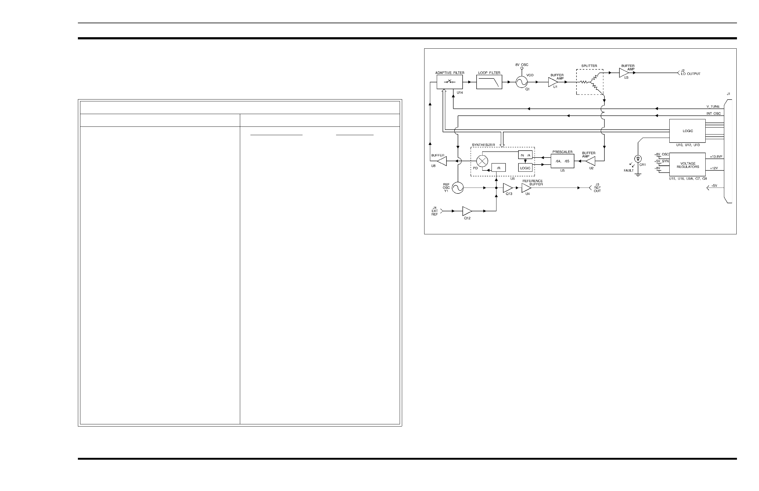
The divided reference signal and the divided VCO signal
are compared in the PLL phase detector. When the reference
and VCO signals are identical the PLL phase detector generates
a constant DC output voltage. This voltage is buffered by U8
and filtered by the loop filter circuit. It is then applied to Q1
setting the VCO on frequency.
If the compared frequencies (phases) differ, an error voltage
is generated which adjusts the VCO frequency. During this
out-of-lock condition, the PLL also sends a Lock Detect signal
(LD) to the controller and lights the FAULT LED on the front
panel of the module.
CIRCUIT ANALYSIS
The Receiver Synthesizer Module consists of the follow-
ing circuits:
•Voltage Controlled Oscillator
•Buffer Amplifiers
•Reference Oscillator and Buffer
•Prescaler and Synthesizer
•Loop Filter
•Digital Control
•Voltage Regulators
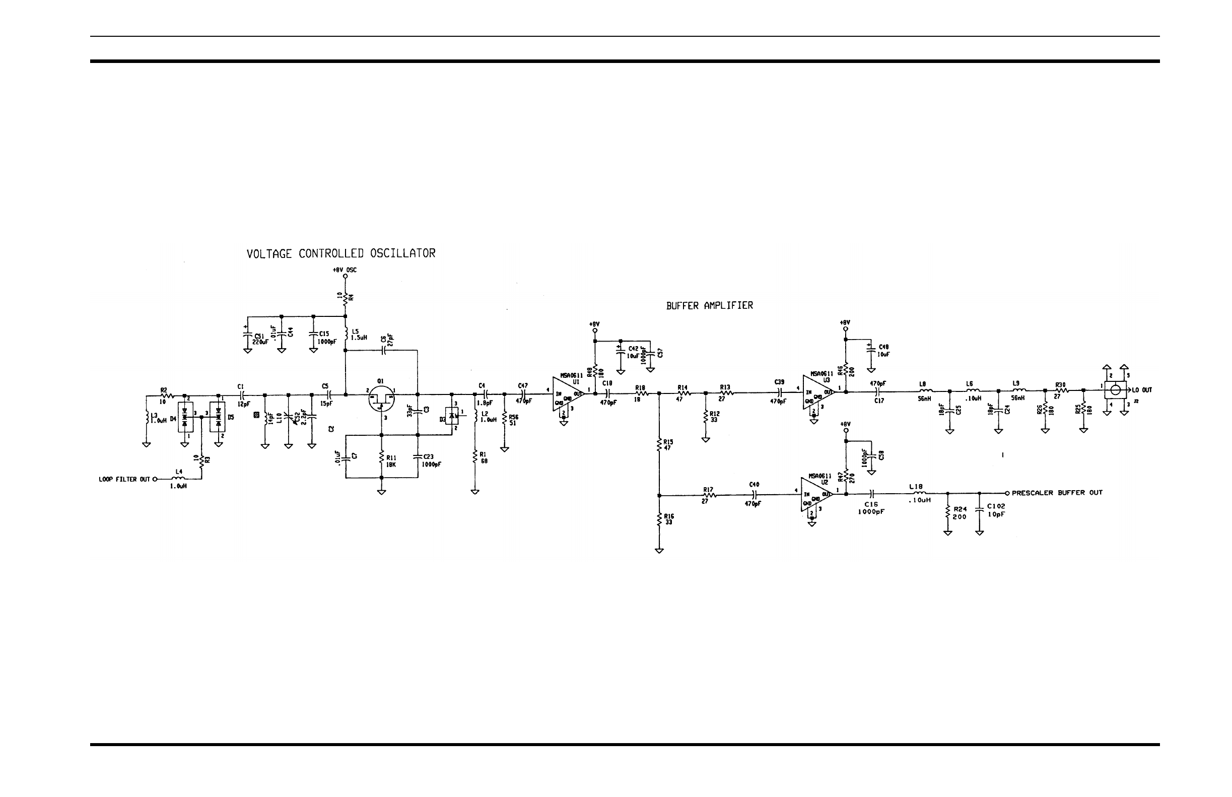
VOLTAGE CONTROLLED OSCILLATOR
The free running Voltage Controlled Oscillator (VCO) is
composed of a grounded-gate JFET (Q1) and associated
circuitry. Inductor L10 and associated capacitors form the
resonant tank circuit. The circuit’s use of high-Q components
minimizes phase noise.
Frequency tuning of the VCO is done by changing the
DC output voltage level from the loop filter U14. The Loop
Filter Out signal from U14 is routed through L4 and R3 and
applied to the two varicap diodes D4 and D5. The voltage
level applied determines the diodes’ capacitance and sets the
resonant frequency of the oscillator. If the VCO drifts or the
frequency is changed, the DC voltage level changes causing
the VCO’s resonant frequency to change. The output of the
oscillator is then applied to a buffer amplifier. Course adjust-
ment of frequency is done by adjusting trimmer capacitor
C52 while applying a calibration voltage to the V_TUNE
line connected to U14.4-11.
BUFFER AMPLIFIERS
The MMIC Buffer Amplifier stage is composed of three
MMICs (U1, U2, and U3) and a resistive splitter. The ampli-
fiers serve two purposes; amplifying the local oscillator
signal (LO OUTPUT) for injection into the Receiver Front
End assembly and providing a feedback signal to the synthe-
sizer Phase-Locked Loop (PLL).
Copyright© 1992-2002, M/A-COM Private Radio Systems, Inc. All rights reserved.
TABLE 1 - GENERAL SPECIFICATIONS
ITEM SPECIFICATION
FREQUENCY TUNING
Output Injection Signal INJECTION FREQ. FREQ. BAND
157.4 MHz - 172.2 MHz (G1) 136 MHz - 150.8 MHz
129.4 MHz - 152.6 MHz (G2) 150.8 MHz - 174 MHz
Electrical
Full Specifications
Degraded Specifications
Channel Spacing
2 MHz
3 MHz
5 kHz
FREQUENCY STABILITY ±1.5 ppm
LO POWER OUTPUT 1.5 dBm ±1.5 dBm
LO NOMINAL IMPEDANCE 50 Ohms
PHASE NOISE
@ 25 kHz Offset
@ 30 kHz Offset -142 dBc/Hz
-147 dBc/Hz
HUM AND NOISE
Companion Receiver -60 dB
HARMONICS @ LO PORT <-30 dBc
SWITCHING SPEED < 50 ms
CURRENT DRAIN
+13.8V
+12V
<200 mA
<50 mA
REFERENCE OSCILLATOR
Frequency Output
Power Output
Impedance
12.8 MHz ±1.5 ppm
0 dBm ±1.5 dBm
50 ohms
EXT. REFERENCE OSCILLATOR
Frequency Output
Power Output
Impedance
5.00 MHz to 17.925 MHz (must be divisible by the
channel spacing)
10 dBm ±3 dBm into 50 ohms
50 ohms
Figure 1 - Receiver Synthesizer Block Diagram
LBI-38641F
1

Integrated circuits U1 and U3 provide amplification of
the local oscillator signal. The output of U1 is fed to a
resistive signal splitter composed of R13 through R18. One
of the resistive signal splitter outputs drives amplifier U3.
The U3 output signal is coupled by C17 to a low-pass filter
network (C24 and C25, L6, L8, and L9) and a resistive pad
(R25, R26 and R30) for isolation. The local oscillator signal
is finally routed to J2, LO OUT, for connection to the
Receiver Front End Assembly. The LO output level at BNC
connector J2 is nominally 0 dBm.
The other output of the resistive signal splitter drives U2.
The amplified output from U2, PRESCALER BUFFER
OUT, is coupled to the 50 ohm input of the prescaler U5 via
capacitors C16 and C45.
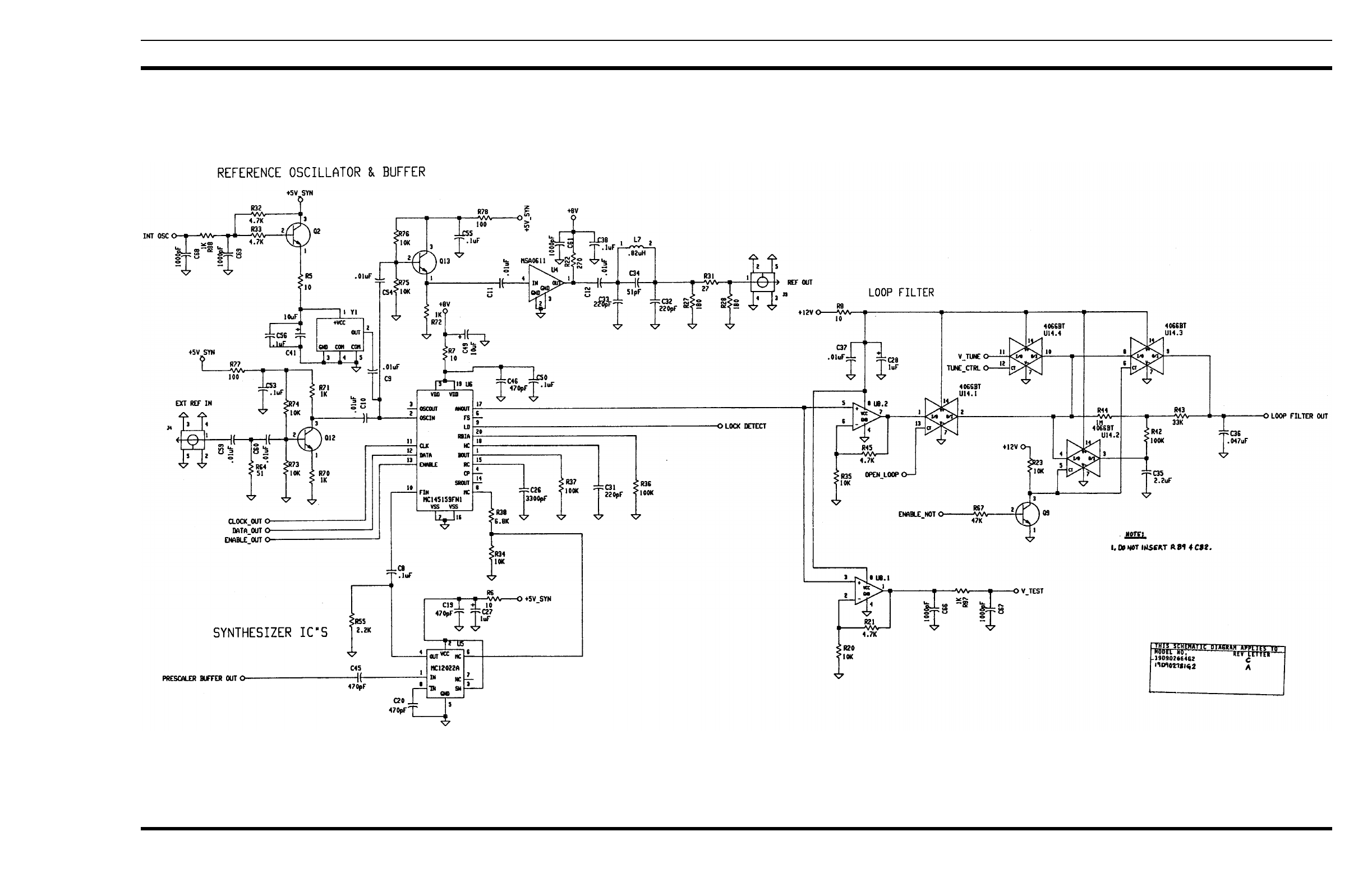
REFERENCE OSCILLATOR AND BUFFER
The reference oscillator section provides a reference
signal to the PLL section. The circuit design allows using
either an external or internal oscillator.
When using an external oscillator, the internal oscillator
is disabled by placing a logic low on the INT OSC line from
the T/R Shelf Interface Board. A high precision external
oscillator may then be connected to the module through the
external reference oscillator connector J4, EXT REF IN. J4
has a 50 ohm input impedance and is coupled to the base of
Q12. Buffer Q12 conditions the signal and applies it to the
synthesizer U6 via coupling capacitor C10.
The internal reference oscillator, Y1, provides a 12.8
MHz signal with a stability of ±1.5 ppm. It is enabled by
applying a logic high signal on the INT OSC line. This signal
turns on Q2, allowing it to conduct and apply +5 volts to pin
1 of the oscillator Y1. The 12.8 MHz output signal (Y1 pin
2) is then sent to the synthesizer via coupling capacitor C9.
The reference oscillator signal, either external or inter-
nal, is also routed to Q13 via coupling capacitor C54. The
output taken from the emitter of Q13 is applied through C11
to the input of Buffer Amplifier U4. The buffered signal is
coupled through C12 to a low pass filter network
(C32,C33,C34, and L7) and a resistive pad (R27, R28, and
R31) for isolation. The output from the resistive pad is then
connected to J3, REF OUT, making the reference oscillator
signal available for external use.
PRESCALER AND SYNTHESIZER IC
The integrated circuit U6 is the heart of the synthesizer.
It contains the necessary frequency dividers and control
circuitry to synthesize output frequencies by the technique
of dual modulus prescaling. U6 also contains an analog
sample and hold phase detector and a lock detector circuit.
Within the U6 are three programmable dividers which
are serially loaded using the CLOCK, DATA, and ENABLE
inputs (pins 11, 12, and 13 respectively). A serial data stream
(DATA) on pin 12 is shifted into the internal shift registers
by low to high transitions on the clock input (CLOCK) at pin
11. A logic high (ENABLE) on pin 13 then transfers the
program information from the shift registers to the divider
latches. The serial data determines the VCO frequency by
setting the internal R, A, and N dividers.
The 12.8 MHz reference oscillator signal OSCIN is in-
ternally routed to the "R" divider. The "R" divider divides
down the 12.8 MHz reference signal to a lower frequency,
Fr, as directed by the input data and applies the signal to the
internal analog phase and lock detectors.
The "A" and "N" dividers process the loop feedback
signal from the VCO (by way of the dual modulus prescaler
U5). The output of the "N" divider, Fv, is a divided down
version of the VCO output frequency. This signal is also
applied to the internal phase detector. The ramp and hold
constants are determined by C26, R37, C31, and R36.
The analog phase detector output voltage (PD OUT) is
proportional to the phase difference between Fv and Fr. This
output serves as the loop error signal. When operating on the
correct frequency, the inputs to the phase detector are iden-
tical and the output voltage of the analog phase detector is
constant. If the compared frequencies (phases) differ, the
analog phase detector increases or decreases the DC output
voltage (PD OUT). This error signal voltage tunes the VCO
to whatever frequency is required to keep Fv and Fr locked
(in phase).
The lock detector furnishes the Fault circuit in U13 with
the lock detect (LD) signal. When Fv and Fr are in phase, the
lock detector output sends a logic high on the LD line to the
fault circuit U13. If the VCO is not locked onto the correct
frequency, the resulting out-of-phase condition causes the
output from the lock detector to be a logic low.
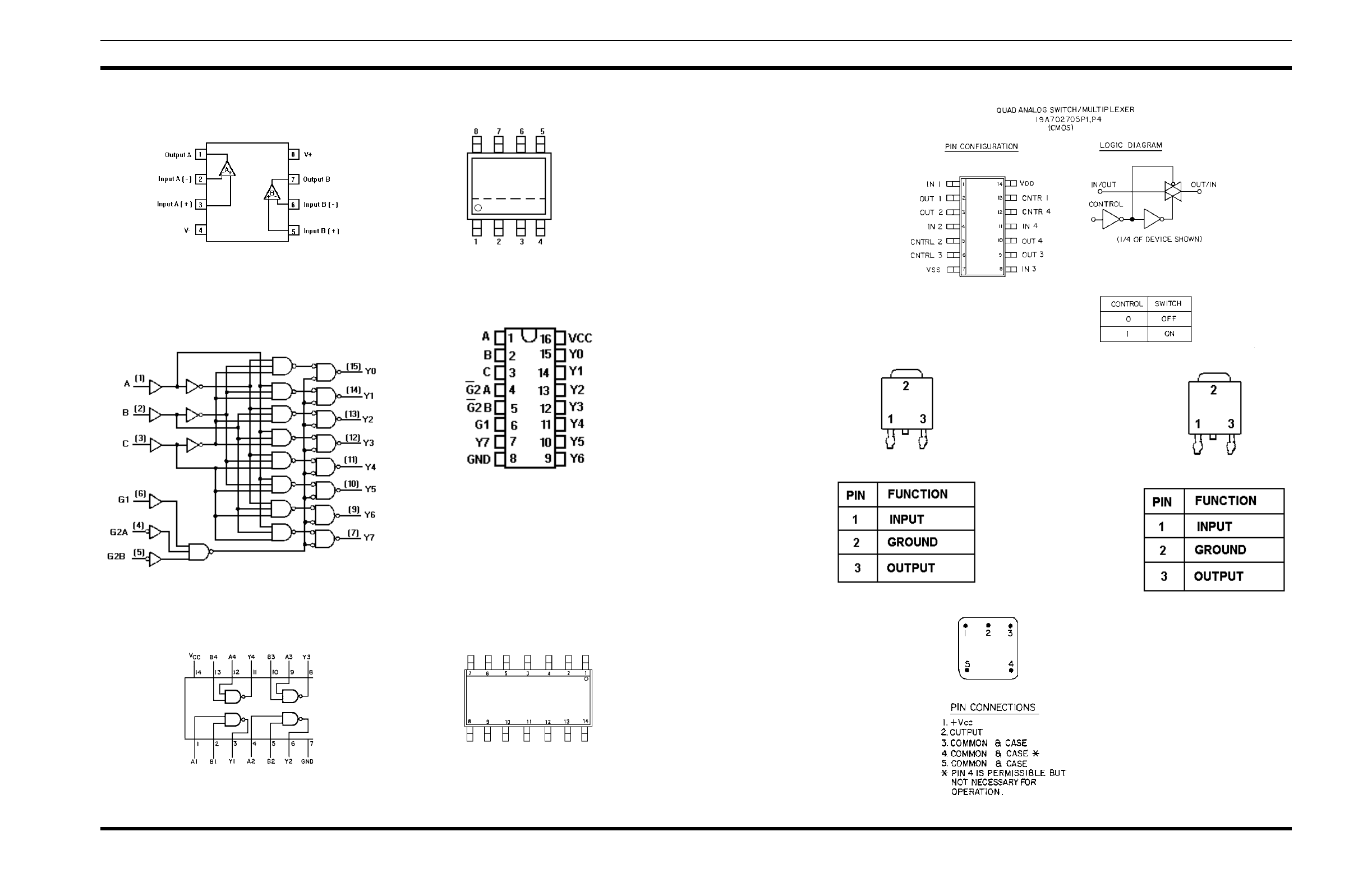
LOOP FILTER
The error signal, ANOUT, is applied to the loop filter at
U8.2-5 and U8.1-3. U8.2 acts as a buffer amplifier with gain.
The output signal from the amplifier is applied to a loop filter
consisting of R42, R43, R44, C35 and C36 via the bilateral
switch U14. The filter removes noise and sampling frequen-
cies from the error voltage. The switch, U14, selects the
proper filter configuration for operation in the narrow band,
wide band or tuning mode. The control signals
(OPEN_LOOP, ENABLE_NOT, and TUNE_CTRL) for
U14 are derived from the digital control circuits U10, U12, and
U13. U8.1 provides a buffered output for testing at the DIN
connector on the rear of the module.
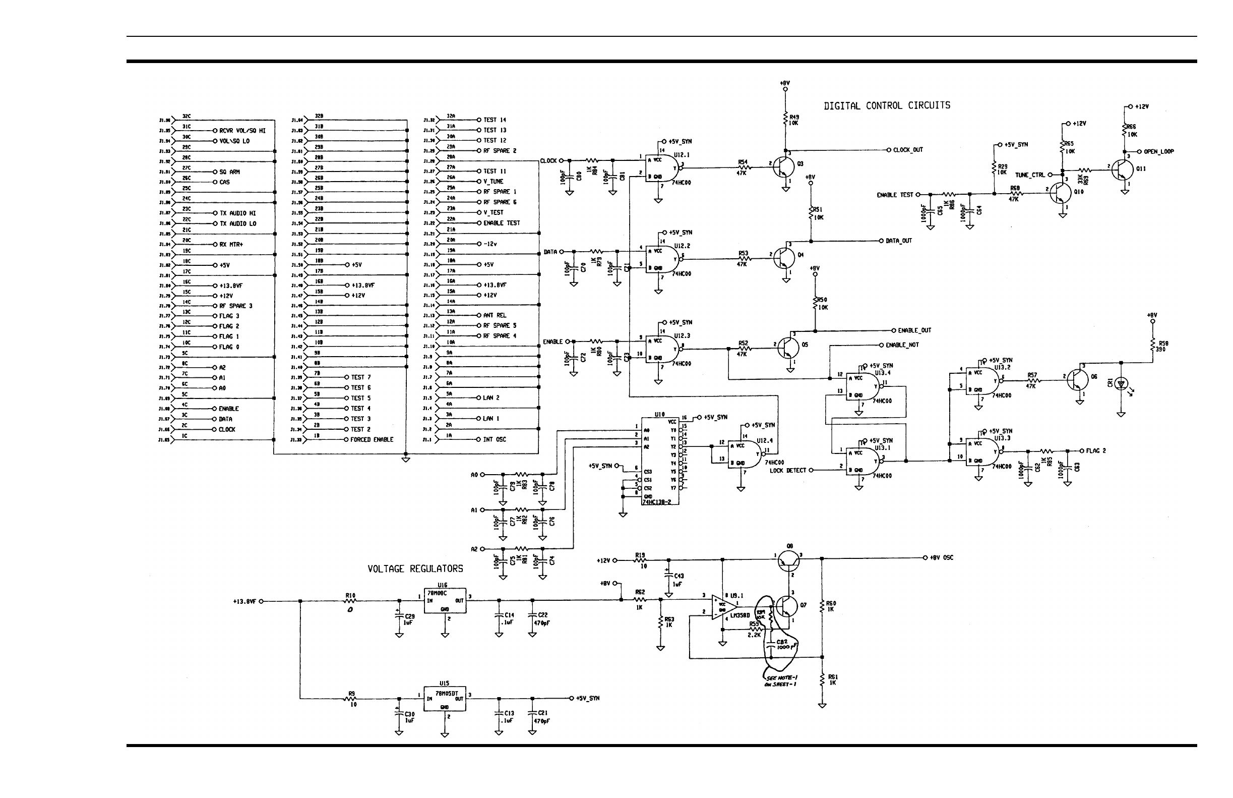
DIGITAL CONTROL
Logic control circuits (other than those inside the synthe-
sizer IC - U6) consist of the following:
•Digital Control Circuit (U10, U12, & U13)
•Level Shifters
•Fault Circuit
The Digital Control Circuits U10, U12, & U13 serve as an
interface between the controller and the synthesizer IC.
As an address decoder, U10 enables the input gates when
the A0, A1, and A2 input lines (pins 4, 3, and 2) receive the
correct address code from the controller. For the Receiver
synthesizer the enable address is 010 on A0, A1, and A2
respectively. After receiving the proper logic code, the input
gate U12 is enabled. This allows the ENABLE, CLOCK, and
serial DATA information to pass on to the synthesizer via the
level shifters.
The Level Shifters Q3, Q4, and Q5 convert the five (5) volt
logic level to the eight (8) volt logic level required by the
synthesizer.
The Fault circuit, U13, monitors the lock detect signal from
the PLL synthesizer. Under normal (locked) condition, the PLL
sends a logic high signal to U13. U13 processes the signal and
providing a logic high output which saturates Q6. With Q6
saturated, the FAULT LED (CR1) turns off. U13 also sends a
logic high signal, FLAG 2, (U13.3-8) to the controller indicat-
ing the VCO’s frequency is correct.
When the VCO is not on the correct frequency, the synthe-
sizer sends a logic low signal to U13. This causes U13 to cutoff
Q6 which turns on the FAULT LED. U13 also sends a logic
low signal to the controller indicating the VCO’s frequency is
incorrect.
VOLTAGE REGULATORS
Voltage regulators U15 and U16 reduce the +13.8 VF line
to +5 Vdc and +8 Vdc respectively. The output from U15
(+5V_SYN) is used by both the synthesizer and logic circuitry
while the 8 Vdc output from U16 is used for the op-amps, level
shifters, and the discrete +8V OSC regulator circuit.
The discrete +8V OSC regulator circuit is a linear regulator
consisting of U9A, Q7, Q8, and associated circuitry. The error
amplifier U9A controls Q7 and pass element Q8. The +8V OSC
is used as the power source for the VCO circuit, where addi-
tional filtering is provided to keep noise to a minimum
MAINTENANCE
RECOMMENDED TEST EQUIPMENT
The following test equipment is required to test the Synthe-
sizer Module:
1. Modulation Analyzer; HP 8901A, or equivalent
2. Power Supply; 12.0 Vdc @ 500 mA
3. Frequency Counter; 10 MHz - 250 MHz
4. Power Meter; -20 dBm to +10 dBm
5. Spectrum Analyzer; 0 - 1 GHz
TEST AND ALIGNMENT
Initialization
Apply +12 Vdc to the test fixture.
Current consumption
Measure the current through pins 15A,15B, 15C, 16A, 16B,
and 16C.
Verify the current is less than 250 mA. Total current
is the +13.8 VF current and +12 Vdc current com-
bined.
Reference Oscillator
Adjust Y1 for an output frequency of 12.8 MHz ±5 Hz.
Measure the output power of the reference oscillator output
(J3).
Verify the output power is 0 dBm ±1.5 dBm.
Oscillator Alignment
Ground the ENABLE TEST line (pin 22A). Apply +5 Vdc
to the V_TUNE line (pin 26A). Measure the frequency of the
free running oscillator at the LO OUT port (J2).
LBI-38641F
2
Adjust the trimmer capacitor C52 to the correct frequency:
Group 1 - 170 MHz ±100 kHz.
Group 2 - 150 MHz ±100 kHz.
Synthesizer Loading
Unground the ENABLE TEST line (pin 22A). Load the
synthesizer IC Group 1 - 170 MHz.
Group 2 - 150 MHz.
Verify the lock indicator (CR1) is off or the FLAG 2 line is
high.
Hum and Noise
Initialize the HP 8901A for 300 Hz - 3 kHz, 750 us deem-
phasis, average FM deviation, and 0.44 dB reference for the
deviation.
Verify the hum and noise (J2) is less than -55 dB.
Output Power and Harmonic Content
Verify the output power (J2) at the fundamental frequency
is:
0 dBm ±2.0 dB
Verify the harmonic content is less than -30dBc.
Continued
The following service information applies when
aligning, testing, or troubleshooting the RX Synthe-
sizer:
•Logic Levels:
Logic 1 = high = 4.5 to 5.5 Vdc
Logic 0 = Low = 0 to 0.5 Vdc
•Receiver Synthesizer Address = A0 A1 A2 = 010
•Synthesizer data input stream is as follows:
14-bit "R" divider most significant bit (MSB)
= R13 through "R" divider least significant bit
(LSB) = R0
10-bit "N" divider MSB = N9 through "N"
divider LSB = N0
7-bit "A" divider MSB = A6 through "A" divider
LSB = A0
Single high Control bit (last bit)
Latched When Control Bit = 1
DATA ENTRY FORMAT
Latched When
Control Bit = 1
•Synthesizer lock is indicated by the extinguishing
of the front panel LED indicator and a logic high
on the fault FLAG 2 line (J1 pin 12C).
•Always verify synthesizer lock after each new data
loading.
Shift
→Register
Out
Control Bit
SERVICE NOTES
Data→Last
bit A0
LSB - - - A6
MSB N0
LSB - - - N9
MSB R0
LSB - - - R13
MSB
TROUBLESHOOTING CHART
SYMPTOM AREAS TO CHECK INDICATIONS
I. Loop Fails To Lock 1. Check for:
+8 Vdc at U16-3,
+5 Vdc at U15-3
+8 Vdc at Q8-C.
Bad Regulation circuitry.
Troubleshoot using standard
procedures.
2. Check for 12.8 MHz reference
at U6-2, and U6-3.
Typical Levels:
500 mVpp @ U6-2
2.5 Vpp @ U6-3
Reference Osc. Module defective or
supply not present or low. Proceed to
reference oscillator section II.
3. Check for LO output @ J2.
FLO ±5 MHz,0dBm nominal.
LO tuning incorrect, or buffer
amplifier bad. Proceed to LO tuning
and power section III.
4. Check Prescaler output @
U5-4.
Typically: 2-4 MHz square
wave @ 1.25 Vpp.
If LO power is good, Check for 3.2
Vdc @ U2-3. Replace U2, then U5 if
necessary.
5. Check for CLOCK, DATA, and
ENABLE signals are reaching
U6 pins 11,12, and 13 respec-
tively. (0, 8V logic levels)
Bad digital control circuitry.
Troubleshoot using standard
procedures. Ensure all programming
signals are present at J1.
(CLOCK,DATA,ENABLE,A0,A1
and A2)
6. Check Ramp Signal @ U6-15.
It should be 5 kHz nominal. If reference oscillator and
programming signals are present for
proper programming information.
Last resort - replace Synthesizer IC
U6.
II. Reference OSC. not present or
low power. 1. Check for 4.3 Vdc supply at
junction of R5 and C41. Bad supply switch Q2 or wrong
Control Signal Internal Osc.
Troubleshoot using standard
procedures. Replace Y1 as last resort
2. Check 12.8 MHz signal @
Q13-E. Should be approx. 350
mVpp.
Bad buffer amplifier Q13.
Troubleshoot using standard
procedures.
LBI-38641F
3
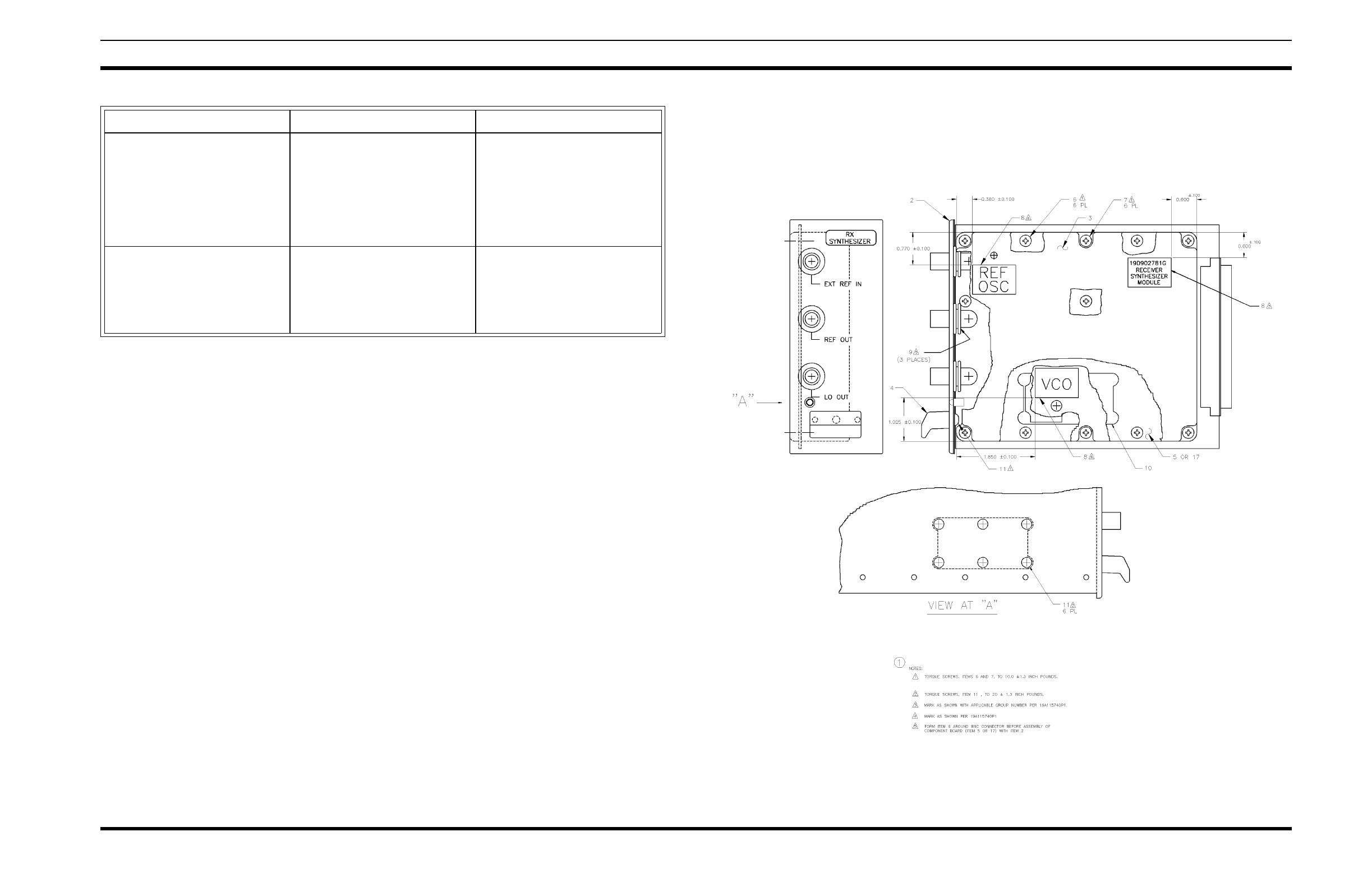
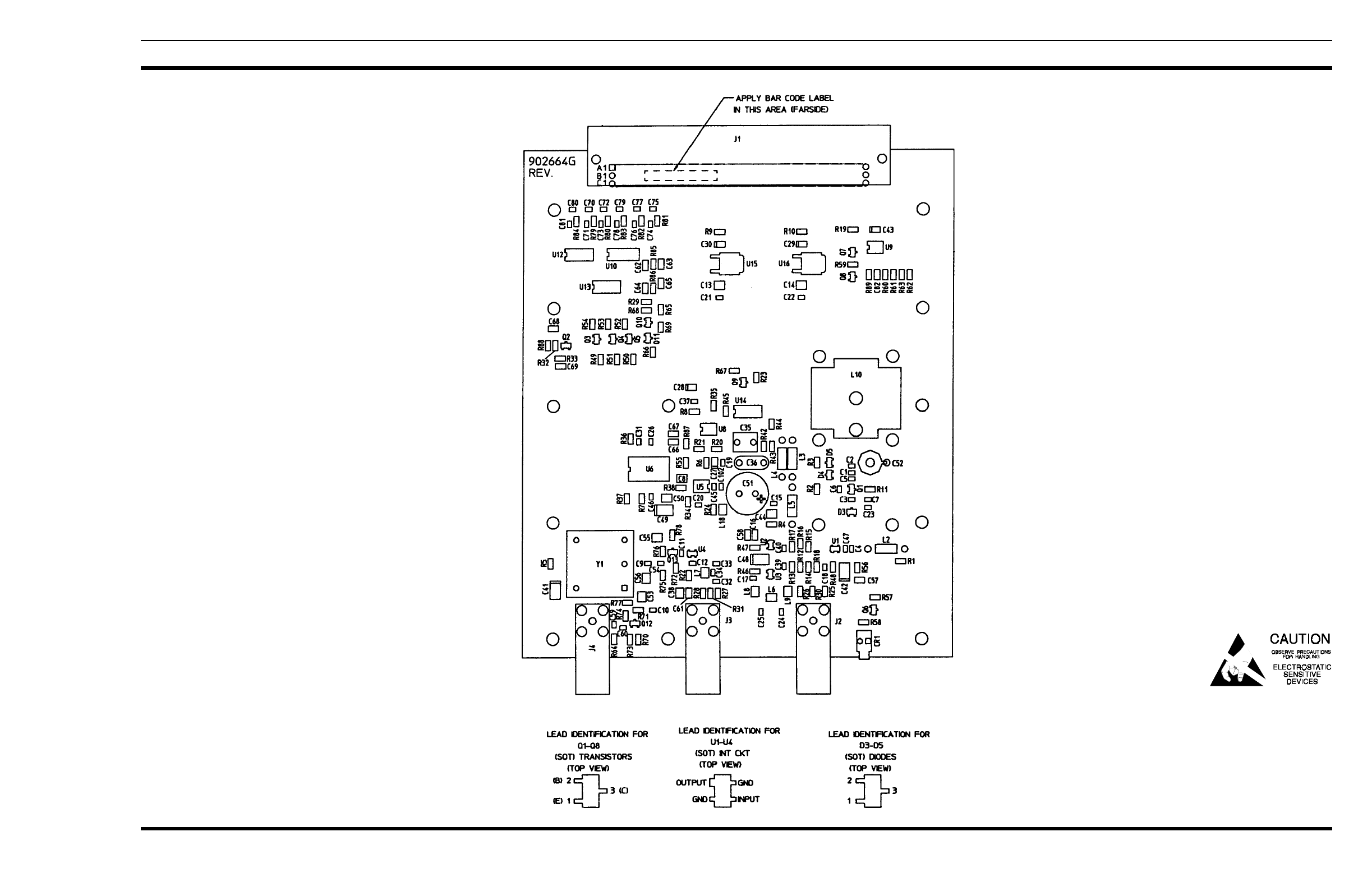
ASSEMBLY DIAGRAM
RECEIVER SYNTHESIZER MODULE
19D902781G1 & G2
(19D902781, Sh1, Rev. 7)
TROUBLESHOOTING CHART (Continued)
SYMPTOM AREAS TO CHECK INDICATIONS
III. LO power low or tuned out of
band. 1. Check tuning with 6 Vdc
applied using test procedure.
FLO±5 MHz
LO tuning incorrect. Retune
following test procedure.
2. Check DC bias at Buffer
Amplifiers U1, U2, & U3 pin 3
Typ. 3.2 Vdc.
Bad Buffer Amplifier. Replace bad
part.
IV. LO signal not present. (i.e. Q1
does not oscillate) 1. Check DC bias at Q1 drain.
(Typ. +8Vdc) Replace Q1.
2. Check DC bias at Q1 source.
(Typ. +0.9 Vdc)
LBI-38641F
4
OUTLINE DIAGRAM
RECEIVER SYNTHESIZER BOARD
19D902664G1 & G2
(19D902664, Sh. 1, Rev. 10)
LBI-38641F
5
SCHEMATIC DIAGRAM
RECEIVER SYNTHESIZER BOARD
19D902664G1
(19D903621, Sh. 1, Rev. 4)
LBI-38641F
6
SCHEMATIC DIAGRAM
RECEIVER SYNTHESIZER BOARD
19D902664G1
(19D903621, Sh. 2, Rev. 4)
LBI-38641F
7
SCHEMATIC DIAGRAM
RECEIVER SYNTHESIZER BOARD
19D902664G1
(19D903621, Sh. 3, Rev. 4)
LBI-38641F
8
SCHEMATIC DIAGRAM
RECEIVER SYNTHESIZER BOARD
19D902664G2
(19D903769, Sh. 1, Rev. 3)
LBI-38641F
9
SCHEMATIC DIAGRAM
RECEIVER SYNTHESIZER BOARD
19D902664G2
(19D903769, Sh. 2, Rev. 3)
LBI-38641F
10
SCHEMATIC DIAGRAM
RECEIVER SYNTHESIZER BOARD
19D902664G2
(19D903769, Sh. 3, Rev. 3)
LBI-38641F
11
PARTS LIST
SYMBOL PART N0. DESCRIPTION
— — — MISCELLANEOUS — —
2 19D902508P3 Chassis.
3 19D902509P3 Cover.
4 19D902555P1 Handle.
5 19D902664G1 Receiver Synthesizer Board, (Used in
G1).
6 19A702381P506 Screw, thread forming: TORX, No.
M3.5 - 0.6 X 6.
7 19A702381P513 Screw, thread forming: TORX, No.
M3.5 - 0.6 X 13.
9 19B802690P1 RF Shielding Grommet.
10 19D902824P1 RF Casting.
11 19A702381P508 Screw, thd. form: No. 3.5-0.6 x 8.
(Used in G1, G2, G1 and G2).
17 19D902664G2 Receiver Synthesizer Board.
(Used in G2).
RECEIVER SYNTHESIZER BOARD
19D902664G1 - G2
— — — — CAPACITORS — — —
C1 19A702236P28 Ceramic: 12 pF ±5%, 50 VDCW, temp
coef 0±30 PPM. (Used in G2).
C1 19A702236P23 Ceramic: 8.2 pF ±.25 pF, 50 VDCW,
temp coef 0 ±30 PPM. (Used in G1).
C2 19A702236P10 Ceramic: 2.2 pF ±2.5 pF, 50 VDCW,
temp coef 0 ±30 PPM/°C. (Used in G2).
C2 19A702236P8 Ceramic: 1.5 pF ±.25 pF, 50 VDCW.
(Used in G1).
C3 19A702236P38 Ceramic: 33 pF ±5%, 50 VDCW, temp
coef 0 ±30 PPM/°C. (Used in G2).
C3 19A702236P36 Ceramic: 27 pF ±5%, 50 VDCW, temp
coef 0 ±30 PPM/°C. (Used in G1).
C4 19A702236P9 Ceramic: 1.8 pF ±0.25 pF, 50 VDCW,
temp coef 0 ±30 PPM.
C5 19A702236P30 Ceramic: 15 pF ±5%, 50 VDCW, temp
coef 0 ±30 PPM/°C. (Used in G2).
C5 19A702236P28 Ceramic: 12 pF ±5%, 50 VDCW, temp
coef 0 ±30 PPM. (Used in G1).
C6 19A702236P36 Ceramic: 27 pF ±5%, 50 VDCW, temp
coef 0 ±30 PPM/°C. (Used in G2).
C6 19A702236P34 Ceramic: 22 pF ±5%, 50 VDCW, temp
coef 0 ±30 PPM. (Used in G1).
C7 19A702052P14 Ceramic: 0.01 µF ±10%, 50 VDCW.
C8 19A702052P26 Ceramic: 0.1 µF ±10%, 50 VDCW.
C9 19A702052P14 Ceramic: 0.01 µF ±10%, 50 VDCW.
thru
C12
C13 19A702052P26 Ceramic: 0.1 µF ±10%, 50 VDCW.
and
C14
C15 19A702052P5 Ceramic: 1000 pF ±10%, 50 VDCW.
C16 19A702061P99 Ceramic: 1000 pF ±5%, 50 VDCW,
thru temp coef. 0 ±30 PPM/ºC.
C22
C23 19A702052P5 Ceramic: 1000 pF ±10%, 50 VDCW.
SYMBOL PART NO. DESCRIPTION
C24
and 19A702236P32 Ceramic: 18 pF ±5%, 50 VDCW, temp
C25 coef 0 ±30 PPM
C26 19A702052P8 Ceramic: 3300 pF ±10%, 50 VDCW.
C27 19A705205P2 Tantalum: 1 µF, 16 VDCW;
thru sim to Sprague 293D.
C30
C31 19A702052P1 Ceramic: 220 pF ±10%, 50 VDCW.
thru
C33
C34 19A702236P43 Ceramic: 51 pF ±5, 50 VDCW,
±30 PPM/°C.
C35 19A703684P3 Metallized polyester: 2.2 µF ±10%,
50 VDCW.
C36 19A703902P3 Metal: 0.047 µF ±10%, 50 VDCW.
C37 19A702052P14 Ceramic: 0.01 µF ±10%, 50 VDCW.
C38 19A702052P26 Ceramic: 0.1 µF ±10%, 50 VDCW.
C39 19A702052P3 Ceramic: 470 pF ±10%, 50 VDCW.
and
C40
C41 19A705205P6 Tantalum: 10 µF, 16 VDCW; sim to
and Sprague 293D.
C42
C43 19A705205P2 Tantalum: 1 µF, 16 VDCW; sim to
Sprague 293D.
C44 19A702052P26 Ceramic: 0.1 µF ±10%, 50 VDCW.
C45 19A702052P3 Ceramic: 470 pF ±10%, 50 VDCW.
thru
C47
C48 19A705205P6 Tantalum: 10 µF, 16 VDCW; sim to
and Sprague 293D.
C49
C50 19A702052P26 Ceramic: 0.1 µF ±10%, 50 VDCW.
C51 19A701225P3 Electrolytic: 220 µF, -10+50%,
25 VDCW.
C52 19A134227P5 Variable: 1.5 to 14 pF, 100 VDCW.
C53 19A702052P26 Ceramic: 0.1 µF ±10%, 50 VDCW.
C54 19A702052P14 Ceramic: 0.01 µF ±10%, 50 VDCW.
C55 19A702052P26 Ceramic: 0.1 µF ±10%, 50 VDCW.
and
C56
C57 19A702061P99 Ceramic: 1000 pF ±5%, 50 VDCW,
and temp coef 0 ±30 PPM/°C.
C58
C59 19A702052P14 Ceramic: 0.01 µF ±10%, 50 VDCW.
and
C60
C61 19A702061P99 Ceramic: 1000 pF ±5%, 50 VDCW,
thru temp coef 0 ±30 PPM/°C.
C69
C70 19A702061P61 Ceramic: 100 pF ±5%, 50 VDCW,
thru temp coef 0 ±30 PPM.
C81
C102 19A702236P25 Ceramic: 10 pF ±25pF, 50 VDCW,
temp coef. 0 ±30 PPM/ºC.
— — — — DIODES — — — — —
CR1 19A703595P10 Diode, Optoelectric: Red; sim to HP
HLMP-1301-010.
D3 19A705377P1 Silicon, Hot Carrier: sim to MMB0201.
D4 19A149674P1 Silicon, capacitive: sim to Toko KV1410.
and
D5
RECEIVER SYNTHESIZER MODULE
19D902781G1-G2
ISSUE 4
*COMPONENTS, ADDED, DELETED OR CHANGED BY PRODUCTION CHANGES
SYMBOL PART NO. DESCRIPTION
R25 19B800607P151 Metal film: 150 ohms ±5%, 1/8 w.
(Used in G1).
R26 19B800607P181 Metal film: 180 ohms ±5%, 1/8 w.
(Used in G2).
R26 19B800607P151 Metal film: 150 ohms ±5%, 1/8 w.
(Used in G1).
R27 19B800607P181 Metal film: 180 ohms ±5%, 1/8 w.
and
R28
R29 19B800607P103 Metal film: 10K ohms ±5%, 1/8 w.
R30 19B800607P270 Metal film: 27 ohms ±5%, 1/8 w.
(Used in G2).
R30 19B800607P390 Metal film: 39 ohms ±5%, 1/8 w.
(Used in G1).
R31 19B800607P270 Metal film: 27 ohms ±5%, 1/8 w.
R32 19B800607P472 Metal film: 4.7K ohms ±5%, 1/8 w.
and
R33
R34 19B800607P103 Metal film: 10K ohms ±5%, 1/8 w.
and
R35
R36 19B800607P104 Metal film: 100K ohms ±5%, 1/8 w.
and
R37
R38 19B800607P682 Metal film: 6.8K ohms ±5%, 1/8 w.
R42 19B800607P104 Metal film: 100K ohms ±5%, 1/8 w.
(Used in G2).
R42 19B800607P333 Metal film: 33K ohms ±5%, 1/8 w.
(Used in G1).
R43 19B800607P333 Metal film: 33K ohms ±5%, 1/8 w.
R44 19B800607P105 Metal film: 1M ohms ±5%, 1/8 w.
R45 19B800607P472 Metal film: 4.7K ohms ±5%, 1/8 w.
R46 19B800607P201 Metal film: 200 ohms ±5%, 1/8 w.
(Used in G2).
R46 19B800607P181 Metal film: 180 ohms ±5%, 1/8 w.
(Used in G1).
R47 19B800607P271 Metal film: 270 ohms ±5%, 1/8 w.
R48 19B800607P181 Metal film: 180 ohms ±5%, 1/8 w.
R49 19B800607P103 Metal film: 10K ohms ±5%, 1/8 w.
thru
R51
R52 19B800607P473 Metal film: 47K ohms ±5%, 1/8 w.
thru
R54
R55 19B800607P222 Metal film: 2.2K ohms ±5%, 1/8 w.
R56 19B800607P510 Metal film: 51 ohms ±5%, 1/8 w.
R57 19B800607P473 Metal film: 47K ohms ±5%, 1/8 w.
R58 19B800607P681 Metal film: 680 ohms ±5%, 1/8 w.
R59 19B800607P222 Metal film: 2.2K ohms ±5%, 1/8 w.
R60 19B800607P102 Metal film: 1K ohms ±5%, 1/8 w.
thru
R63
R64 19B800607P510 Metal film: 51 ohms ±5%, 1/8 w.
R65 19B800607P103 Metal film: 10K ohms ±5%, 1/8 w.
and
R66
R67 19B800607P473 Metal film: 47K ohms ±5%, 1/8 w.
and
R68
SYMBOL PART NO. DESCRIPTION
J1 19B801587P7 Connector, DIN: 96 male contacts, right
angle mounting; sim to AMP 650887-1.
J2 19A115938P24 Connector, receptacle.
thru
J4
— — — — INDUCTORS — — —
L2 19A700024P13 Coil, RF: 1.0 µH ±10%.
thru
L4
L5 19A700024P15 Coil, RF: 1.5 µH ±10%.
L6 19A705470P13 Coil: 0.10 µH ±20%. (Used in G2).
L6 19A705470P12 Coil, fixed. (Used in G1).
L7 19A705470P24 Coil, fixed: 1.5 µH ±10%.
L8 19A705470P10 Coil, fixed: 56 nH ±20%. (Used in G2).
L8 19A705470P9 Coil, Fixed: 47 nH; sim to Toko
380NB-47nM. (Used in G1).
L9 19A705470P10 Coil, fixed: 56 nH ±20%. (Used in G2).
L9 19A705470P9 Coil, Fixed: 47 nH; sim to Toko
380NB-47nM. (Used in G1).
L10 19C851001P3 Coil, RF: sim to Paul Smith SK-901-1.
(Used in G2).
L10 19C851001P1 Coil, RF: sim to Paul Smith SK901-1.
(Used in G1).
L18 19A705470P13 Coil: 0.10 µH ±20%
— — — TRANSISTORS — — —
Q1 19A702524P2 N-Type, field effect; sim to
MMBFU310.
Q2 19A700076P2 Silicon, NPN: sim to MMBT3904, low
thru profile.
Q7
Q8 19A700059P2 Silicon, PNP: sim to MMBT3906, low
profile.
Q9 19A700076P2 Silicon, NPN: sim to MMBT3904, low
thru profile.
Q13
— — — — RESISTORS— — — —
R1 19B800607P680 Metal film: 68 ohms ±5%, 1/8 w.
R2 19B800607P100 Metal film: 10 ohms ±5%, 1/8 w.
thru
R9
*R10 19B800607P1 Metal film: 0 ohms.
R11 19B800607P183 Metal film: 18K ohms ±5%, 1/8 w.
R12 19B800607P330 Metal film: 33 ohms ±5%, 1/8 w.
R13 19B800607P270 Metal film: 27 ohms ±5%, 1/8 w.
R14 19B800607P470 Metal film: 47 ohms ±5%, 1/8 w.
and
R15
R16 19B800607P330 Metal film: 33 ohms ±5%, 1/8 w.
R17 19B800607P270 Metal film: 27 ohms ±5%, 1/8 w.
R18 19B800607P180 Metal film: 18 ohms ±5%, 1/8 w.
R19 19B800607P100 Metal film: 10 ohms ±5%, 1/8 w.
R20 19B800607P103 Metal film: 10K ohms ±5%, 1/8 w.
R21 19B800607P472 Metal film: 4.7K ohms ±5%, 1/8 w.
R22 19B800607P271 Metal film: 270 ohms ±5%, 1/8 w.
R23 19B800607P103 Metal film: 10K ohms ±5%, 1/8 w.
R24 19B800607P201 Metal film: 200 ohms ±5%, 1/8 w.
LBI-38641F
12
IC DATA
PARTS LIST & PRODUCTION CHANGES
SYMBOL PART NO. DESCRIPTION
R70 19B800607P102 Metal film: 1K ohms ±5%, 1/8 w.
thru
R72
R73 19B800607P103 Metal film: 10K ohms ±5%, 1/8 w.
thru
R76
R77 19B800607P101 Metal film: 100 ohms ±5%, 1/8 w.
and
R78
R79 19B800607P102 Metal film: 1K ohms ±5%, 1/8 w.
thru
R88
— — INTEGRATED CIRCUITS —
U1 19A705927P1 Silicon, bipolar: sim to Avantek
thru MSA-0611.
U4
U5 19A149944P201 Dual Modulus Prescaler: sim to
MC12022A.
U6 19B800902P5 Synthesizer, custom: CMOS, serial
input.
U8 19A702293P3 Linear: Dual Op Amp; sim to LM358D.
and
U9
U10 19A703471P320 Digital: 3-Line To 8-Line Decoder;
sim to 74HC138.
U12 19A703483P302 Digital: Quad 2-Input NAND Gate;
and sim to 74HC00.
U13
U14 19A702705P4 Digital: Quad Analog Switch/
Multiplexer; sim to 4066BM.
U15 19A704971P8 Voltage Regulator, Positive: sim to
Motorola MC78M05CDT.
U16 19A704971P10 Voltage Regulator, Positive: sim to
Motorola MC78M08CDT.
— — — — CRYSTALS — — —
Y1 19B801351P12 Crystal Oscillator; 14.850 MHz,
temperature compensated.
U1 thru U4
19A705927P1
Silicon Bipolar IC
U5
19A149944P201
Modulus Prescaler
120
3
2
4
5
6
7
8
10 11
12
13
14
15
16
17
18
19
9
U6
19B800902P7
Synthesizer
PRODUCTION CHANGES
Changes in the equipment to improve or to simplify circuits are identified by a
"Revision Letter", which is stamped after the model number of the unit. The revision
stamped on the unit includes all previous revisions. Refer to the Parts List for
descriptions of parts affected by these revisions.
REV. A - RECEIVER SYNTHESIZER BOARD 19D902664G1 & G2
To improve regulator operation at low supply voltage. Changed resistor
R10. Resistor R10 was 10 ohms (19B800607P100).
REV. B - RECEIVER SYNTHESIZER BOARD 19D902664G1 & G2
To accommodate SOG synthesizer IC package U6 (PLCC package
discontinued) and make provision for RC compensation network (R89,
C82) in 10-Volt regulator circuit. Resistor R89 and capacitor C82 are not
installed. Modified printed wire board layout (Printed wire board changed
from 19D902665P1R1 to 19D902665P1R2). Changed U6. Synthesizer
U6 was 19B800902P5.
REV. A - RECEIVER SYNTHESIZER MODULE 19D902781G1 & G2
To install RF shielding grommets. Installed item 9 RF shielding grommets
(19B705470P1) on three BNC connectors of input/output RF ports.
REV. C - RECEIVER SYNTHESIZER BOARD 19D902664G1 & G2
To add filtering in the output circuit of the pre-scaler buffer amplifier.
Changed capacitor C16. Capacitor C16 was 19A702052P3 (470 pF).
Added capacitor C102 and inductor L18. Changed resistor R24. Resistor
R24 was 19B800607P510 (51 Ohms).
LBI-38641F
13
IC DATA
U8 & U9
19A702293P2
Dual Operational Amplifier
U10
19A703471P120
Decoder/Demux
U12 & U13
19A703483P302
Logic Gate/Inverter
U14
19A702705P4
Quad Analog Switch
U16
19A70497P10
+8V Regulator
U15
19A704971P8
+5 Regulator
Y1
19B801351P12
Crystal Oscillator
LBI-38641F
14

This page intentionally left blank
LBI-38641F
15