HARRIS TR-0017-E Sitepro Base Station User Manual RX IF
HARRIS CORPORATION Sitepro Base Station RX IF
UserManual.wiki
>
HARRIS
>
TR-0017-E User Manual
>
RX IF
Contents
1.
Applications Diagrams
2.
Interface Panels
3.
Main Manual
4.
Power Supply
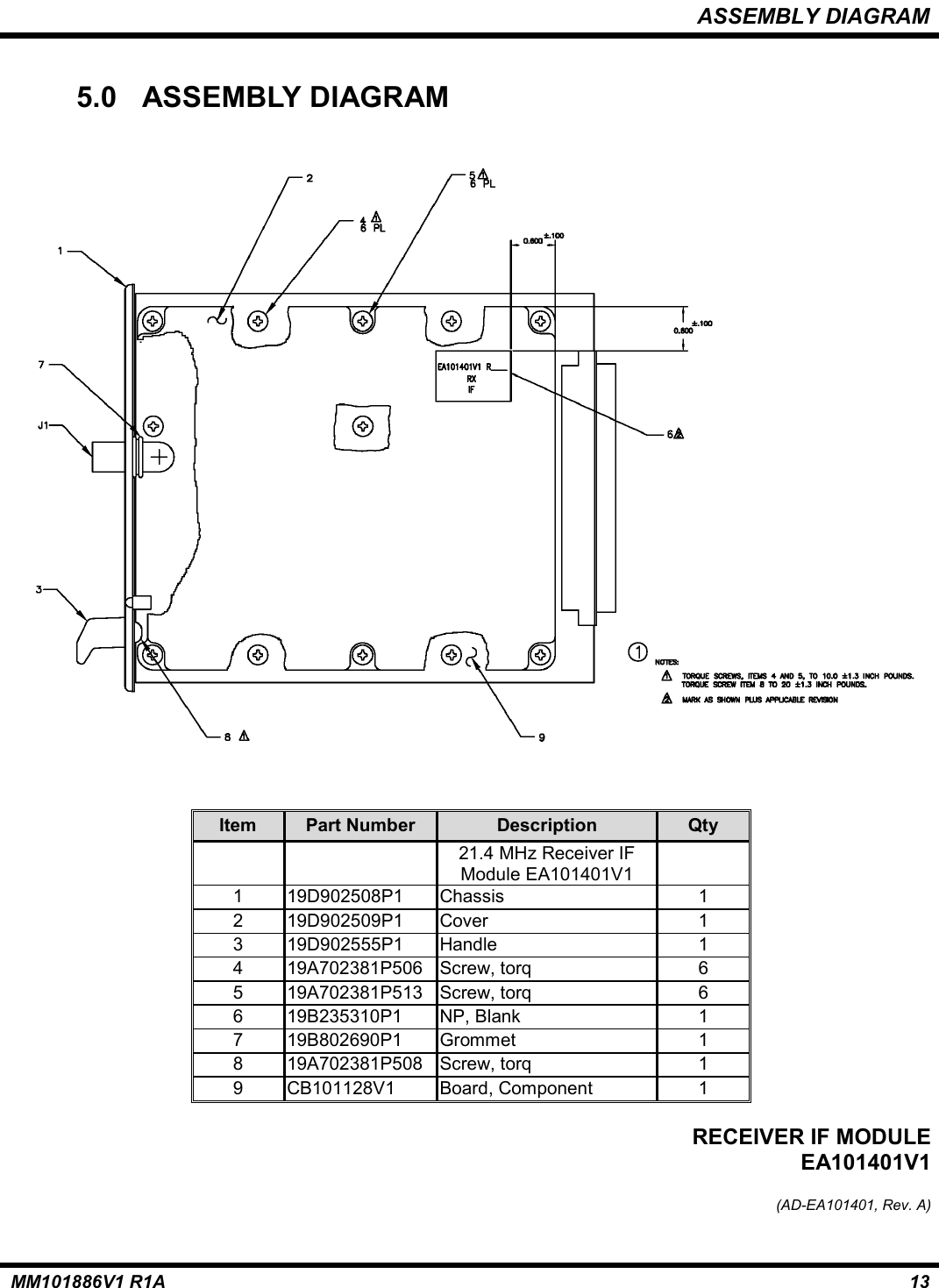
5.
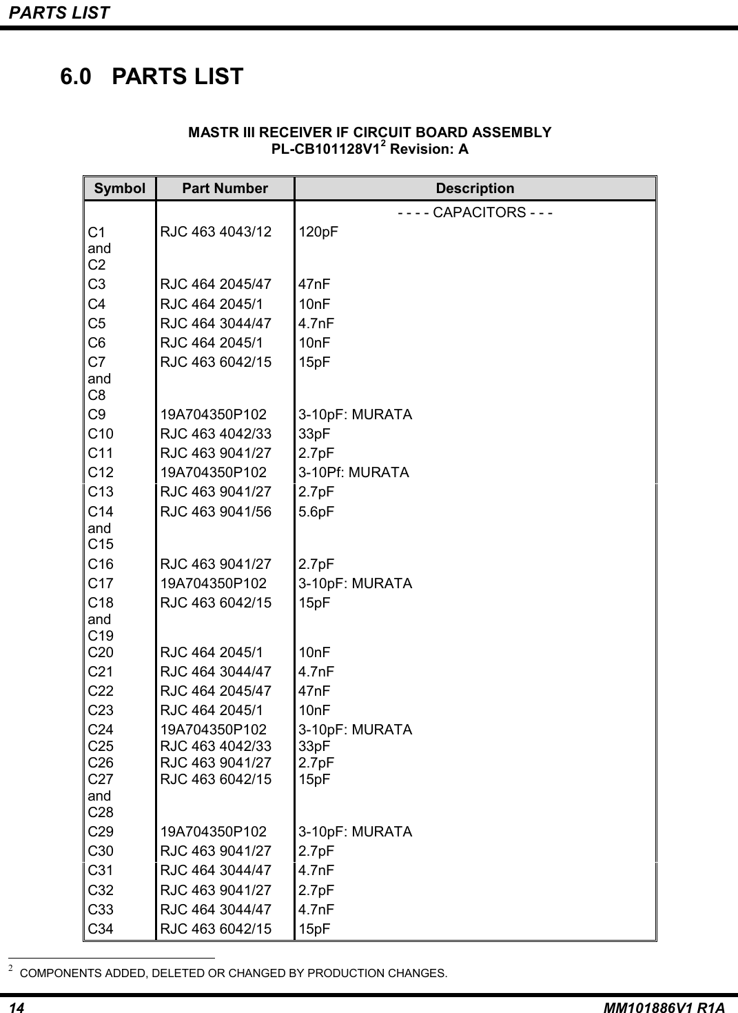
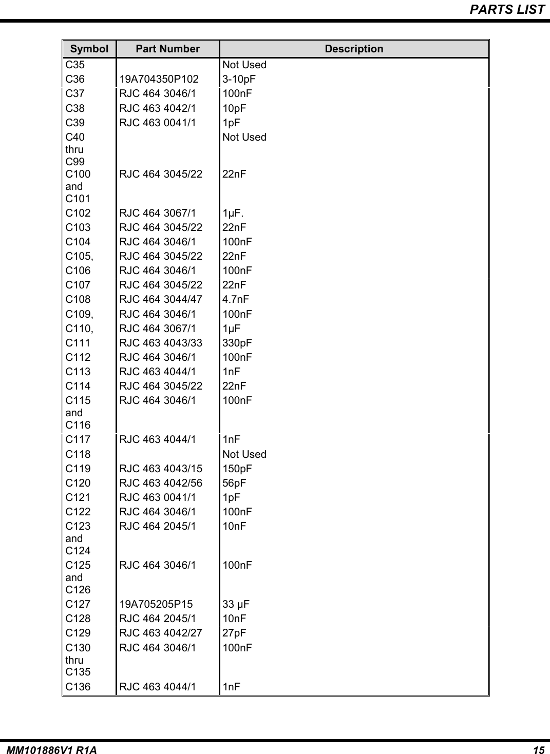
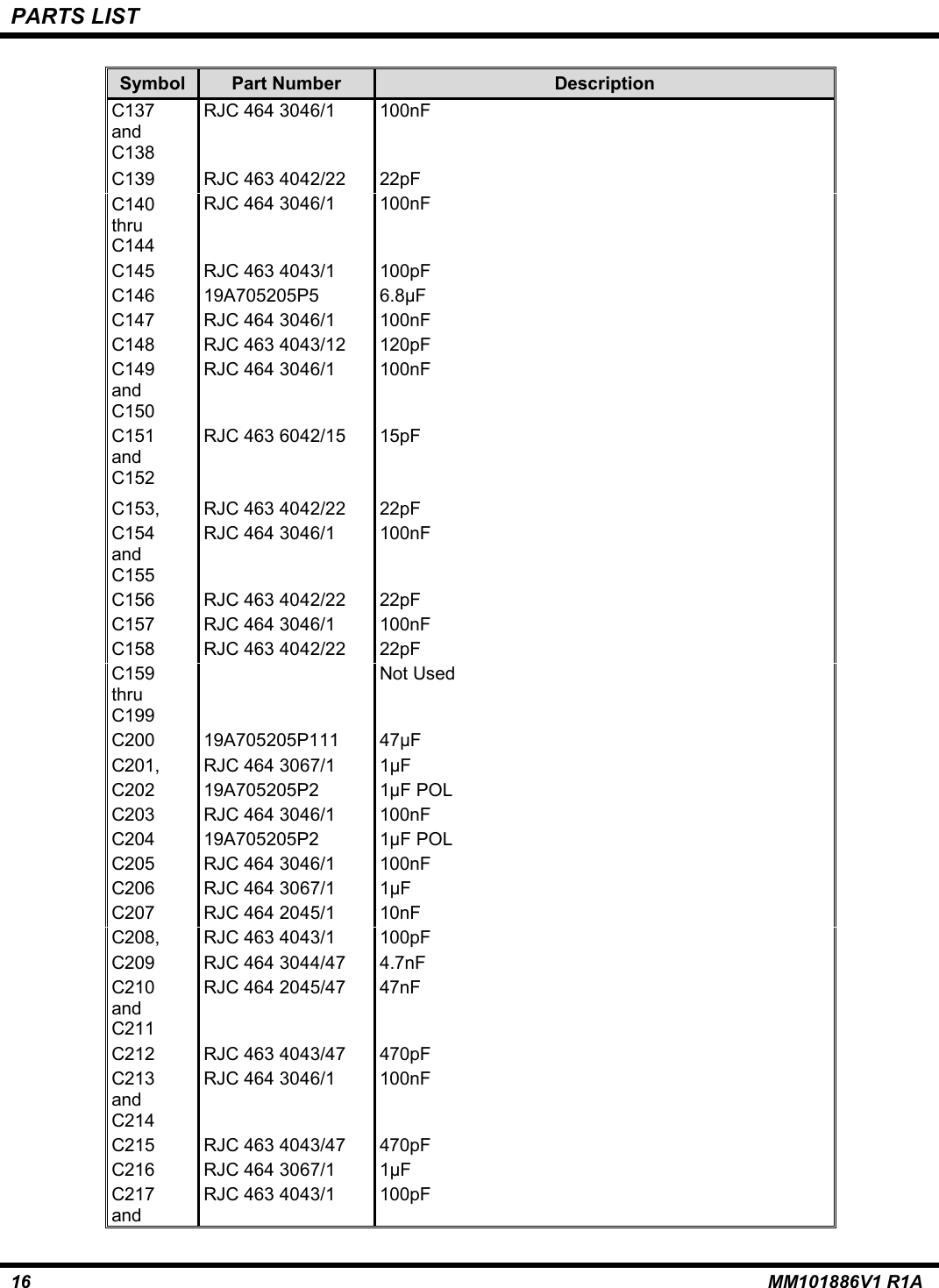
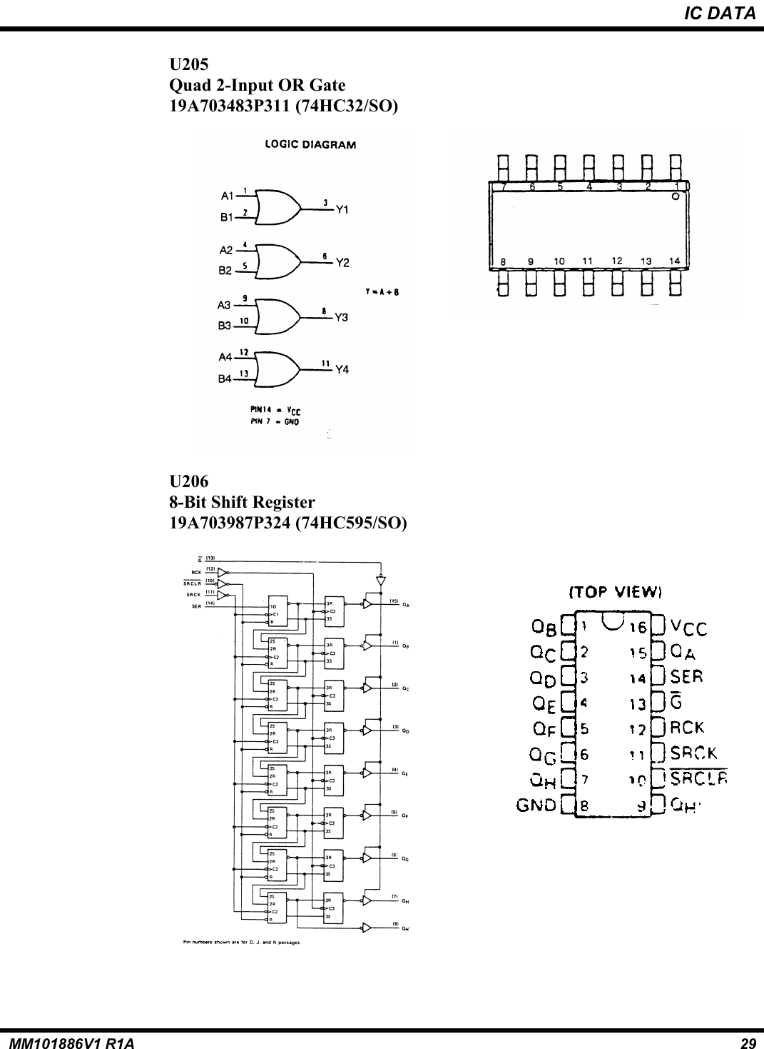
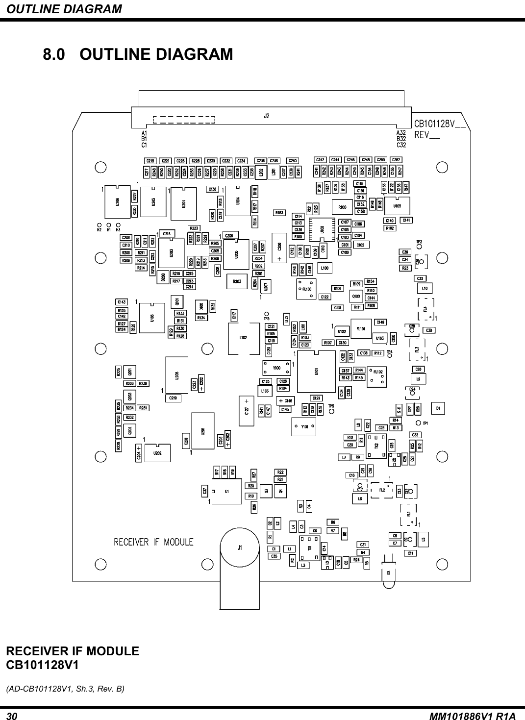
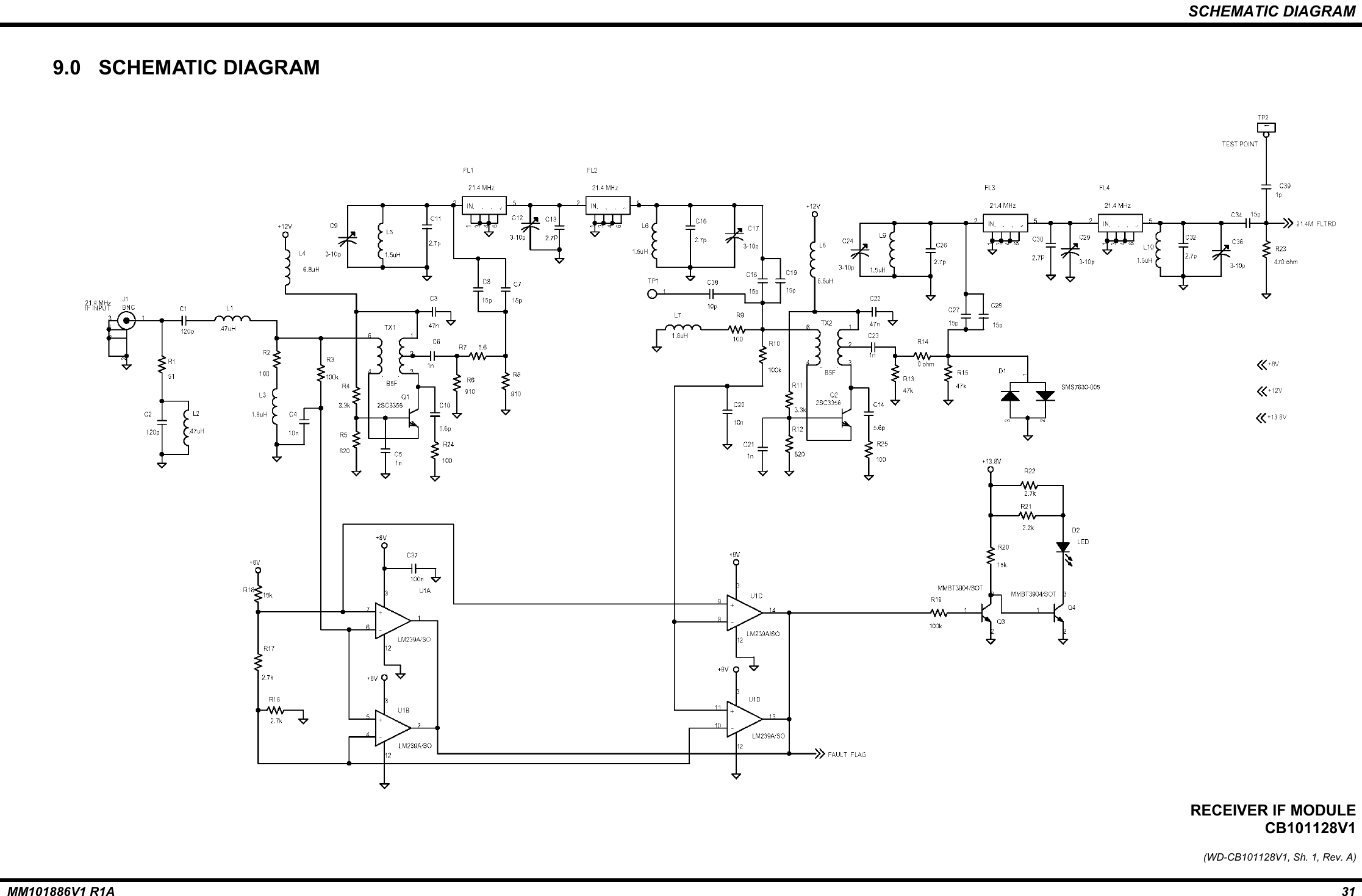
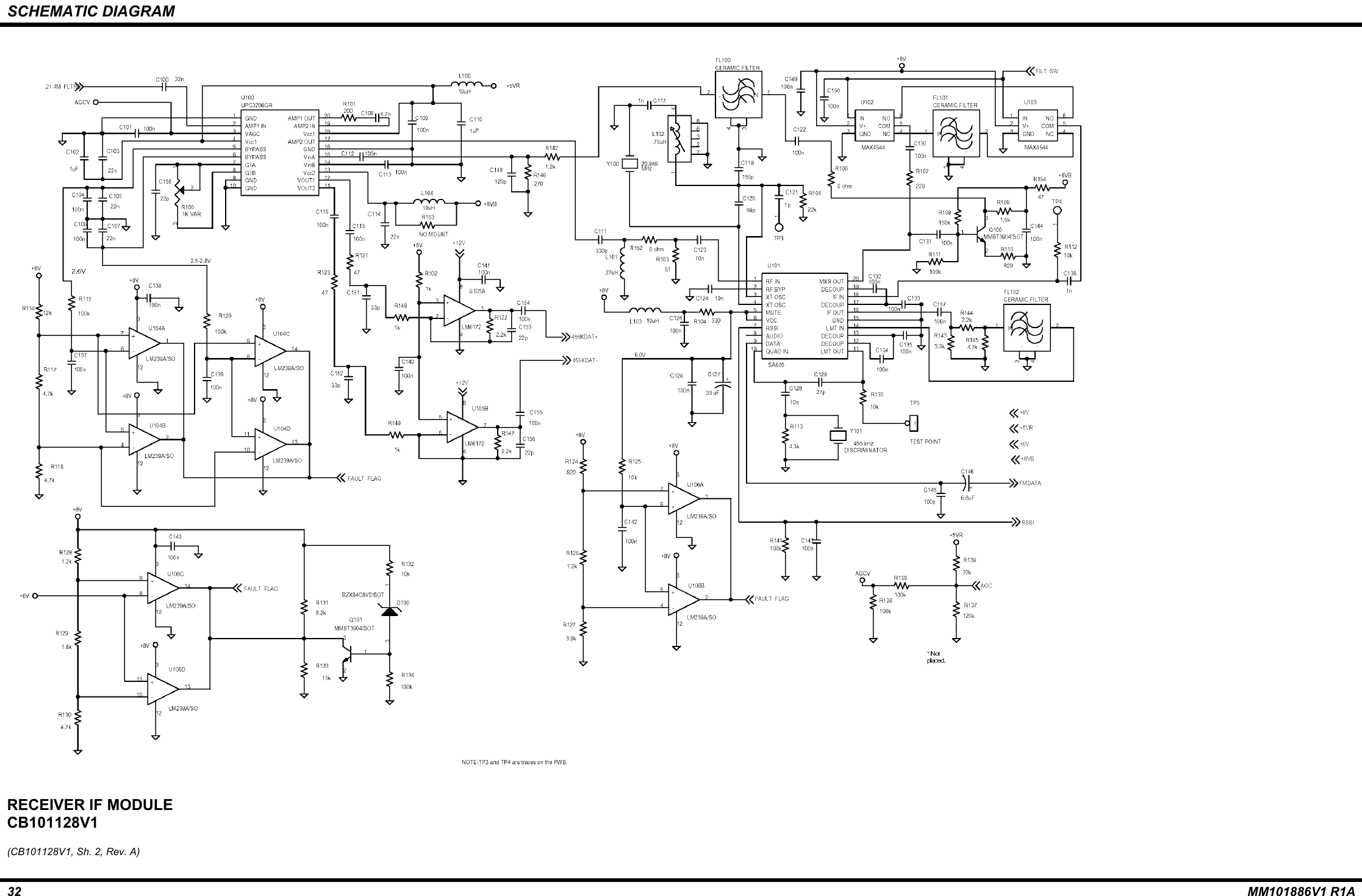
RX IF
6.
RX Synth
7.
TX Synth
8.
RF Package
9.
Site Pro Manual Part 1
10.
Site Pro Manual Part 2
RX IF
Navigation menu
Upload a User Manual
Namespaces
Wiki Guide
HTML
PDF
Info
Views
User Manual
Discussion / Help
Navigation