Nokia Solutions and Networks T5CS1 Cellular CDMA Base Station User Manual IHET5CS1 GLI2 4 of 4
Nokia Solutions and Networks Cellular CDMA Base Station IHET5CS1 GLI2 4 of 4
Contents
IHET5CS1 GLI2 User Manual 4 of 4
Test Equipment Preparation – continued
08/01/2001 F-5
1X SCt4812ET Lite BTS Optimization/ATP
PRELIMINARY
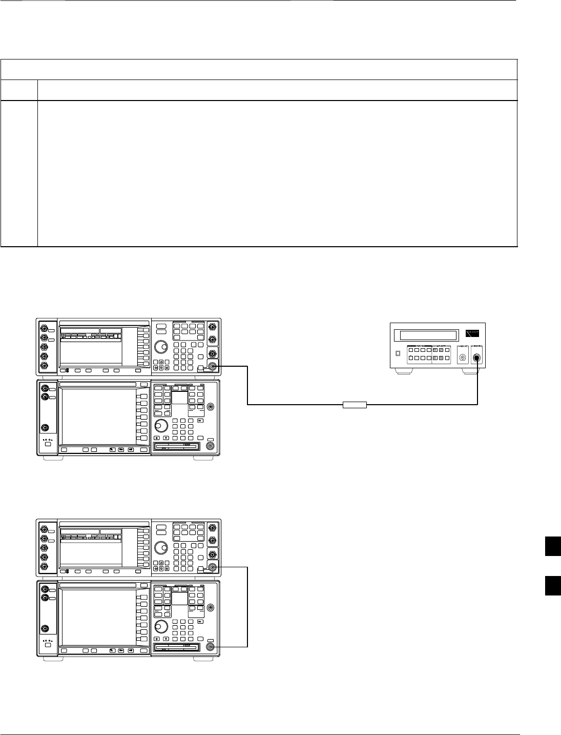
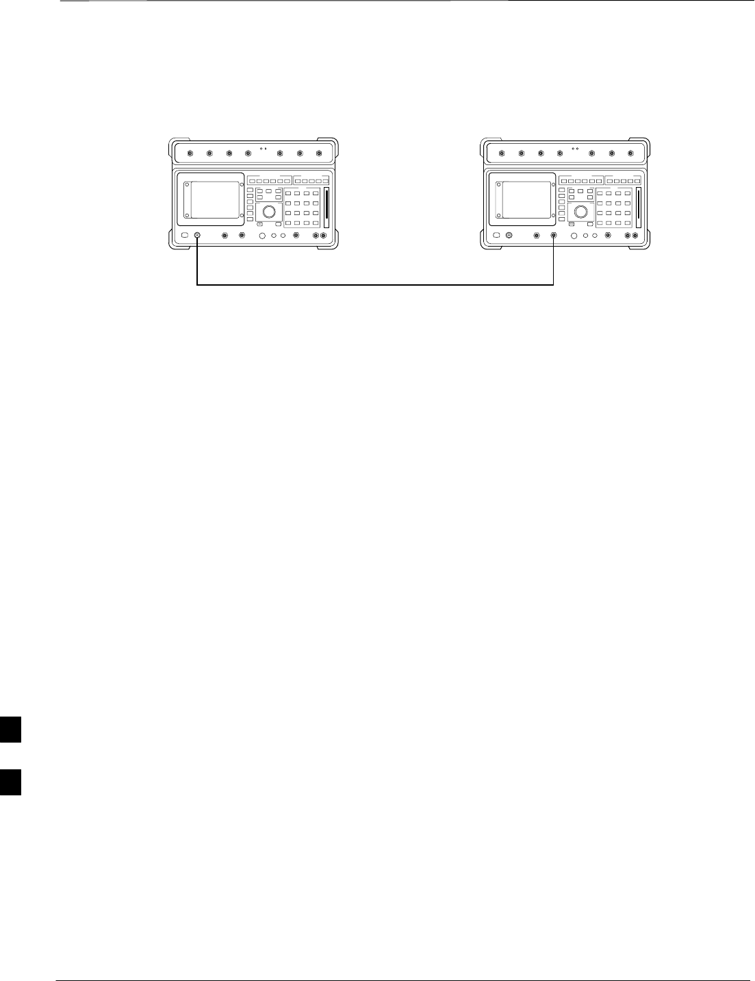
HP8921A System Connectivity
Test
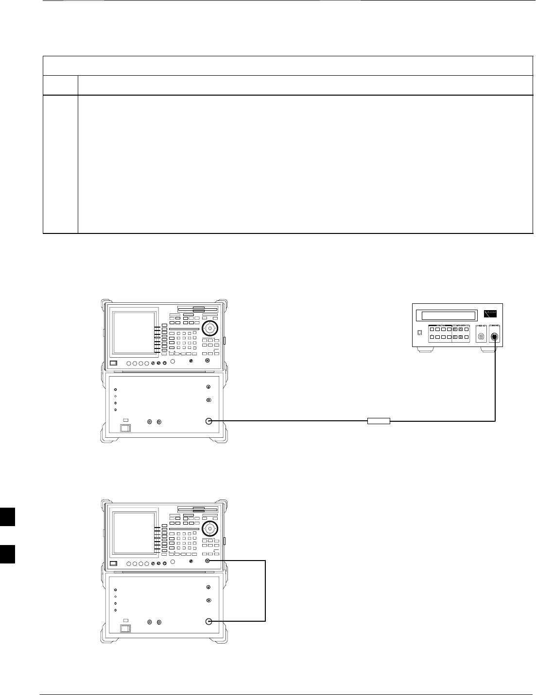
Follow the steps outlined in Table F-3 to verify that the connections
between the PCS Interface and the HP8921A are correct and cables are
intact. The software also performs basic functionality checks of each
instrument.
Disconnect other GPIB devices, especially system
controllers, from the system before running the
connectivity software.
IMPORTANT
*
Table F-3: System Connectivity
Step Action
* IMPORTANT
–Perform this procedure after test equipment has been allowed to warm–up and stabilize for a
minimum of 60 minutes.
1Insert HP 83236A Manual Control/System card into memory card slot.
2Press the [PRESET] pushbutton.
3Press the Screen Control [TESTS] pushbutton to display the “Tests” Main Menu screen.
4Position the cursor at Select Procedure Location and select it by pressing the cursor control knob. In
the Choices selection box, select Card.
5Position the cursor at Select Procedure Filename and select it by pressing the cursor control knob. In
the Choices selection box, select SYS_CONN.
6Position the cursor at RUN TEST and select it. The software will prompt you through the
connectivity setup.
7Do the following when the test is complete,
Sposition cursor on STOP TEST and select it
SOR press the [K5] pushbutton.
8To return to the main menu, press the [K5] pushbutton.
9Press the [PRESET] pushbutton.
F

Test Equipment Preparation – continued
PRELIMINARY
1X SCt4812ET Lite BTS Optimization/ATP 08/01/2001
F-6
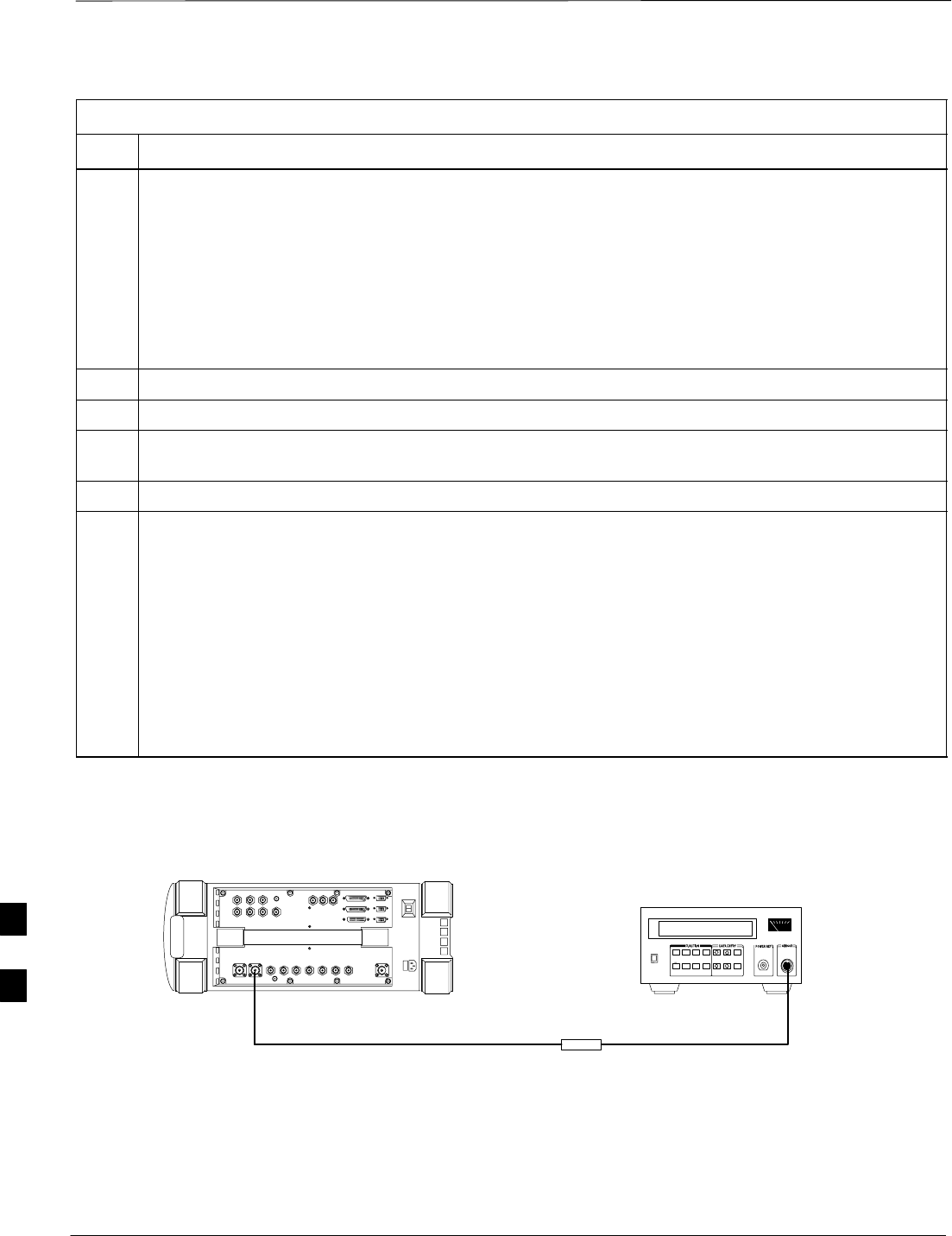
Setting HP8921A and
HP83236A/B GPIB Address
Table F-4: Setting HP8921A GPIB Address
Step Action
1If you have not already done so, turn the HP8921A power on.
2Verify that the GPIB addresses are set correctly.
SHP8921A HP–IB Adrs = 18, accessed by pushing LOCAL and selecting More and I/O Configure
on the HP8921A/600. (Consult test equipment OEM documentation for additional info as required).
SHP83236A (or B) PCS Interface GPIB address=19. Set dip switches as follows:
–A1=1, A2=1, A3=0, A4=0, A5=1, HP–IB/Ser = 1
Pretest Setup for HP8921A
Before the HP8921A CDMA analyzer is used for LMF controlled testing
it must be set up correctly for automatic testing.
Table F-5: Pretest Setup for HP8921A
Step Action
1Unplug the memory card if it is plugged in.
2Press the CURSOR CONTROL knob.
3Position the cursor at IO CONFIG (under To Screen and More) and select it.
4Select Mode and set for Talk&Lstn.
Pretest Setup for HP8935
Before the HP8935 CDMA analyzer is used for LMF controlled testing
it must be set up correctly for automatic testing.
Table F-6: Pretest Setup for HP8935
Step Action
1Unplug the memory card if it is plugged in.
2Press the Shift button and then press the I/O Config button.
3Press the Push to Select knob.
4Position the cursor at IO CONFIG and select it.
5 Select Mode and set for Talk&Lstn.
F
Test Equipment Preparation – continued
08/01/2001 F-7
1X SCt4812ET Lite BTS Optimization/ATP
PRELIMINARY
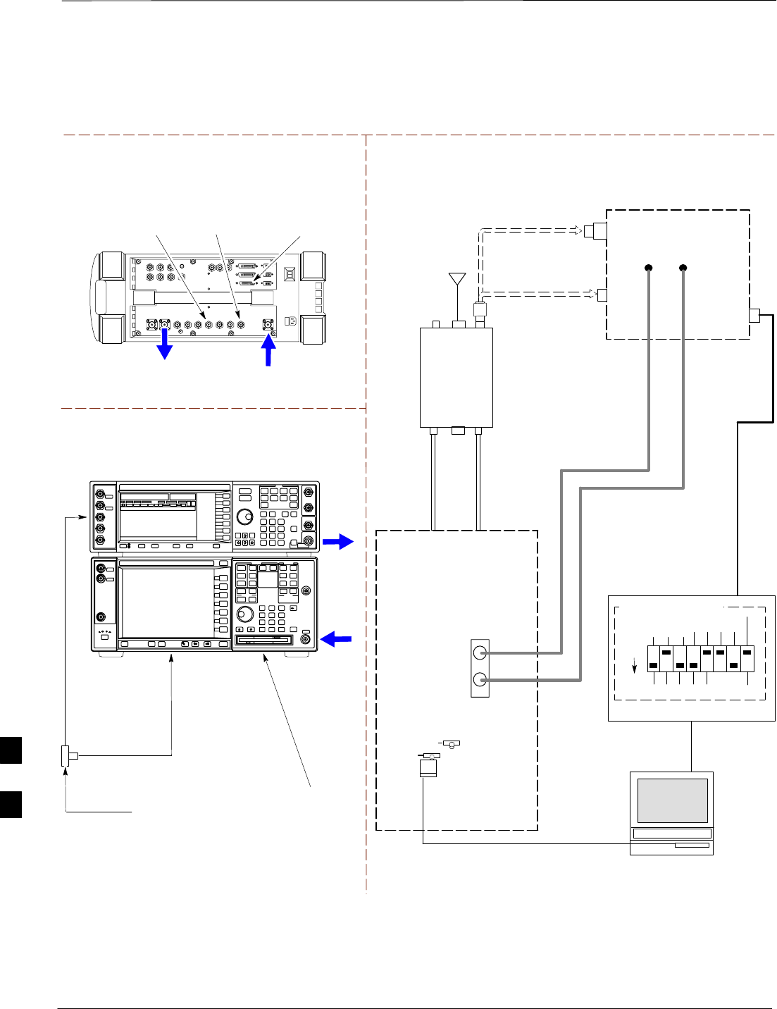
Advantest R3465 Connection
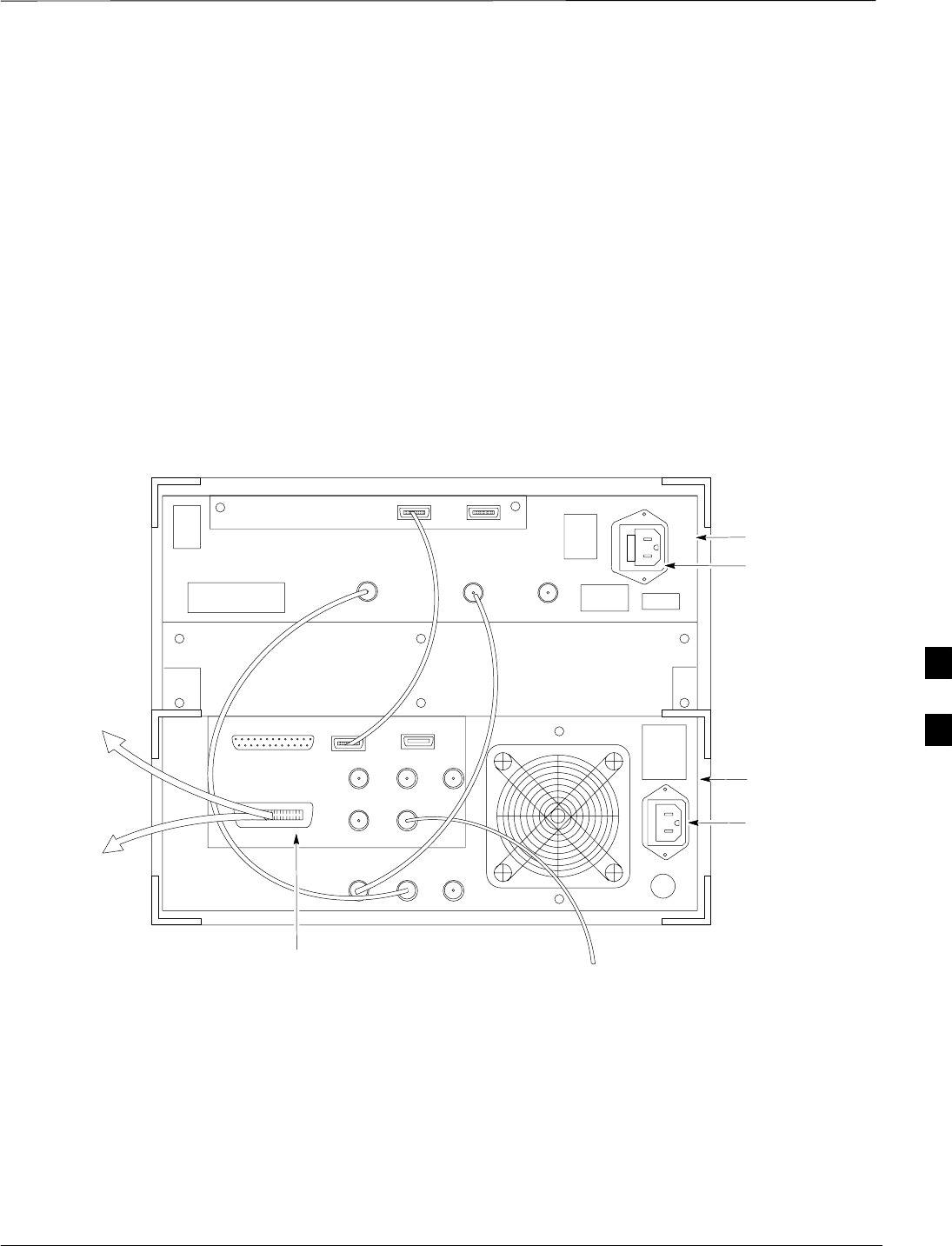
The following diagram depicts the rear panels of the Advantest test
equipment as configured to perform automatic tests. All test equipment
is controlled by the LMF via an IEEE–488/GPIB bus. The LMF expects
each piece of test equipment to have a factory-set GPIB address (refer to
Table F-7). If there is a communications problem between the LMF and
any piece of test equipment, you should verify that the GPIB addresses
have been set correctly and that the GPIB cables are firmly connected to
the test equipment.
Figure F-3 shows the connections when not using an external 10 MHz
Rubidium reference.
Figure F-3: Cable Connections for Test Set without 10 MHz Rubidium Reference
ADVANTEST R3465
REAR PANEL
GPIB
CONNECTOR
SERIAL I/O
LOCAL IN
SERIAL I/O
SYN REF IN 10 MHZ OUT
PARALLEL
EXT TRIGGER
10 MHZ REF
GATE IN
GPIB
CDMA CLOCK OUT
AC POWER
AC POWER
R3561L
REAR PANEL
R3465
REAR PANEL
TO T–CONNECTOR
ON FRONT PANEL
(EVEN/SEC/SYNC IN)
XYZ
IF OUT
421 MHZ
TO POWER METER
GPIB CONNECTOR
TO GPIB
INTERFACE BOX
FW00370
F
Test Equipment Preparation – continued
PRELIMINARY
1X SCt4812ET Lite BTS Optimization/ATP 08/01/2001
F-8
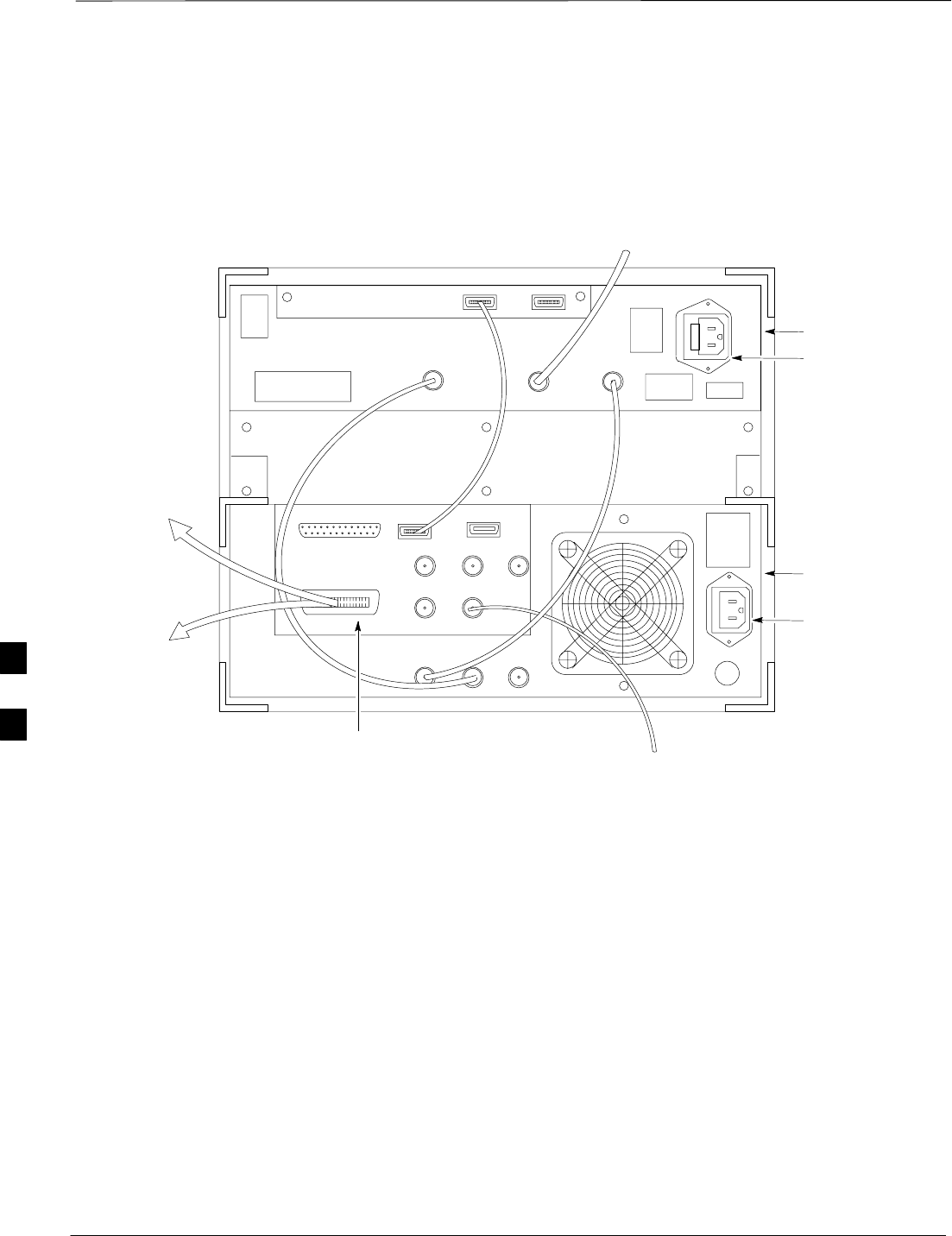
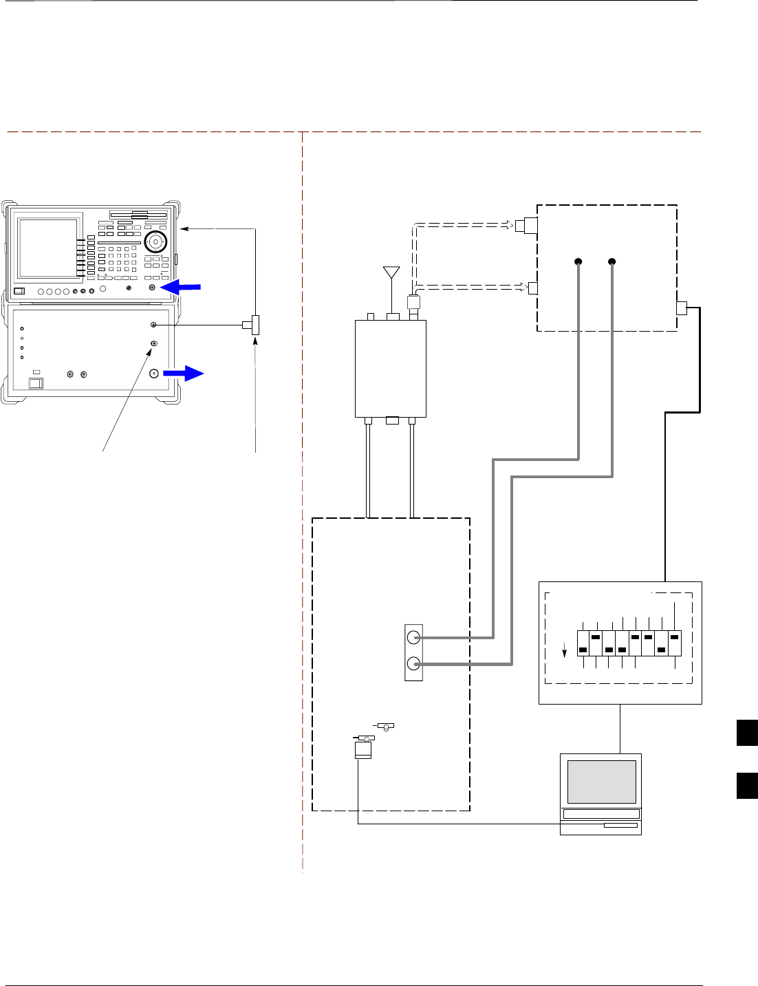
Figure F-4 shows the connections when using an external 10 MHz
Rubidium reference.
SERIAL I/O
GPIB
CONNECTOR ADVANTEST R3465
REAR PANEL
Figure F-4: Cable Connections for Test Set with 10 MHz Rubidium Reference
FROM 10 MHZ
RUBIDIUM REFERENCE
LOCAL IN
SERIAL I/O
IF OUT
SYN REF IN 10 MHZ OUT
PARALLEL
EXT TRIGGER
10 MHZ REF
GATE IN
GPIB
CDMA CLOCK OUT
AC POWER
AC POWER
R3465/3463
REAR PANEL
R3561L
REAR PANEL
TO T–CONNECTOR
ON FRONT PANEL
(EVEN SEC/SYNC IN)
XYZ
421 MHZ
TO POWER METER
GPIB CONNECTOR
TO GPIB
INTERFACE BOX
FW00371
F

Test Equipment Preparation – continued
08/01/2001 F-9
1X SCt4812ET Lite BTS Optimization/ATP
PRELIMINARY
R3465 GPIB Address & Clock
setup
Table F-7 describes the steps to set the GPIB address and clock for the
Advantest R3465 equipment.
Table F-7: Advantest R3465 GPIB Address and Clock Setup
Step Action
1Communications test set GPIB address=18 (perform the following to view/set as required)
Perform the following to set the standard parameters on the test set:
SPush the SHIFT then PRESET pushbutton (just below the CRT display).
SPush the LCL pushbutton (CW in Measurement just below the CRT display)
–Push the GPIB and Others CRT menu key to view the current address.
–If required, change GPIB address to 18 (rotate the vernier knob to set, push the vernier knob to
enter)
2Verify the current Date and Time in upper/right of the CRT display (perform the following to set if
required)
Communications test set GPIB address=18 (perform the following to view/set as required)
SPush the Date/Time CRT menu key
SIf required, change to correct Date/Time (rotate the vernier knob to select and set, push the vernier
knob to enter)
S Push the SHIFT then PRESET pushbutton (just below the CRT display).
Pretest Setup for Advantest
R3465
Before the Advantest R3465 analyzer is used for LMF controlled testing
it must be set up correctly for automatic testing.
Table F-8: Pretest Setup for Advantest R346
Step Action
1Press the SHIFT button so the LED next to it is illuminated.
2Press the RESET button.
F
Test Equipment Preparation – continued
PRELIMINARY
1X SCt4812ET Lite BTS Optimization/ATP 08/01/2001
F-10
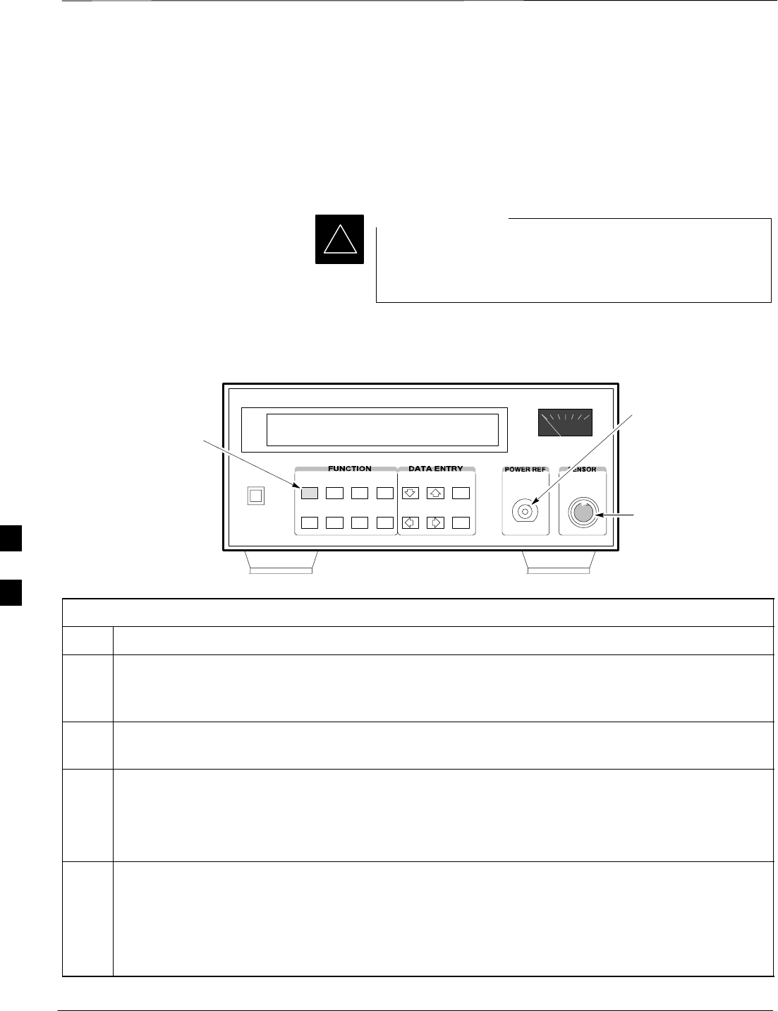
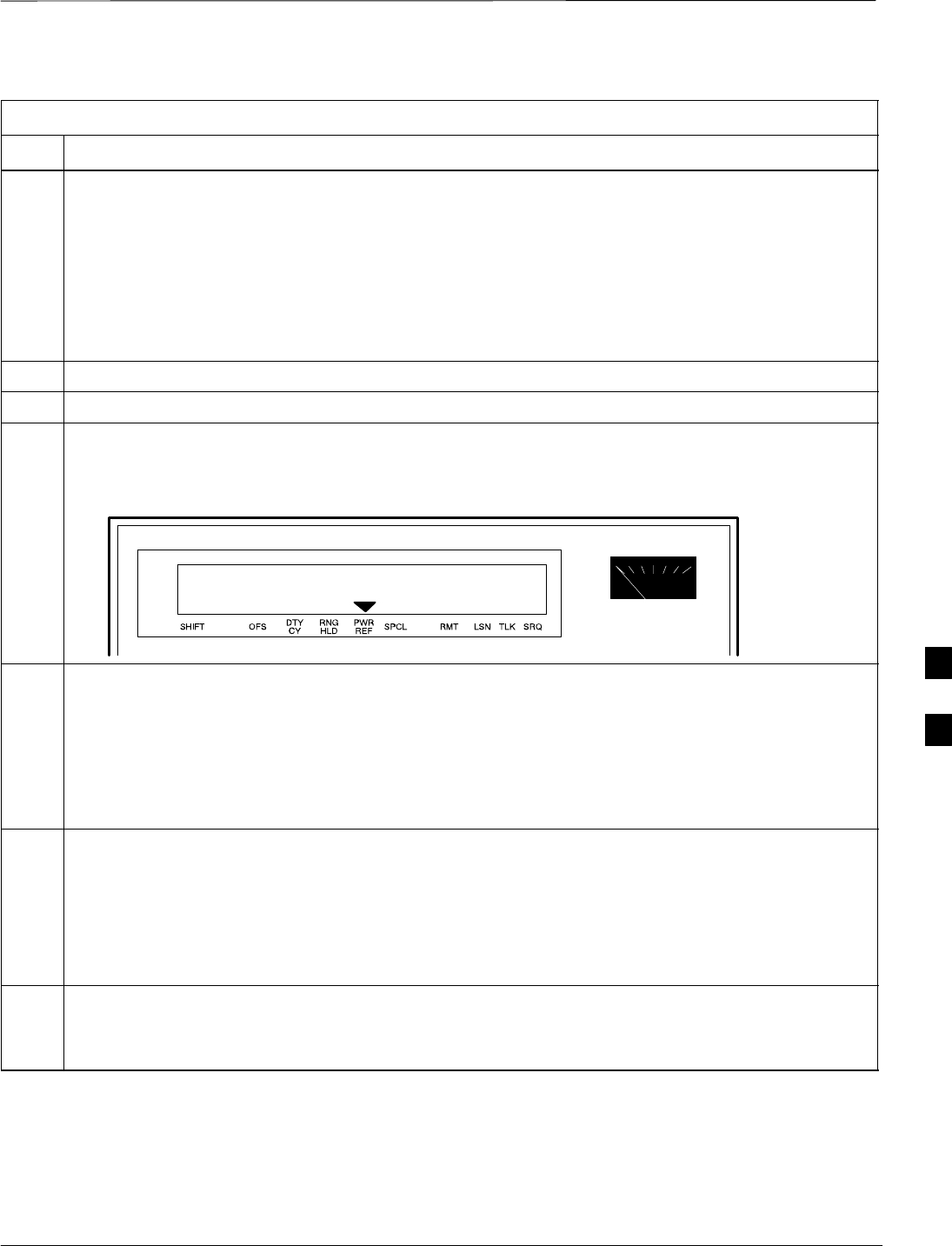
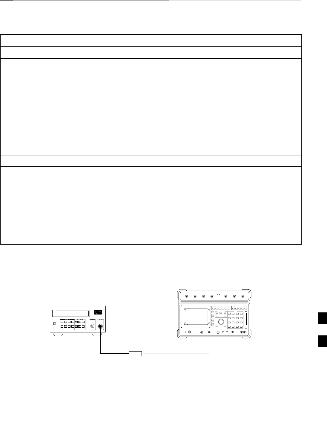
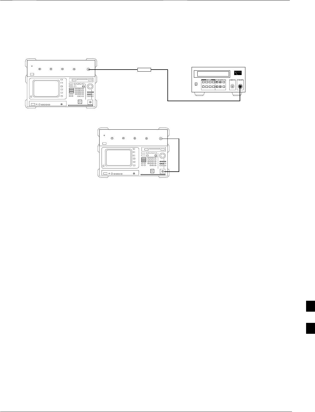
Calibrating HP437 Power Meter
Precise transmit output power calibration measurements are made using
a bolometer–type broadband power meter with a sensitive power sensor.
Follow the steps outlined in Table F-9 to enter information unique to the
power sensor before calibrating the test setup. Refer to Figure F-5 as
required.
This procedure must be done in conjunction with the
automated calibration to enter power sensor specific
calibration values.
IMPORTANT
*
CONNECT POWER
SENSOR WITH POWER
METER TURNED OFF
CONNECT POWER SENSOR
TO POWER REFERENCE
WHEN CALIBRATING UNIT.
POWER REFERENCE IS
ENABLED USING THE SHIFT '
KEYS
SHIFT (BLUE) PUSHBUTTON –
ACCESSES FUNCTION AND
DATA ENTRY KEYS IDENTIFIED
WITH LIGHT BLUE TEXT ON
THE FRONT PANEL ABOVE
THE BUTTONS
FW00308
Figure F-5: Power Meter Detail
Table F-9: Power Meter Calibration Procedure
Step Action
! CAUTION
Do not connect/disconnect the power meter sensor cable with ac power applied to the meter.
Disconnection could result in destruction of the sensing element or mis–calibration.
1–Make sure the power meter AC LINE pushbutton is OFF.
–Connect the power sensor cable to the SENSOR input.
2Set the AC LINE pushbutton to ON.
NOTE
The calibration should be performed only after the power meter and sensor have been allowed to
warm–up and stabilize for a minimum of 60 minutes.
3Perform the following to set or verify the GPIB address:
–To enter the SPECIAL data entry function, press [SHIFT] then [PRESET].
–Use the [y] or [b] button to select HP–IB ADRS; then press [ENTER].
–Use the [y] or [b] button to select HP–IB ADRS 13; then press [ENTER].
–To EXIT the SPECIAL data entry function press [SHIFT] then [ENTER].
. . . continued on next page
F
Test Equipment Preparation – continued
08/01/2001 F-11
1X SCt4812ET Lite BTS Optimization/ATP
PRELIMINARY
Table F-9: Power Meter Calibration Procedure
Step Action
4Perform the following to set or verify the correct power sensor model:
–Press [SHIFT] then [a] to select SENSOR.
–Identify the power sensor model number from the sensor label. Use the [y] or [b] button to
select the appropriate model; then press [ENTER].
NOTE
Be sure the PWR REF (power reference) output is OFF (observe that the triangular indicator is NOT
displayed as shown in Step 7). If on, press [SHIFT] then ['] to turn it off.
5 Press [ZERO]. Display will show “Zeroing ******.” Wait for process to complete.
6Connect the power sensor to the POWER REF output.
7To turn on the PWR REF, perform the following:
–Press [SHIFT] then ['].
–Verify that the triangular indicator (below) appears in the display above “PWR REF”.
8Perform the following to set the REF CF %:
–Press ([SHIFT] then [ZERO]) for CAL.
–Enter the sensor’s REF CF % from the sensor’s decal using the arrow keys and press [ENTER].
(The power meter will display ”CAL *****” for a few seconds.)
NOTE
If the REF CAL FACTOR (REF CF) is not shown on the power sensor, assume it to be 100%.
9Perform the following to set the CAL FAC %:
–Press [SHIFT] then [FREQ] for CAL FAC.
–On the sensor's decal, locate an approximate calibration percentage factor (CF%) at 2 GHz. Enter
the sensor’s calibration % (CF%) using the arrow keys and press [ENTER].
When complete, the power meter will typically display 0.05 dBm. (Any reading between 0.00 and
0.10 is normal.)
10 To turn off the PWR REF, perform the following:
–Press [SHIFT] then ['].
–Disconnect the power sensor from the POWER REF output.
F

Test Equipment Preparation – continued
PRELIMINARY
1X SCt4812ET Lite BTS Optimization/ATP 08/01/2001
F-12
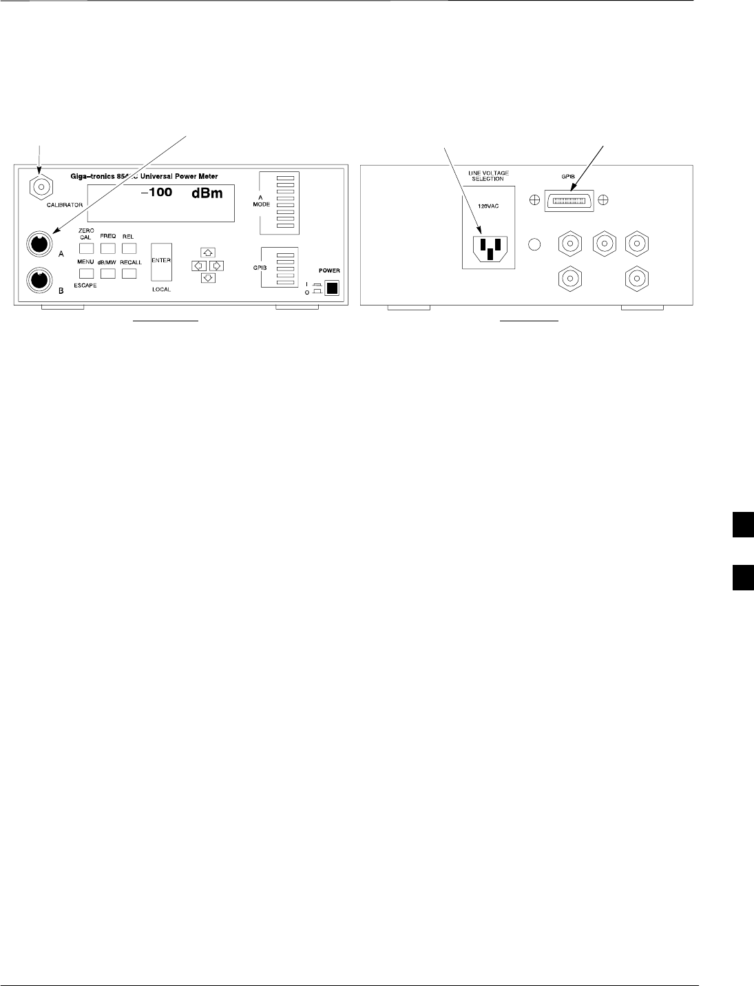
Calibrating Gigatronics 8542
power meter
Precise transmit output power calibration measurements are made using
a bolometer–type broadband power meter with a sensitive power sensor.
Follow the steps in Table F-10 to enter information unique to the power
sensor.
Table F-10: Calibrate Gigatronics 8542 Power Meter
Step Action
! CAUTION
Do not connect/disconnect the power meter sensor cable with AC power applied to the meter.
Disconnection could result in destruction of the sensing element or miscalibration.
NOTE
Allow the power meter and sensor to warm up and stabilize for a minimum of 60 minutes before
performing the calibration procedure.
1SMake sure the power meter POWER pushbutton is OFF.
SConnect the power sensor cable to the SENSOR input.
SSet the POWER pushbutton to ON.
2Verify the Power GPIB mode and address:
SPress MENU. Use the b arrow key to select CONFIG MENU, and press ENTER.
SUse the b arrow key to select GPIB, and press ENTER.
SUse the by arrow keys as required to set MODE to 8541C or 8542C (as appropriate).
SPress ' and use the by arrow keys as required to set ADDRESS to 13.
SPress ENTER.
3SConnect the power sensor to the CALIBRATOR output connector.
SPress ZERO.
SWait for the process to complete. Sensor factory calibration data is read to power meter during this
process.
SDisconnect the power sensor from the CALIBRATOR output.
F
Test Equipment Preparation – continued
08/01/2001 F-13
1X SCt4812ET Lite BTS Optimization/ATP
PRELIMINARY
Figure F-6: Gigatronics 8542C Power Meter Detail
CONNECT POWER SENSOR
WITH POWER METER
TURNED OFF
CONNECT POWER SENSOR TO
CALIBRATOR POWER REFERENCE
WHEN CALIBRATING/ZEROING UNIT
FRONT View REAR View
GPIB CONNECTIONAC POWER
FW00564
F

Manual Cable Calibration
PRELIMINARY
1X SCt4812ET Lite BTS Optimization/ATP 08/01/2001
F-14
Calibrating Test Cable Setup
using HP PCS Interface (HP83236)
Table F-11 covers the procedure to calibrate the test equipment using
the HP8921 Cellular Communications Analyzer equipped with the
HP83236 PCS Interface.
This calibration method must be executed with great care.
Some losses are measured close to the minimum limit of
the power meter sensor (–30 dBm).
NOTE
Prerequisites
Ensure the following prerequisites have been met before proceeding:
STest equipment to be calibrated has been connected correctly for cable
calibration.
STest equipment has been selected and calibrated.
Table F-11: Calibrating Test Cable Setup (using the HP PCS Interface)
Step Action
NOTE
Verify that GPIB controller is turned off.
1Insert HP83236 Manual Control System card into memory card slot.
2Press the Preset pushbutton.
3 Under Screen Controls, press the TESTS pushbutton to display the TESTS (Main Menu) screen.
4Position the cursor at Select Procedure Location and select it. In the Choices selection box, select
CARD.
5Position the cursor at Select Procedure Filename and select it. In the Choices selection box, select
MANUAL.
6Position the cursor at RUN TEST and select it. HP must be in Control Mode Select YES.
7If using HP83236A:
Set channel number=<chan#>:
–Position cursor at Channel
Number and select it.
–Enter the chan# using the numeric
keypad; press [Enter] and the
screen will go blank.
–When the screen reappears, the
chan# will be displayed on the
channel number line.
If using HP83236B:
Set channel frequency:
–Position cursor at Frequency Band and press Enter.
–Select User Defined Frequency.
–Go Back to Previous Menu.
–Position the cursor to 83236 generator frequency and
enter actual RX frequency.
–Position the cursor to 83236 analyzer frequency and
enter actual TX frequency.
. . . continued on next page
F

Manual Test Cable Setup – continued
08/01/2001 F-15
1X SCt4812ET Lite BTS Optimization/ATP
PRELIMINARY
Table F-11: Calibrating Test Cable Setup (using the HP PCS Interface)
Step Action
8Set RF Generator level:
–Position the cursor at RF Generator Level and select it.
–Enter –10 using the numeric keypad; press [Enter] and the screen will go blank.
–When the screen reappears, the value –10 dBm will be displayed on the RF Generator Level line.
9Set the user fixed Attenuation Setting to 0 dBm:
–Position cursor at Analyzer Attenuation and select it
–Position cursor at User Fixed Atten Settings and select it.
–Enter 0 (zero) using the numeric keypad and press [Enter].
10 Select Back to Previous Menu.
11 Record the HP83236 Generator Frequency Level:
Record the HP83236B Generator Frequency Level:
–Position cursor at Show Frequency and Level Details and select it.
–Under HP83236 Frequencies and Levels, record the Generator Level.
–Under HP83236B Frequencies and Levels, record the Generator Frequency Level (1850 – 1910
MHz).
–Position cursor at Prev Menu and select it.
12 Click on Pause for Manual Measurement.
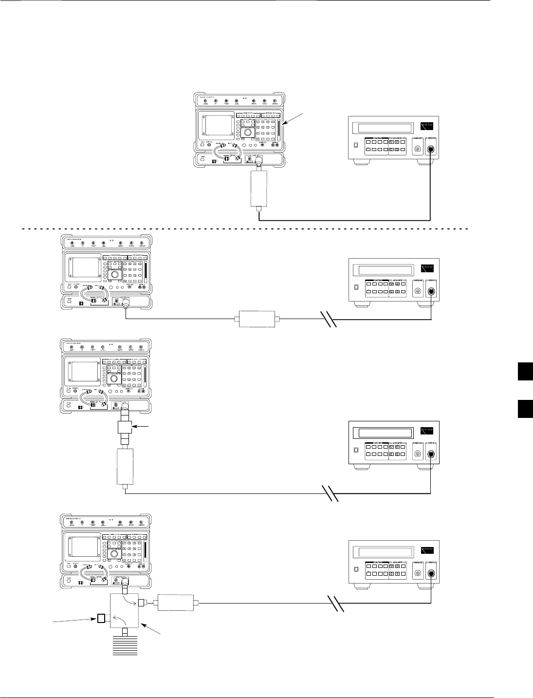
13 Connect the power sensor directly to the RF OUT ONLY port of the PCS Interface.
14 On the HP8921A, under To Screen, select CDMA GEN.
15 Move the cursor to the Amplitude field and click on the Amplitude value.
16 Increase the Amplitude value until the power meter reads 0 dBm ±0.2 dB.
NOTE
The Amplitude value can be increased coarsely until 0 dBM is reached; then fine tune the amplitude
by adjusting the Increment Set to 0.1 dBm and targeting in on 0 dBm.
17 Disconnect the power sensor from the RF OUT ONLY port of the PCS Interface.
* IMPORTANT
The Power Meter sensor’s lower limit is –30 dBm. Thus, only components having losses ≤30 dB
should be measured using this method. For further accuracy, always re-zero the power meter
before connecting the power sensor to the component being calibrated. After connecting the
power sensor to the component, record the calibrated loss immediately.
18 Disconnect all components in the test setup and calibrate each one separately by connecting each
component, one-at-a-time, between the RF OUT ONLY PORT and the power sensor. Record the
calibrated loss value displayed on the power meter.
SExample: (A) Test Cable(s) = –1.4 dB
(B) 20 dB Attenuator = –20.1 dB
(B) Directional Coupler = –29.8 dB
. . . continued on next page
F

Manual Test Cable Setup – continued
PRELIMINARY
1X SCt4812ET Lite BTS Optimization/ATP 08/01/2001
F-16
Table F-11: Calibrating Test Cable Setup (using the HP PCS Interface)
Step Action
19 After all components are calibrated, reassemble all components together and calculate the total test
setup loss by adding up all the individual losses:
SExample: Total test setup loss = –1.4 –29.8 –20.1 = –51.3 dB.
This calculated value will be used in the next series of tests.
20 Under Screen Controls press the TESTS button to display the TESTS (Main Menu) screen.
21 Select Continue (K2).
22 Select RF Generator Level and set to –119 dBm.
23 Click on Pause for Manual Measurement.
24 Verify the HP8921A Communication Analyzer/83203A CDMA interface setup is as follows (fields
not indicated remain at default):
SVerify the GPIB (HP–IB) address:
–under To Screen, select More
–select IO CONFIG
–Set HP–IB Adrs to 18
–set Mode to Talk&Lstn
SVerify the HP8921A is displaying frequency (instead of RF channel)
–Press the blue [SHIFT] button, then press the Screen Control [DUPLEX] button; this switches to
the CONFIG (CONFIGURE) screen.
–Use the cursor control to set RF Display to Freq
25 Refer toChapter 3 for assistance in setting the cable loss values into the LMF.
F
Manual Test Cable Setup – continued
08/01/2001 F-17
1X SCt4812ET Lite BTS Optimization/ATP
PRELIMINARY
(A)
(C)
POWER
SENSOR
(A)
POWER
SENSOR
(C)
30 dB
DIRECTIONAL
COUPLER
150 W
NON–RADIATING
RF LOAD
POWER
SENSOR
(B)
POWER
SENSOR
(B)
MEMORY
CARD
SLOT
20 dB / 20 WATT
ATTENUATOR
FW00292
Figure F-7: Cable Calibration Using HP8921 with PCS Interface
50 Ω
TERMINATION
F

Manual Test Cable Setup – continued
PRELIMINARY
1X SCt4812ET Lite BTS Optimization/ATP 08/01/2001
F-18
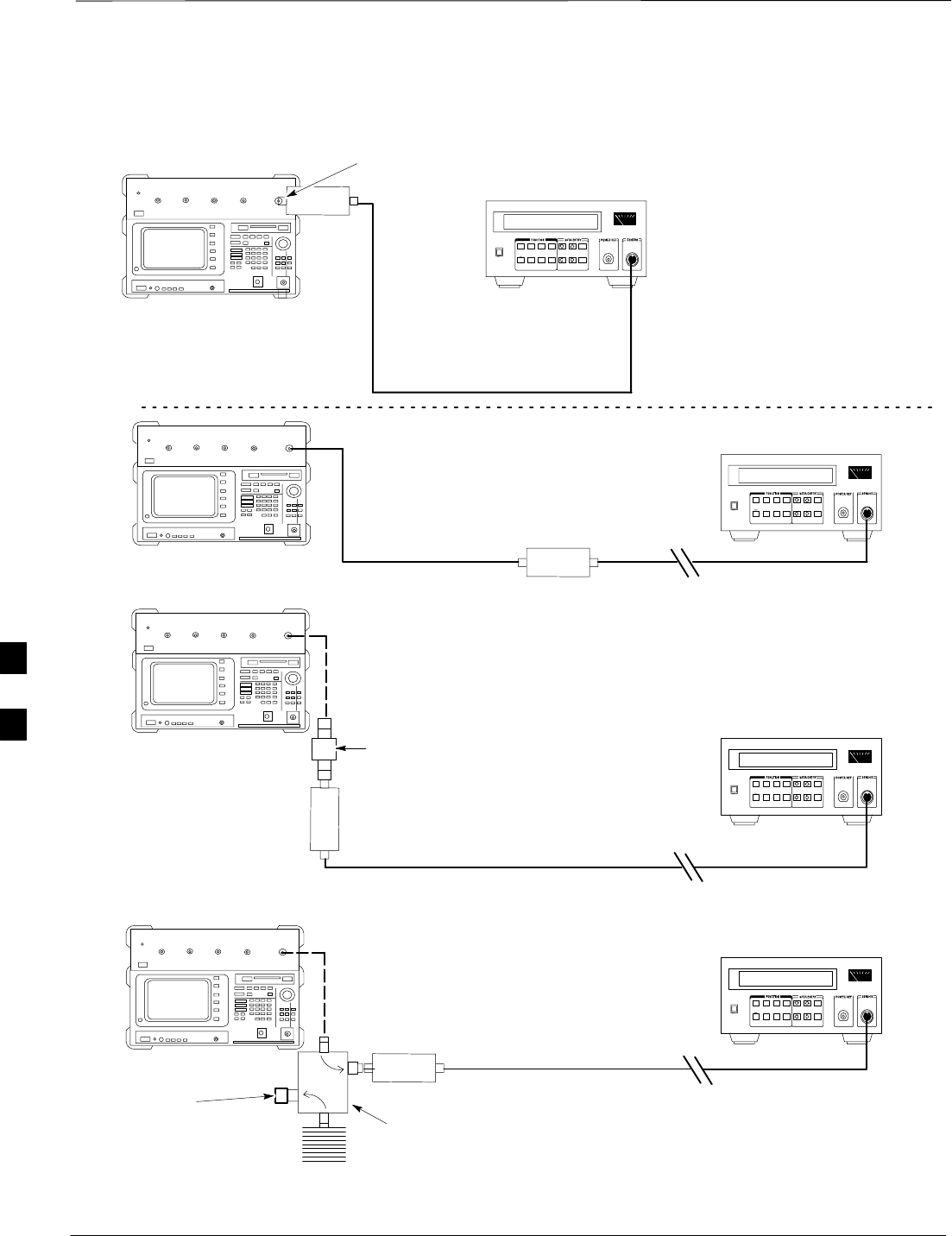
Calibrating Test Cable Setup
using Advantest R3465
Be sure the GPIB Interface is OFF for this procedure.
NOTE
Advantest R3465 Manual Test setup and calibration must be performed
at both the TX and RX frequencies.
Table F-12: Procedure for Calibrating Test Cable Setup Using Advantest R3465
Step Action
* IMPORTANT
–This procedure can only be performed after test equipment has been allowed to warm–up and
stabilize for a minimum of 60 minutes.
1Press the SHIFT and the PRESET keys located below the display
2Press the ADVANCE key in the MEASUREMENT area of the control panel.
3Select the CDMA Sig CRT menu key
4Select the Setup CRT menu key
5Using the vernier knob and the cursor keys set the following parameters
NOTE
Fields not listed remain at default
Generator Mode: SIGNAL
Link: FORWARD
Level Unit: dBm
CalCorrection: ON
Level Offset: OFF
6Select the return CRT menu key
7 Press FREQ key in the ENTRY area
8Set the frequency to the desired value using the keypad entry keys
9Verify that the Mod CRT menu key is highlighting OFF; if not, press the Mod key to toggle it OFF.
10 Verify that the Output CRT menu key is highlighting OFF; if not, press the Output key to toggle it
OFF.
11 Press the LEVEL key in the ENTRY area.
12 Set the LEVEL to 0 dBm using the key pad entry keys.
13 Zero power meter. Next connect the power sensor directly to the “RF OUT” port on the R3561L
CDMA Test Source Unit.
14 Press the Output CRT menu key to toggle Output to ON.
15 Record the power meter reading ________________________
. . . continued on next page
F

Manual Test Cable Setup – continued
08/01/2001 F-19
1X SCt4812ET Lite BTS Optimization/ATP
PRELIMINARY
Table F-12: Procedure for Calibrating Test Cable Setup Using Advantest R3465
Step Action
16 Disconnect the power meter sensor from the R3561L RF OUT jack.
* IMPORTANT
The Power Meter sensor’s lower limit is –30 dBm. Thus, only components having losses < 30 dB
should be measured using this method. For best accuracy, always re–zero the power meter before
connecting the power sensor to the component being calibrated. Then, after connecting the
power sensor to the component, record the calibrated loss immediately.
17 Disconnect all components in the the test setup and calibrate each one separately. Connect each
component one–at–a–time between the “RF OUT” port and the power sensor (see Figure F-8, “Setups
A, B, and C”). Record the calibrated loss value displayed on the power meter for each connection.
Example: (A) 1st Test Cable = –0.5 dB
(B) 2nd Test Cable = –1.4 dB
(C) 20 dB Attenuator = –20.1 dB
(D) 30 dB Directional Coupler = –29.8 dB
18 Press the Output CRT menu key to toggle Output OFF.
19 Calculate the total test setup loss by adding up all the individual losses:
Example: Total test setup loss = 0.5 + 1.4 + 20.1 + 29.8 = 51.8 dB
This calculated value will be used in the next series of tests.
20 Press the FREQ key in the ENTRY area
21 Using the keypad entry keys, set the test frequency to the RX frequency
22 Repeat steps 9 through 19 for the RX frequency.
23 Refer to Chapter 3 for assistance in setting the cable loss values into the LMF.
F
Manual Test Cable Setup – continued
PRELIMINARY
1X SCt4812ET Lite BTS Optimization/ATP 08/01/2001
F-20
POWER
SENSOR
20 DB / 2 WATT
ATTENUATOR
(A)
(C)
POWER
SENSOR
(D)
30 DB
DIRECTIONAL
COUPLER
(C)
100 W
NON–RADIATING
RF LOAD
POWER
SENSOR
RF OUT
POWER
SENSOR
& (B)
FW00320
Figure F-8: Cable Calibration Using Advantest R3465
50 Ω
TERMINATION
F

08/01/2001 1X SCt4812ET Lite BTS Optimization/ATP
PRELIMINARY
Appendix G: Download ROM Code
Appendix Content
Downloading ROM Code with the LMF G-1. . . . . . . . . . . . . . . . . . . . . . . . . . . . . .
Exception Procedure – Downloading Device ROM Code G-1. . . . . . . . . .
F

Table of Contents – continued
PRELIMINARY
1X SCt4812ET Lite BTS Optimization/ATP 08/01/2001
Notes
F
Downloading ROM Code with the LMF
08/01/2001 G-1
1X SCt4812ET Lite BTS Optimization/ATP
PRELIMINARY
Exception Procedure –
Downloading Device ROM
Code
This procedure is not part of a normal optimization.
Perform this procedure only on an exception basis when no alternative
exists to load a BTS device with the correct version of ROM code.
An MGLI or GLI must be INS (green) before ROM code
can be downloaded to non–GLI devices.
NOTE
Release 2.9.x RAM code must NOT be downloaded to a
device loaded with Release 2.8.x ROM code, and Release
2.8.x RAM code must NOT be downloaded to a device
loaded with Release 2.9.x ROM code.
All devices in a BTS must have the same Release–level
ROM and RAM code before the optimization and ATP
procedures can be performed.
If a newly–installed Release 8–equipped BTS is to be
upgraded to Release 2.9.x, the optimization and
Acceptance Test Procedures (ATP) should be accomplished
with the Release 2.8.x code and software. Following the
optimization, the site code and software should be
upgraded to Release 2.9.x by the CBSC. It is not necessary
to perform the optimization and ATPs again after the
upgrade.
If a replacement device with Release 2.8.x ROM code
must be used in a Release 2.9.x–equipped BTS, the device
ROM code can be changed using the CDMA LMF before
the performing the BTS optimization and ATPs. A device
loaded with Release 2.9.x ROM code can not be converted
back to Release 2.8.x ROM code in the field without
Motorola assistance.
CAUTION
If it is necessary to download ROM code to a device from the CDMA
LMF, the procedure in Table G-1 includes steps for both ROM and RAM
code download using the CDMA LMF.
Prerequisites
Prior to performing this procedure, ensure the correct ROM and RAM
code files exist on the CDMA LMF for each of the devices to be loaded.
F
Downloading ROM Code with the LMF – continued
PRELIMINARY
1X SCt4812ET Lite BTS Optimization/ATP 08/01/2001
G-2
The Release level of the ROM code to be downloaded
must be the same as the Release level of the ROM code
resident in the other devices in the BTS. Release 2.9.x
ROM code must not be downloaded to a frame having
Release 2.8.x code, and Release 2.8.x code must not be
downloaded to a frame having Release 2.9.x code.
This procedure should only be used to upgrade
replacement devices for a BTS. It should NOT be used to
upgrade all devices in a BTS. If a BTS is to be upgraded
from Release 2.8.x to Release 2.9.x, optimization and ATP
must first be performed with the BTS in a Release 2.8.x
configuration. Following this, the upgrade from Release
2.8.x to Release 2.9.x should be done by the CBSC.
CAUTION
Table G-1: Download ROM and RAM Code to Devices
Step Action
1Click on the device to be loaded.
2From the Device pull down menu, select Status.
A status report window will appear
3Make a note of the number in the HW Bin Type column.
NOTE
“HW Bin Type” is the Hardware Binary Type for the device. This number is used as the last four digits
in the filename of a device’s binary ROM code file. Using this part of the filename, the ROM code file
can be matched to the device in which it is to be loaded.
4 Click OK to close the status window.
5Click on the device to be loaded.
* IMPORTANT
The CDMA LMF will not automatically select ROM code files for download. ROM code files must
be selected manually.
6From the Device pull down menu, select Download Code Manual.
A file selection window will appear.
7 Double–click on the version folder with the desired version number for the ROM code file.
8 Double–click the Code folder.
A list of ROM and RAM code files will be displayed.
. . . continued on next page
F

Downloading ROM Code with the LMF – continued
08/01/2001 G-3
1X SCt4812ET Lite BTS Optimization/ATP
PRELIMINARY
Table G-1: Download ROM and RAM Code to Devices
Step Action
! CAUTION
A ROM code file with the correct hardware binary type (HW Bin Type) must be chosen. Using a file
with the wrong HW Bin Type can result in unpredictable operation and damage to the device.
9Click on the ROM code file with the filename which matches the device type and HW Bin Type
number noted in step 3 (e.g., file bbx_rom.bin.0604 is the ROM code file for a BBX with a HW Bin
Type of 0604).
The file should be highlighted.
10 Click on the Load button.
A status report window is displayed showing the result of the download.
11 Click OK to close the status window.
12 From the Util pull down menu, select Tools, then Update NextLoad.
13 Select the version number of the folder that was used for the ROM code download and click Save.
A pop–up message will appear showing the CDF file has been updated.
14 Click on the OK button to dismiss the pop–up message.
15 Click on the device that was loaded with ROM code.
NOTE
RAM code is automatically selected for download.
16 From the Device pull down menu, select Download Code to download RAM code.
A status report is displayed showing the result of the download.
17 Click OK to close the status window.
18 Observe the downloaded device to ensure it is OOS–RAM (yellow) for non–GLI devices or INS
(green) for GLIs.
19 Click on the device which was loaded with code.
20 From the Device pull down menu, select Status.
Verify that the correct ROM and RAM version numbers are displayed in the status report window.
21 Click OK to close the status window.
NOTE
Data is automatically downloaded to GLI devices when the RAM code is downloaded. Use the data
download portion of the Download RAM Code and Data to Non–GLI Devices procedure, Table 3-15,
to download data to other device types after their ROM code has been upgraded and RAM code
downloaded.
F

Downloading ROM Code with the LMF – continued
PRELIMINARY
1X SCt4812ET Lite BTS Optimization/ATP 08/01/2001
G-4
Notes
F

08/01/2001 1X SCt4812ET Lite BTS Optimization/ATP
PRELIMINARY
Appendix H: In–Service Calibration
Appendix Content
Introduction H-1. . . . . . . . . . . . . . . . . . . . . . . . . . . . . . . . . . . . . . . . . . . . . . . . . . . . .
Purpose H-1. . . . . . . . . . . . . . . . . . . . . . . . . . . . . . . . . . . . . . . . . . . . . . . . .
Equipment Warm up H-1. . . . . . . . . . . . . . . . . . . . . . . . . . . . . . . . . . . . . . .
1X Test Equipment Requirements H-1. . . . . . . . . . . . . . . . . . . . . . . . . . . . .
Power Delta Calibration H-3. . . . . . . . . . . . . . . . . . . . . . . . . . . . . . . . . . . . . . . . . . .
Power Delta Calibration Introduction H-3. . . . . . . . . . . . . . . . . . . . . . . . . .
Agilent E4406A Power Delta Calibration H-3. . . . . . . . . . . . . . . . . . . . . . .
Advantest R3267 Power Delta Calibration H-6. . . . . . . . . . . . . . . . . . . . . .
Agilent 8935 series E6380A Power Delta Calibration H-9. . . . . . . . . . . . .
HP8921A Power Delta Calibration H-12. . . . . . . . . . . . . . . . . . . . . . . . . . . .
Advantest R3465 Power Delta Calibration H-15. . . . . . . . . . . . . . . . . . . . . .
In–Service Calibration H-18. . . . . . . . . . . . . . . . . . . . . . . . . . . . . . . . . . . . . . . . . . . .
In–Service Calibration for 1X Upgrade H-18. . . . . . . . . . . . . . . . . . . . . . . . .
H

Table of Contents – continued
PRELIMINARY
1X SCt4812ET Lite BTS Optimization/ATP 08/01/2001
Notes
H
Introduction
08/01/2001 H-1
1X SCt4812ET Lite BTS Optimization/ATP
PRELIMINARY
Purpose
This procedure is a guide to performing calibration of new BTS
expansion carriers while the system remains in service. This procedure
also supports BTS recalibration following replacement of RF chain
components while the remainder of the site stays in service.
Motorola recommends performing this procedure during a maintenance
window.
This procedure cannot be performed on BTSs with 2–to–1 combiners.
The procedure can only be performed on one side of the BTS at one
time. That is, LPAs 1A, 1B, 1C, and 1D can be calibrated while LPAs
3A, 3B, 3C, and 3D remain in service and vice versa.
Equipment Warm up
Calibration of the communications test set (or equivalent
test equipment) must be performed at the site before
calibrating the overall test equipment set. Calibrate the test
equipment after it has been allowed to warm-up and
stabilize for a minimum of 60 minutes.
IMPORTANT
*
If any component of the test equipment set (for example, a
test cable, RF adapter, signal generator) has been replaced,
the test equipment set must be recalibrated. Failure to do so
could introduce measurement errors which ultimately result
in degradation of system performance.
CAUTION
1X Test Equipment
Requirements
Calibration of 1X carrier functions requires using either of the following
test equipment combinations:
SAn Advantest R3267 spectrum analyzer with an Advantest R3562
signal generator
SAn Agilent E4406A Transmitter Test Set with an Agilent E4432A
signal generator
SAn Agilent 8935 series E6380A equipped with option 200 (if
purchased new) or option R2K (if retrofitted) and an Agilent E4432B
signal generator
These test equipment combinations are capable of calibrating the BTS
for both IS–95 A and B mode operation as well as IS–2000 CDMA 1X
operation.
H

Introduction – continued
PRELIMINARY
1X SCt4812ET Lite BTS Optimization/ATP 08/01/2001
H-2
IS–95A/B communication test sets such as the
HP8921A/600 and Advantest R3561L can not calibrate 1X
carrier functions.
IMPORTANT
*
Calibration and test set–up for the HP 8921A/600 and Advantest
R3561L test sets is included only for situations where it is necessary to
use them for calibration of IS–95A/B mode operation.
H

Power Delta Calibration
08/01/2001 H-3
1X SCt4812ET Lite BTS Optimization/ATP
PRELIMINARY
Power Delta Calibration
Introduction
The ISC procedure has several differences from a normal calibration
procedure. One of these is the use of a spectrum
analyzer/communications test set instead of a power meter to measure
power. Power meters are broadband measurement devices and cannot be
used to measure power during ISC because other carriers are operating.
A spectrum analyzer can be used because it measures power at a given
frequency. Measuring power using a spectrum analyzer is less accurate
than using a power meter, therefore, compensation is required for the
accuracy difference (delta) between the power meter and the spectrum
analyzer.
Agilent E4406A Power Delta
Calibration
The Agilent E4406A transmitter tester and E4432B signal generator test
equipment combination can be used for ISC of IS–2000 CDMA 1X as
well as IS–95A/B operation modes. The power delta calibration is
performed on the E4406A, but the E4432B is required to generate the
reference signal used to calculate the power delta offset. After the offset
value has been calculated, add it to the TX cable loss value in the LMF.
Follow the procedure in Table H-1 to perform the Agilent E4406A
Power Delta Calibration procedure.
Table H-1: Agilent E4406A Power Delta Calibration Procedure
Step Action
* IMPORTANT
Perform this procedure after test equipment has been allowed to warm–up and stabilize for a minimum
of 60 minutes. After it is warmed up and stabilized, calibrate the test equipment as described in the
“Test Set Calibration” section of Chapter 3.
1Zero the Power Meter prior to connecting the power sensor to the RF cable from the signal generator.
* IMPORTANT
For best accuracy, always re–zero the power meter before connecting the power sensor to the
component being calibrated.
2Connect a short RF cable from the E4432B RF OUTPUT connector the HP437 power meter power
sensor (see Figure H-1).
3Set the E4432B signal generator as follows:
–Press Preset to exit any modes for which the signal generator is configured
–Press Frequency and enter the frequency of the channel to be calibrated on the numeric keypad
–Using the soft keys to the right of the screen, select the frequency range to be measured; for
example MHz
–Press Amplitude and, using the numeric keypad, set signal amplitude to 0 (zero)
–Using the soft keys, set the measurement type to dBm
. . . continued on next page
H

Power Delta Calibration – continued
PRELIMINARY
1X SCt4812ET Lite BTS Optimization/ATP 08/01/2001
H-4
Table H-1: Agilent E4406A Power Delta Calibration Procedure
Step Action
4On the E4432B, press RF On/Off to toggle the RF output to RF ON.
–Note that the RF On/Off status in the screen display changes.
5Measure and record the value reading on the HP437 power meter as result A____________________.
6On the E4432B, press RF On/Off to toggle the RF output to RF OFF.
–Note that the RF On/Off status in the screen display changes.
7Disconnect the short RF cable from the HP437 power meter power sensor, and connect it to the RF
INPUT connector on the E4406A transmitter tester (see Figure H-2).
8* IMPORTANT
Do not change the frequency and amplitude settings on the E4432B when performing the following
steps.
Set the E4406A as follows:
–Press Preset to exit any modes for which the transmitter tester is configured
–Press MODE and, using the soft keys to the right of the screen, select cdmaOne
–Press MEASURE and, using the soft keys, select spectrum
–Press Frequency and, using the soft keys, select Center Frequency
–Enter the frequency of the channel to be calibrated using the numeric keypad
–Using the soft keys, select the frequency range to be measured; for example, MHz
–Press Input/Output and, using the soft keys, select Input Atten
–Using the numeric keypad, set Input Atten to 0 (zero) and, using the soft keys, select dB
–Using the soft keys, select External Atten and then select Mobile
–Using the numeric keypad, set Mobile to 0 (zero) and, using the soft keys, select dB
–Using the soft keys, select Base
–Using the numeric keypad, set Base to 0 (zero) and, using the soft keys, select dB
–Press MEASURE and, using the soft keys, select Channel Power
9On the E4432B signal generator, press RF On/Off to toggle the RF output to RF ON.
–Note that the RF On/Off status in the screen display changes.
10 Read the measured Channel Power from the E4406A screen display and record it as
result B____________________.
11 On the E4432B, press RF On/Off to toggle the RF output to RF OFF.
–Note that the RF On/Off status in the screen display changes.
. . . continued on next page
H
Power Delta Calibration – continued
08/01/2001 H-5
1X SCt4812ET Lite BTS Optimization/ATP
PRELIMINARY
Table H-1: Agilent E4406A Power Delta Calibration Procedure
Step Action
12 Calculate the Power Calibration Delta value. The delta value is the power meter measurement minus
the Agilent measurement.
Delta = A – B
Example: Delta = –0.70 dBm – (–1.25 dBm) = 0.55 dBm
Example: Delta = 0.26 dBm – 0.55 dBm = –0.29 dBm
These examples are included to show the mathematics and do not represent actual readings.
NOTE
Add this delta value to the TX Cable Loss value during In–Service Calibration (see step 4 in
Table H-6).
Figure H-1: Delta Calibration Setup – Agilent E4432B to HP437
Power
Sensor
Agilent E4432B and E4406A
Short RF Cable
HP437B
SENSOR
RF OUTPUT
Figure H-2: Delta Calibration Setup – Agilent E4432B to Agilent E4406A
Short RF Cable
RF INPUT
Agilent E4432B and E4406A
RF OUTPUT H

Power Delta Calibration – continued
PRELIMINARY
1X SCt4812ET Lite BTS Optimization/ATP 08/01/2001
H-6
Advantest R3267 Power Delta
Calibration
The Advantest R3267 spectrum analyzer and R3562 signal generator test
equipment combination can be used for ISC of IS–2000 CDMA 1X as
well as IS–95A/B operation modes. The power delta calibration is
performed on the R3267. After the offset value has been calculated, add
it to the TX cable loss value.
Follow the procedure in Table H-2 to perform the Advantest R3267
Power Delta Calibration procedure.
Table H-2: Advantest R3267 Power Delta Calibration Procedure
Step Action
1* IMPORTANT
Warm-up test equipment for a minimum of 60 minutes prior to this procedure. After it is warmed up
and stabilized, calibrate the test equipment as described in the “Test Set Calibration” section of
Chapter 3.
Press the SHIFT and the PRESET keys located on the right side of the control panel.
2Press the ADVANCE key in the MEASUREMENT area of the control panel.
3On the CRT, select RX Control by pressing ACTIVE key 1.
4On the CRT, select Frequency Setup by pressing ACTIVE key 3.
5On the CRT, highlight Frequency by adjusting the DISPLAY CONTROL knob.
6 Press FREQ key in the ENTRY section of the control panel.
7Set the frequency to the desired value using the keypad ENTRY section keys.
8Press the LEVEL key in the ENTRY section of the control panel.
9Set the level to 0 dBm using the keypad ENTRY section keys.
10 On the CRT, verify OFF is highlighted in Modulation, if not press the ACTIVE key 5 to toggle it
OFF.
11 On the CRT, verify OFF is highlighted in Output, if not press the ACTIVE key 6 to toggle it OFF.
12 Zero the Power Meter prior to connecting the power sensor to the RF cable from the signal generator.
* IMPORTANT
For best accuracy, always re–zero the power meter before connecting the power sensor to the
component being calibrated.
13 Connect the RF cable from the R3562 signal generator RF OUT port to the power sensor, refer to
Figure H-3.
14 On the R3562 CRT, set the Output to ON by pressing ACTIVE key 6.
15 Record the Power Meter reading as result A________________________
16 On the R3562 CRT, set the Output to OFF by pressing ACTIVE key 6.
. . . continued on next page
H

Power Delta Calibration – continued
08/01/2001 H-7
1X SCt4812ET Lite BTS Optimization/ATP
PRELIMINARY
Table H-2: Advantest R3267 Power Delta Calibration Procedure
Step Action
17 Connect the RF cable from R3562 signal generator RF OUT port to the R3267 spectrum analyzer
INPUT Port, refer to Figure H-4.
18 On the R3562 CRT, set the Output to ON by pressing ACTIVE key 6.
19 On the R3267, press the POWER key in the MEASUREMENT section of the control panel.
20 Press the LEVEL key in the ENTRY section of the control panel.
21 Set the REF LEVEL to 10 dBm using the keypad ENTRY section keys.
22 On the CRT, select dB/div by pressing ACTIVE key 1.
23 On the CRT, select 10 dB/div by pressing ACTIVE key 1.
24 Press the FREQ key in ENTRY section of the control panel.
25 Set the frequency to the desired value using the keypad ENTRY section keys.
26 On the CRT, select more 1/2 by pressing ACTIVE key 7.
27 Press the Preselector CRT menu key to highlight 3.66G.
28 Press the POWER key in the MEASUREMENT section of the control panel.
29 Press the SPAN key in the ENTRY section of the control panel.
30 On the CRT, select Zero Span by pressing ACTIVE key 2.
31 Press the COUPLE key in the ENTRY section of the control panel.
32 On the CRT, select RBW and highlight MNL by pressing ACTIVE key 3.
33 Set RBW to 30 kHz using keypad ENTRY section keys.
34 On the CRT, select VBW and highlight MNL by pressing ACTIVE key 2.
35 Set VBW to 1 MHz using keypad ENTRY section keys.
36 Press the MKR key in the DISPLAY CONTROL section of the control panel.
37 On the CRT, select Normal Marker by pressing ACTIVE key 1.
38 Record the Marker Level reading as result B________________________
39 Press Single in ENTRY section of control panel.
. . . continued on next page
H
Power Delta Calibration – continued
PRELIMINARY
1X SCt4812ET Lite BTS Optimization/ATP 08/01/2001
H-8
Table H-2: Advantest R3267 Power Delta Calibration Procedure
Step Action
40 Calculate the Power Calibration Delta value. The delta value is the power meter measurement minus
the Advantest measurement.
Delta = A – B
Example: Delta = –0.7 dBm – (–1.25 dBm) = 0.55 dB
Example: Delta = 0.26 dBm – 0.55 dBm = –0.29 dBm
These examples are included to show the mathematics and do not represent actual readings.
NOTE
Add this delta value to the TX Cable Loss value during In–Service Calibration (see step 4 in
Table H-6).
Figure H-3: Delta Calibration Setup – Advantest R3562 to HP437
Power
Sensor
Advantest R3562 and R3267
Short RF Cable
HP437B
SENSOR
RF OUT
Figure H-4: Delta Calibration Setup – Advantest R3562 to R3267
Advantest R3562 and R3267
Short RF Cable
RF OUT
RF IN
H

Power Delta Calibration – continued
08/01/2001 H-9
1X SCt4812ET Lite BTS Optimization/ATP
PRELIMINARY
Agilent 8935 series E6380A
Power Delta Calibration
The Agilent E6380A (formerly HP8935) communications test set
modified with either option 200 or R2K and E4432B signal generator
test equipment combination can be used for ISC of IS–2000 CDMA 1X
as well as IS–95A/B operation modes. The power delta calibration is
performed on the E6380A. After the offset value has been calculated,
add it to the TX cable loss value.
Follow the procedure in Table H-3 to perform the Agilent E6380A
Power Delta Calibration procedure.
Table H-3: Agilent E6380A Power Delta Calibration Procedure
Step Action
* IMPORTANT
Perform this procedure after test equipment has been allowed to warm–up and stabilize for a minimum
of 60 minutes. After it is warmed up and stabilized, calibrate the test equipment as described in the
“Test Set Calibration” section of Chapter 3.
1Zero the Power Meter prior to connecting the power sensor to the RF cable from the signal generator.
* IMPORTANT
For best accuracy, always re–zero the power meter before connecting the power sensor to the
component being calibrated.
2Connect a short RF cable between the E6380A Duplex Out port and the HP437 power sensor (see
Figure H-5).
3Set the E6380A signal source as follows:
–Measure mode to CDMA Gen
–Frequency to the CDMA Calibration target frequency
–CW RF Path to IQ
–Output Port to Dupl
–Data Source to Random
–Amplitude to 0 dBm
4Measure and record the power value reading on the HP437 Power Meter.
5Record the Power Meter reading as result A ________________________.
6Turn off the E6380A signal source output, and disconnect the HP437.
NOTE
Leave the settings on the source E6380A for convenience in the following steps.
7Connect the short RF cable between the E6380A Duplex Out port and the RF–IN/OUT port (see
Figure H-6).
8Ensure that the source E6380A settings are the same as in Step 3.
. . . continued on next page
H
Power Delta Calibration – continued
PRELIMINARY
1X SCt4812ET Lite BTS Optimization/ATP 08/01/2001
H-10
Table H-3: Agilent E6380A Power Delta Calibration Procedure
Step Action
9Set the E6380A as follows:
–Measure mode to CDMA Anl
–Frequency to the CDMA calibration target frequency
–Input Attenuation to 0 dB
–Input port to RF–IN
–Gain to Auto
–Anl Dir to Fwd
10 Turn on the E6380A signal output.
11 Set the Chn Pwr Cal to Calibrate and select to calibrate.
12 Measure and record the channel power reading on the measuring E6380A as result
B ________________________.
13 Turn off the E6380A signal output and disconnect the equipment.
14 Calculate the Power Calibration Delta value. The delta value is the power meter measurement minus
the Advantest measurement.
Delta = A – B
Example: Delta = –0.70 dBm – (–1.25 dBm) = 0.55 dBm
Example: Delta = 0.26 dBm – 0.55 dBm = –0.29 dBm
These examples are included to show the mathematics and do not represent actual readings.
NOTE
Add this delta value to the TX Cable Loss value during In–Service Calibration (see Step 4 in
Table H-6).
Figure H-5: Delta Calibration Setup – E6380A to HP437
Power
Sensor
Agilent E6380A
DUPLEX OUT
Short RF Cable
HP437B
SENSOR
FW00805
H
Power Delta Calibration – continued
08/01/2001 H-11
1X SCt4812ET Lite BTS Optimization/ATP
PRELIMINARY
Figure H-6: Delta Calibration Setup – E6380A to E6380A
Agilent E6380A
Short RF Cable
DUPLEX OUT RF IN/OUT
FW00806
H

Power Delta Calibration – continued
PRELIMINARY
1X SCt4812ET Lite BTS Optimization/ATP 08/01/2001
H-12
HP8921A Power Delta
Calibration
Use the HP8921A communications test set to measure power during ISC
only for IS–95A and B operation of 800 MHz systems. After the offset
value has been calculated, add it to the TX cable loss value.
Follow the procedure in Table H-4 to perform the HP8921A Power Delta
Calibration procedure.
This procedure requires two HP8921A communication test
sets.
NOTE
Table H-4: HP8921A Power Delta Calibration Procedure
Step Action
* IMPORTANT
Perform this procedure after test equipment has been allowed to warm–up and stabilize for a minimum
of 60 minutes. After it is warmed up and stabilized, calibrate the test equipment as described in the
“Test Set Calibration” section of Chapter 3.
1Zero the Power Meter prior to connecting the power sensor to the RF cable from the signal generator.
* IMPORTANT
For best accuracy, always re–zero the power meter before connecting the power sensor to the
component being calibrated.
2Connect a short RF cable between the HP8921A Duplex Out port and the HP437 power sensor (see
Figure H-7).
3Set the HP8921A signal source as follows:
–Measure mode to CDMA Generator
–Frequency to the CDMA Calibration target frequency
–CW RF Path to IQ
–Output Port to Dupl
–Data Source to Random
–Amplitude to 0 dBm
4Measure and record the power value reading on the HP437 Power Meter.
5Record the Power Meter reading as result A ________________________.
6Turn off the source HP8921A signal output, and disconnect the HP437.
NOTE
Leave the settings on the source HP8921A for convenience in the following steps.
7Connect the short RF cable between the source HP8921A Duplex Out port and the measuring
HP8921A RF–IN port (see Figure H-8).
8Ensure that the source HP8921A settings are the same as in Step 3.
. . . continued on next page
H
Power Delta Calibration – continued
08/01/2001 H-13
1X SCt4812ET Lite BTS Optimization/ATP
PRELIMINARY
Table H-4: HP8921A Power Delta Calibration Procedure
Step Action
9Set the measuring HP8921A as follows:
–Measure mode to CDMA Anl
–Frequency to the CDMA calibration target frequency
–Input Attenuation to 0 dB
–Input port to RF–IN
–Gain to Auto
–Analyzer Direction to Fwd
10 Turn on the source HP8921A signal output.
11 Measure and record the channel power reading on the measuring HP8921A as result
B ________________________.
12 Turn off the source HP8921A signal output and disconnect the equipment.
13 Compute the delta between HP437 and HP8921A using the following formula:
Delta = A – B
Example: Delta = –0.70 dBm – (–1.25 dBm) = 0.55 dBm
Example: Delta = 0.26 dBm – 0.55 dBm = –0.29 dBm
These examples are included to show the mathematics and do not represent actual readings.
NOTE
Add this delta value to the TX Cable Loss value during In–Service Calibration (see Step 4 in
Table H-6).
Figure H-7: Delta Calibration Setup – HP8921A to HP437
Short RF Cable
HP 8921A
DUPLEX
OUT
HP437B
Power
Sensor
SENSOR
FW00801
H
Power Delta Calibration – continued
PRELIMINARY
1X SCt4812ET Lite BTS Optimization/ATP 08/01/2001
H-14
Figure H-8: Delta Calibration Setup – HP8921A to
HP8921A Measurement HP8921A Source HP8921A
Short RF Cable
DUPLEX
OUT
RF
IN/OUT
FW00802
H

Power Delta Calibration – continued
08/01/2001 H-15
1X SCt4812ET Lite BTS Optimization/ATP
PRELIMINARY
Advantest R3465 Power Delta
Calibration
Use the Advantest R3465 spectrum analyzer to measure power during
ISC only for IS–95A and B operation. After the offset value has been
calculated, add it to the TX cable loss value.
Follow the procedure in Table H-5 to perform the Advantest 3465 Power
Delta Calibration procedure.
Table H-5: Advantest Power Delta Calibration Procedure
Step Action
* IMPORTANT
Perform this procedure after test equipment has been allowed to warm–up and stabilize for a minimum
of 60 minutes. After it is warmed up and stabilized, calibrate the test equipment as described in the
“Test Set Calibration” section of Chapter 3.
1Press the SHIFT and the PRESET keys located below the CRT display.
2Press the ADVANCE key in the Measurement area of the control panel.
3Press the CDMA Sig CRT menu key.
4Press the FREQ key in the Entry area of the control panel.
5Set the frequency to the desired value using the keypad entry keys.
6Press the LEVEL key in the Entry area of the control panel.
7Set the LEVEL to 0 dBm using the keypad entry keys.
8Verify the Mod CRT menu key is highlighting OFF, if not press the Mod key to toggle it OFF.
9Verify the Output CRT menu key is highlighting OFF, if not press the Output key to toggle it OFF.
10 Zero the Power Meter prior to connecting the power sensor to the RF cable from the signal generator.
* IMPORTANT
For best accuracy, always re–zero the power meter before connecting the power sensor to the
component being calibrated.
11 Connect the RF cable from the R3561L CDMA signal generator RF OUT port to the power sensor,
refer to Figure H-9.
12 Press the Output CRT menu key to toggle the Output to ON.
13 Record the Power Meter reading as result A________________________.
14 Press the Output CRT menu key to toggle the Output to OFF.
15 Connect the RF cable from the R3561L signal generator RF OUT port to the R3465 INPUT Port,
refer to Figure H-10.
16 Press the Output CRT menu key to change the Output to ON.
17 Press the CW key in the Measurement area of the control panel.
18 Press the LEVEL key in the Entry area of the control panel.
19 Set the REF LEVEL to 10 dBm using the keypad entry keys.
. . . continued on next page
H

Power Delta Calibration – continued
PRELIMINARY
1X SCt4812ET Lite BTS Optimization/ATP 08/01/2001
H-16
Table H-5: Advantest Power Delta Calibration Procedure
Step Action
20 Press the dB/div CRT menu key.
21 Press the 10 dB/div CRT menu key.
22 Press the FREQ key in Entry area of the control panel.
23 Set the frequency to the desired value using the keypad entry keys.
24 Press the more 1/2 CRT menu key.
25 Press the Preselector CRT menu key to highlight 3.0G.
26 Press the FORMAT key in the Display Control area of the control panel.
27 Press the TRACE CRT menu key.
28 Press the AVG A CRT menu key.
29 Set AVG to 20 using keypad entry keys.
30 Press the return CRT menu key.
31 Press the SPAN key in the Entry area of the control panel.
32 Press the Zero Span CRT menu key.
33 Press the BW key in the Entry area of the control panel.
34 Press the RBW CRT menu key to highlight MNL. using keypad entry keys enter 30 kHz.
35 Set RBW to 30 kHz using keypad entry keys.
36 Press the VBW CRT menu key to highlight MNL.
37 Set VBW to 1 MHz using keypad entry keys.
38 Press the Marker ON key in the Display Control area of the control panel.
39 Record the Marker Level reading as result B________________________.
40 Calculate the Power Calibration Delta value. The delta value is the power meter measurement minus
the Advantest measurement.
Delta = A – B
Example: Delta = –0.70 dBm – (–1.25 dBm) = 0.55 dBm
Example: Delta = 0.26 dBm – 0.55 dBm = –0.29 dBm
These examples are included to show the mathematics and do not represent actual readings.
NOTE
Add this delta value to the TX Cable Loss value during In–Service Calibration (see Step 4 in
Table H-6).
H
Power Delta Calibration – continued
08/01/2001 H-17
1X SCt4812ET Lite BTS Optimization/ATP
PRELIMINARY
Figure H-9: Delta Calibration Setup – R3561L to HP437
Advantest Power
Sensor
RF OUT
Short RF Cable
HP437B
SENSOR
R3561L
FW00803
Figure H-10: Delta Calibration Setup – R3561L to R3465
R3561L
RF OUT
INPUT
Short RF Cable
R3465
FW00804
H

In–Service Calibration
PRELIMINARY
1X SCt4812ET Lite BTS Optimization/ATP 08/01/2001
H-18
In–Service Calibration for 1X
Upgrade
This feature does NOT have fault tolerance at this time.
The system has no safe–guards to prevent actions which
will put the BTS out of service. If possible, perform this
procedure during a maintenance window.
Follow the procedures in this section precisely, otherwise
the entire BTS will most likely go OUT OF SERVICE.
At the CBSC, only perform operations on expansion
hardware when it is in the OOS_MANUAL state.
The operator must be trained in the LMF operation prior to
performing this procedure.
IMPORTANT
*
Prerequisites
SExpansion hardware has been added in the CBSC database, and the
CDF file has been generated.
SThe expansion devices have been inserted into the C–CCP cage and
are in the OOS_MANUAL state at the CBSC MM.
SThe site specific CDF (with the expansion hardware) and CAL files
have been loaded onto the LMF.
SThe LMF has the same code and dds files as the CBSC to download.
Do not download code or data to any cards other than those
you are working on. Downloading code or data to other
cards will take the site OUT OF SERVICE.
The code file version numbers must match the version
numbers required for the upgrade cards (refer to NO TAG).
If the numbers do not match, the site may go OUT OF
SERVICE.
It is mandatory that the bts–#.cdf and cbsc–#.cdf
files on the LMF computer for this BTS are copies of the
corresponding files created in the CBSC database (see
NO TAG).
The CAL file loaded on the LMF computer for this BTS
must have come from the CBSC.
IMPORTANT
*
STest equipment has been configured per Figure H-11, Figure H-12,
Figure H-13, or Figure H-14.
H

In–Service Calibration – continued
08/01/2001 H-19
1X SCt4812ET Lite BTS Optimization/ATP
PRELIMINARY
SAn RFDS (or at a minimum a directional coupler), whose loss is
already known, must be in line to perform the in–service calibration.
STest equipment has been calibrated after 1 hour warm up.
SA short RF cable and two BNC–N adapters are available to perform
Cable Calibration.
SThe Power Delta Calibration has been performed (see Table H-1,
Table H-2, Table H-3, Table H-4, or Table H-5).
H
In–Service Calibration – continued
PRELIMINARY
1X SCt4812ET Lite BTS Optimization/ATP 08/01/2001
H-20
TX
TEST
CABLE
Agilent E6380A (HP 8935)
DUPLEX OUT
TEST SETS Optimization/ATP SET UP
RF IN/OUT
HP–IB
TO GPIB
BOX
RX ANTENNA
PORT TX ANTENNA
PORT
RS232–GPIB
INTERFACE BOX
INTERNAL PCMCIA
ETHERNET CARD
GPIB
CABLE
UNIVERSAL TWISTED
PAIR (UTP) CABLE
(RJ45 CONNECTORS)
RS232 NULL
MODEM
CABLE
S MODE
DATA FORMAT
BAUD RATE
GPIB ADRS G MODE
ON
BTS
TX
CABLE
CDMA
LMF
DIP SWITCH SETTINGS
10BASET/
10BASE2
CONVERTER
LAN
B
LAN
A
RX
TEST
CABLE
COMMUNICATIONS
TEST SET
IEEE 488
GPIB BUS
IN
TEST SET
INPUT/
OUTPUT
PORTS
OUT
NOTE: IF BTS RX/TX SIGNALS ARE
DUPLEXED: BOTH THE TX AND RX TEST
CABLES CONNECT TO THE DUPLEXED
ANTENNA GROUP.
30 DB
DIRECTIONAL
COUPLER WITH
UNUSED PORT
TERMINATED
EVEN
SECOND/
SYNC IN
EXT
REF
IN
FREQ
MONITOR
SYNC
MONITOR
CSM
REF FW00758
SYNC MONITOR
EVEN SEC TICK
PULSE REFERENCE
FROM CSM BOARD
FREQ MONITOR
19.6608 MHZ CLOCK
REFERENCE FROM
CSM BOARD
ANTENNA
RX
CABLE
ANTENNA
Figure H-11: Optimization/ATP Test Setup Using Directional Coupler – Agilent Test
Equipment
20 DB PAD
(FOR 1.7/1.9 GHZ)
10 DB PAD
(FOR 800 MHZ)
RF
INPUT
RF
OUTPUT
Agilent E4432B (Top) and E4406A (Bottom)
FREQ MONITOR
19.6608 MHZ CLOCK
REFERENCE FROM
CSM BOARD
SYNC MONITOR
EVEN SEC TICK
PULSE REFERENCE
FROM CSM BOARD
BNC
“T”
TO TRIGGER IN
ON REAR OF
TRANSMITTER
TESTER
TO PATTERN TRIG IN
ON REAR OF SIGNAL
GENERATOR
TO EXT REF IN
ON REAR OF
TRANSMITTER
TESTER
H
In–Service Calibration – continued
08/01/2001 H-21
1X SCt4812ET Lite BTS Optimization/ATP
PRELIMINARY
TX
TEST
CABLE
TEST SETS Optimization/ATP SET UP
RX ANTENNA
PORT TX ANTENNA
PORT
RS232–GPIB
INTERFACE BOX
INTERNAL PCMCIA
ETHERNET CARD
GPIB
CABLE
UNIVERSAL TWISTED
PAIR (UTP) CABLE
(RJ45 CONNECTORS)
RS232 NULL
MODEM
CABLE
S MODE
DATA FORMAT
BAUD RATE
GPIB ADRS G MODE
ON
BTS
TX
CABLE
CDMA
LMF
DIP SWITCH SETTINGS
10BASET/
10BASE2
CONVERTER
LAN
B
LAN
A
RX
TEST
CABLE
COMMUNICATIONS
TEST SET
IEEE 488
GPIB BUS
IN
TEST SET
INPUT/
OUTPUT
PORTS
OUT
NOTE: IF BTS RX/TX SIGNALS ARE
DUPLEXED: BOTH THE TX AND RX TEST
CABLES CONNECT TO THE DUPLEXED
ANTENNA GROUP.
30 DB
DIRECTIONAL
COUPLER WITH
UNUSED PORT
TERMINATED
EVEN
SECOND/
SYNC IN
EXT
REF
IN
FREQ
MONITOR
SYNC
MONITOR
CSM
REF FW00758
ANTENNA
RX
CABLE
ANTENNA
Figure H-12: Optimization/ATP Test Setup Using Directional Coupler – Advantest R3267/R3562
Test Equipment
20 DB PAD
(FOR 1.7/1.9 GHZ)
10 DB PAD
(FOR 800 MHZ)
RF IN
RF OUT
Advantest R3267 (Top) and R3562 (Bottom)
FREQ MONITOR
19.6608 MHZ CLOCK
REFERENCE FROM
CSM BOARD
SYNC MONITOR
EVEN SEC TICK
PULSE REFERENCE
FROM CSM BOARD
BNC
“T”
NOTE:
SYNTHE REF IN ON REAR OF SIGNAL GENERATOR IS
CONNECTED TO 10 MHZ OUT ON REAR OF SPECTRUM
ANALYZER
TO EXT TRIG
ON REAR OF
SPECTRUM
ANALYZER
H
In–Service Calibration – continued
PRELIMINARY
1X SCt4812ET Lite BTS Optimization/ATP 08/01/2001
H-22
TX
TEST
CABLE
DUPLEX OUT
TEST SETS Optimization/ATP SET UP
RF IN/OUT
HP–IB
TO GPIB
BOX
RX ANTENNA
PORT TX ANTENNA
PORT
RS232–GPIB
INTERFACE BOX
INTERNAL PCMCIA
ETHERNET CARD
GPIB
CABLE
UNIVERSAL TWISTED
PAIR (UTP) CABLE
(RJ45 CONNECTORS)
RS232 NULL
MODEM
CABLE
S MODE
DATA FORMAT
BAUD RATE
GPIB ADRS G MODE
ON
BTS
TX
CABLE
CDMA
LMF
DIP SWITCH SETTINGS
10BASET/
10BASE2
CONVERTER
LAN
B
LAN
A
RX
TEST
CABLE
COMMUNICATIONS
TEST SET
IEEE 488
GPIB BUS
IN
TEST SET
INPUT/
OUTPUT
PORTS
OUT
NOTE: IF BTS RX/TX SIGNALS ARE
DUPLEXED: BOTH THE TX AND RX TEST
CABLES CONNECT TO THE DUPLEXED
ANTENNA GROUP.
ANTENNA
RFDS
DUPLEXER
DIRECTIONAL
COUPLER
EVEN
SECOND/
SYNC IN
EXT
REF
IN
FREQ
MONITOR
SYNC
MONITOR
CSM
REF FW00759
SYNC MONITOR
EVEN SEC TICK
PULSE REFERENCE
FROM CSM BOARD
FREQ MONITOR
19.6608 MHZ CLOCK
REFERENCE FROM
CSM BOARD
RX
CABLE
FWD
COUPLED
PORT
Figure H-13: Optimization/ATP Test Setup Using RFDS – Agilent Test Equipment
20 DB PAD
(FOR 1.7/1.9 GHZ)
10 DB PAD
(FOR 800 MHZ)
RF
INPUT
RF
OUTPUT
Agilent E4432B (Top) and E4406A (Bottom)
FREQ MONITOR
19.6608 MHZ CLOCK
REFERENCE FROM
CSM BOARD
SYNC MONITOR
EVEN SEC TICK
PULSE REFERENCE
FROM CSM BOARD
BNC
“T”
TO TRIGGER IN
ON REAR OF
TRANSMITTER
TESTER
TO PATTERN TRIG IN
ON REAR OF SIGNAL
GENERATOR
TO EXT REF IN
ON REAR OF
TRANSMITTER
TESTER
Agilent E6380A (HP 8935)
H
In–Service Calibration – continued
08/01/2001 H-23
1X SCt4812ET Lite BTS Optimization/ATP
PRELIMINARY
TX
TEST
CABLE
TEST SETS Optimization/ATP SET UP
RX ANTENNA
PORT TX ANTENNA
PORT
RS232–GPIB
INTERFACE BOX
INTERNAL PCMCIA
ETHERNET CARD
GPIB
CABLE
UNIVERSAL TWISTED
PAIR (UTP) CABLE
(RJ45 CONNECTORS)
RS232 NULL
MODEM
CABLE
S MODE
DATA FORMAT
BAUD RATE
GPIB ADRS G MODE
ON
BTS
TX
CABLE
CDMA
LMF
DIP SWITCH SETTINGS
10BASET/
10BASE2
CONVERTER
LAN
B
LAN
A
RX
TEST
CABLE
COMMUNICATIONS
TEST SET
IEEE 488
GPIB BUS
IN
TEST SET
INPUT/
OUTPUT
PORTS
OUT
NOTE: IF BTS RX/TX SIGNALS ARE
DUPLEXED: BOTH THE TX AND RX TEST
CABLES CONNECT TO THE DUPLEXED
ANTENNA GROUP.
ANTENNA
RFDS
DUPLEXER
DIRECTIONAL
COUPLER
EVEN
SECOND/
SYNC IN
EXT
REF
IN
FREQ
MONITOR
SYNC
MONITOR
CSM
REF FW00759
RX
CABLE
FWD
COUPLED
PORT
Figure H-14: Optimization/ATP Test Setup Using RFDS – Advantest R3267/R3562 Test Equipment
20 DB PAD
(FOR 1.7/1.9 GHZ)
10 DB PAD
(FOR 800 MHZ)
RF IN
RF OUT
Advantest R3267 (Top) and R3562 (Bottom)
FREQ MONITOR
19.6608 MHZ CLOCK
REFERENCE FROM
CSM BOARD
SYNC MONITOR
EVEN SEC TICK
PULSE REFERENCE
FROM CSM BOARD
BNC
“T”
NOTE:
SYNTHE REF IN ON REAR OF SIGNAL GENERATOR IS
CONNECTED TO 10 MHZ OUT ON REAR OF SPECTRUM
ANALYZER
TO EXT TRIG
ON REAR OF
SPECTRUM
ANALYZER
H

In–Service Calibration – continued
PRELIMINARY
1X SCt4812ET Lite BTS Optimization/ATP 08/01/2001
H-24
Follow the procedure in Table H-6 to perform the In–Service
Calibration.
Table H-6: In–Service Calibration
Step Action
* IMPORTANT
Perform this procedure after test equipment has been allowed to warm–up and stabilize for a minimum
of 60 minutes.
1Set up the LMF for In–Service Calibration:
–Start the LMF by double–clicking the LMF icon on the Windows desktop.
–Click Tools > Options from the menu bar at the login screen.
–Check only the applicable spectrum analyzer check box on the Test Equipment tab.
Ensure that the GPIB address is 18.
–Uncheck any other other equipment that is selected.
–Click the Apply button.
–Select the BTS Options tab in the LMF Options window.
–Check the In–Service Calibration check box.
–Click the Apply button.
–Click the Dismiss button to close the LMF Option window.
2Login to the target BTS:
–Select the target BTS icon.
–Click the Login button at the login screen.
3Measure the Cable Loss using the Cable Calibration function:
–Click Util > Cable Calibration from the menu bar at the main window.
–Set the desired channel(s) and select TX and RX CABLE CAL in the cable calibration pop–up
window.
–Click the OK button to perform cable calibration.
–Follow the on–screen instructions to complete the cable loss measurement.
NOTE
–The measured value is input automatically to the cable loss file.
–To view the cable loss file, click Util > Examine > Cable Loss.
. . . continued on next page
H

In–Service Calibration – continued
08/01/2001 H-25
1X SCt4812ET Lite BTS Optimization/ATP
PRELIMINARY
Table H-6: In–Service Calibration
Step Action
4Add the spectrum analyzer power delta to the TX Cable Loss.
–Click Util > Edit > Cable Loss > TX.
–Add the value computed in Table H-4, Table H-5, or Table H-3 to the TX Cable Loss.
NOTE
Be sure to include the sign of the value. The following examples are included to show the mathematics
and do not represent actual readings:
–Example: 5.65 dBm + 0.55 dBm = 6.20 dBm
–Example: 5.65 dBm + (–0.29 dBm) = 5.36 dBm
–Example: –5.65 dBm + 0.55 dBm = –5.10 dBm
–Example: –5.65 dBm + (–0.29 dBm) = –5.94 dBm
5Input the Coupler Loss for the TX tests:
–Click Util > Edit > Coupler Loss > TX from the menu bar at the main window.
–Enter the appropriate coupler loss for the target carrier(s) by referring to the information taken at
the time of BTS installation.
–Click the Save button.
–Click the Dismiss button to close the window.
–To view the coupler loss file, click Util > Examine > Coupler Loss.
6Input the Coupler Loss for the RX tests:
–Click Util > Edit > Coupler Loss > RX from the menu bar at the main window.
–Enter the appropriate coupler loss for the target carrier(s) by referring to the information taken at
the time of BTS installation.
–Click the Save button.
–Click the Dismiss button to close the window.
–To view the couper loss file, click Util > Examine > Coupler Loss.
7If it was not previously done, have the CBSC operator put the redundant BBX OOS_MANUAL.
! CAUTION
Be sure to download OOS devices only. Loading in–service devices takes them OUT OF SERVICE
and can result in dropped calls.
The code file version numbers must match the version numbers on the other cards in the frame. If the
numbers do not match, the site may go OUT OF SERVICE.
NOTE
Be sure to include the redundant BBX in steps 8, 9, and 10.
. . . continued on next page
H

In–Service Calibration – continued
PRELIMINARY
1X SCt4812ET Lite BTS Optimization/ATP 08/01/2001
H-26
Table H-6: In–Service Calibration
Step Action
8Download code and data to the target devices:
–Click Tools > Update NextLoad > CDMA to set the code version that will be downloaded.
–Check the appropriate code version in the pop up window and click the Save button to close.
–Select the target BBX(s) on the C–CCP cage picture.
–Click Device > Download Code/Data to start downloading code and data.
! CAUTION
Perform the All Cal/Audit procedure on OOS devices only.
9Run the All Cal/Audit procedure:
–Select the target BBX(s) on the C–CCP cage picture.
–Click Tests > All Cal/Audit from the menu bar at the main window.
–Select the target carrier and confirm the channel number in the pop up window.
–Leave the Verify BLO check box checked and click the OK button to start calibration.
–Follow the on–screen instructions, except, do not connect to the BTS antenna port, connect to the
directional coupler (fwd) port associated with the on screen prompt antenna port.
10 Save the result and download the BLO data to the target BBX(s):
–Click the Save Result button on the result screen.
The window closes automatically.
11 Logout from the BTS and close the LMF session:
–Click Select > Logout to close the BTS connection.
–Close the LMF window.
12 Restore the new “bts–*.cal” file to the CBSC (refer to Table 5-2).
13 Enable the target device(s) from the CBSC.
H

08/01/2001 1X SCt4812ET Lite BTS Optimization/ATP
PRELIMINARYIndex-1
Index
Numbers
10 MHz Rubidium Standard, optional test equipment,
1-11
10BaseT/10Base2 converter
LMF to BTS connection, 3-21
remove from BTS, 5-4
2–way splitter, optional test equipment, 1-10
50–pair punchblock, 3-18
A
Abbreviated
RX acceptance test, all–inclusive, 4-4
TX acceptance test, all–inclusive, 4-4
Acceptance Test Procedure. See ATP
ACTIVE LED
GLI, 6-31
MCC, 6-33
Alarm and Span Line Cable Pin/Signal Information,
3-18
ALARM LED, GLI, 6-31
Alarm Monitor window, 3-86
Alarm Reporting Display, 3-86
All RX ATP Test Procedure, 4-6
All tests fail on a single antenna, Troubleshooting,
RFDS, 6-26
All TX ATP Test Procedure, 4-5
All TX/RX ATP Test Procedure, 4-5
Applying AC Power, 2-12
ATP
all inclusive TX acceptance test outline, 4-4
automated introduction, 4-1
code domain noise floor acceptance test procedure,
4-16
code domain power acceptance test procedure, 4-16
failure report generation, 4-20
FER test, frame error rate testing, 4-19
pilot time offset, 4-13
prerequisites, 4-2
spectral purity TX mask, 4-10
test matrix/detailed optimization, B-2
waveform quality (Rho), 4-12
waveform quality (RHO) acceptance test procedure,
4-12
Attenuator, required test equipment, 1-9
B
Basic Troubleshooting Overview, 6-1
Battery Charge Test (Connected Batteries), 2-15
Battery Discharge Test, 2-16
Bay Level offset calibration failure, 6-10
BBX
carrier spectral purity, 4-9
gain set point vs SIF output considerations, C-1
primary and redundant, TX tests to be performed,
4-7
BBX2 Connector, 6-20
BBX2 LED Status Combinations, 6-33
BDC, pilot gain setting, 4-18
Bringing modules into service, prepare to leave the
site, 5-3
Broad Band Receiver. See BBX
BTS
download, 3-32
Ethernet LAN interconnect diagram, 3-29
LMF connection, 3-15, 3-21
log out of session, 5-4
RX sensitivity/frame error rate, 4-8
system software download, 3-3
when to optimize, B-1

Index – continued
PRELIMINARY
1X SCt4812ET Lite BTS Optimization/ATP 08/01/2001Index-2
BTS Frame Erasure Rate. See FER
BTS Log In Procedure, GUI, 3-24
BTS login
CLI environment, 3-25
General, 3-23
GUI environment, 3-24
BTS Logout
CLI environment, 3-27
GUI environment, 3-26
Create CAL File, 3-76
bts–nnn.cal File, 3-10
C
Cables Connection for 10 MHz Signal and GPIB ,
F-2, F-4
Calibrate BLO, 3-65
Calibrating Cables, 3-59
Calibrating Test Cable Setup, PCS Interface
HP83236B, F-14
Calibrating Test Equipment, 3-59
Calibration
data file calibration, BLO, 3-67
power meter, Gigatronics 8542B, F-12
Calibration Audit failure, 6-11
calibration data file, description of, BLO, 3-67
Cannot communicate to Communications Analyzer,
6-6
Cannot communicate to Power Meter, 6-5
Cannot Download DATA to any device card, 6-7
Cannot ENABLE device, 6-8
Cannot Log into cell–site, 6-2
Cannot perform carrier measurement, 6-16
Cannot perform Code Domain Noise Power
measurement, 6-16
Cannot perform Rho or pilot time offset
measurement, 6-15
Cannot perform Txmask measurement, 6-15
cbsc folder, 3-11
CDF
site configuration, 3-2
site equipage verification, 3-3
site type and equipage data information, 2-1
CDMA
allocation diagram for the North American, cellular
telephone frequency spectrum, D-4
optimization/ATP test matrix, B-1
subscriber mobile radiotelephone, optional test
equipment, 1-11
cdma Folder, 3-9
CDMA LMF and Logical BTS, 3-22
Cell Site
equipage verification, 2-1
types configuration, 3-2
Cell Site Data File. See CDF
Channel Service Unit, 3-15
CIO Connectors, 6-21
Clock Sync Module. See CSM
Code domain power/noise floor
acceptance test, 4-15
analyzer display, 4-17
code Folder, 3-11
Communication test set, rear panel, F-2, F-4
Communications test set. See Test equipment
Connect BTS E1/T1 spans, 5-5
Connect BTS T1/E1 spans, 5-5
Connecting test equipment to the BTS, 3-48
Connector Functionality
Backplane, Troubleshooting, 6-20
Troubleshooting, Backplane, 6-20
Control, TX output verification, 4-3
Copy CBSC CDF Files to the LMF, 3-5
Copying CAL files from CDMA LMF to the CBSC,
5-1
Copying CAL files to the CBSC, 5-1
CSM, and LFR primary functions, 3-38
CSM frequency verification, 3-40
CSM LED Status Combinations, 6-29
D
data Folder, 3-12
DC Power Pre–test (BTS Frame), 2-7

Index – continued
08/01/2001 1X SCt4812ET Lite BTS Optimization/ATP
PRELIMINARYIndex-3
DC Power Problems, C–CCP Backplane
Troubleshooting, 6-24
DC/DC Converter LED Status Combinations, 6-28
Detailed, optimization/ATP test matrix, B-2
Devices, download. See Download
Digital Control Problems, 6-21
C–CCP Backplane Troubleshooting, 6-21
Digital multimeter, required test equipment, 1-9
Directional coupler, required test equipment, 1-9
Documents, required, 1-12
Download
See also Devices
BTS, 3-32
BTS system software, 3-3
Download BLO Procedure, 3-73
Download from the CBSC, prepare to leave the site,
5-3
download ROM and RAM code, G-2
Download/Enable MCCs, 3-37
Download/Enable MGLIs, 3-34
Duplexer, optional test equipment, 1-10
E
E1, isolate BTS from the E1 spans, 3-14
Enable CSMs & BDCs, 3-36
End LMF session, 5-4
Equipment Overview, 1-15
Equipment warm-up, 3-50
establish MMI communication, 3-27
Ethernet LAN
interconnect diagram, 3-29
transceiver, 1-7
Ethernet LAN termination, 2-3
Every test fails, Troubleshooting, RFDS, 6-26
F
Failure report generation, 4-20
FER, acceptance test, 4-19
Files
calibration data file, BLO, 3-67
intermediate file, 4-20
Filtronics, low IM Duplexer (Cm035–f2) or
equivalent, optional test equipment, 1-10
Fluke, model 8062A with Y8134 test lead kit, test
equipment, 1-9
Folder Structure Overview, 3-9
Frame, equipage preliminary operations, 2-1
FREQ Monitor Connector, CSM, 6-30
Frequency counter, optional test equipment, 1-10
G
Gain set point, C-1
Generating an ATP Report, 4-20
General optimization checklist, test data sheets, A-4
Gigatronics 8542B power meter, illustration, F-13
GLI Connector, 6-20
GLI Ethernet A and B Connections, 6-20
GLI LED Status Combinations, 6-31
GLI Pushbuttons and Connectors, 6-32
GLI2 Front Panel Operating Indicators, 6-32
GPIB, F-1, F-5, F-7
cables, 1-8
GPS, receiver operation, test data sheets, A-5
GPS Initialization/Verification
estimated position accuracy, 3-41
surveyed position accuracy, 3-41
GPS satellite system, 3-37
Group Line Interface. See GLI
H
Hardware Requirements, 1-6
High Stability 10 MHz Rubidium Standard, optional
test equipment, 1-11
High–impedance conductive wrist strap, required test
equipment, 1-9
HP 83236A, F-5
HP 8921A/600 test set, 1-8
HP8921A, F-5

Index – continued
PRELIMINARY
1X SCt4812ET Lite BTS Optimization/ATP 08/01/2001Index-4
HSO Initialization/Verification, 3-38
Huber & Suhner, required test equipment, 1-9
HyperTerminal, Creating named HyperTerminal
connection, 3-7
HyperTerminal , create named connection, 3-7
I
I and Q values, E-1
Initial HP8921A setup, F-14
Initial Installation of Boards/Modules, preliminary
operations, 2-1
Initial power tests, test data sheets, A-3
Inter–frame cabling, when to optimize, B-1
Intermediate file, generate ATP file using, 4-20
IS–97 specification, E-1
L
LAN
BTS frame interconnect, illustration, 3-29
optional test equipment, 1-10
LAN connectors, external, 2-3
LAN termination, 2-3
LED Status Combinations for all Modules except
GLI2 CSM BBX2 MCC24 MCC8E, 6-28
LFR, receiver operation, test data sheets, A-6
LMF, F-1, F-7
BTS connection, 3-21
logout procedure, 5-4
platform requirements, 1-6
remove from BTS, 5-4
shut down UNIX, 5-4
terminal, 1-6
to BTS connection, 3-14, 3-15
TX acceptance tests, 4-3
view CDF information, 3-3
lmf Folder, 3-9
loads folder, 3-11
Local Maintenance Facility. See LMF
Log out
of BTS, 5-4
of LMF PC, 5-4
Logging Into a BTS, 3-23
Logging Out, 3-25
LORAN–C Initialization/Verification, 3-46
LPA errors, 6-9
LPA Module LED, 6-34
LPA Shelf LED Status Combinations, 6-34
M
Master Group Line Interface. See MGLI
MASTER LED, GLI, 6-31
MCC LED Status Combinations, 6-33
MMI common connections, 3-28
MMI Connector
CSM, 6-30
GLI, 6-32
MMI Connectors, MCC, 6-33
MMI equipment setup, 3-28
Module status indicators, 6-28
Multi Channel Card. See MCC
Multi–FER test Failure, 6-17
N
New installations, 1-4
No AMR control, 6-22
No BBX2 control in the shelf, 6-23
No DC input voltage to Power Supply Module, 6-24
No DC voltage +5 +65 or +15 Volts to a specific
GLI2 BBX2 or Switch board, 6-25
No GLI2 Control through span line connection, 6-22
No GLI2 Control via LMF, 6-21
No or missing MCC24 channel elements, 6-23
No or missing span line traffic, 6-23
North American, cellular telephone system frequency
spectrum, CDMA allocation, D-4
O
Online Help, 3-28
Optional test equipment, 1-10
10 MHz rubidium standard, 1-11
2–way splitter, 1-10

Index – continued
08/01/2001 1X SCt4812ET Lite BTS Optimization/ATP
PRELIMINARYIndex-5
CDMA subscriber mobile or portable
radiotelephone, 1-11
duplexer, 1-10
frequency counter, 1-10
LAN tester, 1-10
oscilloscope, 1-10
RF circular, 1-11
RF test cable, 1-10
spectrum analyzer, 1-10
Oscilloscope, optional test equipment, 1-10
P
PCMCIA, Ethernet adapter
LMF to BTS connection, 3-21
remove from BTS, 5-4
Periodic optimization, 1-4
Pilot Time Offset. See PN
Pilot time offset, acceptance test, 4-13
Ping, 3-29
PN
offset programming information, E-1
offset usage, E-1
PN offset per sector, E-1
PN Offset Usage , E-1
Power Input, 6-20
Power Meter
illustration, F-10
Pre–calibration, F-10
Power meter
calibration, Gigatronics 8542B, F-12
illustration, Gigatronics 8542B, F-13
required test equipment, 1-8
TX acceptance tests, 4-3
Power Supply Module Interface, 6-20
Pre–calibration, Power Meter, F-10
Pre–power tests, test data sheets, A-3
Preliminary operations
cell Site types, 2-1
test data sheets, A-2
Prepare to leave site
connect BTS E1/T1 spans, 5-5
connect BTS T1/E1 spans, 5-5
remove external test equipment, 5-3
Prepare to leave the site
bringing modules into service, 5-3
download code and data from CBSC, 5-3
Prerequisites, automated acceptance tests, 4-2
Procedures to Copy CAL Files From Diskette to the
CBSC, 5-1, 6-2, 6-5, 6-6, 6-7
Procedures to Copy Files to a Diskette, 5-1
Program, TSU NAM, 3-85
Pseudorandom Noise. See PN
PWR/ALM and ACTIVE LEDs, MCC, 6-33
PWR/ALM LED
BBX2, 6-33
CSM, 6-29
DC/DC Converter, 6-28
generic, 6-28
MCC, 6-33
R
RAM code, described, 3-32
Report generation, ATP report, 4-20
Required test equipment
communications system analyzer, 1-6, 1-8
digital multimeter, 1-9
directional coupler, 1-9
Ethernet LAN transceiver, 1-7
GPIB cables, 1-8
high–impedance conductive wrist strap, 1-9
power meter, 1-8
RF adapters, 1-9
RF attenuator, 1-9
RF load, 1-9
RS232 to GPIB interface, 1-7
timing reference cables, 1-9
Required test equipment and software, list, 1-6
RESET Pushbutton, GLI, 6-32
RF
attenuator, 1-9
Circular – optional test equipment, 1-11
load for required test equipment, 1-9
required test equipment load, 1-9
test cable, 1-9
RF path, fault isolation, 6-12
RF Path Bay Level Offset Calibration, 3-65
RFDS – Fault Isolation, 6-26
RFDS Calibration, 3-83

Index – continued
PRELIMINARY
1X SCt4812ET Lite BTS Optimization/ATP 08/01/2001Index-6
RFDS Location, SC 4812ET, 1-25
RFDS Test Subscriber Unit, 3-33
RFDS TSU Calibration Channel Frequencies, 3-83
Rho
TX waveform quality acceptance test, 4-12
waveform quality requirements, 4-12
ROM code
described, 3-32
downloading, G-1
ROM code download Caution, G-1
ROM code release level Caution, G-2
RS232 to GPIB interface
modifications required for Automated Testing, 1-7
required test equipment, 1-7
RX
acceptance tests, FER, 4-18
antenna VSWR, test data sheets, A-11
sensitivity/frame error rate, 4-8
RX and TX paths fail, Troubleshooting, RFDS, 6-26
S
SC 4812 BTS Optimization/ATP Test Matrix, B-3
SCCP Backplane Troubleshooting, Procedure, 6-21
SCLPA, convergence test data sheets, A-7
Selecting Test Equipment, 3-57
Set Antenna Map Data, 3-81
Set RFDS Configuration Data, 3-82
Setting Cable Loss Values, 3-63
Setting Control Port, 3-15
Setting TX Coupler Loss Value, 3-64
SIF, output considerations vs BBX gain set point, C-1
Site, equipage verification, 3-3
Site checklist, verification data sheets, A-2
Site documents, 1-12
site equipage, CDF file, 3-2
Site expansion, 1-4
Span line
T1/E1 verification equipment, 1-10
troubleshooting, 6-35
Span line configuration, troubleshooting, 6-36
Span Line connector , 6-20
SPANS LED, 6-31
Spectral purity, TX mask – primary and redundant
BBX, 4-7
Spectral purity transmit mask, acceptance test, 4-10
Spectrum analyzer, optional test equipment, 1-10
STATUS LED, GLI, 6-31
Supported Test Sets, 3-48
SYNC Monitor Connector, CSM, 6-30
System Connectivity Test, F-5
T
T1, isolate BTS from the T1 spans, 3-14
Tektronics model 2445 test equipment, 1-10
Test data sheets
Alarm verification, A-11
general optimization checklist, A-4
GPS receiver operation, A-5
initial power tests, A-3
LFR receiver operation, A-6
pre–power tests, A-3
preliminary operations, A-2
RX antenna VSWR, A-11
SCLPA convergence, A-7
site checklist, A-2
TX antenna VSWR, A-10
TX BLO, A-8
verification of test equipment used, A-1
Test equipment
See also Optional test equipment; Required test
equipment
set up, TX output verification/control, 4-3
system analyzer, 1-8
TX acceptance tests, 4-3
verification data sheets, A-1
Test equipment connections , F-1
Test Equipment Setup, 3-48
Test Equipment Setup Calibration for TX Bay Level
Offset, 3-62, F-18
Test Equipment Setup Chart, 3-49
Test equipment setup RF path calibration, 3-69
Test Set Calibration, 3-56

Index – continued
08/01/2001 1X SCt4812ET Lite BTS Optimization/ATP
PRELIMINARYIndex-7
Timing reference cables, required test equipment
Model SGLN1145A/4132A CSMs, 1-9
Model SGLN4132B CSMs, 1-9
Transmit TX path audit, 3-74
Transmit TX path calibration, 3-70
Troubleshooting
DC Power Problems, 6-24
RF path fault isolation, 6-12
Set span configuration, 6-36
span problems, 6-35
TX and RX Signal Routing, 6-25
TX level accuracy fault isolation, 6-14
Troubleshooting CSM Checklist, 6-18
TX
acceptance tests
code domain power/noise floor, 4-15
equipment setup, 4-3
pilot time offset, 4-13
spectral purity mask, 4-9
spectrum analyzer display, 4-11
waveform quality (rho), 4-12
all inclusive TX ATP test, 4-4
antenna VSWR, test data sheets, A-10, A-11
BLO test data sheets, A-8
level accuracy fault isolation, 6-14
output acceptance tests
code domain power noise, 4-7
pilot time offset, 4-7
waveform quality, 4-7
TX & RX Path Calibration, 3-65
TX and RX Frequency vs Channel , D-2
TX and RX Signal Routing, C–CCP Backplane
Troubleshooting, 6-25
TX Audit Test, 3-75
TX Bay Level Offset and TX ATP test equipment
setup calibration, 3-61
TX Calibration Test, 3-72
tx fine adjust, E-1
TX Path Calibration, 3-66
TX/RX OUT Connections, 4-2
U
UNIX, shut down on LMF, 5-4
Unshielded Twisted Pair. See UTP
Updating CDMA LMF Files, 5-1
UTP, LMF to BTS connection, 3-21
V
Verify
test equipment used, test data sheets, A-1
TX output, 4-3
Verify GLI ROM code load, 3-33
version Folder, 3-11
Virtual BTS, 1-15
W
Waveform quality (Rho), acceptance test procedure,
4-12
When to optimize
BTS, B-1
inter–frame cabling, B-1
X
XCVR Backplane Troubleshooting, 6-20
Xircom Model PE3–10B2
LMF to BTS connection, 3-21
remove from BTS, 5-4

Index – continued
PRELIMINARY
1X SCt4812ET Lite BTS Optimization/ATP 08/01/2001Index-8
Notes
1X SCt4812ET Lite BTS
Optimization/ATP
Software Release 2.16.0.x and CDMA LMF Build 2.16.x.x
800 MHz and 1900 MHz
CDMA
English
08/01/2001
68P09253A60–1
PRELIMINARY
English
08/01/2001
68P09253A60–1
1X SCt4812ET Lite BTS Optimization/ATP
Software Release 2.16.0.x and CDMA LMF Build 2.16.x.x
800 MHz and 1900 MHz
CDMA
PRELIMINARY