Nokia Solutions and Networks T5CS1 Cellular CDMA Base Station User Manual IHET5SC1 GLI3 2 of 4
Nokia Solutions and Networks Cellular CDMA Base Station IHET5SC1 GLI3 2 of 4
Contents
IHET5SC1 GLI3 User Manual 2 of 4
Preparing the LMF68P09255A69-3
Aug 2002 1X SCt4812ET Lite BTS Optimization/ATP Software Release 2.16.1.x
PRELIMINARY
3-11
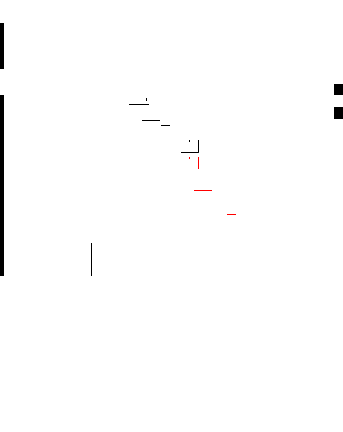
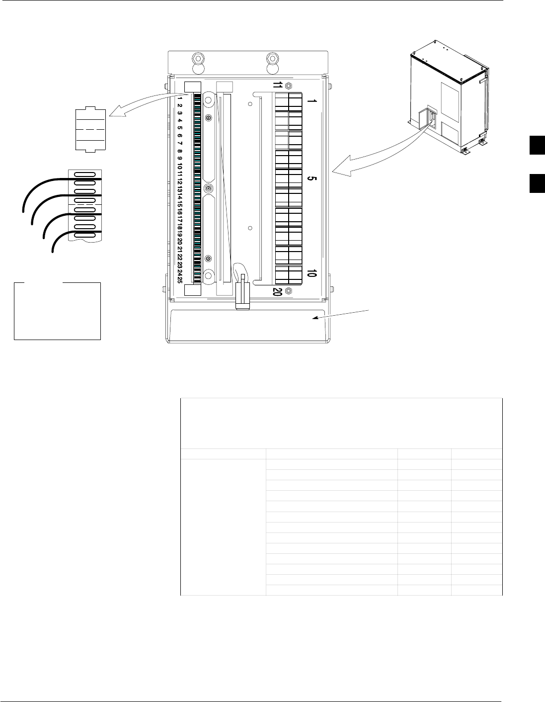
Folder Structure Overview
The LMF uses a <x>:\<lmf home directory> folder that contains all of
the essential data for installing and maintaining the BTS. The following
list outlines the folder structure for LMF. Except for the bts-nnn folders,
these folders are created as part of the LMF installation. Refer to the
CDMA LMF Operator’s Guide for a complete description of the folder
structure.
Figure 3-1: LMF Folder Structure
version folder (A separate folder is
required for each different version; for
example, a folder name 2.8.1.1.1.5.)
loads folder
(C:)
x:\<lmf home directory> folder
cdma folder
code folder
data folder
BTS-nnn folders (A separate folder is
required for each BTS where bts-nnn is the
unique BTS number; for example, bts-163.)
NOTE The “loads” folder and all the folders below it are not available
from the LMF for Software Release 2.16.1.x. These folders may
be present as as a legacy from previous software versions or
downloaded from the CBSC/OMC-R.
3
Span Lines - Interface and Isolation 68P09255A69-3
Aug 2002
1X SCt4812ET Lite BTS Optimization/ATP Software Release 2.16.1.x
PRELIMINARY
3-12
Span Lines - Interface and Isolation
T1/E1 Span Interface
NOTE At active sites, the OMC-R/CBSC must disable the BTS and
place it out of service (OOS). DO NOT remove the span line
cable connectors until the OMC-R/CBSC has disabled the BTS.
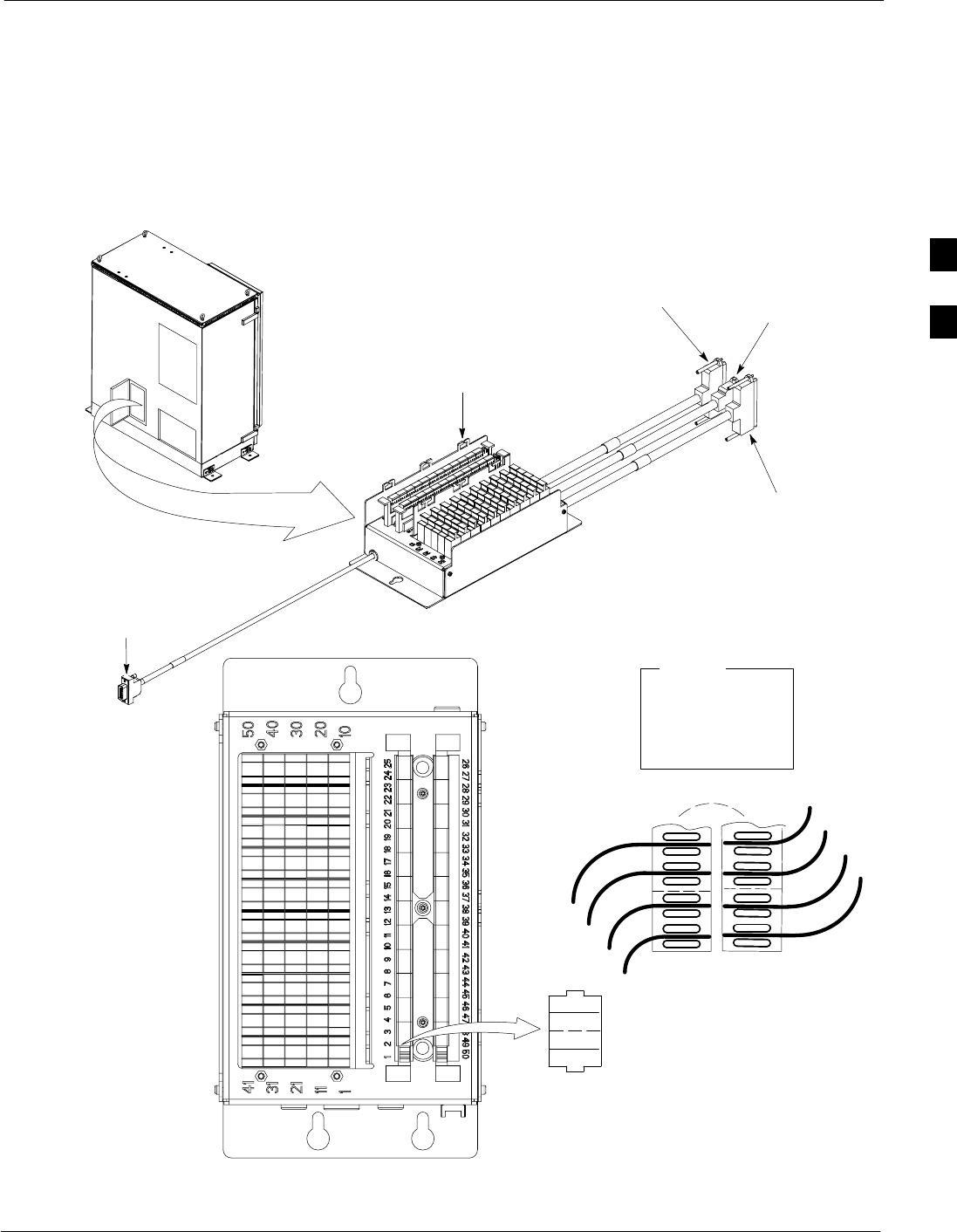
Each frame is equipped with one 50-pair punchblock for spans,
customer alarms, remote GPS, and BTS frame alarms. See Figure 3-4
and refer to Table 3-6 for the physical location and punchdown location
information.
Before connecting the LMF computer to the frame LAN, the
OMC-R/CBSC must disable the BTS and place it OOS. This will allow
the LMF to control the BTS, and prevent the CBSC from inadvertently
sending control information to the BTS during LMF-based tests.
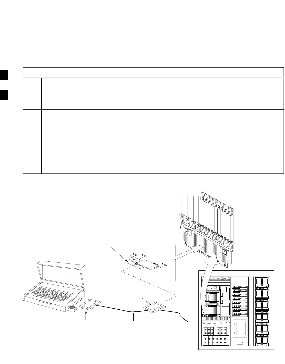
Isolate BTS from T1/E1 Spans
Once the OMC-R/CBSC has disabled the BTS, the spans must be
disabled to ensure the LMF will maintain control of the BTS. To disable
the spans, disconnect the BTS-to-CBSC Transcoder span cable
connectors from the Span I/O cards (Figure 3-2).
Figure 3-2: Disconnecting Span Lines
Span Line Cable
Connectors
4812ETL0020-1
3

Span Lines - Interface and Isolation68P09255A69-3
Aug 2002 1X SCt4812ET Lite BTS Optimization/ATP Software Release 2.16.1.x
PRELIMINARY
3-13
T1/E1 Span Isolation
Table 3-5 describes the action required for span isolation.
Table 3-5: T1/E1 Span Isolation
Step Action
1Have the OMCR/CBSC place the BTS OOS.
2To disable the span lines, locate the connector for the span or spans which must be disabled and
remove the respective connector from the applicable SCCP cage Span I/O board (Figure 3-2).
Configure Optional Channel Service Units
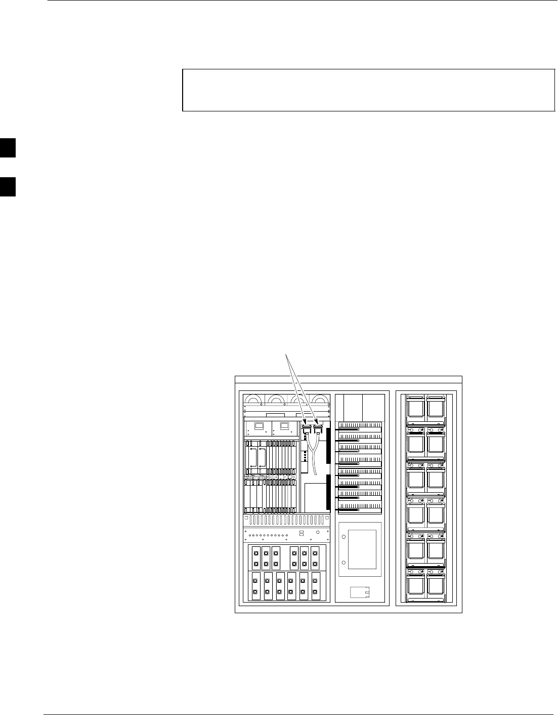
The M-PATH 537 Channel Service Unit (CSU) module provides
in-band SNMP-managed digital service access to T1 and fractional T1
lines. The M-PATH 437 Channel Service Unit (CSU) module provides
in-band SNMP-managed digital service access to E1 and fractional E1
lines. CSU modules plug into the CSU shelf (see Figure 3-3).
The CSU shelf can support two M-PATH 537 or two M-PATH 437 CSU
modules. A 537 CSU module supports a single T1 span connection. A
437 CSU module supports a single E1 span connection.
Remote M-PATH management is available through SNMP over an
in-band data link on the span line (using a facility data link or
8-64 Kbps of a DS0 channel). The unit at the near end of the
management path can be an SNMP manager or another M-PATH CSU.
Programming of the M-PATH is accomplished through the DCE 9-pin
connector on the front panel of the CSU shelf. Manuals and an MS
Windows programming disk are supplied with each unit.
For more information refer to M-PATH T1 Channel Service Unit User’s
Guide, Kentrox part number 65-77538101 or the ADC M-PATH E1
Channel Service Unit User’s Guide, Kentrox part number 1174139.
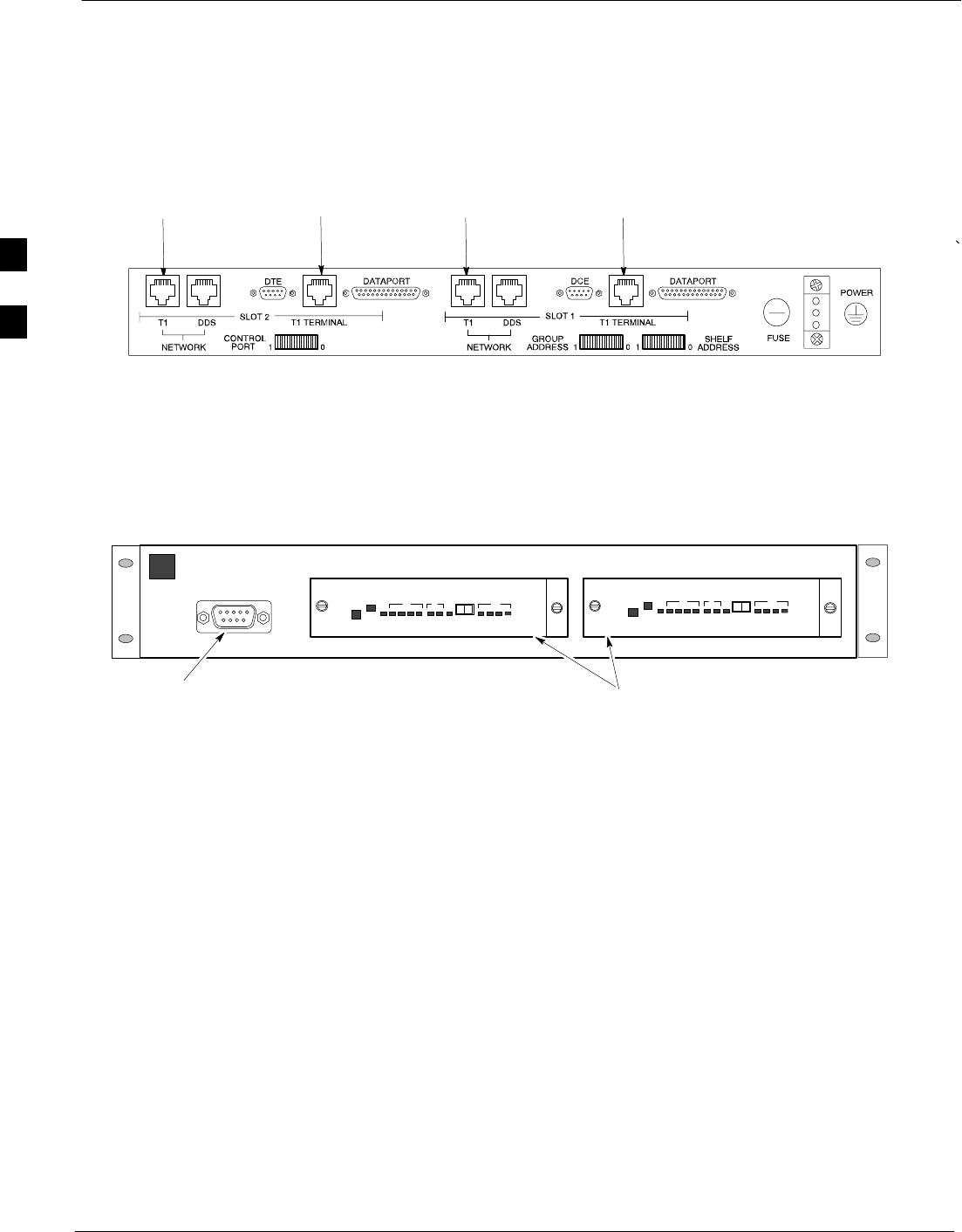
Setting the Control Port
Whichever control port is chosen, it must first be configured so the
control port switch settings match the communication parameters being
used by the control device. If using the rear-panel DTE control port, set
the SHELF ADDRESS switch SA5 to “up.” If using the rear-panel DCE
control port, position the SHELF ADDRESS switch down.
For more information, refer to the 2-Slot Universal Shelf Installation
Guide, Kentrox part number 65-78070001, the M-PATH T1 Channel
Service Unit Installation Guide, Kentrox part number 65-77538001, or
the M-PATH E1 Channel Service Unit Installation Guide, Kentrox part
number 1174662, depending on installed equipment.
Plug one of the cables listed below into the Control Port connectors:
Part Number Description of Cable
01-95006-022 (six feet) DB-9S to DB-9P
01-95010-022 (ten feet)
The control port cables can be used to connect the shelf to:
3
Span Lines - Interface and Isolation 68P09255A69-3
Aug 2002
1X SCt4812ET Lite BTS Optimization/ATP Software Release 2.16.1.x
PRELIMINARY
3-14
SA PC using the AT 9-pin interface
SA modem using the 9-pin connector
SOther shelves in a daisy chain
Figure 3-3: Rear and Front View of CSU Shelf
Front View
SLOT 1 SLOT 2
DCE Connector
(Craft Port)
Rear View
To/From
Network To/From
GLI To/From
Network To/From
GLI
CSU Modules
4812ETL0029-1
3
Span Lines - Interface and Isolation68P09255A69-3
Aug 2002 1X SCt4812ET Lite BTS Optimization/ATP Software Release 2.16.1.x
PRELIMINARY
3-15
Alarm, Span Line, and RGPS Cable Pin/Signal Information
See Figure 3-4 and refer to Table 3-6 for the physical location and
punchdown location information for the 50-pair punchblock.
Figure 3-4: 50-Pair Punchblock
TOP VIEW OF PUNCHBLOCK
STRAIN RELIEVE INCOMING
CABLE TO BRACKET WITH
TIE WRAPS
2T
1T
1R
2T
2R
1
2
1R
2R
LEGEND
1T = PAIR 1 - TIP
1R = PAIR 1 -RING
” ”
” ”
” ”
Frame Power Entry
Compartment
50R
50T
49R
49T
1T
TO SPAN I/O
CONNECTOR
TO ALARM
CONNECTOR TO MODEM
CONNECTOR
TO RGD/RGPS
CONNECTOR
SC4812ETL0010-1
3

Span Lines - Interface and Isolation 68P09255A69-3
Aug 2002
1X SCt4812ET Lite BTS Optimization/ATP Software Release 2.16.1.x
PRELIMINARY
3-16
Table 3-6: Punchdown Location for Stand-alone and Companion Frame
50-Pair Punch Block
Site Component Signal Name Punchdown Color
1T
1R
2T
2R
3T
3R
NOT 4T
USED 4R
5T
5R
6T
6R
7T
LFR_HSO_GND 7R Orange
EXT_IPPS_POS 8T Red
EXT_IPPS_NEG 8R White
LFR/HSO CAL_+ 9T Red
CAL_- 9R Green
LORAN_ + 10T Red
LORAN_ - 10R Blue
Pilot Beacon Alarm - Minor 11T
Pilot Beacon Alarm - Rtn 11R
Pilot Beacon Alarm - Major 12T
PILOT BEACON Pilot Beacon Control - NO 12R
Pilot Beacon Control-COM 13T
Pilot Beacon Control - NC 13R
Customer Outputs 1 - NO 14T
Customer Outputs 1 - COM 14R
Customer Outputs 1 - NC 15T
Customer Outputs 2 - NO 15R
Customer Outputs 2 - COM 16T
Customer Outputs 2 - NC 16R
Customer Outputs 3 - NO 17T
Customer Outputs 3 - COM 17R
Customer Outputs 3 - NC 18T
Customer Outputs 4 - NO 18R
Customer Outputs 4-COM 19T
Customer Outputs 4 - NC 19R
Customer Inputs 1 20T
Cust_Rtn_A_1 20R
Customer Inputs 2 21T
CUSTOMER Cust_Rtn_A_2 21R
CUSTOMER
OUTPUTS / INPUTS Customer Inputs 3 22T
Cust_Rtn_A_3 22R
Customer Inputs 4 23T
Cust_Rtn_A_4 23R
Customer Inputs 5 24T
Cust_Rtn_A_5 24R
Customer Inputs 6 25T
Cust_Rtn_A_6 25R
Customer Inputs 7 26T
Cust_Rtn_A_7 26R
Customer Inputs 8 27T
Cust_Rtn_A_8 27R
Customer Inputs 9 28T
Cust_Rtn_A_9 28R
Customer Inputs 10 29T
Cust_Rtn_A_10 29R
. . . continued on next page
3

Span Lines - Interface and Isolation68P09255A69-3
Aug 2002 1X SCt4812ET Lite BTS Optimization/ATP Software Release 2.16.1.x
PRELIMINARY
3-17
Table 3-6: Punchdown Location for Stand-alone and Companion Frame
50-Pair Punch Block
Site Component ColorPunchdownSignal Name
RCV_TIP_A 30T Red/Bk
RCV_RING_A 30R Red
XMIT_TIP_A 31T White/Bk
XMIT_RING_A 31R White
RCV_TIP_B 32T Green/Bk
RCV_RING_B 32R Green
XMIT_TIP_B 33T Blue/Bk
XMIT_RING_B 33R Blue
RCV_TIP_C 34T Yellow/Bk
RCV_RING_C 34R Yellow
XMIT_TIP_C 35T Brown/Bk
XMIT_RING_C 35R Brown
SPAN RCV_TIP_D 36T Orange/Bk
RCV_RING_D 36R Orange
XMIT_TIP_D 37T Violet/Bk
XMIT_RING_D 37R Violet
RCV_TIP_E 38T Gray/Bk
RCV_RING_E 38R Gray
XMIT_TIP_E 39T Pink/Bk
XMIT_RING_E 39R Pink
RCV_TIP_F 40T Tan/Bk
RCV_RING_F 40R Tan
XMIT_TIP_F 41T Bk/White
XMIT_RING_F 41R Bk
42T
42R
43T
For Frames without 43R
RGD Expansion (20-pair)
Punchblock See Table 3-7 44T
Punchblock See Table 3-7 44R
RGPS 45T
For Frames with RGD Expansion 45R
(20-pair) Punchblock 46T
See Table 3-8 46R
47T
47R
Telco_Modem_T 48T
Phone Line Telco_Modem_R 48R
Chassis Ground 49T Cable Drain
Reserved 49R
Miscellaneous Reserved 50T
Reserved 50R
. . . continued on next page
Table 3-7: 50-Pair Punch Block RGPS Punchdown Location for
RGPS Non-Expansion Frames (Input from RGPS Receiver)
and
Secondary RGPS Expansion Frames
(Input from RGPS Expansion Primary Frame 20-pair Punchblock)
Site Component Signal Name Punchdown Color
. . . continued on next page
3

Span Lines - Interface and Isolation 68P09255A69-3
Aug 2002
1X SCt4812ET Lite BTS Optimization/ATP Software Release 2.16.1.x
PRELIMINARY
3-18
Table 3-7: 50-Pair Punch Block RGPS Punchdown Location for
RGPS Non-Expansion Frames (Input from RGPS Receiver)
and
Secondary RGPS Expansion Frames
(Input from RGPS Expansion Primary Frame 20-pair Punchblock)
Site Component ColorPunchdownSignal Name
GPS_POWER_A+ 42T Yellow
GPS_POWER_A- 42R Yellow/Bk
GPS_POWER_B+ 43T Blue
GPS_POWER_B- 43R Blue/Bk
RGPS GPS_TX+ 44T White
For frames without GPS_TX- 44R White/Bk
RGD Expansion GPS_RX+ 45T Green
(20-pair)
Punchblock GPS_RX- 45R Green/Bk
Punchblock Signal Ground 46T Red
Master Frame 46R Red/Bk
GPS_1pps+ 47T Brown
GPS_1pps- 47R Brown/Bk
Table 3-8: 50-Pair Punch Block RGPS Punchdown Location for
RGPS Expansion Primary Frame
(Input from RGPS Receiver)
Site Component Signal Name Punchdown Color
GPS_POWER_A+ 42T Yellow
GPS_POWER_A- 42R Yellow/Bk
GPS_POWER_B+ 43T Blue
GPS_POWER_B- 43R Blue/Bk
RGPS GPS_TX+ 44T Green
For frames with GPS_TX- 44R Green/Bk
RGD Expansion GPS_RX+ 45T White
(20-pair)
Punchblock GPS_RX- 45R White/Bk
Punchblock Signal Ground 46T Red
Master Frame 46R Red/Bk
GPS_1pps+ 47T Brown
GPS_1pps- 47R Brown/Bk
Remote GPS Distribution Punchdown Information
See Figure 3-5 and refer to Table 3-9 for the physical location and RGPS
distribution 20-pair punchblock punchdown information for the RGPS
distribution cabling to the the RGPS expansion secondary frame.
3
Span Lines - Interface and Isolation68P09255A69-3
Aug 2002 1X SCt4812ET Lite BTS Optimization/ATP Software Release 2.16.1.x
PRELIMINARY
3-19
Figure 3-5: 20-pair Punchblock with RGD Module Punchdowns
Rear of RGPS Expansion
Primary Frame
(Power Entry Compartment
Door Open)
20-pair Punchblock with RGD Module
(Rotated 30_ Left) ETL0032-1
RGD
(All interconnect
cabling not shown for
clarity.)
1T
1R
2T
2R
2T
1R
2R
1T
LEGEND
1T = PAIR 1 - TIP
1R = PAIR 1 -RING
” ”
” ”
” ”
Table 3-9: 20-Pair Punch Block RGPS EXP(ansion) 1 Punchdown Location
for
RGPS Expansion Output to Secondary Frame
(Input from RGPS Receiver Through Primary Frame 50-pair Punchblock)
Site Component Signal Name Punchdown Color
GPS_POWER_A+ 1T Yellow
GPS_POWER_A- 1R Yellow/Bk
GPS_POWER_B+ 2T Blue
GPS_POWER_B- 2R Blue/Bk
GPS_RX+ 3T Green
GPS_RX- 3R Green/Bk
RGPS GPS_TX+ 4T White
RGPS GPS_TX- 4R White/Bk
Signal Ground 5T Red
Master Frame 5R Red/Bk
GPS_1pps+ 6T Brown
GPS_1pps- 6R Brown/Bk
Chassis Ground 19T Cable Drain
3
LMF to BTS Connection 68P09255A69-3
Aug 2002
1X SCt4812ET Lite BTS Optimization/ATP Software Release 2.16.1.x
PRELIMINARY
3-20
LMF to BTS Connection
Connect the LMF to the BTS
The LMF computer may be connected to the LAN A or B connector
located behind the frame lower air intake grill. Figure 3-6 below shows
the general location of these connectors. LAN A is considered the
primary LAN.
Table 3-10: Connecting the LMF to the BTS
Step Action
1To gain access to the LAN connectors, open the LAN cable and utility shelf access panel, then pull
apart the hook-and-loop fabric covering the BNC “T” connector (see Figure 3-6). If desired, slide
out the utility shelf for the LMF computer.
2Connect the LMF computer to the LAN A (left-hand) BNC connector via PCMCIA Ethernet Adapter.
NOTE
Xircom Model PE3-10B2 or equivalent can also be used to interface the LMF Ethernet connection to
the BTS frame connected to the PC parallel port, powered by an external AC/DC transformer. In this
case, the BNC cable must not exceed three feet in length.
* IMPORTANT
The LAN shield is isolated from chassis ground. The LAN shield (exposed portion of BNC connector)
must not touch the chassis during optimization.
Figure 3-6: LMF Connection Detail
LMF BNC “T” CONNECTIONS
ON LEFT SIDE OF FRAME
(ETHERNET “A” SHOWN;
ETHERNET “B” COVERED
WITH HOOK-AND-LOOP
FABRIC)
LMF COMPUTER
TERMINAL WITH
MOUSE PCMCIA ETHERNET
ADPATER & ETHERNET
UTP ADAPTER
UNIVERSAL TWISTED
PAIR (UTP) CABLE (RJ11
CONNECTORS)
10BASET/10BASE2
CONVERTER CONNECTS
DIRECTLY TO BNC T
115 VAC POWER
CONNECTION
NOTE:
Open LAN CABLE ACCESS
door. Pull apart hook-and-loop
fabric and gain access to the
LAN A or LAN B LMF BNC
connector.
SC4812ETL0012-2
3

Using the LMF68P09255A69-3
Aug 2002 1X SCt4812ET Lite BTS Optimization/ATP Software Release 2.16.1.x
PRELIMINARY
3-21
Using the LMF
Basic LMF Operation
LMF Coverage in This Publication - The LMF application program
supports maintenance of both CDMA and SAS BTSs. All references to
the LMF in this publication are to the CDMA portion of the program.
Operating Environments - The LMF application program allows the
user to work in the two following operating environments which are
accessed using the specified desktop icons:
SGraphical User Interface (GUI) using the WinLMF icon
SCommand Line Interface (CLI) using the WinLMF CDMA CLI icon
The GUI is the primary optimization and acceptance testing operating
environment. The CLI environment provides additional capability to the
user to perform manually controlled acceptance tests and audit the
results of optimization and calibration actions.
Basic Operation - Basic operation of the LMF in either environment
includes performing the following:
SSelecting and deselecting BTS devices
SEnabling devices
SDisabling devices
SResetting devices
SObtaining device status
The following additional basic operation can be performed in a GUI
environment:
SSorting a status report window
For detailed information on performing these and other LMF operations,
refer to the LMF Help function on-line documentation.
NOTE Unless otherwise noted, LMF procedures in this manual are
performed using the GUI environment.
The LMF Display and the BTS
BTS Display - When the LMF is logged into a BTS, a frame tab is
displayed for each RF modem frame (RFMF). For SC4812-series BTSs,
the BTS frames are considered the RFMFs. The frame tab will be
labeled with “CDMA” and the BTS number, a dash, and the frame
number (for example, BTS-812-1 for BTS 812, RFMF 1). If, as with a
single-frame SC4812ET Lite, there is only one frame for the BTS, there
will only be one tab.
CDF Requirements - For the LMF to recognize the devices installed in
the BTS, a BTS CDF file which includes equipage information for all
the devices in the BTS must be located in the applicable <x>:\<lmf
home directory>\cdma\bts-# folder. To provide the necessary channel
assignment data for BTS operation, a CBSC CDF file which includes
channel data for all BTS RFMFs is also required in the folder.
3
Using the LMF 68P09255A69-3
Aug 2002
1X SCt4812ET Lite BTS Optimization/ATP Software Release 2.16.1.x
PRELIMINARY
3-22
RFDS Display - If an RFDS is included in the CDF file, an RFDS tab
labeled with “RFDS,” a dash and the BTS number-frame number
combination (for example, RFDS-812-1 ) will be displayed.
Logging Into a BTS
Logging into a BTS establishes a communication link between the BTS
and the LMF. An LMF session can be logged into only one BTS at a
time.
Prerequisites
Before attempting to log into a BTS, ensure the following have been
completed:
SThe LMF is correctly installed on the LMF computer.
SA bts-nnn folder with the correct CDF and CBSC files exists.
SThe LMF computer was connected to the BTS before starting the
Windows operating system and the LMF software. If necessary, restart
the computer after connecting it to the BTS in accordance with
Table 3-10 and Figure 3-6.
CAUTION Be sure that the correct bts-#.cdf and cbsc-#.cdf file is used for
the BTS. These should be the CDF files that are provided for the
BTS by the CBSC. Failure to use the correct CDF files can
result in invalid optimization. Failure to use the correct CDF
files to log into a live (traffic-carrying) site can shut down
the site.
BTS Login from the GUI Environment
Follow the procedures in Table 3-11 to log into a BTS when using the
GUI environment.
Table 3-11: BTS GUI Login Procedure
nStep Action
1Start the LMF GUI environment by double-clicking on the WinLMF desktop icon (if the LMF is
not running).
- An LMF window will open and display the LMF build number in the title bar.
NOTE
If a warning similar to the following is displayed, select No, shut down other LMF sessions which
may be running, and start the LMF GUI environment again:
The CLI handler is already running.
This may cause conflicts with the LMF.
Are you sure you want to start the application?
Yes No
2Click on Login tab (if not displayed).
. . . continued on next page
3

Using the LMF68P09255A69-3
Aug 2002 1X SCt4812ET Lite BTS Optimization/ATP Software Release 2.16.1.x
PRELIMINARY
3-23
Table 3-11: BTS GUI Login Procedure
nActionStep
3Double click on CDMA (in the Available Base Stations pick list).
4Click on the desired BTS number.
5Click on the Network Login tab (if not already in the forefront).
6Enter correct IP address (normally 128.0.0.2) for a field BTS, if not correctly displayed in the IP
Address box.
7Type in the correct IP Port number (normally 9216) if not correctly displayed in the IP Port box.
8Click on Ping.
- If the connection is successful, the Ping Display window shows text similar to the following:
Reply from 128 128.0.0.2: bytes=32 time=3ms TTL=255
- If there is no response the following is displayed:
128.0.0.2:9216:Timed out
If the MGLI fails to respond, reset and perform the ping process again. If the MGLI still fails to
respond, typical problems are shorted BNC to inter-frame cabling, open cables, crossed A and B
link cables, missing 50-Ohm terminators, or the MGLI itself.
9Select the Multi-channel Preselector type from the Multi-channel Preselector drop-down list
(default is MPC) to a device corresponding to your BTS configuration, if required.
NOTE
Use a Tower Top Amplifier is not applicable to the SC4812ET Lite.
10 Click on Login. (A BTS tab with the BTS and frame numbers is displayed.)
NOTE
SIf an attempt is made to log into a BTS that is already logged on, all devices will be gray.
SThere may be instances where the BTS initiates a log out due to a system error (i.e., a device
failure).
SIf the MGLI is OOS-ROM (blue), it must be downloaded with RAM code before other devices
can be seen.
SIf the MGLI is OOS-RAM (yellow), it must be enabled before other installed devices can be
seen.
3

Using the LMF 68P09255A69-3
Aug 2002
1X SCt4812ET Lite BTS Optimization/ATP Software Release 2.16.1.x
PRELIMINARY
3-24
BTS Login from the CLI Environment
Follow the procedures in Table 3-12 to log into a BTS when using the
CLI environment.
NOTE If the CLI and GUI environments are to be used at the same
time, the GUI must be started first and BTS login must be
performed from the GUI. Refer to Table 3-11 to start the GUI
environment and log into a BTS.
Table 3-12: BTS CLI Login Procedure
nStep Action
1Double-click the WinLMF CLI desktop icon (if the LMF CLI environment is not already
running).
2NOTE
If a BTS was logged into under a GUI session before the CLI environment was started, the CLI
session will be logged into the same BTS, and step 2 is not required.
At the /wlmf prompt, enter the following command:
login bts-<bts#> host=<host> port=<port>
where:
host = MGLI card IP address (defaults to address last logged into for this BTS or 128.0.0.2 if this
is first login to this BTS)
port = IP port of the BTS (defaults to port last logged into for this BTS or 9216 if this is first login
to this BTS)
A response similar to the following will be displayed:
LMF>
13:08:18.882 Command Received and Accepted
COMMAND=login bts-33
13:08:18.882 Command In Progress
13:08:21.275 Command Successfully Completed
REASON_CODE=”No Reason”
3
Using the LMF68P09255A69-3
Aug 2002 1X SCt4812ET Lite BTS Optimization/ATP Software Release 2.16.1.x
PRELIMINARY
3-25
Logging Out
Logging out of a BTS is accomplished differently for the GUI and CLI
operating environments.
NOTE The GUI and CLI environments use the same connection to a
BTS. If a BTS is logged into in both the GUI and CLI
environments at the same time, logging out of the BTS in either
environment will log out of it for both. When either a login or
logout is performed in the CLI window, there is no GUI
indication that the login or logout has occurred.
Logging Out of a BTS from the GUI Environment
Follow the procedure in Table 3-13 to logout of a BTS when using the
GUI environment.
Table 3-13: BTS GUI Logout Procedure
nStep Action
1Click on BTS in the BTS menu bar.
2Click the Logout item in the pull-down menu (a Confirm Logout pop-up message will appear).
3Click on Yes (or press the Enter key) to confirm logout. The Login tab will appear.
NOTE
If a logout was previously performed on the BTS from a CLI window running at the same time as
the GUI, a Logout Error pop-up message will appear stating the system could not log out of the
BTS. When this occurs, the GUI must be exited and restarted before it can be used for further
operations.
4If a Logout Error pop-up message appears stating that the system could not log out of the Base
Station because the given BTS is not logged in, click OK and proceed to step 5.
5 Select File > Exit in the window menu bar, click Yes in the Confirm Logout pop-up, and click
OK in the Logout Error pop-up which appears again.
6If further work is to be done in the GUI, restart it.
NOTE
SThe Logout item on the BTS menu bar will only log you out of the displayed BTS.
SYou can also log out of all BTS sessions and exit LMF by clicking on the File selection in the
menu bar and selecting Exit from the File menu list. A Confirm Logout pop-up message will
appear.
3

Using the LMF 68P09255A69-3
Aug 2002
1X SCt4812ET Lite BTS Optimization/ATP Software Release 2.16.1.x
PRELIMINARY
3-26
Logging Out of a BTS from the CLI Environment
Follow the procedure in Table 3-14 to logout of a BTS when using the
CLI environment.
Table 3-14: BTS CLI Logout Procedure
nStep Action
NOTE
If the BTS is also logged into from a GUI running at the same time and further work must be done
with it in the GUI, proceed to step 2.
1Log out of a BTS by entering the following command:
logout bts-<bts#>
A response similar to the following will be displayed:
LMF>
13:24:51.028 Command Received and Accepted
COMMAND=logout bts-33
13:24:51.028 Command In Progress
13:24:52.04 Command Successfully Completed
REASON_CODE=”No Reason”
2If desired, close the CLI interface by entering the following command:
exit
A response similar to the following will be displayed before the window closes:
Killing background processes....
Establishing an MMI Communication Session
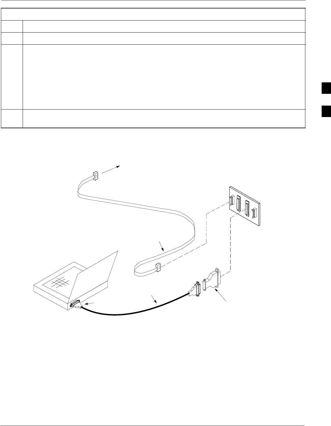
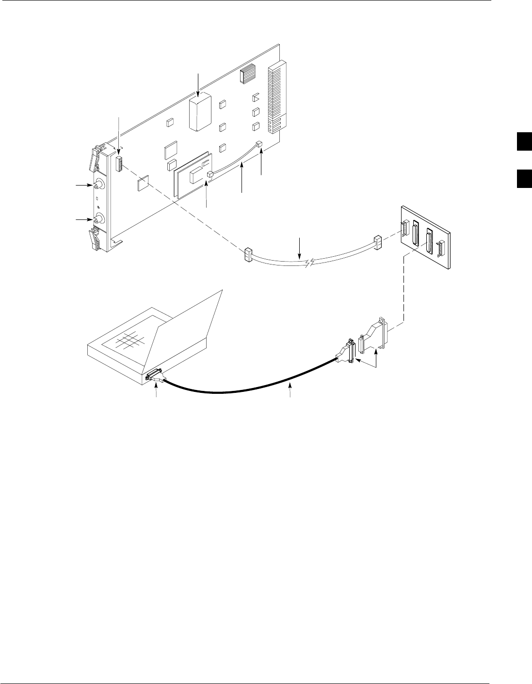
Equipment Connection - Figure 3-7 illustrates common equipment
connections for the LMF computer. For specific connection locations on
FRUs, refer to the illustration accompanying the procedures which
require the MMI communication session.
Initiate MMI Communication - For those procedures which require
MMI communication between the LMF and BTS FRUs, follow the
procedures in Table 3-15 to initiate the communication session.
Table 3-15: Establishing MMI Communication
Step Action
1Connect the LMF computer to the equipment as detailed in the applicable procedure which requires
the MMI communication session.
2If the LMF computer has only one serial port (COM1) and the LMF is running, disconnect the LMF
from COM1 by performing the following:
2a - Click on Tools in the LMF window menu bar, and select Options from the pull-down menu list.
-- An LMF Options dialog box will appear.
. . . continued on next page
3
Using the LMF68P09255A69-3
Aug 2002 1X SCt4812ET Lite BTS Optimization/ATP Software Release 2.16.1.x
PRELIMINARY
3-27
Table 3-15: Establishing MMI Communication
Step Action
2b - In the LMF Options dialog box, click the Disconnect Port button on the Serial Connection tab.
3Start the named HyperTerminal connection for MMI sessions by double clicking on its Windows
desktop shortcut.
NOTE
If a Windows desktop shortcut was not created for the MMI connection, access the connection from the
Windows Start menu by selecting:
Programs > Accessories > Hyperterminal > HyperTerminal > <Named HyperTerminal
Connection (e.g., MMI Session)>
4Once the connection window opens, establish MMI communication with the BTS FRU by pressing
the LMF computer Enter key until the prompt identified in the applicable procedure is obtained.
Figure 3-7: LMF Computer Common MMI Connections
NULL MODEM
BOARD
(TRN9666A)
8-PIN TO 10-PIN
RS-232 CABLE (P/N
30-09786R01)
RS-232 CABLE
8-PIN
LMF
COMPUTER
To FRU MMI port
DB9-TO-DB25
ADAPTER
COM1
OR
COM2
Online Help
Task oriented online help is available in the LMF by clicking on Help in
the window menu bar, and selecting LMF Help from the pull-down
menu.
3
Pinging the Processors 68P09255A69-3
Aug 2002
1X SCt4812ET Lite BTS Optimization/ATP Software Release 2.16.1.x
PRELIMINARY
3-28
Pinging the Processors
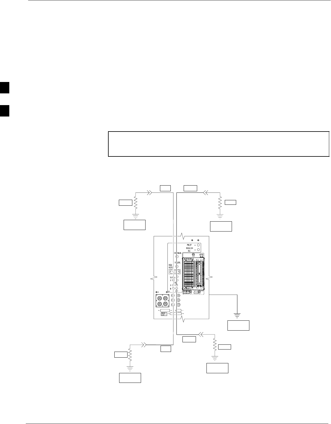
Pinging the BTS
For proper operation, the integrity of the Ethernet LAN A and B links
must be verified. Figure 3-8 represents a typical BTS Ethernet
configuration for an SC4812ET Lite stand-alone or companion frame.
The drawing depicts cabling and termination for both the A and B
LANs.
Ping is a program that sends request data packets to hosts on a network,
in this case GLI modules on the BTS LAN, to obtain a response from the
“target” host specified by an IP address.
Follow the steps in Table 3-16 to ping each processor (on both LAN A
and LAN B) and verify LAN redundancy is working properly.
CAUTION Always wear an approved anti-static wrist strap while handling
any circuit card/module to prevent damage by Electro-Static
Discharge (ESD).
Figure 3-8: BTS Ethernet LAN Termination Diagram
SIGNAL
GROUND
SIGNAL
GROUND
50Ω
IN
SC4812ET Lite
SIGNAL
GROUND
50Ω
50Ω
SIGNAL
GROUND
50Ω
SIGNAL
GROUND
FRAME GROUND
TRIAX
TERMINATOR
TRIAX
TERMINATOR
TRIAX
TERMINATOR
IN
OUT
OUT
SC4812ETL0013-5
TRIAX
TERMINATOR
3

Pinging the Processors68P09255A69-3
Aug 2002 1X SCt4812ET Lite BTS Optimization/ATP Software Release 2.16.1.x
PRELIMINARY
3-29
NOTE The Ethernet LAN A and B cables and/or terminations must be
installed on each frame/enclosure external LAN connector before
performing this test. All other processor board LAN connections
are made through the backplanes.
Table 3-16: Pinging the Processors
Step Action
1If this is a first-time communication with a newly-installed frame or a GLI card which has been
replaced, perform the procedure in Table 6-3 and then return to step 2.
2Be sure any uncabled LAN A and B IN and OUT connectors in the power entry compartment (rear of
frame - Figure 3-4 and Figure 3-8) are terminated with 50 Ω loads.
3If it has not already been done, connect the LMF computer to the BTS (refer to Table 3-10 and
Figure 3-6.)
4If it has not already been done, start a GUI LMF session and log into the BTS ( refer to Table 3-11).
5In the power entry compartment, remove the 50Ω termination on the frame LAN B IN connector.
- The LMF session should remain active.
6Replace the 50Ω terminator on the BTS frame LAN B IN connector.
7From the Windows desktop, click the Start button and select Run.
8In the Open box, type ping and the MGLI IP address (for example, ping 128.0.0.2).
NOTE
128.0.0.2 is the default IP address for the GLI card in slot GLI-1 in field BTS units.
9Click on OK.
10 If the targeted module responds, a DOS window will appear with a display similar to the following:
Reply from 128.0.0.2: bytes=32 time=3ms TTL=255
- If the device responds, proceed to step 18.
If there is no response, the following is displayed:
Request timed out
- If the GLI fails to respond, it should be reset and re-pinged. If it still fails to respond, typical
problems would be: failure of the LMF to login, shorted BNC-to-inter-frame cabling, open
cables, crossed A and B link cables, or the GLI itself.
11 Logout of the BTS as described in Table 3-13, exit from the LMF program, and restart the Windows
operating system on the LMF computer.
12 Restart the LMF GUI program as described in LMF Help function on-line documentation, and log into
the BTS as described in Table 3-11.
13 Perform steps 7 through 10 again.
- If the device responds, proceed to step 18.
If there is still no response, proceed to step 14.
. . . continued on next page
3

Pinging the Processors 68P09255A69-3
Aug 2002
1X SCt4812ET Lite BTS Optimization/ATP Software Release 2.16.1.x
PRELIMINARY
3-30
Table 3-16: Pinging the Processors
Step Action
14 If ping was unsuccessful after restarting the LMF computer, press the MGLI front panel reset
pushbutton and perform steps 7 through 10 again.
NOTE
Refer to Table 6-1 if ping was unsuccessful after resetting the MGLI.
15 After the BTS has been successfully pinged, be sure the 50Ω termination was replaced on the BTS
frame LAN B IN connector in the power entry compartment (Figure 3-8). Disconnect the LMF cable
from the LAN shelf LAN A connector, and connect it to LAN B (right-hand connector) (refer to
Figure 3-6).
16 In the power entry compartment, remove the 50Ω termination on the BTS frame LAN A IN connector.
17 Repeat steps 5 through 9 using LAN B.
18 After the BTS has been successfully pinged on the secondary LAN, replace the 50Ω termination on
the frame LAN A IN connector in the power entry compartment.
19 Disconnect the LMF cable from the LAN shelf LAN B and connect it to LAN A.
20 Remove and replace the 50Ω termination on the LAN B IN connector to force the MGLI to switch to
primary LAN A.
21 Repeat steps 5 through 9 to ensure proper primary LAN operation.
3

Download the BTS68P09255A69-3
Aug 2002 1X SCt4812ET Lite BTS Optimization/ATP Software Release 2.16.1.x
PRELIMINARY
3-31
Download the BTS
Overview
Before a BTS can operate, each equipped device must contain device
initialization (ROM) code. ROM code is loaded in all devices during
manufacture, factory repair, or, for software upgrades, from the CBSC
using the DownLoad Manager (DLM). Device application (RAM) code
and data must be downloaded to each equipped device by the user before
the BTS can be made fully functional for the site where it is installed.
ROM Code
Downloading ROM code to BTS devices from the LMF is NOT routine
maintenance or a normal part of the optimization process. It is only
done in unusual situations where the resident ROM code release level in
the device is not compatible with the required release level of the site
operating software and the CBSC can not communicate with the BTS to
perform the download. An example would be a BTS loaded with R16.0
software where a GLI which is factory-loaded with R9.2.x or earlier
ROM code must be installed to replace a malfunctioning GLI.
Before ROM code can be downloaded from the LMF, the correct ROM
code file for each device to be loaded must exist on the LMF computer.
ROM code must be manually selected for download.
NOTE The ROM code file is not available for GLI3s. GLI3s are ROM
code loaded at the factory.
ROM code can be downloaded to a device that is in any state. After the
download is started, the device being downloaded will change to
OOS_ROM (blue). The device will remain OOS_ROM (blue) when the
download is completed. A compatible revision-level RAM code must
then be downloaded to the device. Compatible code loads for ROM and
RAM must be used for the device type to ensure proper performance.
The compatible device code release levels for the BSS software release
being used are listed in the Version Matrix section of the SCt CDMA
Release Notes (supplied on the tape or CD-ROM containing the BSS
software).
Procedures to load ROM code are located in Appendix G.
RAM Code
Before RAM code can be downloaded from the LMF, the correct RAM
code file for each device must exist on the LMF computer. RAM code
can be automatically or manually selected depending on the Device
menu item chosen and where the RAM code file for the device is stored
in the LMF file structure. The RAM code file will be selected
automatically if the file is in the <x>:\<lmf home
directory>\cdma\loads\n.n.n.n\code folder (where n.n.n.n is the
download code version number that matches the “NextLoad” parameter
of the CDF file). The RAM code file in the code folder must have the
correct hardware bin number for the device to be loaded.
RAM code can be downloaded to a device that is in any state. After the
download is started, the device being loaded will change to OOS_ROM
(blue). When the download is completed successfully, the device will
change to OOS_RAM (yellow).
3
Download the BTS 68P09255A69-3
Aug 2002
1X SCt4812ET Lite BTS Optimization/ATP Software Release 2.16.1.x
PRELIMINARY
3-32
When code is downloaded to an MGLI or GLI, the LMF automatically
also downloads data and then enables the MGLI. When enabled, the
MGLI will change to INS_ACT (bright green). A redundant GLI will
not be automatically enabled and will remain OOS_RAM (yellow).
When the redundant GLI is manually commanded to enable through the
LMF, it will change state to INS_SBY (olive green).
For non-GLI devices, data must be downloaded after RAM code is
downloaded. To download data, the device state must be OOS_RAM
(yellow).
The devices to be loaded with RAM code and data are:
SMaster Group Line Interface (MGLI)
SRedundant GLI
SClock Synchronization Module (CSM) (Only if new revision code
must be loaded)
SMulti Channel CDMA (MCC24E, MCC8E, or MCC-1X) cards
SBroadband Transceiver (BBX2 or BBX-1X) cards
SRFDS Test Subscriber Interface Card (TSIC) or RFDS-1X RFDS
PROCessor (RPROC) card, if RFDS is installed
NOTE The MGLI must be successfully downloaded with RAM code
and data, and in INS_ACT (bright green) status before
downloading any other device. The RAM code download
process for an MGLI automatically downloads data and then
enables the MGLI.
Verify GLI ROM Code Loads
Devices should not be loaded with a RAM code version which is not
compatible with the ROM code with which they are loaded. Before
downloading RAM code and data to the processor cards, follow the
procedure in Table 3-17 to verify the GLI devices are loaded with the
correct ROM code for the software release used by the BSS.
Prerequisite
Identify the correct GLI ROM code load for the software release being
used on the BSS by referring to the Version Matrix section of the SCt
CDMA Release Notes (supplied on the tapes or CD-ROMs containing
the BSS software).
Table 3-17: Verify GLI ROM Code Loads
Step Action
1If it has not already been done, start a GUI LMF session and log into the BTS ( refer to Table 3-11).
2Select all GLI devices by clicking on them, and select Device > Status from the BTS menu bar.
3In the status report window which opens, note the number in the ROM Ver column for each GLI2.
4If the ROM code loaded in the GLIs is not the correct one for the software release being used on the
BSS, perform the following:
. . . continued on next page
3

Download the BTS68P09255A69-3
Aug 2002 1X SCt4812ET Lite BTS Optimization/ATP Software Release 2.16.1.x
PRELIMINARY
3-33
Table 3-17: Verify GLI ROM Code Loads
Step Action
4a - Log out of the BTS as described in Table 3-13 or Table 3-14, as applicable.
4b - Disconnect the LMF computer.
4c - Reconnect the span lines as described in Table 5-7.
4d - Have the CBSC download the correct ROM code version to the BTS devices.
5When the GLIs have the correct ROM load for the software release being used, be sure the span lines
are disabled as outlined in Table 3-5 and proceed to downloading RAM code and data.
Download RAM Code and Data to MGLI and GLI
Follow the steps outlined in Table 3-18 to download the RAM code and
data to the MGLI and other installed GLI devices.
Prerequisites
SPrior to performing these procedures, ensure a code file exists for each
of the devices to be loaded (refer to Table 3-3).
SThe LMF computer is connected to the BTS (refer to Table 3-10), and
is logged in using the GUI environment (refer to Table 3-11).
Table 3-18: Download and Enable MGLI and GLI Devices
Step Action
1Be sure the LMF will use the correct software release for code and data downloads by performing the
following steps:
1a - Click on Tools in the LMF menu bar, and select Update NextLoad > CDMA from the pull-down
menus.
1b - Click on the BTS to be loaded.
-- The BTS will be highlighted.
1c - Click the button next to the correct code version for the software release being used.
-- A black dot will appear in the button circle.
1d - Click Save.
1e - Click OK to close each of the advisory boxes which appear.
2Prepare to download code to the MGLI by clicking on the device.
3 Click Device in the BTS menu bar, and select Download > Code/Data in the pull-down menus.
- A status report is displayed confirming change in the device(s) status.
4 Click OK to close the status window.
- The MGLI will automatically be downloaded with data and enabled.
5Once the MGLI is enabled, load and enable additional installed GLIs by clicking on the devices and
repeating steps 3 and 4.
6 Click OK to close the status window for the additional GLI devices.
3
Download the BTS 68P09255A69-3
Aug 2002
1X SCt4812ET Lite BTS Optimization/ATP Software Release 2.16.1.x
PRELIMINARY
3-34
Download RAM Code and Data to Non-GLI Devices
Downloads to non-GLI devices can be performed individually for each
device or all installed devices can be downloaded with one action.
NOTE - CSM devices are RAM code-loaded at the factory. RAM
code is downloaded to CSMs only if a newer software
version needs to be loaded.
- When downloading to multiple devices, the download may
fail for some of the devices (a time-out occurs). These
devices can be loaded individually after completing the
multiple download.
Follow the steps in Table 3-19 to download RAM code and data to
non-GLI devices.
Table 3-19: Download RAM Code and Data to Non-GLI Devices
Step Action
1Select the target CSM, MCC, and/or BBX device(s) by clicking on them.
2 Click Device in the BTS menu bar, and select Download > Code/Data in the pull-down menus.
- A status report is displayed that shows the results of the download for each selected device.
3Click OK to close the status report window when downloading is completed.
NOTE
After a BBX, CSM, or MCC device is successfully loaded with RAM code and data have changed to
the OOS_RAM state (yellow), the status LED should be rapidly flashing GREEN.
BBX Cards Remain OOS_ROM
If BBX cards remain OOS_ROM (blue) after power-up or following
code load, refer to Table 6-7, steps 8 and 9.
Selecting CSM Clock Source and Enabling CSMs
CSMs must be enabled prior to enabling the MCCs. Procedures in the
following two sub-sections cover the actions to accomplish this. For
additional information on the CSM sub-system, see “Clock
Synchronization Manager (CSM) Sub-system Description” in the CSM
System Time - GPS & LFR/HSO Verification section of this chapter.
Select CSM Clock Source - A CSM can have three different clock
sources. The Select CSM Source function can be used to select the clock
source for each of the three inputs. This function is only used if the clock
source for a CSM needs to be changed. The Clock Source function
provides the following clock source options:
SLocal GPS
SMate GPS
SRemote GPS
SHSO (only for source 2 & 3)
SHSO Extender
3
Download the BTS68P09255A69-3
Aug 2002 1X SCt4812ET Lite BTS Optimization/ATP Software Release 2.16.1.x
PRELIMINARY
3-35
SLFR (only for source 2 & 3)
S10 MHz (only for source 2 & 3)
SNONE (only for source 2 & 3)
Prerequisites
SMGLI is INS_ACT (bright green)
SCSM is OOS_RAM (yellow) or INS_ACT (bright green)
Table 3-20: Select CSM Clock Source
Step Action
1Display the CSM cage view in the LMF by clicking on the CSM area of the SCCP shelf in the picture
of the BTS frame.
2When the CSM cage view replaces the GLI/MCC/BBX view, click on the CSM(s) for which the clock
source is to be selected.
3Click on Device in the BTS menu bar, and select CSM/MAWI > Select Clock Source... in the
pull-down menu list.
- A CSM clock reference source selection window will appear.
4Select the applicable clock source in the Clock Reference Source pick lists. Uncheck the related
check boxes for Clock Reference Sources 2 and 3 if you do not want the displayed pick list item to be
used.
5Click on the OK button.
- A status report is displayed showing the results of the operation.
6Click on the OK button to close the status report window.
NOTE For RF-GPS, verify the CSM configured with the GPS receiver
“daughter board” is installed in the SCCP shelf CSM 1 slot
before continuing.
Enable CSMs - Follow the steps outlined in Table 3-21 to enable the
CSMs installed in the SCCP shelves.
Table 3-21: Enable CSMs
Step Action
1NOTE
If equipped with two CSMs, enable card in slot CSM 2 first.
Click on the target CSM.
2Click on Device in the BTS menu bar, and select Enable in the pull-down menu list.
- A status report is displayed showing the results of the enable operation.
. . . continued on next page
3

Download the BTS 68P09255A69-3
Aug 2002
1X SCt4812ET Lite BTS Optimization/ATP Software Release 2.16.1.x
PRELIMINARY
3-36
Table 3-21: Enable CSMs
Step Action
3 Click OK to close the status report window.
NOTE
SThe board in slot CSM 1 interfaces with the GPS receiver (either on-board or remote). The enable
sequence for this board can take up to one hour (see below).
SFAIL may be shown in the status report table for a slot CSM 1 enable action. If Waiting For Phase
Lock is shown in the Description field, do not cancel the enable process. The CSM will change to
the Enabled state after phase lock is achieved.
NOTE
The GPS satellite system satellites are not in a geosynchronous orbit and are maintained and operated
by the United States Department of Defense (DOD). The DOD periodically alters satellite orbits;
therefore, satellite trajectories are subject to change. A GPS receiver that is INS contains an ephemeris
(satellite position table) that is updated periodically to take these changes into account.
If a GPS receiver has not been updated for a number of weeks, it may take up to an hour for the GPS
receiver ephemeris to be updated.
Once updated, the GPS receiver must track at least four satellites and obtain (hold) a 3-D position fix
for a minimum of 45 seconds before the CSM will come in service. (In some cases, the GPS receiver
needs to track only one satellite, depending on accuracy mode set during the data load).
NOTE
SIf two CSMs are installed and the board in slot CSM 1 has enabled, the LMF CSM cage view
should show slot CSM 1 as bright green (INS-ACT) and slot CSM 2 as olive green (INS-SBY)
SIf more than an hour has passed without the board in slot CSM 1 enabling, refer to the CSM System
Time - GPS & LFR/HSO Verification section of this chapter (see Table 3-23, Figure 3-9, and
Table 3-24) to determine the cause.
4After CSMs have been successfully enabled, be sure the PWR/ALM LEDs are steady green
(alternating green/red indicates the card is in an alarm state).
3
Download the BTS68P09255A69-3
Aug 2002 1X SCt4812ET Lite BTS Optimization/ATP Software Release 2.16.1.x
PRELIMINARY
3-37
Enable MCCs
This procedure configures the MCC and sets the “tx fine adjust”
parameter. The “tx fine adjust” parameter is not a transmit gain setting,
but a timing adjustment that compensates for the processing delay in the
BTS (approximately 3 mS).
Follow the steps outlined in Table 3-22 to enable the MCCs installed in
the SCCP shelves.
NOTE The MGLI and CSM must be downloaded and enabled, prior to
downloading and enabling an MCC.
Table 3-22: Enable MCCs
Step Action
1If the GLI/MCC/BBX view is not displayed in the LMF window, click on the GLI/MCC/BBX area of the
SCCP shelf.
2Click on the target MCC(s), or click on Select in the BTS menu bar, and select MCCs in the
pull-down menu list.
3click on Device in the BTS menu bar, and select Enable in the pull-down menu list.
- A status report is displayed showing the results of the enable operation.
4 Click OK to close the status report window.
3

CSM System Time - GPS & LFR/HSO Verification 68P09255A69-3
Aug 2002
1X SCt4812ET Lite BTS Optimization/ATP Software Release 2.16.1.x
PRELIMINARY
3-38
CSM System Time - GPS & LFR/HSO Verification
Clock Synchronization Manager (CSM) Sub-system Description
Overview - Each BTS CSM sub-system features two CSM boards per
RFMF. The primary function of the CSM cards is to maintain CDMA
system time. GPS is used as the primary timing reference and
synchronizes the entire cellular system. In typical operation, the primary
CSM locks its Digital Phase Locked Loop (DPLL) circuits to GPS
signals. These signals are provided by either an on-board GPS receiver
module (RF-GPS) or a remote GPS receiver (RGPS). RGPS uses a GPS
receiver in the antenna head that has a digital output. The second
generation CSM card (CSM-II) is required when using the RGPS. A
CSM-II card can also be equipped with a local GPS receiver daughter
card to support an RF-GPS signal.
SCCP Shelf CSM Card Slot Assignments - The GPS receiver is
interfaced to the board in SCCP shelf slot CSM 1. This card is the
primary timing source, while the card in slot CSM 2 provides
redundancy. The redundant card, does not have a GPS receiver.
CSM-II Card Type Description - Each CSM-II card features a
temperature-stabilized crystal oscillator that provides 19.6608 MHz
clock, even second pulse, and 3 MHz reference signals to the
synchronization source selected from the following (refer to Table 3-24
for source selection/verification procedures):
SGPS: local/RF-GPS or remote/RGPS
SLORAN-C Low Frequency Receiver (LFR) or High Stability
Oscillator (HSO)
SExternal reference oscillator sources
CDMA Clock Distribution Card (CCD) Description - CCD cards
buffer and distribute even-second reference and 19.6608 MHz clock
signals from the CSM cards. CCD 1 is married to the card in slot CSM
1, and CCD 2 is married to the card in slot CSM 2.
CSM Card Redundancy - The BTS switches between the primary and
redundant units (card slots CSM 1 and CSM 2, respectively) upon failure
or command. A failure in CSM 1 or CCD 1 will cause the system to
switch to the CSM 2-CCD 2 redundant card pair. GPS timing
synchronization is continually maintained between the primary and
redundant CSM-CCD pairs.
Secondary Timing References - The BTS may be equipped with a
LORAN-C Low Frequency Receiver (LFR), a High Stability Oscillator
(HSO), or external 10 MHz Rubidium source which the CSM can use as
a secondary timing reference. Continuous GPS synchronization is
maintained for the LFR or HSO secondary timing references. The CSM
monitors and determines what reference to use at a given time.
3

CSM System Time - GPS & LFR/HSO Verification68P09255A69-3
Aug 2002 1X SCt4812ET Lite BTS Optimization/ATP Software Release 2.16.1.x
PRELIMINARY
3-39
Timing Source Fault Management - Fault management has the
capability of switching between the GPS synchronization source and the
LFR/HSO backup source in the event of a GPS receiver failure. During
normal operation, the card in slot CSM 1 selects GPS as the primary
timing source (Table 3-24). The source selection can also be overridden
via the LMF or by the system software.
Low Frequency Receiver/
High Stability Oscillator
General
The CSM and the LFR/HSO - The CSM performs the overall
configuration and status monitoring functions for the LFR/HSO. In the
event of GPS failure, the LFR/HSO is capable of maintaining
synchronization initially established by the GPS reference signal.
LFR - The LFR requires an active external antenna to receive
LORAN-C RF signals. Timing pulses are derived from this signal,
which is synchronized to Universal Time Coordinates (UTC) and GPS
time. The LFR can maintain system time indefinitely after initial GPS
lock.
HSO - The HSO is a high stability 10 MHz oscillator with the necessary
interface to the CSMs. The HSO is typically installed in those
geographical areas not covered by the LORAN-C system. Since the
HSO is a free-standing oscillator, system time can only be maintained
for 24 hours after 24 hours of GPS lock
Upgrades and Expansions: LFR2/HSO2/HSOX
The LFR2 and HSO2 (second generation cards) both can export a timing
signal to other BTS frames located at a site. These secondary frames
require an HSO-expansion (HSOX) module whether the primary frame
has an LFR2 or an HSO2. The HSOX accepts input from the primary
frame and interfaces with the CSM cards in the secondary frames. LFR
and LFR2 use the same source code in source selection (Table 3-24).
HSO, HSO2, and HSOX use the same source code in source selection
(Table 3-24).
NOTE Allow the base site and test equipment to warm up for 60
minutes after any interruption in oscillator power. CSM card
warm-up allows the oscillator oven temperature and oscillator
frequency to stabilize prior to test. Test equipment warm-up
allows the Rubidium standard time base to stabilize in frequency
before any measurements are made.
3
CSM System Time - GPS & LFR/HSO Verification 68P09255A69-3
Aug 2002
1X SCt4812ET Lite BTS Optimization/ATP Software Release 2.16.1.x
PRELIMINARY
3-40
CSM Frequency Verification
The objective of this procedure is the initial verification of the Clock
Synchronization Module (CSM) cards before performing the RF path
verification tests.
Test Equipment Setup
(GPS & LFR/HSO Verification)
Follow the steps outlined in Table 3-23 to set up test equipment.
Table 3-23: Test Equipment Setup (GPS & LFR/HSO Verification)
Step Action
1Perform one of the following as required by installed equipment:
1a - For local GPS (RF-GPS): Verify a CSM card with a GPS receiver is installed in the primary
CSM slot, CSM 1, and that the card is INS_ACT (bright green).
NOTE
Verify by checking the card ejectors for kit number SGLN1145 on the card in slot CSM 1.
1b - For Remote GPS (RGPS): Verify a CSM-II card is installed in primary slot CSM 1 and that the
card is INS_ACT (bright green).
NOTE
Verify by checking the card ejectors for kit number SGLN4132ED or subsequent.
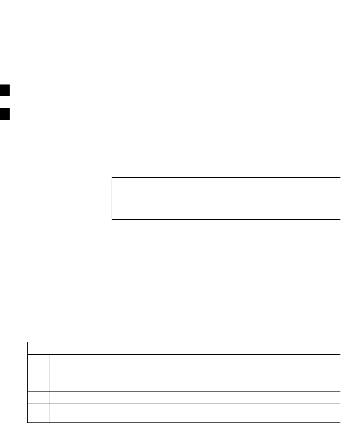
2Remove the card from slot CSM 2 (if installed) and connect a serial cable from the LMF COM 1 port
(via null modem card) to the MMI port on the card in slot CSM 1 (see Figure 3-9).
3Reinstall the card removed from slot CSM 2.
4Start an MMI communication session with the card in slot CSM 1 by using the Windows desktop
shortcut icon (see Table 3-15) .
5When the terminal screen appears press the Enter key until the CSM> prompt appears.
CAUTION In the power entry compartment, connect the GPS antenna to the
RF GPS connector ONLY. Damage to the GPS antenna and/or
receiver can result if the GPS antenna is inadvertently connected
to any other RF connector.
3
CSM System Time - GPS & LFR/HSO Verification68P09255A69-3
Aug 2002 1X SCt4812ET Lite BTS Optimization/ATP Software Release 2.16.1.x
PRELIMINARY
3-41
Figure 3-9: CSM MMI Terminal Connection
NULL MODEM
BOARD
(TRN9666A)
RS-232 SERIAL
MODEM CABLE
DB9-TO-DB25
ADAPTER
COM1
LMF
NOTEBOOK
FW00372
CSM card shown
removed from frame
19.6 MHZ TEST
POINT REFERENCE
(NOTE 1)
EVEN SECOND
TICK TEST POINT
REFERENCE
GPS RECEIVER
ANTENNA INPUT
GPS RECEIVER
MMI SERIAL
PORT
ANTENNA COAX
CABLE
REFERENCE
OSCILLATOR
9-PIN TO 9-PIN
RS-232 CABLE
NOTES:
1. One LED on each CSM:
Green = IN-SERVICE ACTIVE
Fast Flashing Green = OOS-RAM
Red = Fault Condition
Flashing Green & Red = Fault
GPS Initialization/Verification
Prerequisites
Ensure the following prerequisites have been met before proceeding:
SThe primary CSM and HSO (if equipped) has been warmed up for at
least 15 minutes.
SThe LMF computer is connected to the MMI port of the primary CSM
as shown in Figure 3-9.
SAn MMI communication session has been started (Table 3-15), and
the CSM> prompt is present in the HyperTerminal window
(Table 3-23).
Follow the steps outlined in Table 3-24 to initialize and verify proper
GPS receiver functioning.
3

CSM System Time - GPS & LFR/HSO Verification 68P09255A69-3
Aug 2002
1X SCt4812ET Lite BTS Optimization/ATP Software Release 2.16.1.x
PRELIMINARY
3-42
Table 3-24: GPS Initialization/Verification
Step Action
1To verify that Clock alarms (0000), Dpll is locked and has a reference source, and
GPS self test passed messages are displayed within the report, issue the following MMI
command
bstatus
- The system will display a response similar to the following:
Clock Alarms (0000):
DPLL is locked and has a reference source.
GPS receiver self test result: passed
Time since reset 0:33:11, time since power on: 0:33:11
2Enter the following command at the CSM> prompt to display the current status of the Loran and GPS
receivers:
sources
- When equipped with LFR, the system will generate a response similar to the following:
N Source Name Type TO Good Status Last Phase Target Phase Valid
-------------------------------------------------------------------------
0LocalGPS Primary 4 YES Good 00Yes
1 LFR CHA Secondary 4 YES Good -2013177 -2013177 Yes
2 Not Used
Current reference source number: 0
- When equipped with HSO, the system will generate a response similar to the following:
Num Source Name Type TO Good Status Last Phase Target Phase Valid
----------------------------------------------------------------------------
0 Local GPS Primary 4 Yes Good 3 0 Yes
1HSO Backup 4 No N/A timed-out* Timed-out* No
*NOTE “Timed-out” should only be displayed while the HSO is warming up. “Not-Present” or
“Faulty” should not be displayed. If the HSO does not appear as one of the sources, then configure the
HSO as a back-up source by entering the following command at the CSM> prompt:
ss 1 12
After a maximum of 15 minutes, the Rubidium oscillator should reach operational temperature and the
LED on the HSO should now have changed from red to green. After the HSO front panel LED has
changed to green, enter sources <cr> at the CSM> prompt. Verify that the HSO is now a valid source
by confirming that the bold text below matches the response of the “sources” command.
The HSO should be valid within one (1) minute, assuming the DPLL is locked and the HSO rubidium
oscillator is fully warmed.
Num Source Name Type TO Good Status Last Phase Target Phase Valid
----------------------------------------------------------------------------
0 Local GPS Primary 4 Yes Good 3 0 Yes
1HSO Backup 4 Yes N/A xxxxxxxxxx xxxxxxxxxx Yes
. . . continued on next page
3
CSM System Time - GPS & LFR/HSO Verification68P09255A69-3
Aug 2002 1X SCt4812ET Lite BTS Optimization/ATP Software Release 2.16.1.x
PRELIMINARY
3-43
Table 3-24: GPS Initialization/Verification
Step Action
3HSO information (underlined text above, verified from left to right) is usually the #1 reference source.
If this is not the case, have the OMCR determine the correct BTS timing source has been identified in
the database by entering the display bts csmgen command and correct as required using the edit
csm csmgen refsrc command.
NOTE
If any of the above areas fail, verify:
- If LED is RED, verify that HSO had been powered up for at least 5 minutes. After oscillator
temperature is stable, LED should go GREEN Wait for this to occur before continuing !
- If “timed out” is displayed in the Last Phase column, suspect the HSO output buffer or oscillator
is defective
- Verify the HSO is FULLY SEATED and LOCKED to prevent any possible card warpage
4Verify the following GPS information (underlined text above):
- GPS information is usually the 0 reference source.
- At least one Primary source must indicate “Status = good” and “Valid = yes” to bring site up.
. . . continued on next page
3

CSM System Time - GPS & LFR/HSO Verification 68P09255A69-3
Aug 2002
1X SCt4812ET Lite BTS Optimization/ATP Software Release 2.16.1.x
PRELIMINARY
3-44
Table 3-24: GPS Initialization/Verification
Step Action
5Enter the following command at the CSM> prompt to verify that the GPS receiver is in tracking mode.
gstatus
- Observe the following typical response:
24:06:08 GPS Receiver Control Task State: tracking satellites.
24:06:08 Time since last valid fix: 0 seconds.
24:06:08
24:06:08 Recent Change Data:
24:06:08 Antenna cable delay 0 ns.
24:06:08 Initial position: lat 117650000 msec, lon -350258000 msec, height 0 cm (GPS)
24:06:08 Initial position accuracy (0): estimated.
24:06:08
24:06:08 GPS Receiver Status:
24:06:08 Position hold: lat 118245548 msec, lon -350249750 msec, height 20270 cm
24:06:08 Current position: lat 118245548 msec, lon -350249750 msec, height 20270 cm
(GPS)
24:06:08 8 satellites tracked, receiving 8 satellites, 8 satellites visible.
24:06:08 Current Dilution of Precision (PDOP or HDOP): 0.
24:06:08 Date & Time: 1998:01:13:21:36:11
24:06:08 GPS Receiver Status Byte: 0x08
24:06:08 Chan:0, SVID: 16, Mode: 8, RSSI: 148, Status: 0xa8
24:06:08 Chan:1, SVID: 29, Mode: 8, RSSI: 132, Status: 0xa8
24:06:08 Chan:2, SVID: 18, Mode: 8, RSSI: 121, Status: 0xa8
24:06:08 Chan:3, SVID: 14, Mode: 8, RSSI: 110, Status: 0xa8
24:06:08 Chan:4, SVID: 25, Mode: 8, RSSI: 83, Status: 0xa8
24:06:08 Chan:5, SVID: 3, Mode: 8, RSSI: 49, Status: 0xa8
24:06:08 Chan:6, SVID: 19, Mode: 8, RSSI: 115, Status: 0xa8
24:06:08 Chan:7, SVID: 22, Mode: 8, RSSI: 122, Status: 0xa8
24:06:08
24:06:08 GPS Receiver Identification:
24:06:08 COPYRIGHT 1991-1996 MOTOROLA INC.
24:06:08 SFTW P/N # 98-P36830P
24:06:08 SOFTWARE VER # 8
24:06:08 SOFTWARE REV # 8
24:06:08 SOFTWARE DATE 6 AUG 1996
24:06:08 MODEL # B3121P1115
24:06:08 HDWR P/N # _
24:06:08 SERIAL # SSG0217769
24:06:08 MANUFACTUR DATE 6B07
24:06:08 OPTIONS LIST IB
24:06:08 The receiver has 8 channels and is equipped with TRAIM.
6Verify the following GPS information (shown above in underlined text):
- At least 4 satellites are tracked, and 4 satellites are visible.
- GPS Receiver Control Task State is “tracking satellites”. Do not continue until this occurs!
- Dilution of Precision indication is not more that 30.
Record the current position base site latitude, longitude, height and height reference (height reference
to Mean Sea Level (MSL) or GPS height (GPS). (GPS = 0 MSL = 1).
. . . continued on next page
3
CSM System Time - GPS & LFR/HSO Verification68P09255A69-3
Aug 2002 1X SCt4812ET Lite BTS Optimization/ATP Software Release 2.16.1.x
PRELIMINARY
3-45
Table 3-24: GPS Initialization/Verification
Step Action
7If steps 1 through 6 pass, the GPS is good.
NOTE
If any of the above mentioned areas fail, verify that:
- If Initial position accuracy is “estimated” (typical), at least 4 satellites must be tracked and
visible (1 satellite must be tracked and visible if actual lat, log, and height data for this site has
been entered into CDF file).
- If Initial position accuracy is “surveyed,” position data currently in the CDF file is assumed to be
accurate. GPS will not automatically survey and update its position.
- The GPS antenna is not obstructed or misaligned.
- GPS antenna connector center conductor measureS approximately +5 Vdc with respect to the
shield.
- There is no more than 4.5 dB of loss between the GPS antenna OSX connector and the BTS frame
GPS input.
- Any lightning protection installed between GPS antenna and BTS frame is installed correctly.
8Enter the following commands at the CSM> prompt to verify that the CSM is warmed up and that GPS
acquisition has taken place.
debug dpllp
Observe the following typical response if the CSM is not warmed up (15 minutes from application of
power) (If warmed-up proceed to step 9)
CSM>DPLL Task Wait. 884 seconds left.
DPLL Task Wait. 882 seconds left.
DPLL Task Wait. 880 seconds left. ...........etc.
NOTE
The warm command can be issued at the MMI port used to force the CSM into warm-up, but the
reference oscillator will be unstable.
9Observe the following typical response if the CSM is warmed up.
c:17486 off: -11, 3, 6 TK SRC:0 S0: 3 S1:-2013175,-2013175
c:17486 off: -11, 3, 6 TK SRC:0 S0: 3 S1:-2013175,-2013175
c:17470 off: -11, 1, 6 TK SRC:0 S0: 1 S1:-2013175,-2013175
c:17486 off: -11, 3, 6 TK SRC:0 S0: 3 S1:-2013175,-2013175
c:17470 off: -11, 1, 6 TK SRC:0 S0: 1 S1:-2013175,-2013175
c:17470 off: -11, 1, 6 TK SRC:0 S0: 1 S1:-2013175,-2013175
10 Verify the following GPS information (underlined text above, from left to right):
- Lower limit offset from tracked source variable is not less than -60 (equates to 3µs limit).
- Upper limit offset from tracked source variable is not more than +60 (equates to 3µs limit).
- TK SRC: 0 is selected, where SRC 0 = GPS.
11 Enter the following commands at the CSM> prompt to exit the debug mode display.
debug dpllp
3

CSM System Time - GPS & LFR/HSO Verification 68P09255A69-3
Aug 2002
1X SCt4812ET Lite BTS Optimization/ATP Software Release 2.16.1.x
PRELIMINARY
3-46
LORAN-C Initialization/Verification
Table 3-25: LORAN-C Initialization/Verification
Step Action Note
1At the CSM> prompt, enter lstatus <cr> to verify that the LFR is in tracking
mode. A typical response is:
CSM> lstatus <cr>
LFR St ti St t
LFR Station Status:
Clock coherence: 512 >
5930M 51/60 dB 0 S/N Flag:
5930X 52/64 dn -1 S/N Flag:
5990 47/55 dB -6 S/N Flag:
7980M 62/66 dB 10 S/N Fl
This must be greater
than 100 before LFR
becomes a valid source.
7980M 62/66 dB 10 S/N Flag:
7980W 65/69 dB 14 S/N Flag: . PLL Station . >
7980X 48/54 dB -4 S/N Flag:
7980Y 46/58 dB -8 S/N Flag:E
7980Z 60/67 dB 8 S/N Flag:
8290M 50/65 dB 0 S/N Flag
This shows the LFR is
locked to the selected
PLL station.
8290M 50/65 dB 0 S/N Flag:
8290W 73/79 dB 20 S/N Flag:
8290W 58/61 dB 6 S/N Flag:
8290W 58/61 dB 6 S/N Flag:
8970M 89/95 dB 29 S/N Flag:
8970W 62/66 dB 10 S/N Flag:
8970X 73/79 dB 22 S/N Flag:
8970X 73/79 dB 22 S/N Fl
ag:
8970Y 73/79 dB 19 S/N Flag:
8970Z 62/65 dB 10 S/N Flag:
9610M 62/65 dB 10 S/N Fl
g
9610M 62/65 dB 10 S/N Flag:
9610V 58/61 dB 8 S/N Flag:
9610W 47
/
49 dB -4 S
/
N Fla
g
:E
9610W 47/49 dB -4 S/N Flag:E
9610X 46/57 dB -5 S/N Flag:E
9610Y 48/54 dB -5 S/N Flag:E
9610Z 65/69 dB 12 S/N Flag
9610Z 65/69 dB 12 S/N Flag:
9940M 50/53 dB -1 S/N Flag:S
9940W 49/56 dB -4 S/N Flag:E
9940W 49/56 dB 4 S/N Flag:E
9940Y 46/50 dB-10 S/N Flag:E
9960M 73/79 dB 22 S/N Flag:
9960W 51/60 dB 0 S/N Flag:
9960W 51/60 dB 0 S/N Fl
ag:
9960X 51/63 dB -1 S/N Flag:
9960Y 59/67 dB 8 S/N Flag:
9960Z 89/96 dB 29 S/N Fl
9960Z 89/96 dB 29 S/N Flag:
LFR Task State: lfr locked to station 7980W
LFR Recent Change Data:
Search List: 5930 5990 7980 8290 8970 9940 9610 9960 >
PLL GRI: 7980W
LFR Master, reset not needed, not the reference source.
CSM>
This search list and PLL
data must match the
configuration for the
geographical location
of the cell site.
. . . continued on next page
3
CSM System Time - GPS & LFR/HSO Verification68P09255A69-3
Aug 2002 1X SCt4812ET Lite BTS Optimization/ATP Software Release 2.16.1.x
PRELIMINARY
3-47
Table 3-25: LORAN-C Initialization/Verification
Step NoteAction
2Verify the following LFR information (highlighted above in boldface type):
- Locate the “dot” that indicates the current phase locked station assignment (assigned by MM).
- Verify that the station call letters are as specified in site documentation as well as M X Y Z
assignment.
- Verify the S/N ratio of the phase locked station is greater than 8.
3At the CSM> prompt, enter sources <cr> to display the current status of the the LORAN receiver.
- Observe the following typical response.
Num Source Name Type TO Good Status Last Phase Target Phase Valid
----------------------------------------------------------------------------
0 Local GPS Primary 4 Yes Good -3 0 Yes
1 LFR ch A Secondary 4 Yes Good -2013177 -2013177 Yes
2 Not used
Current reference source number: 1
*NOTE “Timed-out” should only be displayed while the LFR is warming up. “Not-Present” or
“Faulty” should not be displayed. If the LFR does not appear as one of the sources, then configure the
LFR as a back-up source by entering the following command at the CSM> prompt:
ss 1 2
4LORAN LFR information (highlighted above in boldface type) is usually the #1 reference source
(verified from left to right).
* IMPORTANT
If any of the above mentioned areas fail, verify:
- The LFR antenna is not obstructed or misaligned.
- The antenna pre-amplifier power and calibration twisted pair connections are intact and < 91.4 m
(300 ft) in length.
- A dependable connection to suitable Earth Ground is in place.
- The search list and PLL station for cellsite location are correctly configured .
NOTE
LFR functionality should be verified using the “source” command (as shown in Step 3). Use the
underlined responses on the LFR row to validate correct LFR operation.
5Close the HyperTerminal window.
3

Test Equipment Set-up 68P09255A69-3
Aug 2002
1X SCt4812ET Lite BTS Optimization/ATP Software Release 2.16.1.x
PRELIMINARY
3-48
Test Equipment Set-up
Connecting Test Equipment to the BTS
The following types of test equipment are required to perform calibration
and ATP tests:
SLMF
SCommunications system analyzer model supported by the LMF
SPower meter model supported by the LMF (required when using the
HP 8921A/600 and Advantest R3465 analyzers)
SNon-radiating transmit line termination load
SDirectional coupler and in-line attenuator
SRF cables and adapters
Refer to Table 3-26 for an overview of connections for test equipment
currently supported by the LMF. In addition, see the following figures:
SFigure 3-13, Figure 3-14, and Figure 3-15 show the test set
connections for TX calibration
SFigure 3-16 through Figure 3-21 show the test set connections for
optimization/ATP tests
Test Equipment GPIB Address Settings
All test equipment is controlled by the LMF through an IEEE-488/GPIB
bus. To communicate on the bus, each piece of test equipment must have
a GPIB address set which the LMF will recognize. The standard address
settings used by the LMF for the various types of test equipment items
are as follows:
SSignal generator address: 1
SPower meter address: 13
SCommunications system analyzer: 18
Using the procedures included in the Setting GPIB Addresses section of
Appendix NO TAG, verify and, if necessary, change the GPIB address of
each piece of employed test equipment to match the applicable addresses
above.
3

Test Equipment Set-up68P09255A69-3
Aug 2002 1X SCt4812ET Lite BTS Optimization/ATP Software Release 2.16.1.x
PRELIMINARY
3-49
Supported Test Equipment
CAUTION To prevent damage to the test equipment, all transmit (TX) test
connections must be through a 30 dB directional coupler plus a
20 dB in-line attenuator for both the 800 MHz and 1.9 GHz
BTSs.
IS-95A/B Operation
Optimization and ATP testing for IS-95A/B sites or carriers may be
performed using the following test equipment:
SCyberTest
SAdvantest R3267 spectrum analyzer with R3562 signal generator
SAdvantest R3465 spectrum analyzer with R3561L signal generator
and HP-437B or Gigatronics Power Meter
SAgilent E4406A transmitter test set with E4432B signal generator
SAgilent 8935 series E6380A communications test set (formerly HP
8935)
SHewlett-Packard HP 8921 (with CDMA interface and, for 1.9 GHz,
PCS Interface) and HP-437B or Gigatronics Power Meter
SSpectrum Analyzer (HP8594E) - optional
SRubidium Standard Timebase - optional
CDMA2000 1X Operation
Optimization and ATP testing for CDMA2000 1X sites or carriers may
be performed using the following test equipment:
SAdvantest R3267 spectrum analyzer with R3562 signal generator
SAgilent E4406A transmitter test set with E4432B signal generator
SAgilent 8935 series E6380A communications test set (formerly HP
8935) with option 200 or R2K and with E4432B signal generator for
1X FER
Test Equipment Preparation
See Appendix F for specific steps to prepare each type of test set and
power meter to perform calibration and ATP .
3
Test Equipment Set-up 68P09255A69-3
Aug 2002
1X SCt4812ET Lite BTS Optimization/ATP Software Release 2.16.1.x
PRELIMINARY
3-50
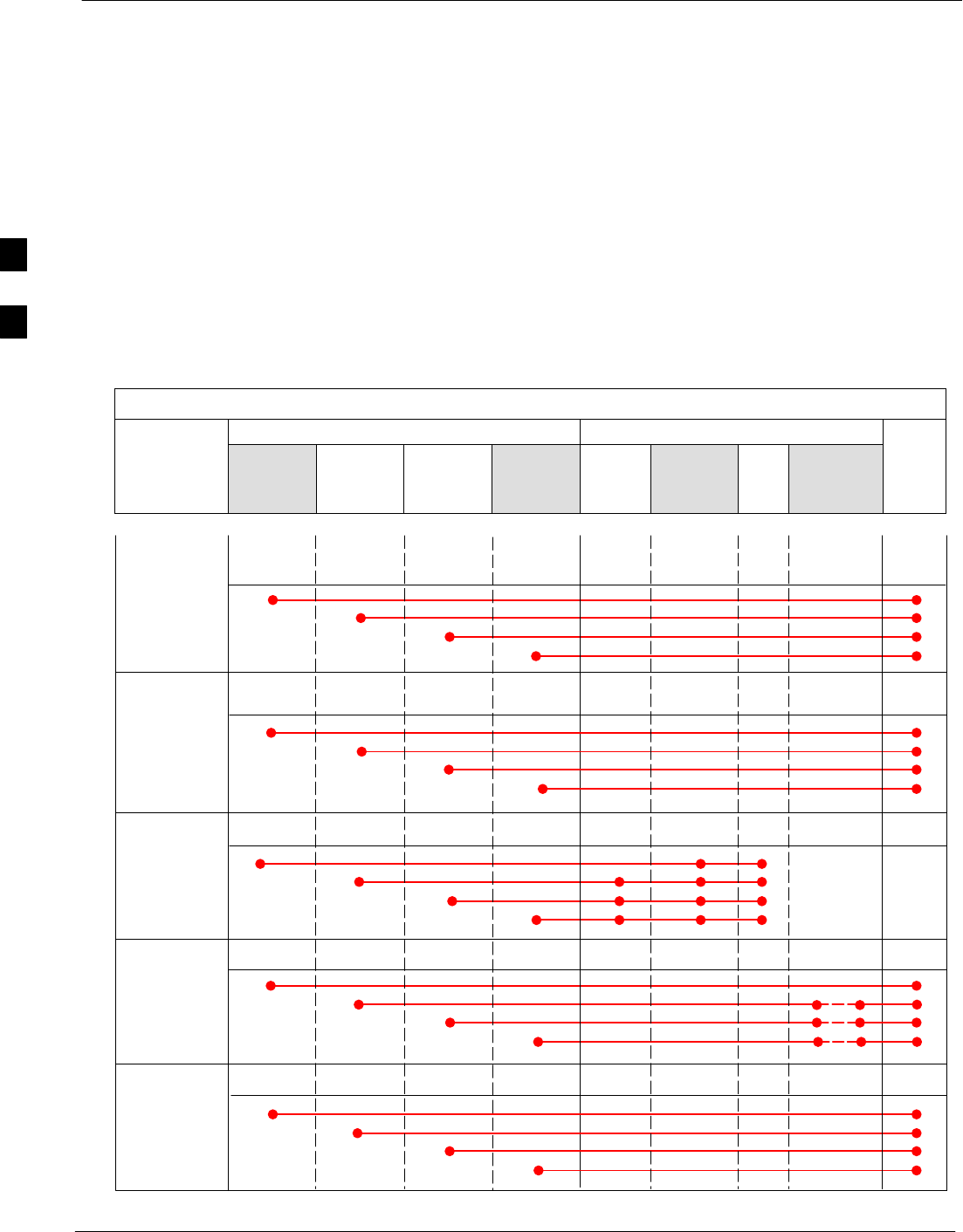
Test Equipment Connection Charts
To use the following charts to identify necessary test equipment
connections, locate the communications system analyzer being used in
the COMMUNICATIONS SYSTEM ANALYZER columns, and read down
the column. Where a dot appears in the column, connect one end of the
test cable to that connector. Follow the horizontal line to locate the end
connection(s), reading up the column to identify the appropriate
equipment and/or BTS connector.
IS-95A/B-only Test Equipment Connections
Table 3-26 depicts the interconnection requirements for currently
available test equipment supporting IS-95A/B only which meets
Motorola standards and is supported by the LMF.
Table 3-26: IS-95A/B-only Test Equipment Interconnection
COMMUNICATIONS SYSTEM ANALYZER ADDITIONAL TEST EQUIPMENT
SIGNAL Cyber-Test Advantest
R3465 HP 8921A HP 8921
W/PCS Power
Meter GPIB
Interface LMF
Attenuator
&
Directional
Coupler BTS
EVEN SECOND
SYNCHRONIZATION EVEN
SEC REF EVEN SEC
SYNC IN
EVEN
SECOND
SYNC IN
EVEN
SECOND
SYNC IN
19.6608 MHZ
CLOCK TIME
BASE IN
CDMA
TIME BASE
IN
CDMA
TIME BASE
IN
CDMA
TIME BASE
IN
CONTROL
IEEE 488 BUS IEEE
488 GPIB GPIB SERIAL
PORT
HP-IB HP-IB
TX TEST
CABLES RF
IN/OUT INPUT
50WTX1-6
RF
IN/OUT RF
IN/OUT 20 DB
ATTEN. BTS
PORT
RX TEST
CABLES RF
GEN OUT RF OUT
50WRX1-6
DUPLEX
OUT RF OUT
ONLY
SYNC
MONITOR
FREQ
MONITOR
HP-IB
3
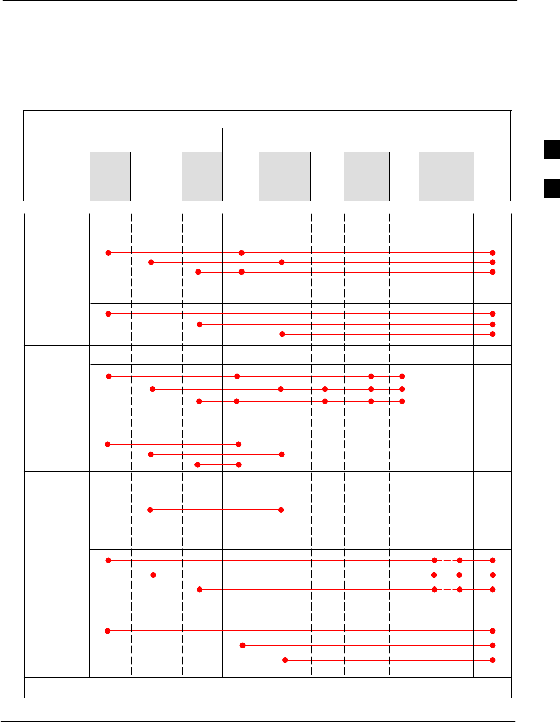
Test Equipment Set-up68P09255A69-3
Aug 2002 1X SCt4812ET Lite BTS Optimization/ATP Software Release 2.16.1.x
PRELIMINARY
3-51
CDMA2000 1X/IS-95A/B-capable Test Equipment
Connections
Table 3-27 depicts the interconnection requirements for currently
available test equipment supporting both CDMA 2000 1X and
IS-95A/B which meets Motorola standards and is supported by the
LMF.
Table 3-27: CDMA2000 1X/IS-95A/B Test Equipment Interconnection
COMMUNICATIONS SYSTEM
ANALYZER ADDITIONAL TEST EQUIPMENT
SIGNAL
Agilent
8935
(Option
200 or
R2K) Advantest
R3267 Agilent
E4406A
Agilent
E4432
Signal
Gen.
Advantest
R3562
Signal
Generator Power
Meter GPIB
Interface LMF
Attenuator
&
Directional
Coupler BTS
EVEN SECOND
SYNCHRONIZATION
EVEN
SECOND
SYNC IN EXT TRIG
IN
19.6608 MHZ
CLOCK EXT REF
IN MOD TIME
BASE IN
CONTROL
IEEE 488 BUS
10 MHZ
OUT
GP-IBHP-IB GP-IB GPIB SERIAL
PORT
GPIB GPIB
TX TEST
CABLES RF
IN/OUT INPUT
50 WTX1-6
20 DB
ATTEN. BTS
PORT
SYNC
MONITOR
FREQ
MONITOR
HP-IB
PATTERN
TRIG IN
EXT REF
IN
RF INPUT
50 W
RX TEST
CABLES RF OUT
50 W
RF OUTPUT
50 WRX1-6
10 MHZ 10 MHZ OUT
(SWITCHED) SYNTHE
REF IN
10 MHZ
IN
TRIGGER
IN
EXT TRIG
SIGNAL SOURCE
CONTROLLED
SERIAL I/O
SERIAL
I/O SERIAL
I/O
10 MHZ
REF OUT
* WHEN USED ALONE, THE AGILENT 8935 WITH OPTION 200 OR R2K SUPPORTS IS-95A/B RX TESTING BUT NOT CDMA2000 1X RX TESTING.
*
RF
IN/OUT
3

Test Equipment Set-up 68P09255A69-3
Aug 2002
1X SCt4812ET Lite BTS Optimization/ATP Software Release 2.16.1.x
PRELIMINARY
3-52
Equipment Warm-up
NOTE Warm-up BTS equipment for a minimum of 60 minutes prior to
performing the BTS optimization procedure. This assures BTS
stability and contributes to optimization accuracy.
- Time spent running initial or normal power-up,
hardware/firmware audit, and BTS download counts as
warm-up time.
WARNING Before installing any test equipment directly to any BTS TX
OUT connector, verify there are no CDMA channels keyed.
- At active sites, have the OMC-R/CBSC place the antenna
(sector) assigned to the BBX under test OOS. Failure to do
so can result in serious personal injury and/or equipment
damage.
Automatic Cable Calibration Set-up
Figure 3-10 and Figure 3-11 show the cable calibration setup for the test
sets supported by the LMF. The left side of the diagram depicts the
location of the input and output connectors of each test equipment item,
and the right side details the connections for each test. Table 3-31
provides a procedure for performing automatic cable calibration.
Manual Cable Calibration
If manual cable calibration is required, refer to the procedures in
Appendix F.
3
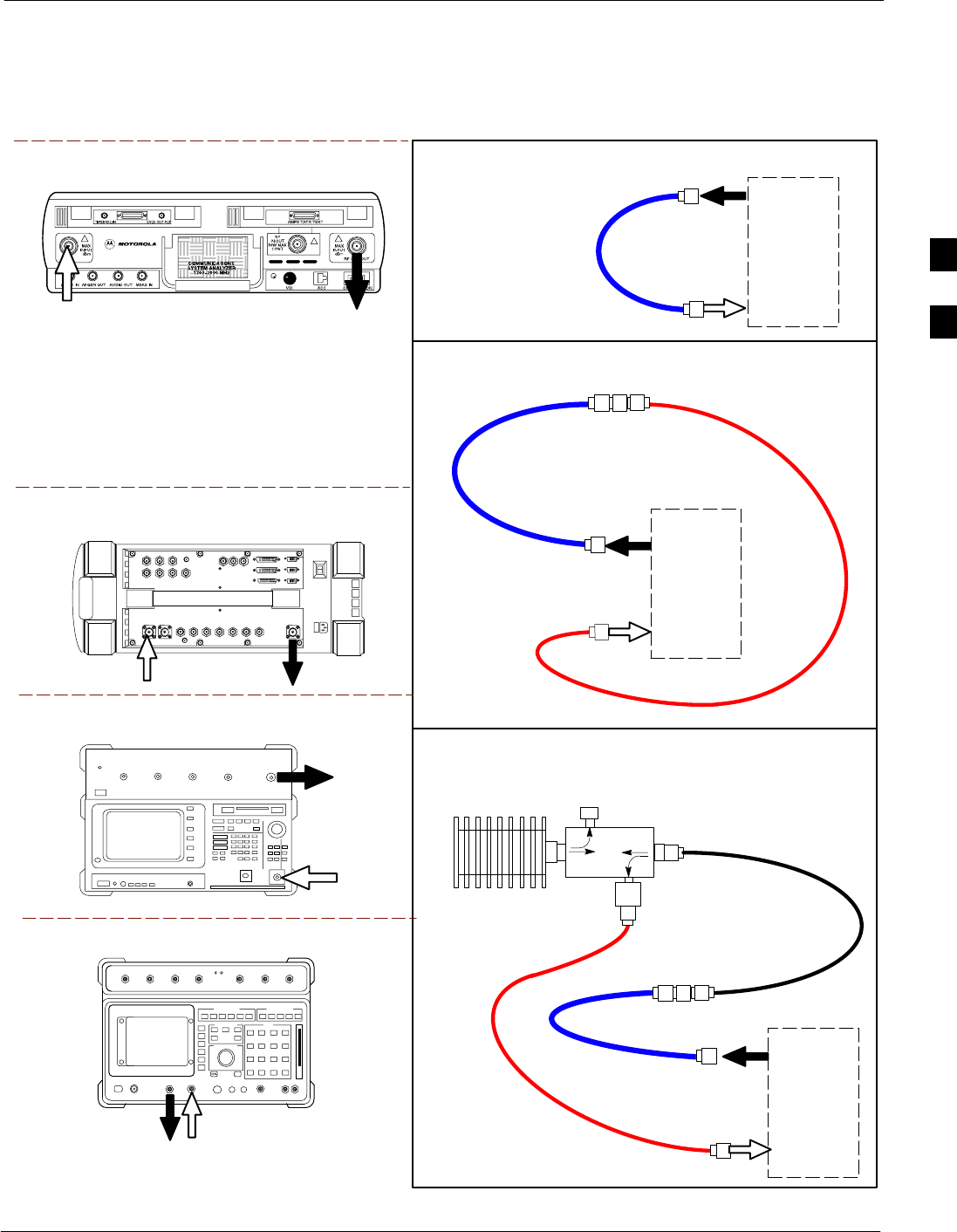
Test Equipment Set-up68P09255A69-3
Aug 2002 1X SCt4812ET Lite BTS Optimization/ATP Software Release 2.16.1.x
PRELIMINARY
3-53
Figure 3-10: IS- 95A/B Cable Calibration Test Setup - CyberTest, Agilent 8935, Advantest R3465, and
HP 8921A
Motorola CyberTest
Advantest Model R3465
RF OUT 50Ω
INPUT 50Ω
RF GEN OUTANT IN
SUPPORTED TEST SETS
100-W ATT (MIN)
NON-RADIATING
RF LOAD
TEST
SET
A. SHORT CABLE CAL
SHORT
CABLE
B. RX TEST CAL SETUP FOR TRDC
TEST
SET
C. TX TEST AND DRDC RX TEST CAL SETUP
20 DB IN-LINE
ATTENUATOR
CALIBRATION SET UP
N-N FEMALE
ADAPTER
TX
CABLE
SHORT
CABLE
Note: The 30 dB directional coupler is not used
with the Cybertest test set. The TX cable is
connected directly to the Cybertest test set.
A 10dB attenuator must be used with the short test
cable for cable calibration with the CyberTest test
set. The 10dB attenuator is used only for the cable
calibration procedure, not with the test cables for
TX calibration and ATP tests.
TEST
SET
RX
CABLE
SHORT
CABLE
DIRECTIONAL
COUPLER
(30 DB)
N-N FEMALE
ADAPTER
50 Ω
ΤERM.
Agilent 8935 Series E6380A
(formerly HP 8935)
RF
IN/OUT
ANT
IN
Hewlett Packard Model HP 8921A
Note: For 800 MHZ only. The HP8921A cannot
be used to calibrate cables for PCS frequencies.
TX CABLE FOR
TX TEST CABLE
CALIBRATION
RX CABLE FOR
DRDC RX TEST
CABLE CALIBRATION
DUPLEX
OUT ANT
IN
3
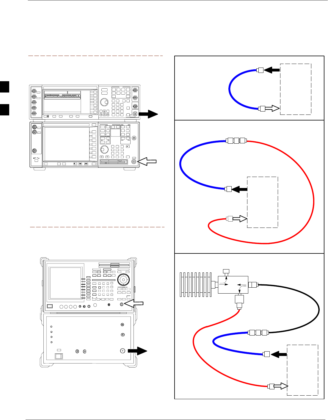
Test Equipment Set-up 68P09255A69-3
Aug 2002
1X SCt4812ET Lite BTS Optimization/ATP Software Release 2.16.1.x
PRELIMINARY
3-54
Figure 3-11: IS-95A/B and CDMA 2000 1X Cable Calibration Test Setup - Agilent E4406A/E4432B and
Advantest R3267/R3562
TEST
SET
A. SHORT CABLE CAL
SHORT
CABLE
B. RX TEST SETUP FOR TRDC
CALIBRATION SET UP
TEST
SET
RX
CABLE
SHORT
CABLE
N-N FEMALE
ADAPTER
SUPPORTED TEST SETS
INPUT 50 Ω
RF OUT
50 Ω
Advantest R3267 (Top) and R3562 (Bottom)
NOTE:
SYNTHE REF IN ON REAR OF SIGNAL GENERATOR IS
CONNECTED TO 10 MHZ OUT ON REAR OF SPECTRUM
ANALYZER
Agilent E4432B (Top) and E4406A (Bottom)
NOTE:
10 MHZ IN ON REAR OF SIGNAL GENERATOR IS CONNECTED TO
10 MHZ OUT (SWITCHED) ON REAR OF TRANSMITTER TESTER
(FIGURE F-16).
RF INPUT
50 Ω
RF OUTPUT
50 Ω
100-W ATT (MIN)
NON-RADIATING
RF LOAD
TEST
SET
D. TX TEST SETUP AND DRDC RX TEST SETUP
20 DB IN-LINE
ATTENUATOR
N-N FEMALE
ADAPTER
TX
CABLE
SHORT
CABLE
DIRECTIONAL
COUPLER
(30 DB)
50 Ω
ΤERM.
TX CABLE FOR
TX TEST CABLE
CALIBRATION
RX CABLE FOR
DRDC RX TEST
CABLE CALIBRATION
3
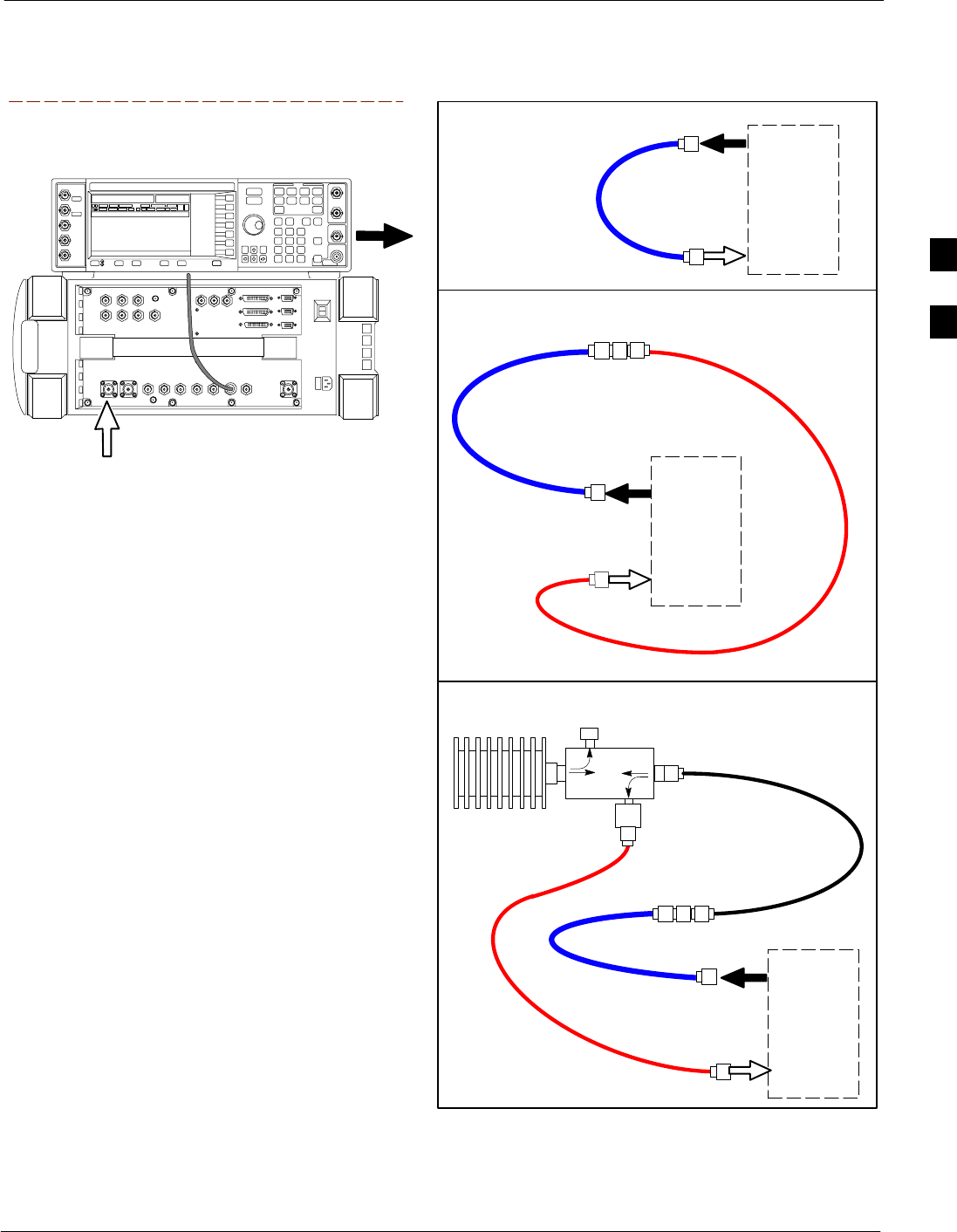
Test Equipment Set-up68P09255A69-3
Aug 2002 1X SCt4812ET Lite BTS Optimization/ATP Software Release 2.16.1.x
PRELIMINARY
3-55
TEST
SET
A. SHORT CABLE CAL
SHORT
CABLE
B. RX TEST SETUP FOR TRDC
CALIBRATION SET UP
TEST
SET
RX
CABLE
SHORT
CABLE
N-N FEMALE
ADAPTER
Figure 3-12: CDMA2000 1X Cable Calibration Test Setup - Agilent 8935/E4432B
SUPPORTED TEST SETS
Agilent E4432B (Top) and 8935 Series
E6380A (Bottom)
NOTE:
10 MHZ IN ON REAR OF SIGNAL GENERATOR IS CONNECTED TO
10 MHZ REF OUT ON SIDE OF CDMA BASE STATION TEST SET
(FIGURE F-15).
RF OUTPUT
50 Ω
100-W ATT (MIN)
NON-RADIATING
RF LOAD
TEST
SET
D. TX TEST SETUP AND DRDC RX TEST SETUP
20 DB IN-LINE
ATTENUATOR
N-N FEMALE
ADAPTER
TX
CABLE
SHORT
CABLE
DIRECTIONAL
COUPLER
(30 DB)
50 Ω
ΤERM.
TX CABLE FOR
TX TEST CABLE
CALIBRATION
RX CABLE FOR
DRDC RX TEST
CABLE CALIBRATION
ANT
IN
3
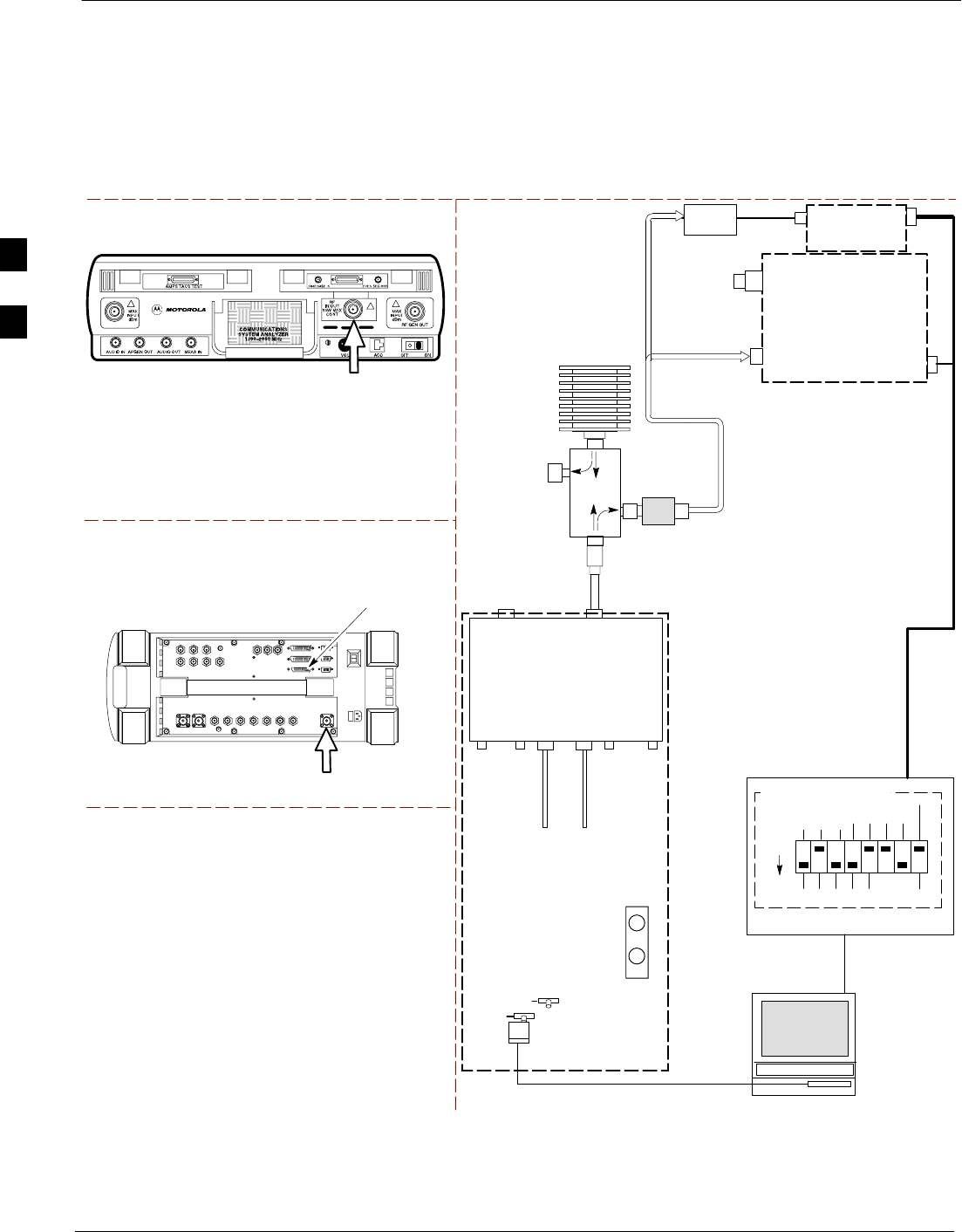
Test Equipment Set-up 68P09255A69-3
Aug 2002
1X SCt4812ET Lite BTS Optimization/ATP Software Release 2.16.1.x
PRELIMINARY
3-56
Set-up for TX Calibration
Figure 3-13 and Figure 3-14 show the test set connections for TX
calibration.
Figure 3-13: TX Calibration Test Setup - CyberTest (IS-95A/B) and Agilent 8935 (IS-95A/B and
CDMA2000 1X)
Motorola CyberTest
Agilent 8935 Series E6380A (formerly HP 8935)
TEST SETS TRANSMIT (TX) SET UP
FRONT PANEL
RF
IN/OUT
RF
IN/OUT
HP-IB
TO GPIB
BOX
NOTE: THE 30 DB DIRECTIONAL COUPLER IS NOT USED WITH THE
CYBERTEST TEST SET. THE TX CABLE IS CONNECTED DIRECTLY
TO THE CYBERTEST TEST SET.
TO
MPC
TO LPA
TRUNKING
MODULE
RS232-GPIB
INTERFACE BOX
INTERNAL PCMCIA
ETHERNET CARD
GPIB
CABLE
UNIVERSAL TWISTED PAIR (UTP)
CABLE (RJ45 CONNECTORS)
RS232 NULL
MODEM
CABLE
S MODE
DATA FORMAT
BAUD RATE
GPIB ADRS G MODE
ON
BTS
INTERNAL
TX
CABLE
CDMA
LMF
DIP SWITCH SETTINGS
10BASET/
10BASE2
CONVERTER
LAN
B
LAN
A
GPIB
RF IN/OUT
RX
ANTENNA
CONNECTOR
FREQ
MONITOR
SYNC
MONITOR
CSM
INTERNAL
RX
CABLE
TX
ANT
CPLD
RX
BTS
CPLD
TRDC
TX
BTS
CPLD
RX
ANT
CPLD
TX
ANTENNA
CONNECTOR
COMMUNICATIONS
SYSTEM ANALYZER
2O DB IN-LINE
ATTENUATOR
50 Ω
TERM
.
TX TEST
CABLE
DIRECTIONAL
COUPLER
(30 DB)
100-W ATT (MIN.)
NON-RADIATING
RF LOAD
TX TEST
CABLE
* BLACK RECTANGLES
REPRESENT THE RAISED
PART OF SWITCHES
NOTE: IF BTS IS EQUIPPED
WITH DRDCS (DUPLEXED
RX/TX SIGNALS), CONNECT
THE TX TEST CABLE TO
THE DRDC ANTENNA
CONNECTOR.
POWER
METER
(OPTIONAL)*
POWER
SENSOR
* A POWER METER CAN BE USED IN
PLACE OF THE COMMUNICATIONS
TEST SET FOR TX CALIBRATION/
AUDIT
3
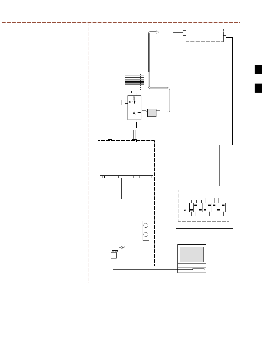
Test Equipment Set-up68P09255A69-3
Aug 2002 1X SCt4812ET Lite BTS Optimization/ATP Software Release 2.16.1.x
PRELIMINARY
3-57
Figure 3-14: TX Calibration Test Setup - Using Power Meter
TEST SETS TRANSMIT (TX) SET UP
NOTE: THE HP8921A AND ADVANTEST
R3465 CANNOT BE USED FOR TX
CALIBRATION. A POWER METER MUST BE
USED.
TO
MPC
TO LPA
TRUNKING
MODULE
RS232-GPIB
INTERFACE BOX
INTERNAL PCMCIA
ETHERNET CARD
GPIB
CABLE
UNIVERSAL TWISTED PAIR (UTP)
CABLE (RJ45 CONNECTORS)
RS232 NULL
MODEM
CABLE
S MODE
DATA FORMAT
BAUD RATE
GPIB ADRS G MODE
ON
BTS
INTERNAL
TX
CABLE
CDMA
LMF
DIP SWITCH SETTINGS
10BASET/
10BASE2
CONVERTER
LAN
B
LAN
A
RX
ANTENNA
CONNECTOR
FREQ
MONITOR
SYNC
MONITOR
CSM
INTERNAL
RX
CABLE
TX
ANT
CPLD
RX
BTS
CPLD
TRDC
TX
BTS
CPLD
RX
ANT
CPLD
TX
ANTENNA
CONNECTOR
50 Ω
TERM
.
TX TEST
CABLE
DIRECTIONAL
COUPLER
(30 DB)
100-W ATT (MIN.)
NON-RADIATING
RF LOAD
TX TEST
CABLE
* BLACK RECTANGLES
REPRESENT THE RAISED
PART OF SWITCHES
NOTE: IF BTS IS EQUIPPED
WITH DRDCS (DUPLEXED
RX/TX SIGNALS), CONNECT
THE TX TEST CABLE TO
THE DRDC ANTENNA
CONNECTOR.
POWER
SENSOR POWER METER
2O DB IN-LINE
ATTENUATOR
3
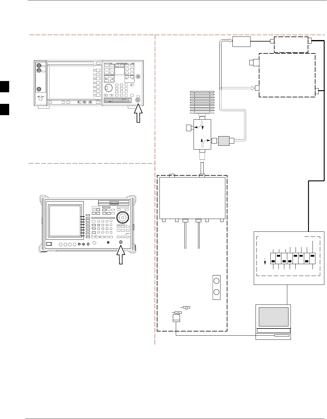
Test Equipment Set-up 68P09255A69-3
Aug 2002
1X SCt4812ET Lite BTS Optimization/ATP Software Release 2.16.1.x
PRELIMINARY
3-58
Figure 3-15: TX Calibration Test Setup - Agilent E4406A and Advantest R3567 (IS-95A/B and
CDMA2000 1X)
TEST SETS TRANSMIT (TX) SET UP
TO
MPC
TO LPA
TRUNKING
MODULE
RS232-GPIB
INTERFACE BOX
INTERNAL PCMCIA
ETHERNET CARD
GPIB
CABLE
UNIVERSAL TWISTED PAIR (UTP)
CABLE (RJ45 CONNECTORS)
RS232 NULL
MODEM
CABLE
S MODE
DATA FORMAT
BAUD RATE
GPIB ADRS G MODE
ON
BTS
INTERNAL
TX
CABLE
CDMA
LMF
DIP SWITCH SETTINGS
10BASET/
10BASE2
CONVERTER
LAN
B
LAN
A
GPIB
RF INPUT 50 Ω
OR INPUT 50 Ω
RX
ANTENNA
CONNECTOR
FREQ
MONITOR
SYNC
MONITOR
CSM
INTERNAL
RX
CABLE
TX
ANT
CPLD
RX
BTS
CPLD
TRDC
TX
BTS
CPLD
RX
ANT
CPLD
TX
ANTENNA
CONNECTOR
COMMUNICATIONS
SYSTEM ANALYZER
50 Ω
TERM
.
TX TEST
CABLE
DIRECTIONAL
COUPLER
(30 DB)
100-W ATT (MIN.)
NON-RADIATING
RF LOAD
TX TEST
CABLE
* BLACK RECTANGLES
REPRESENT THE RAISED
PART OF SWITCHES
NOTE: IF BTS IS EQUIPPED
WITH DRDCS (DUPLEXED
RX/TX SIGNALS), CONNECT
THE TX TEST CABLE TO
THE DRDC ANTENNA
CONNECTOR.
POWER
METER
(OPTIONAL)*
POWER
SENSOR
* A POWER METER CAN BE USED IN
PLACE OF THE COMMUNICATIONS
TEST SET FOR TX CALIBRATION/
AUDIT
RF INPUT
50 Ω
Agilent E4406A
INPUT 50 Ω
Advantest R3267
2O DB IN-LINE
ATTENUATOR
3
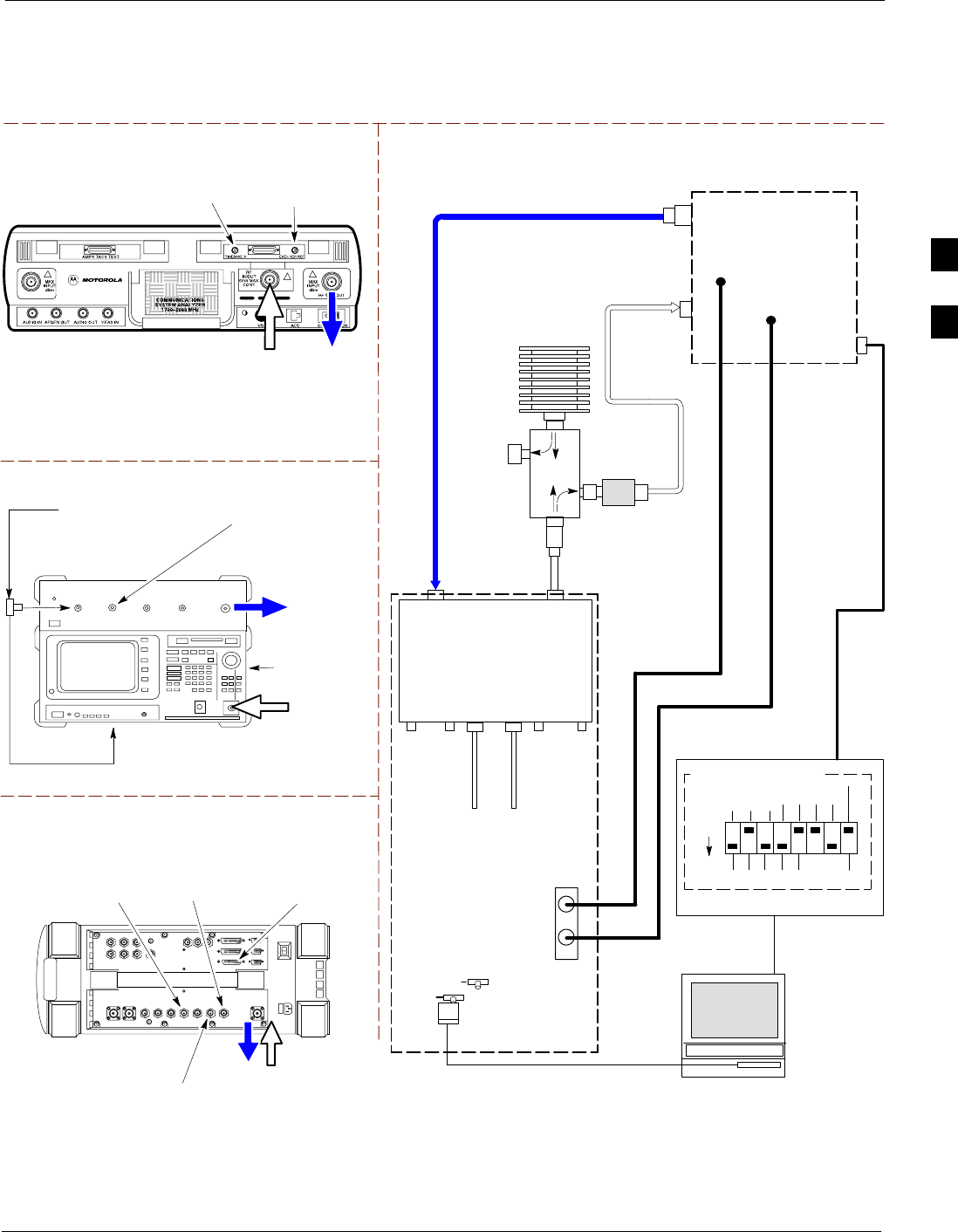
Test Equipment Set-up68P09255A69-3
Aug 2002 1X SCt4812ET Lite BTS Optimization/ATP Software Release 2.16.1.x
PRELIMINARY
3-59
Set-up for ATP
Figure 3-16 and Figure 3-17 show the test set connections for ATP tests.
Figure 3-16: IS-95A/B ATP Test Set-up, TRDC Shown - CyberTest, Advantest R3465, and Agilent 8935
Motorola CyberTest
TEST SETS Optimization/ATP SET UP
RF
IN/OUT
SYNC MONITOR
EVEN SEC TICK
PULSE REFERENCE
FROM CSM BOARD
FREQ MONITOR
19.6608 MHZ CLOCK
REFERENCE FROM
CSM BOARD
Advantest Model R3465
INPUT 50Ω
GPIB CONNECTS
TO BACK OF UNIT
NOTE: The 30 dB directional coupler is not
used with the Cybertest test set. The TX
cable is connected directly to the Cybertest
test set.
RF OUT 50Ω
FREQ MONITOR
19.6608 MHZ CLOCK
REFERENCE FROM
CSM BOARD
RF GEN
OUT
SYNC MONITOR EVEN
SEC TICK PULSE
REFERENCE FROM
CSM BOARD
BNC
“T”
TO EXT TRIGGER CONNECTOR
ON REAR OF TEST SET
(FOR DETAILS, SEE
FIGURE F-13)
TO
MPC
TO LPA
TRUNKING
MODULE
RS232-GPIB
INTERFACE BOX
INTERNAL PCMCIA
ETHERNET CARD
GPIB
CABLE
UNIVERSAL TWISTED PAIR (UTP)
CABLE (RJ45 CONNECTORS)
RS232 NULL
MODEM
CABLE
S MODE
DATA FORMAT
BAUD RATE
GPIB ADRS G MODE
ON
BTS
INTERNAL
TX
CABLE
CDMA
LMF
DIP SWITCH SETTINGS
10BASET/
10BASE2
CONVERTER
LAN
B
LAN
A
RX TEST
CABLE
GPIB
RF IN/OUT
OR
INPUT 50 Ω
RF GEN OUT,
RF OUT 50Ω,
OR RF IN/OUT
RX
ANTENNA
CONNECTOR
FREQ
MONITOR
SYNC
MONITOR
CSM
INTERNAL
RX
CABLE
TX
ANT
CPLD
RX
BTS
CPLD
TRDC
TX
BTS
CPLD
RX
ANT
CPLD
TX
ANTENNA
CONNECTOR
COMMUNICATIONS
SYSTEM ANALYZER
50 Ω
TERM
.
TX TEST
CABLE
DIRECTIONAL
COUPLER
(30 DB)
100-W ATT (MIN.)
NON-RADIATING
RF LOAD
TX TEST
CABLE
* BLACK RECTANGLES
REPRESENT THE RAISED
PART OF SWITCHES
CDMA
TIMEBASE
IN
EVEN
SECOND/
SYNC IN
NOTE: IF BTS IS EQUIPPED
WITH DRDCS (DUPLEXED RX/TX
SIGNALS), BOTH THE TX AND RX
TEST CABLES CONNECT TO THE
DRDC ANTENNA CONNECTOR.
(SEE FIGURE 3-18.)
2O DB IN-LINE
ATTENUATOR
IMPORTANT:
WHEN PERFORMING FER TEST ON COMPANION FRAME DIVERSITY RX, CONNECT
RX TEST CABLE TO RX ANTENNA PORT ON COLLOCATED COMPANION FRAME.
Agilent 8935 Series E6380A (formerly HP 8935)
RF IN/OUT
HP-IB
TO GPIB
BOX
SYNC MONITOR
EVEN SEC TICK
PULSE REFERENCE
FROM CSM BOARD
FREQ MONITOR
19.6608 MHZ CLOCK
REFERENCE FROM
CSM BOARD
10 MHZ
REF OUT
3
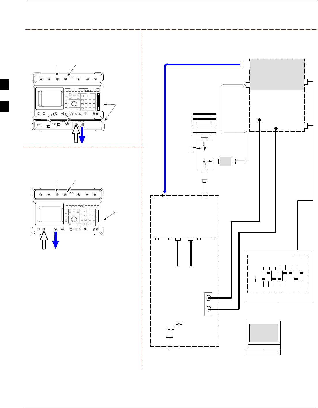
Test Equipment Set-up 68P09255A69-3
Aug 2002
1X SCt4812ET Lite BTS Optimization/ATP Software Release 2.16.1.x
PRELIMINARY
3-60
Figure 3-17: IS-95A/B ATP Test Setup - HP 8921A
RF OUT
ONLY
Hewlett Packard Model HP 8921A W/PCS Interface
(for 1900 MHz)
GPIB
CONNECTS
TO BACK OF
UNITS
SYNC MONITOR
EVEN SEC TICK
PULSE REFERENCE
FROM CSM BOARD
FREQ MONITOR
19.6608 MHZ CLOCK
REFERENCE FROM
CSM BOARD
TEST SETS Optimization/ATP SET UP
RF
IN/OUT
GPIB
CONNECTS
TO BACK OF
UNIT
SYNC MONITOR
EVEN SEC TICK
PULSE REFERENCE
FROM CSM BOARD
FREQ MONITOR
19.6608 MHZ CLOCK
REFERENCE FROM
CSM BOARD
Hewlett Packard Model HP 8921A
(for 800 MHz)
RF
IN/OUT
DUPLEX
OUT
TO
MPC
TO LPA
TRUNKING
MODULE
RS232-GPIB
INTERFACE BOX
INTERNAL PCMCIA
ETHERNET CARD
GPIB
CABLE
UNIVERSAL TWISTED PAIR (UTP)
CABLE (RJ45 CONNECTORS)
RS232 NULL
MODEM
CABLE
S MODE
DATA FORMAT
BAUD RATE
GPIB ADRS G MODE
ON
BTS
INTERNAL
TX
CABLE
CDMA
LMF
DIP SWITCH SETTINGS
10BASET/
10BASE2
CONVERTER
LAN
B
LAN
A
RX TEST
CABLE
GPIB
PCS INTERFACE
INPUT/OUTPUT
PORTS
RX
ANTENNA
CONNECTOR
FREQ
MONITOR
SYNC
MONITOR
CSM
INTERNAL
RX
CABLE
TX
ANT
CPLD
RX
BTS
CPLD
TRDC
TX
BTS
CPLD
RX
ANT
CPLD
TX
ANTENNA
CONNECTOR
COMMUNICATIONS
SYSTEM ANALYZER
50 Ω
TERM
.
TX TEST
CABLE
DIRECTIONAL
COUPLER
(30 DB)
100-W ATT (MIN.)
NON-RADIATING
RF LOAD
TX TEST
CABLE
* BLACK RECTANGLES
REPRESENT THE RAISED
PART OF SWITCHES
CDMA
TIMEBASE
IN EVEN
SECOND/
SYNC IN
NOTE: IF BTS IS EQUIPPED
WITH DRDCS (DUPLEXED
RX/TX SIGNALS), BOTH THE
TX AND RX TEST CABLES
CONNECT TO THE DRDC
ANTENNA CONNECTOR.
(SEE FIGURE 3-18.)
HP PCS
INTERFACE*
2O DB IN-LINE
ATTENUATOR
* FOR 1900 MHZ
ONLY
RF OUT ONLY
RF IN/OUT
NOTE:
FOR 800 MHZ TESTING, CONNECT CABLES TO THE
HP 8921A AS FOLLOWS:
RX TEST CABLE TO DUPLEX OUT
TX TEST CABLE TO RF IN/OUT
IMPORTANT:
WHEN PERFORMING FER TEST ON COMPANION FRAME DIVERSITY RX,
CONNECT RX TEST CABLE TO RX ANTENNA PORT ON COLLOCATED COMPANION
FRAME.
3
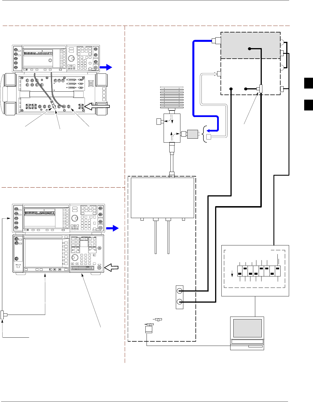
Test Equipment Set-up68P09255A69-3
Aug 2002 1X SCt4812ET Lite BTS Optimization/ATP Software Release 2.16.1.x
PRELIMINARY
3-61
Figure 3-18: IS-95A/B and CDMA2000 1X ATP Test Setup With DRDCs - Agilent Test Equipment
TEST SETS Optimization/ATP SET UP
RF INPUT
50 Ω
RF
OUTPUT
50 Ω
Agilent E4432B (Top) and E4406A (Bottom)
FREQ MONITOR
19.6608 MHZ CLOCK
REFERENCE FROM
CSM BOARD
SYNC MONITOR
EVEN SEC TICK
PULSE REFERENCE
FROM CSM BOARD
BNC
“T”
TO TRIGGER IN
ON REAR OF
TRANSMITTER
TESTER
TO PATTERN TRIG IN
ON REAR OF SIGNAL
GENERATOR
TO EXT REF IN
ON REAR OF
TRANSMITTER
TESTER
NOTE:
10 MHZ IN ON REAR OF SIGNAL GENERATOR IS CONNECTED TO
10 MHZ OUT (SWITCHED) ON REAR OF TRANSMITTER TESTER
(SEE FIGURE F-16).
TO
MPC
TO LPA
TRUNKING
MODULE
RS232-GPIB
INTERFACE BOX
INTERNAL PCMCIA
ETHERNET CARD
GPIB
CABLE
UNIVERSAL TWISTED
PAIR (UTP) CABLE
(RJ45 CONNECTORS)
RS232 NULL
MODEM
CABLE
S MODE
DATA FORMAT
BAUD RATE
GPIB ADRS G MODE
ON
BTS
INTERNAL
TX
CABLE
CDMA
LMF
DIP SWITCH SETTINGS *
10BASET/
10BASE2
CONVERTER
LAN
B
LAN
A
COMMUNICATIONS
SYSTEM ANALYZER
HP-IB
OR
GPIB
FREQ
MONITOR
SYNC
MONITOR
CSM
INTERNAL
RX
CABLE
DRDC
BTS
CPLD
ANT
CPLD
SIGNAL GENERATOR
GPIB
10 MHZ
IN
10 MHZ
REF OUT
OR
10 MHZ
OUT
TRIGGER IN
OR
EVEN SEC
SYNCH IN
EXT
REF
IN
BNC
“T”
PATTERN
TRIG IN
* BLACK RECTANGLES
REPRESENT THE RAISED
PART OF SWITCHES
DUPLEXED
TX/RX
ANTENNA
CONNECTOR
RX TEST
CABLE
50 Ω
TERM
.
TX TEST
CABLE
DIRECTIONAL
COUPLER
(30 DB)
100-W ATT (MIN.)
NON-RADIATING
RF LOAD
TX TEST
CABLE
2O DB IN-LINE
ATTENUATOR
RF IN/OUT
OR
RF INPUT
50 Ω
RF OUTPUT 50 Ω
IMPORTANT:
WHEN PERFORMING FER TEST ON
COMPANION FRAME DIVERSITY RX,
CONNECT RX TEST CABLE TO
ANTENNA PORT ON COLLOCATED
COMPANION FRAME.
Agilent E4432B (Top) and 8935 Series E6380A
(Bottom)
SYNC MONITOR
EVEN SEC TICK
PULSE REFERENCE
FROM CSM BOARD
FREQ MONITOR
19.6608 MHZ CLOCK
REFERENCE FROM
CSM BOARD
RF
OUTPUT
50 Ω
NOTES:
10 MHZ IN ON REAR OF SIGNAL GENERATOR IS CONNECTED TO
10 MHZ REF OUT ON SIDE OF CDMA BASE STATION TEST SET
PATTERN TRIG IN ON REAR OF SIGNAL GENERATOR IS
CONNECTED TO EVEN SECOND SYNC IN ON SIDE OF CDMA BASE
STATION TEST SET.
(SEE FIGURE F-15)
RF
IN/OUT
BNC
“T”
3
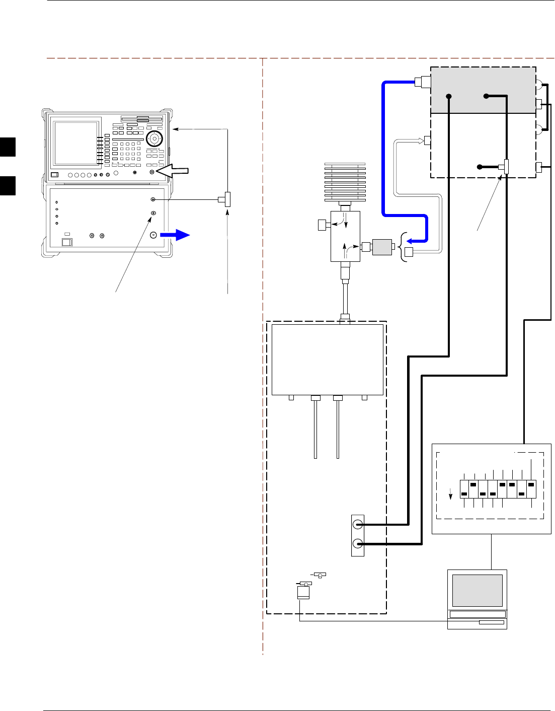
Test Equipment Set-up 68P09255A69-3
Aug 2002
1X SCt4812ET Lite BTS Optimization/ATP Software Release 2.16.1.x
PRELIMINARY
3-62
Figure 3-19: IS-95A/B and CDMA2000 1X ATP Test Setup With DRDCs - Advantest R3267/3562 Test
Equipment
TEST SETS Optimization/ATP SET UP
INPUT 50 Ω
RF OUT
50 Ω
Advantest R3267 (Top) and R3562 (Bottom)
FREQ MONITOR
19.6608 MHZ CLOCK
REFERENCE FROM
CSM BOARD
SYNC MONITOR
EVEN SEC TICK
PULSE REFERENCE
FROM CSM BOARD
BNC
“T”
NOTE:
SYNTHE REF IN ON REAR OF SIGNAL GENERATOR IS
CONNECTED TO 10 MHZ REF OUT ON REAR OF
SPECTRUM ANALYZER (SEE FIGURE F-17)
TO EXT TRIG
ON REAR OF
SPECTRUM
ANALYZER
TO
MPC
TO LPA
TRUNKING
MODULE
RS232-GPIB
INTERFACE BOX
INTERNAL PCMCIA
ETHERNET CARD
GPIB
CABLE
UNIVERSAL TWISTED
PAIR (UTP) CABLE
(RJ45 CONNECTORS)
RS232 NULL
MODEM
CABLE
S MODE
DATA FORMAT
BAUD RATE
GPIB ADRS G MODE
ON
BTS
INTERNAL
TX
CABLE
CDMA
LMF
DIP SWITCH SETTINGS
10BASET/
10BASE2
CONVERTER
LAN
B
LAN
A
INPUT
50 Ω
RF OUT
50 Ω
FREQ
MONITOR
SYNC
MONITOR
CSM
INTERNAL
RX
CABLE
DRDC
BTS
CPLD
ANT
CPLD
BNC
“T”
SPECTRUM
ANALYZER
GPIB
SIGNAL GENERATOR
GPIB
SYNTHE
REF
IN
10 MHZ
OUT
EXT
TRIG IN
MOD TIME
BASE IN
EXT TRIG
* BLACK RECTANGLES
REPRESENT THE RAISED
PART OF SWITCHES
DUPLEXED
TX/RX
ANTENNA
CONNECTOR
RX TEST
CABLE
50 Ω
TERM
.
TX TEST
CABLE
DIRECTIONAL
COUPLER
(30 DB)
100-W ATT (MIN.)
NON-RADIATING
RF LOAD
TX TEST
CABLE
2O DB IN-LINE
ATTENUATOR
IMPORTANT:
WHEN PERFORMING FER TEST ON
COMPANION FRAME DIVERSITY RX,
CONNECT RX TEST CABLE TO
ANTENNA PORT ON COLLOCATED
COMPANION FRAME.
3
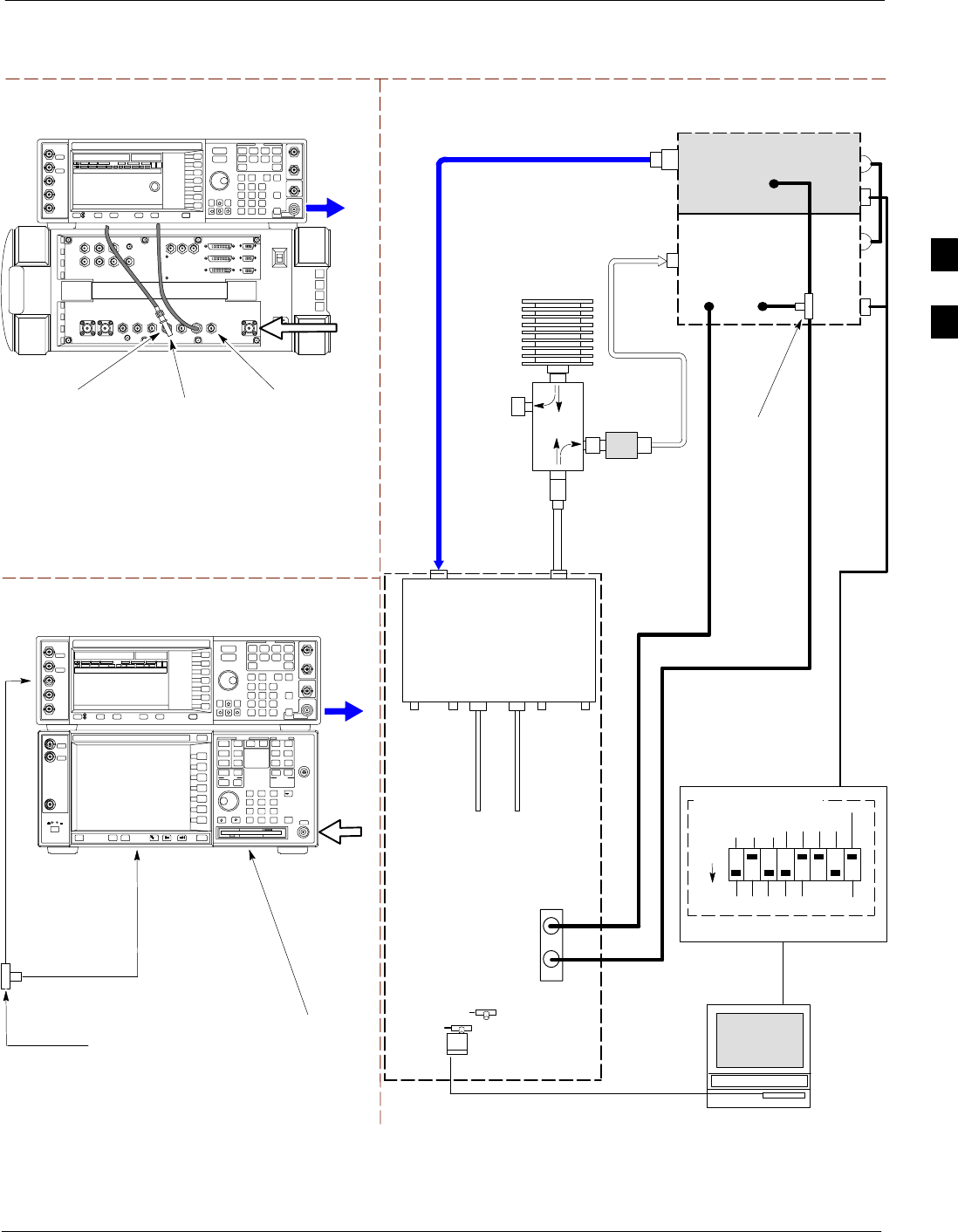
Test Equipment Set-up68P09255A69-3
Aug 2002 1X SCt4812ET Lite BTS Optimization/ATP Software Release 2.16.1.x
PRELIMINARY
3-63
Figure 3-20: IS-95A/B and CDMA2000 1X ATP Test Setup With TRDCs - Agilent Test Equipment
TEST SETS Optimization/ATP SET UP
TO
MPC
TO LPA
TRUNKING
MODULE
RS232-GPIB
INTERFACE BOX
INTERNAL PCMCIA
ETHERNET CARD
GPIB
CABLE
UNIVERSAL TWISTED
PAIR (UTP) CABLE
(RJ45 CONNECTORS)
RS232 NULL
MODEM
CABLE
S MODE
DATA FORMAT
BAUD RATE
GPIB ADRS G MODE
ON
BTS
INTERNAL
TX
CABLE
CDMA
LMF
DIP SWITCH SETTINGS
10BASET/
10BASE2
CONVERTER
LAN
B
LAN
A
RX TEST
CABLE
COMMUNICATIONS
SYSTEM ANALYZER
GPIB
RF IN/OUT
OR RF INPUT 50 Ω
RF OUTPUT 50 Ω
RX
ANTENNA
CONNECTOR
FREQ
MONITOR
SYNC
MONITOR
CSM
INTERNAL
RX
CABLE
TX
ANT
CPLD
RX
BTS
CPLD
TRDC
TX
BTS
CPLD
RX
ANT
CPLD
TX
ANTENNA
CONNECTOR
RF INPUT
50 Ω
RF
OUTPUT
50 Ω
Agilent E4432B (Top) and E4406A (Bottom)
FREQ MONITOR
19.6608 MHZ CLOCK
REFERENCE FROM
CSM BOARD
SYNC MONITOR
EVEN SEC TICK
PULSE REFERENCE
FROM CSM BOARD
BNC
“T”
TO TRIGGER IN
ON REAR OF
TRANSMITTER
TESTER
TO PATTERN TRIG IN
ON REAR OF SIGNAL
GENERATOR
TO EXT REF IN
ON REAR OF
TRANSMITTER
TESTER
NOTE:
10 MHZ IN ON REAR OF SIGNAL GENERATOR IS CONNECTED TO
10 MHZ OUT (SWITCHED) ON REAR OF TRANSMITTER TESTER
(SEE FIGURE F-16).
SIGNAL GENERATOR
GPIB
10 MHZ
IN
10 MHZ
OUT
50 Ω
TERM
.
TX TEST
CABLE
DIRECTIONAL
COUPLER
(30 DB)
100-W ATT (MIN.)
NON-RADIATING
RF LOAD
TRIGGER IN
OR
EVEN SEC
SYNCH IN
EXT
REF
IN
TX TEST
CABLE
BNC
“T”
PATTERN
TRIG IN
* BLACK RECTANGLES
REPRESENT THE RAISED
PART OF SWITCHES
2O DB IN-LINE
ATTENUATOR
IMPORTANT:
WHEN PERFORMING FER TEST ON COMPANION FRAME DIVERSITY RX, CONNECT RX TEST
CABLE TO RX ANTENNA PORT ON COLLOCATED COMPANION FRAME.
Agilent E4432B (Top) and 8935 Series E6380A
(Bottom)
SYNC MONITOR
EVEN SEC TICK
PULSE REFERENCE
FROM CSM BOARD
FREQ MONITOR
19.6608 MHZ CLOCK
REFERENCE FROM
CSM BOARD
RF
OUTPUT
50 Ω
NOTES:
10 MHZ IN ON REAR OF SIGNAL GENERATOR IS CONNECTED TO
10 MHZ REF OUT ON SIDE OF CDMA BASE STATION TEST SET
PATTERN TRIG IN ON REAR OF SIGNAL GENERATOR IS
CONNECTED TO EVEN SECOND SYNC IN ON SIDE OF CDMA BASE
STATION TEST SET.
(SEE FIGURE F-15)
RF
IN/OUT
BNC
“T”
3
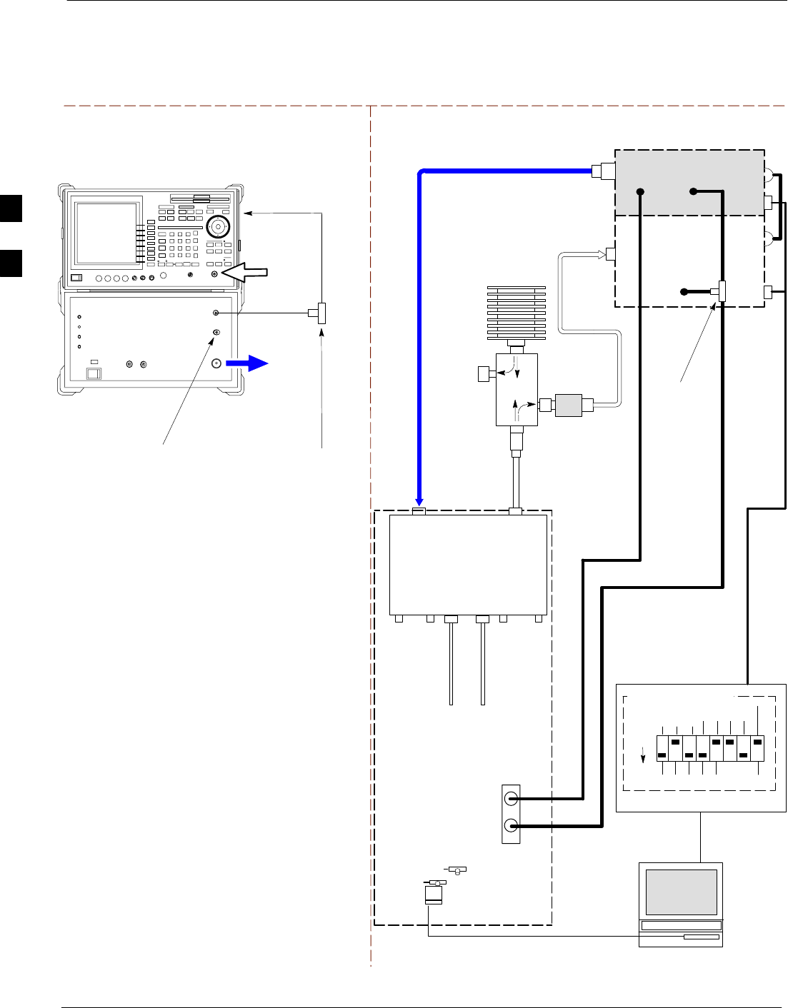
Test Equipment Set-up 68P09255A69-3
Aug 2002
1X SCt4812ET Lite BTS Optimization/ATP Software Release 2.16.1.x
PRELIMINARY
3-64
Figure 3-21: IS-95A/B and CDMA2000 1X ATP Test Setup With TRDCs - Advantest R3267/3562 Test
Equipment
TEST SETS Optimization/ATP SET UP
INPUT 50 Ω
RF OUT
50 Ω
Advantest R3267 (Top) and R3562 (Bottom)
FREQ MONITOR
19.6608 MHZ CLOCK
REFERENCE FROM
CSM BOARD
SYNC MONITOR
EVEN SEC TICK
PULSE REFERENCE
FROM CSM BOARD
BNC
“T”
NOTE:
SYNTHE REF IN ON REAR OF SIGNAL GENERATOR IS
CONNECTED TO 10 MHZ REF OUT ON REAR OF
SPECTRUM ANALYZER (SEE FIGURE F-17)
TO EXT TRIG
ON REAR OF
SPECTRUM
ANALYZER
TO
MPC
TO LPA
TRUNKING
MODULE
RS232-GPIB
INTERFACE BOX
INTERNAL PCMCIA
ETHERNET CARD
GPIB
CABLE
UNIVERSAL TWISTED
PAIR (UTP) CABLE
(RJ45 CONNECTORS)
RS232 NULL
MODEM
CABLE
S MODE
DATA FORMAT
BAUD RATE
GPIB ADRS G MODE
ON
BTS
INTERNAL
TX
CABLE
CDMA
LMF
DIP SWITCH SETTINGS
10BASET/
10BASE2
CONVERTER
LAN
B
LAN
A
RX TEST
CABLE
SPECTRUM
ANALYZER
GPIB
INPUT
50 Ω
RF OUT
50 Ω
RX
ANTENNA
CONNECTOR
FREQ
MONITOR
SYNC
MONITOR
CSM
INTERNAL
RX
CABLE
TX
ANTENNA
CONNECTOR
SIGNAL GENERATOR
GPIB
SYNTHE
REF
IN
10 MHZ
OUT
50 Ω
TERM
.
TX TEST
CABLE
DIRECTIONAL
COUPLER
(30 DB)
100-W ATT (MIN.)
NON-RADIATING
RF LOAD
EXT
TRIG IN
MOD TIME
BASE IN
TX TEST
CABLE
BNC
“T”
EXT TRIG
* BLACK RECTANGLES
REPRESENT THE RAISED
PART OF SWITCHES
TX
ANT
CPLD
RX
BTS
CPLD
TRDC
TX
BTS
CPLD
RX
ANT
CPLD
2O DB IN-LINE
ATTENUATOR
IMPORTANT:
WHEN PERFORMING FER TEST ON COMPANION FRAME DIVERSITY RX, CONNECT
RX TEST CABLE TO RX ANTENNA PORT ON COLLOCATED COMPANION FRAME.
3
Test Set Calibration68P09255A69-3
Aug 2002 1X SCt4812ET Lite BTS Optimization/ATP Software Release 2.16.1.x
PRELIMINARY
3-65
Test Set Calibration
Background
Proper test equipment calibration helps to ensure accurate BTS
optimization and acceptance testing by assuring that the test equipment
and associated cables do not introduce measurement errors.
NOTE If the test equipment set (see the Terms and Abbreviations
section of Chapter 1) being used to optimize or test the BTS has
been calibrated and maintained as a set, this procedure does not
need to be performed.
This procedure must be performed before the optimization. Verify all test
equipment (including all associated cables and adapters actually used to
interconnect test equipment items and the BTS) has been calibrated and
maintained as a set.
CAUTION If any piece of test equipment, test cable, or RF adapter, that
makes up the calibrated test equipment set has been replaced, the
set must be re-calibrated. Failure to do so can introduce
measurement errors, resulting in incorrect measurements and
degradation to system performance. Motorola recommends
repeating cable calibration before testing at each BTS site.
NOTE Calibration of the communications system analyzer (or
equivalent test equipment) must be performed at the site before
calibrating the overall test equipment set. Calibrate the test
equipment after it has been allowed to warm-up and stabilize for
a a minimum of 60 minutes.
Calibration Procedures Included
Automatic
Procedures included in this section use the LMF automated calibration
routine to determine path losses of the supported communications
analyzer, power meter, associated test cables, adapters, and (if used)
antenna switch that make up the overall calibrated test equipment set.
After calibration, the gain/loss offset values are stored in a test
measurement offset file on the LMF computer.
Manual
Agilent E4406A Transmitter Tester - The E4406A does not support
the power level zeroing calibration performed by the LMF. If this
instrument is to be used for Bay Level Offset calibration and calibration
is attempted with the LMF Calibrate Test Equipment function, the
LMF will return a status window failure message stating that zeroing
power is not supported by the E4406A. Refer to the Equipment
Calibration section of Appendix F for instructions on using the
instrument’s self-alignment (calibration) function prior to performing
Bay Level Offset calibration.
3

Test Set Calibration 68P09255A69-3
Aug 2002
1X SCt4812ET Lite BTS Optimization/ATP Software Release 2.16.1.x
PRELIMINARY
3-66
Power Meters - Manual power meter calibration procedures to be
performed prior to automated calibration are included in the Equipment
Calibration section of Appendix F.
Cable Calibration - Manual cable calibration procedures using the HP
8921A and Advantest R3465 communications system analyzers are
provided in the Manual Cable Calibration section of Appendix F, if
needed.
GPIB Addresses
GPIB addresses can range from 1 through 30. The LMF will accept any
address in that range, but the numbers entered in the LMF Options
window GPIB address boxes (Table 3-28 and Table 3-29) must match
the addresses set in the test equipment. Motorola recommends using 1
for a CDMA signal generator, 13 for a power meter, and 18 for a
communications system analyzer. To verify and, if necessary, change the
GPIB addresses of the test equipment, refer to the Setting GPIB
Addresses section of Appendix NO TAG.
Selecting Test Equipment
Serial Connection and Network Connection tabs are provided in the
LMF Options window to specify the test equipment connection method.
The Serial Connection tab is used when the test equipment items are
connected directly to the LMF computer through a GPIB box (normal
setup). The Network Connection tab is used when the test equipment is
to be connected remotely via a network connection.
Prerequisites
Be sure the following have been completed before selecting test
equipment:
STest equipment is turned on.
SGPIB addresses set in the test equipment have been verified as correct
using the applicable procedures in Appendix NO TAG.
SLMF computer serial port and test equipment are connected to the
GPIB box.
Selecting Test Equipment
Test equipment may be selected either manually with operator input or
automatically using the LMF autodetect feature.
3

Test Set Calibration68P09255A69-3
Aug 2002 1X SCt4812ET Lite BTS Optimization/ATP Software Release 2.16.1.x
PRELIMINARY
3-67
Manually Selecting Test Equipment in a Serial Connection Tab
Test equipment can be manually specified before or after the test
equipment is connected. The LMF does not attempt to verify the test
equipment is actually detected when manual selection is specified.
Follow the procedure in Table 3-28 to manually select test equipment.
Table 3-28: Selecting Test Equipment Manually in the Serial Connection Tab
Step Action
1In the LMF window menu bar, click Tools and select Options... from the pull-down menu.
- The LMF Options window appears.
2If it is not in the forefront, click on the Serial Connection tab.
3Select the correct serial port in the COMM Port: pick list (normally COM1).
4If it is not selected (black dot showing), click on the Manual Specification button.
5Click on the check box(es) corresponding to the test equipment item(s) to be used.
6Type the GPIB address in the corresponding GPIB address box (refer to the Setting GPIB Addresses
section of Appendix NO TAG for directions on verifying and/or changing test equipment GPIB
addresses).
Motorola-recommended addresses are:
1 = signal generator
13 = power meter
18 = communications system analyzer
NOTE
When test equipment items are manually selected by the operator, the LMF defaults to using a power
meter for RF power measurements. The LMF will use a communications system analyzer for RF
power measurements only if a power meter is not selected (power meter checkbox not checked).
7Click on Apply.
- The button will darken until the selection has been recorded.
NOTE
With manual selection, the LMF does not attempt to detect the test equipment to verify it is connected
and communicating with the LMF.
8Click on Dismiss to close the LMF Options window.
3

Test Set Calibration 68P09255A69-3
Aug 2002
1X SCt4812ET Lite BTS Optimization/ATP Software Release 2.16.1.x
PRELIMINARY
3-68
Automatically Selecting Test Equipment in the Serial Connection Tab
When using the auto-detection feature to select test equipment, the LMF
determines which test equipment items are actually communicating with
LMF. Follow the procedure in Table 3-29 to use the auto-detection
feature.
Table 3-29: Selecting Test Equipment Using Auto-Detect
Step Action
1In the LMF window menu bar, click Tools and select Options... from the pull-down menu.
- The LMF Options window appears.
2If it is not in the forefront, click on the Serial Connection tab.
3Select the correct serial port in the COMM Port: pick list (normally COM1).
4If it is not selected (no black dot showing), click on the Auto-Detection button.
5If they are not already displayed in the box labeled GPIB address to search, click in the box and type
in the GPIB addresses for the test equipment to be used, separating each address with commas and no
spaces. (Refer to the Setting GPIB Addresses section of Appendix NO TAG for instructions on
verifying and/or changing test equipment GPIB addresses.)
NOTE
During the GPIB address search for a test equipment item to perform RF power measurements (that is,
for TX calibration), the LMF will select the first item it finds with the capability to perform the
measurement. If, for example, the address sequence 13,18,1 is included in the GPIB addresses to
search box, the power meter (GPIB address 13) will be used for RF power measurements. If the
address sequence 18,13,1 is included, the LMF will use the communications system analyzer (GPIB
address 18) for power measurements.
6 Click Apply.
- The button will darken until the selection has been recorded.
- A check mark will appear in the applicable Manual Configuration section check boxes for
detected test equipment items.
7 Click Dismiss to close the LMF Options window.
3
Test Set Calibration68P09255A69-3
Aug 2002 1X SCt4812ET Lite BTS Optimization/ATP Software Release 2.16.1.x
PRELIMINARY
3-69
Calibrating Test Equipment
The LMF Calibrate Test Equipment function zeros the power
measurement level of the test equipment item that is to be used for TX
calibration and audit. If both a power meter and an analyzer are
connected (for example, an HP 437 and an HP8921A/600), only the
power meter is zeroed.
NOTE The Agilent E4406A transmitter tester does not support power
measurement level zeroing. Refer to the Equipment Calibration
section of Appendix F for E4406A calibration.
Prerequisites
SLMF computer serial port and test equipment are connected to the
GPIB box.
STest equipment is turned on and has warmed up for at least 60
minutes.
STest equipment has been selected in the LMF (Table 3-28 or
Table 3-29)
Follow the procedure in Table 3-30 to calibrate the test equipment.
Table 3-30: Test Equipment Calibration
Step Action
1 Click Util in the BTS menu bar, and select Calibrate Test Equipment from the pull-down menu.
-A Directions window will be displayed.
2Follow the direction provided.
3Click on Continue to close the Directions window and start the calibration process.
-A status report window is displayed.
4Click on OK to close the status report window.
Calibrating Cables - Overview
The LMF Cable Calibration function is used to measure the path loss
(in dB) for the TX and RX cables, adapters, directional couplers, and
attenuators that make up the cable configurations used for testing. A
communications system analyzer is used to measure the loss of both the
TX test cable and the RX test cable configurations. LMF cable
calibration consists of the following processes:
1. Measure the loss of a short cable. This is done to compensate for any
measurement error of the communications system analyzer. The
short cable, which is used only for the calibration process, is
connected in series with both the TX and RX test cable
configurations when they are measured. The measured loss of the
short cable is deducted from the measured loss of the TX and RX
test cable configurations to determine the actual loss of the
configurations. This deduction is done so any error in the analyzer
measurement will be adjusted out of both the TX and RX
measurements.
3
Test Set Calibration 68P09255A69-3
Aug 2002
1X SCt4812ET Lite BTS Optimization/ATP Software Release 2.16.1.x
PRELIMINARY
3-70
2. Measure the loss of the short cable plus the RX test cable
configuration. The RX test cable configuration normally consists
only of a coax cable with type-N connectors that is long enough to
reach from the BTS RX connector to the test equipment. When the
BTS antenna connectors carry duplexed TX and RX signals, a
directional coupler and, if required by BTS type, an additional
attenuator are also required for the RX test cable configuration.
These additional items must be included in the path loss
measurement.
3. Measure the loss of the short cable plus the TX test cable
configuration. The TX test cable configuration normally consists of
two coax cables with type-N connectors, a directional coupler, a
termination load with sufficient rating to dissipate the BTS output
power, and an additional attenuator, if required by the BTS type. The
total path loss of the TX test configuration must be as required for
the BTS (normally 30 or 50 dB). The Motorola Cybertest analyzer is
different from other communications system analyzers because the
required attenuation/load is built into the test set. Because of this,
the Cybertest TX test configuration consists only of the required
length coax cable.
Calibrating Test Cable Configurations with a Communications System
Analyzer
NOTE LMF cable calibration cannot be accomplished with an
HP8921A analyzer for 1.9 MHz. A different analyzer type or the
signal generator and spectrum analyzer method (Table 3-32 and
Table 3-33) must be used. Cable calibration values must be
manually entered into the LMF cable loss file if the signal
generator and spectrum analyzer method is used. To use the
HP8921A for manual test cable configuration calibration for 800
MHz BTSs, refer to the Manual Cable Calibration section of
Appendix F.
Prerequisites
STest equipment is turned on and has warmed up for at least 60
minutes.
STest equipment has been selected in the LMF (Table 3-28 or
Table 3-29).
STest equipment has been calibrated and correctly connected for the
type of test cable configuration to be calibrated.
Refer to Figure 3-10 or Figure 3-11 and follow the procedure in
Table 3-31 to calibrate the test cable configurations.
Table 3-31: Test Cable Configuration Calibration with a Communications System Analyzer
Step Action
1 Click Util in the BTS menu bar, and select Cable Calibration... in the pull-down menu.
-A Cable Calibration window is displayed.
. . . continued on next page
3
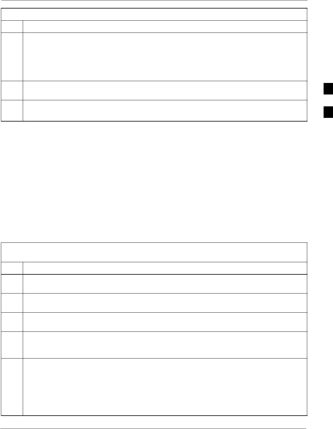
Test Set Calibration68P09255A69-3
Aug 2002 1X SCt4812ET Lite BTS Optimization/ATP Software Release 2.16.1.x
PRELIMINARY
3-71
Table 3-31: Test Cable Configuration Calibration with a Communications System Analyzer
Step Action
2Enter one or more channel numbers in the Channels box.
NOTE
Multiple channel numbers must be separated by a comma with no spaces (for example, 200,800).
When two or more channel numbers are entered, the cables will be calibrated for each channel.
Interpolation will be accomplished for other channels, as required, for TX calibration.
3 Select TX and RX CABLE CAL, TX CABLE CAL or RX CABLE CAL in the Cable Calibration
picklist.
4 Click OK, and follow the directions displayed for each step.
- A status report window will be displayed with the results of the cable calibration.
Calibrating TX and Duplexed RX ATP Test Cable Configurations Using a
Signal Generator and Spectrum Analyzer
Refer to Figure 3-22 and follow the procedure in Table 3-32 to calibrate
the TX test cable configuration for all BTSs or the RX ATP test cable
configuration for BTSs with duplexed TX/RX using the signal generator
and spectrum analyzer.
Table 3-32: Calibrating the TX Test Cable Configuration or the Duplexed RX Test Cable Configuration
Using Signal Generator and Spectrum Analyzer
Step Action
1Connect a short test cable between the spectrum analyzer and the signal generator as shown in
Figure 3-22, detail “A” (top portion of figure).
2Set signal generator to 0 dBm at the customer frequency of the 869.7-893.31 MHz band for North
American cellular and 1930-1990 MHz band for North American PCS.
3Use spectrum analyzer to measure signal generator output and record the value for the detail “A”
setup.
4Change the test setup to the one shown in detail “B” (lower portion of Figure 3-22), to measure cable
output at customer frequency (869.7-893.31 MHz band for North American cellular and 1930-1990
MHz for North American PCS) and record the value measured using the detail “B” test setup.
5Calibration factor = (value measured with detail “A” setup) - (value measured with detail “B” setup)
Example: Cal factor = -1 dBm - (-53.5 dBm) = 52.5 dB
NOTE
The short cable is used for calibration only. It is not part of the final test setup. After calibration is
completed, do not re-arrange any cables. Use the test cable configuration as-is to ensure test
procedures use the correct calibration factor.
3
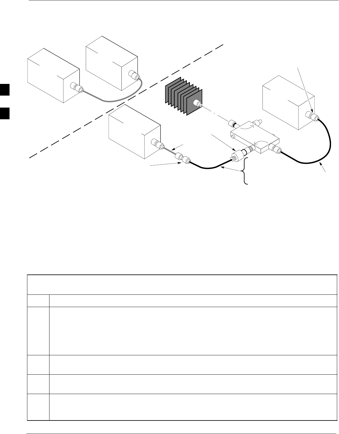
Test Set Calibration 68P09255A69-3
Aug 2002
1X SCt4812ET Lite BTS Optimization/ATP Software Release 2.16.1.x
PRELIMINARY
3-72
Figure 3-22: Calibration Setup for TX Test Cable Configuration and Duplexed RX Test Cable Configuration
Using Signal Generator and Spectrum Analyzer
50 OHM
TERMINATION
30 DB
DIRECTIONAL
COUPLER
Spectrum
Analyzer
Signal
Generator
A
Spectrum
Analyzer
40W NON-RADIATING
RF LOAD
B
SHORT TEST CABLE
Signal
Generator
THIS WILL CONNECT TO THE POWER METER OR
COMMUNICATIONS SYSTEM ANALYZER DURING TX
CALIBRATION AND TO THE COMMUNICATIONS
SYSTEM ANALYZER DURING TX AND RX ATP TESTS.
SHORT
TEST
CABLE
SECOND TX TEST CABLE
FOR TX CAL AND ATP
20DB 20 W IN-LINE
ATTENUATOR FOR
1.9 GHZ
THIS WILL CONNECT TO THE BTS TX
ANTENNA CONNECTOR DURING TX
CALIBRATION AND TO THE TX/RX ANTENNA
CONNECTORS DURING ATP TESTS.
TX TEST
CABLE
RX TEST CABLE
FOR RX ATP TEST
OR
Calibrating Non-Duplexed RX Test Cable Configuration Using a Signal
Generator and Spectrum Analyzer
Refer to Figure 3-23 and follow the procedure in Table 3-33 to calibrate
the test cable configuration for non-duplexed RX using the signal
generator and spectrum analyzer.
Table 3-33: Calibrating Non-Duplexed RX Test Cable Configuration Using a Signal Generator and Spectrum
Analyzer
Step Action
1NOTE
When preparing to calibrate a BTS with duplexed TX and RX the RX cable calibration must be done
using calibration setup in Figure 3-22 and the procedure in Table 3-32.
Connect a short test cable between the spectrum analyzer and the signal generator as shown in
Figure 3-23, detail “A” (top portion of figure).
2Set signal generator to -10 dBm at the customer’s RX frequency of 824.7-848.31 MHz for North
American cellular or 1850-1910 MHz band for North American PCS.
3Use the spectrum analyzer to measure signal generator output and record the value for the detail “A”
setup.
4Change the test setup to the one shown in detail “B” (lower portion of Figure 3-23) to measure the
output at the customer’s RX frequency (824.7-848.31 MHz for North American cellular or 1850-1910
MHz band for North American PCS). Record the value measured with the detail “B” test setup.
. . . continued on next page
3
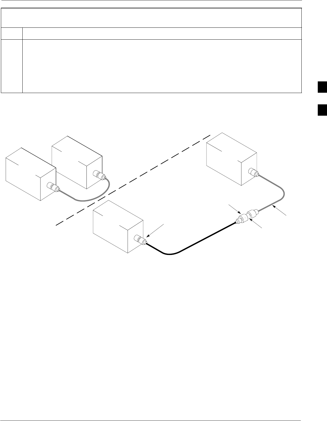
Test Set Calibration68P09255A69-3
Aug 2002 1X SCt4812ET Lite BTS Optimization/ATP Software Release 2.16.1.x
PRELIMINARY
3-73
Table 3-33: Calibrating Non-Duplexed RX Test Cable Configuration Using a Signal Generator and Spectrum
Analyzer
Step Action
5Calibration factor = (value measured with detail “A” setup) - (value measured with detail “B” setup)
Example: Cal factor = -12 dBm - (-14 dBm) = 2 dB
NOTE
The short test cable is used for test equipment setup calibration only. It is not part of the final test
setup. After calibration is completed, do not re-arrange any cables. Use the test cable configuration
as-is to ensure test procedures use the correct calibration factor.
Figure 3-23: Calibration Setup for Non-Duplexed TX/RX Antenna Connection RX Test Cable Configuration
Using Signal Generator and Spectrum Analyzer
Spectrum
Analyzer
Signal
Generator
A
B
Spectrum
Analyzer
SHORT
TEST
CABLE
CONNECTION TO THE COMMUNICATIONS
SYSTEM ANALYZER RF OUTPUT
CONNECTOR DURING RX MEASUREMENTS
Signal
Generator
BULLET
CONNECTOR
RX TEST
CABLE
SHORT TEST
CABLE
CONNECTION TO THE BTS RX ANTENNA
CONNECTOR DURING RX ATP
IMPORTANT: IF BTS TX/RX SIGNALS ARE
DUPLEXED, THE RX TEST CABLE CONNECTS
TO THE DUPLEXED ANTENNA CONNECTOR
AND MUST USE/BE CALIBRATED WITH THE 30
DB DIRECTIONAL COUPLER AND 20 DB
IN-LINE ATTENUATOR. SEE FIGURE 3-22.
3

Test Set Calibration 68P09255A69-3
Aug 2002
1X SCt4812ET Lite BTS Optimization/ATP Software Release 2.16.1.x
PRELIMINARY
3-74
Setting Cable Loss Values
Cable loss values for TX and RX test cable configurations are normally
set by accomplishing automatic cable calibration using the LMF and the
applicable test equipment. The LMF stores the measured loss values in
the cable loss files. The cable loss values can also be set or changed
manually.
CAUTION If cable calibration was performed without using the LMF, cable
loss values must be manually entered in the LMF database.
Failure to do this will result in inaccurate BTS calibration and
reduced site performance.
Prerequisites
SLMF is logged into the BTS
Table 3-34: Setting Cable Loss Values
Step Action
1 Click Util in the BTS menu bar, and select Edit > Cable Loss in the pull-down menus.
-A tabbed data entry pop-up window will appear.
2Click on the TX Cable Loss tab or the RX Cable Loss tab, as required.
3To add a new channel number, perform the following:
3a - Click on the Add Row button.
3b - Click in the Channel # or Loss (dBm) column, as required.
3c - Enter the desired value.
4To edit existing values, click in the data box to be changed and change the value.
5To delete a row, click on the row and then click on the Delete Row button.
6For each tab with changes, click on the Save button to save displayed values.
7Click on the Dismiss button to close the window.
NOTE
SValues entered or changed after the Save button was used will be lost when the window is
dismissed.
SIf cable loss values exist for two different channels the LMF will interpolate for all other channels.
SEntered values will be used by the LMF as soon as they are saved. It is not necessary to log out and
log back into the LMF for changes to take effect.
3

Test Set Calibration68P09255A69-3
Aug 2002 1X SCt4812ET Lite BTS Optimization/ATP Software Release 2.16.1.x
PRELIMINARY
3-75
Setting TX Coupler Loss Value
If an in-service TX coupler is installed, the coupler loss must be
manually entered so it will be included in the LMF TX calibration and
audit calculations.
Prerequisites
SLMF is logged into the BTS
SPath loss, in dB, of the TX coupler must be known
Table 3-35: Setting TX Coupler Loss Values
Step Action
1 Click Util in the BTS menu bar, and select Edit > Coupler Loss... in the pull-down menus.
-A tabbed data entry pop-up window will appear.
2Click on the TX Coupler Loss tab or the RX Coupler Loss tab, as required
3Click in the Loss (dBm) column for each carrier that has a coupler and enter the appropriate value.
4To edit existing values, click in the data box to be changed and change the value.
5For each tab with changes, click on the Save button to save displayed values.
6Click on the Dismiss button to close the window.
NOTE
SValues entered or changed after the Save button is used will be lost when the window is dismissed.
SThe In-Service Calibration check box in the Tools > Options > BTS Options tab must be
checked before entered TX coupler loss values will be used by the TX calibration and audit
functions.
SNew or changed values will be used by the LMF as soon as they are saved. Logging out and logging
in again are not required to cause saved changes to take effect.
3

Bay Level Offset Calibration 68P09255A69-3
Aug 2002
1X SCt4812ET Lite BTS Optimization/ATP Software Release 2.16.1.x
PRELIMINARY
3-76
Bay Level Offset Calibration
Purpose of Bay Level Offset Calibration
Bay Level Offset (BLO) calibration is the central activity of the
optimization process. BLO calibration compensates for normal
equipment variations within the BTS RF paths and assures the correct
transmit power is available at the BTS antenna connectors to meet site
performance requirements.
What is BLO Calibration?
Description
BLO calibration is the complete title of what is normally referred to as
“calibration.” Calibration identifies the accumulated gain in every
transmit path at the BTS site. The transmit path BLO values determined
during calibration are stored in the LMF calibration data file, and are
subsequently downloaded to each BBX. When transmit path calibration
is performed, receive path BLO values will automatically be set to the
default value in the LMF calibration file and downloaded.
BTS RF Path Descriptions
Transmit (TX) path - A TX path starts at an SCCP shelf BBX
backplane slot, travels through the CIO card, is routed to the Linear
Power Amplifier (LPA) trunking module for sector phase shifting,
through the LPAs, back through the LPA trunking module for sector
phase selection, through the TX bandpass filter (starter frames) or 2:1
TX combiner (companion frames), through the Transmit & Receive Dual
Directional Coupler (TRDC) or Duplexer Directional Coupler (DRDC),
and ends at the TRDC TX or DRDC antenna connector.
Receive (RX) main path - A main RX path starts at ANTENNAS
connectors 1A, 2A, or 3A and travels through the associated TRDC or
DRDC, the MPC in SCCP cage slot MPC-1, the CIO card, and
terminates at a backplane BBX slot in the SCCP shelf.
Diversity RX path - Diversity RX paths differ for SC4812ET Lite
starter (stand-alone) and companion frames. The following describe each
type of path:
SStarter frame diversity RX path - A starter frame diversity RX path
is the same as a main RX path except that it starts at ANTENNAS
connectors 1B, 2B, or 3B, travels through the associated TRDC or
DRDC, and the MPC card in SCCP cage slot MPC-2 (refer to
Table 1-5).
SCompanion frame diversity RX path - The companion frame main
RX signal is used for the collocated companion frame diversity RX
signal. A companion frame’s diversity RX path starts at ANTENNAS
connectors 1A, 2A, or 3A in the collocated companion frame. It
travels through the associated TRDC or DRDC, the MPC in SCCP
cage slot MPC-1, and the CIO card where it is then routed out of the
3

Bay Level Offset Calibration68P09255A69-3
Aug 2002 1X SCt4812ET Lite BTS Optimization/ATP Software Release 2.16.1.x
PRELIMINARY
3-77
frame through the RX expansion out connectors (RX EXPANSION
1A, 2A, or 3A in Figure 1-9 or Figure 1-10). The signal travels
through the inter-frame diversity RX cables, into the RX expansion in
ports (RX EXPANSION 1B, 2B, or 3B in Figure 1-9 or Figure 1-10)
of the companion frame, through the Expansion MPC (EMPC) in
SCCP cage slot MPC-2, the CIO, and terminates at a backplane BBX
slot in the SCCP shelf.
SRFDS sampling paths - Directional couplers for RFDS signal
sampling are integral to the SC4812ET Lite transmit and receive paths
in the DRDCs and TRDCs. Cables connect from these directional
couplers to the RFDS input connectors.
Component Verification During Calibration
TX Path Calibration
TX path calibration supports verification of correct BTS installation, RF
cabling installation and performance, functionality of all equipment
installed in the transmit RF chain, and the proper functioning of each
transmit RF path. External test equipment is used to calibrate and audit
the TX paths of the BTS.
RX Path Calibration
RX path calibration is not required or supported on CDMA BTS
systems. Default RX calibration values are written to the RX calibration
data files during the TX calibration process. RX functionality is verified
during Frame Erasure Rate (FER) testing.
When to Calibrate
Calibration to determine BLO:
1. Is required after initial BTS installation.
2. Must be done once each year for an operational BTS site.
3. Is recommended by Motorola for all associated RF paths after
replacing any of the following components:
- BBX card
- SCCP shelf
- CIO card
- CIO-to-LP A trunking module RF cable
- LPA trunking module
-LPA
- Trunking module-to-TX filter/filter combiner RF cable
- TX filter or TX filter combiner
- TX filter/filter combiner-to-DRDC/TRDC cable
- DRDC or TRDC
BLO Calibration Data File
During the calibration process, the LMF creates a calibration (CAL) data
file where BLO values are stored. After calibration has been completed,
these offset values must be downloaded to the BBXs using the LMF
BLO download function. A detailed description of the file organization
and content is provided in the following paragraphs
3
Bay Level Offset Calibration 68P09255A69-3
Aug 2002
1X SCt4812ET Lite BTS Optimization/ATP Software Release 2.16.1.x
PRELIMINARY
3-78
NOTE Due to the size of the file, Motorola recommends printing out a
copy of a bts- #.cal file and referring to it for the following
descriptions.
CAL File Organization
The CAL file is subdivided into three sections called “slot Blocks”.
These are:
1. Slot[1] Block which contains the calibration data for the six primary
BBX slots.
2. Slot[20] Block which contains the calibration data for the redundant
BBX (see Table 3-37).
3. Slot[385] Block which contains the calibration data for the RFDS.
BBX Slot Block Parts
BBX slot Blocks are further subdivided into the parts described in the
following:
Slot Block Header - Each BBX slot Block has a header section (slot
header) which contains:
SA creation Date and Time - broken down into separate parameters of
createMonth, createDay, createYear, createHour, and createMin.
SThe number of calibration entries in the file - the numBayLevelPts
parameter. The parameter is fixed at 720 entries for SC4812-series
frames. These 720 entries are combined to define the 360 calibration
points of the CAL file.
SThe slot Block format parameter.
Slot Block Bay Level Calibration Data - Each BBX slot Block has a
Bay Level Calibration data section (BayLevelCal) which is organized as
a large flat array. The array is organized by branch, SCCP cage BBX
slot, and calibration entries. There are several ways to look at the array
contents. Two different views are provided in the following to illustrate
the significant features of BayLevelCal section content and organization:
SThe first view of the array is shown in Table 3-36. This view shows
the three branches of the array, transmit, main receive, and diversity
receive offsets, and the calibration entry ranges which apply to each.
Table 3-36: BLO bts- #.cal File Array Branch Assignments
Range Branch Assignment
C[1]-C[120] Transmit
C[121]-C[240] No SC4812ET Lite BLO cal
point entries (default only)
C[241]-C[360] Receive
C[361]-C[480] No SC4812ET Lite BLO cal
point entries (default only)
C[481]-C[600] Diversity Receive
C[601]-C[720] No SC4812ET Lite BLO cal
point entries (default only)
3
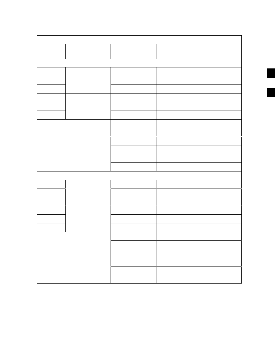
Bay Level Offset Calibration68P09255A69-3
Aug 2002 1X SCt4812ET Lite BTS Optimization/ATP Software Release 2.16.1.x
PRELIMINARY
3-79
SThe second view of the array is shown in Table 3-37. This view shows
the assignment of calibration entries in each branch to each BBX slot,
carrier, and sectorization. Three sectors are allowed for an SC4812ET
Lite frame.
Table 3-37: SC4812ET Lite bts- #.cal File Array (By BBX/Sector)
BBX Sectorization TX Branch RX Branch RX Diversity
Branch
Slot[1] (Primary BBXs 1 through 6)
1 (Omni) C[1]-C[20] C[241]-C[260] C[481]-C[500]
23-Sector, C[21]-C[40] C[261]-C[280] C[501]-C[520]
31st Carrier C[41]-C[60] C[281]-C[300] C[521]-C[540]
4 C[61]-C[80] C[301]-C[320] C[541]-C[560]
53-Sector, C[81]-C[100] C[321]-C[340] C[561]-C[580]
62nd Carrier C[101]-C[120] C[341]-C[360] C[581]-C[600]
C[121]-C[140] C[361]-C[380] C[601]-C[620]
C[141]-C[160] C[381]-C[400] C[621]-C[640]
Not Used in SC4812ET Lite
(CAL file entries are C[161]-C[180] C[401]-C[420] C[641]-C[660]
(CAL file entries are
Channel 0 with default C[181]-C[200] C[421]-C[440] C[661]-C[680]
power set level.) C[201]-C[220] C[441]-C[460] C[681]-C[700]
C[221]-C[240] C[461]-C[480] C[701]-C[720]
Slot[20] (Redundant BBX-R1)
1 (Omni) C[1]-C[20] C[241]-C[260] C[481]-C[500]
23-Sector, C[21]-C[40] C[261]-C[280] C[501]-C[520]
31st Carrier C[41]-C[60] C[281]-C[300] C[521]-C[540]
4 C[61]-C[80] C[301]-C[320] C[541]-C[560]
53-Sector, C[81]-C[100] C[321]-C[340] C[561]-C[580]
62nd Carrier C[101]-C[120] C[341]-C[360] C[581]-C[600]
C[121]-C[140] C[361]-C[380] C[601]-C[620]
C[141]-C[160] C[381]-C[400] C[621]-C[640]
Not Used in SC4812ET Lite
(CAL file entries are C[161]-C[180] C[401]-C[420] C[641]-C[660]
(CAL file entries are
Channel 0 with default C[181]-C[200] C[421]-C[440] C[661]-C[680]
power set level.) C[201]-C[220] C[441]-C[460] C[681]-C[700]
C[221]-C[240] C[461]-C[480] C[701]-C[720]
SWhen referring to the CAL file print-out and Table 3-37, it can be
seen that there is one BBX slot per sector with 20 “calibration entries”
per BBX (sector) for each branch. Two calibration entries define a
single “calibration point;” therefore there are ten calibration points in
each branch for each BBX.
- The first entry for a calibration point (all odd entries) identifies the
CDMA channel (frequency) where the BLO is measured. The
second calibration entry (all even entries) is the power set level
(PwrLvlAdj) for that frequency. The valid range for PwrLvlAdj is
3

Bay Level Offset Calibration 68P09255A69-3
Aug 2002
1X SCt4812ET Lite BTS Optimization/ATP Software Release 2.16.1.x
PRELIMINARY
3-80
from 2500 to 27500 (2500 corresponds to -125 dBm and 27500
corresponds to +125 dBm).
- The ten calibration points for each slot-branch combination must be
stored in order of increasing frequency. If less than ten points
(frequencies) are calibrated, the BLO data for the highest frequency
calibrated is written into the remainder of the ten points for that
slot-branch.
Example:
C[1]=384 (odd cal entry)
C[2]=19102 (even cal entry)
C[3]=777 (odd cal entry)
C[4]=19086 (even cal entry)
C[19]=777 (odd cal entry)
C[20]=19086 (even cal entry)
.
.
.
= 1 “calibration point”
= 1 “calibration point”
= 1 “calibration point”
In the example above, BLO was measured at only two frequencies
(channels 384 and 777) for SCCP slot BBX-1 transmit (Table 3-37).
The BLO data for the highest frequency measured (channel 777) will
be written to the remaining eight transmit calibration points (defined
by entries C[5] through C[20]) for BBX-1.
Slot Block Temperature Compensation - Each BBX slot Block also
has a temperature compensation data section (TempLevelCal) where
power level compensation factors for temperature variations are stored.
CAL File and BLO Data Download
When BLO data is downloaded to the BBXs after calibration, the data is
downloaded to the devices in the order it is stored in the CAL file. TX
calibration data (entries C[1] - C[60]) are sent first. Data for the ten
BBX slot 1 calibration points (entries C[1] - C[20]) are sent initially,
followed by data for the ten BBX slot 2 calibration points (entries C[21]
- C[40]), and so on. The RX calibration data is sent next in BBX slot
sequence, followed by RX Diversity calibration data.
Test Equipment Setup for RF Path Calibration
Follow the steps outlined in Table 3-38 and refer as needed to
Figure 3-13 or Figure 3-14 to set up test equipment.
Table 3-38: Set Up Test Equipment for RF Path Calibration
Step Action
1If it has not already been done, refer to the procedure in Table 3-10 to interface the LMF
computer terminal to the frame LAN A connector.
2If it has not already been done, refer to Table 3-11 to start a GUI LMF session.
3If required, calibrate the test equipment per the procedure in Table 3-30.
3
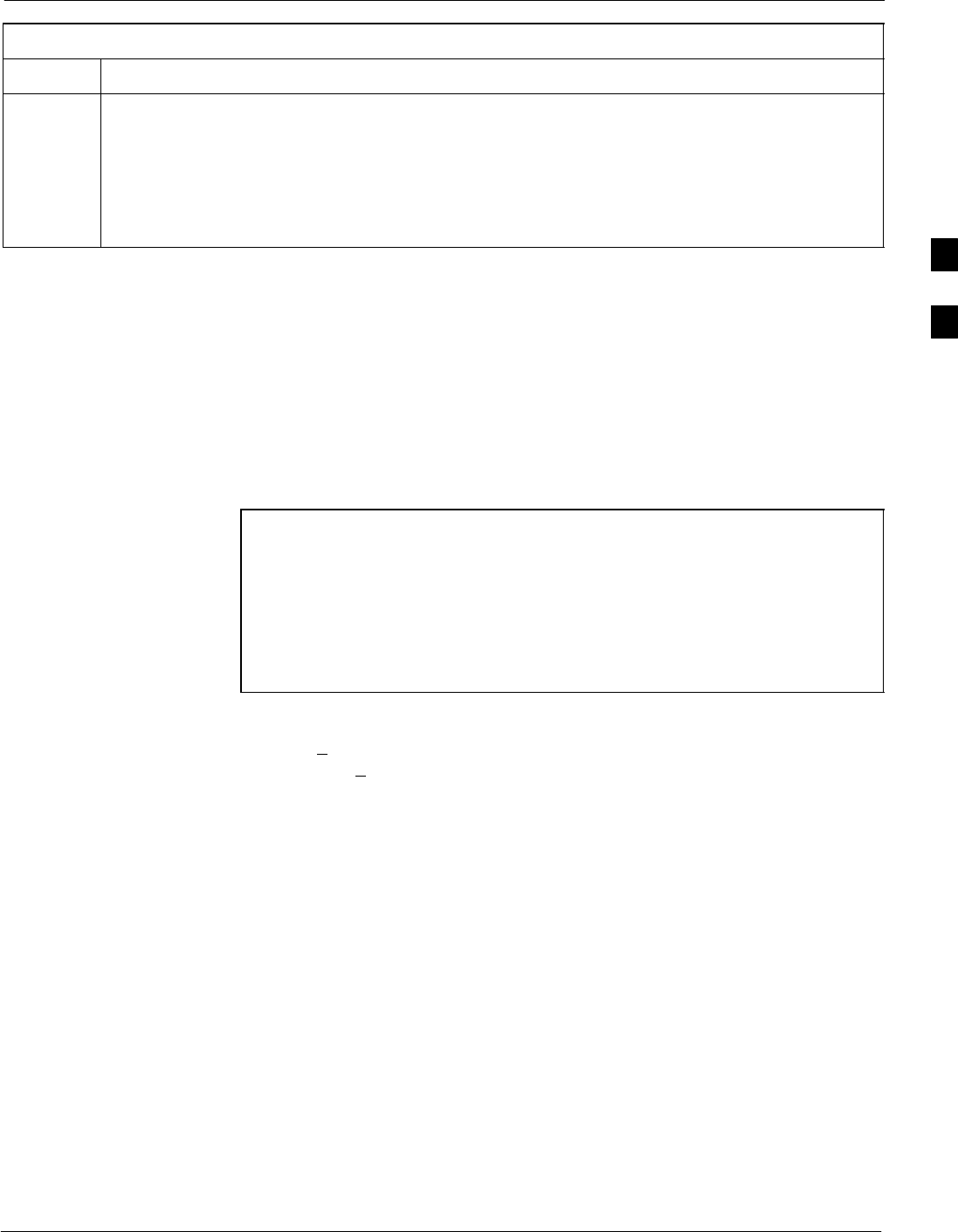
Bay Level Offset Calibration68P09255A69-3
Aug 2002 1X SCt4812ET Lite BTS Optimization/ATP Software Release 2.16.1.x
PRELIMINARY
3-81
Table 3-38: Set Up Test Equipment for RF Path Calibration
Step Action
4! CAUTION
To prevent damage to the test equipment, all transmit (TX) test connections must be via the 30 dB
directional coupler for 800 MHz or via a 30 dB coupler with a 20 dB in-line attenuator for 1900
MHz.
For TX path calibration, connect the test equipment as shown in Figure 3-13, Figure 3-14, or
Figure 3-15, depending on the communications analyzer being used.
Transmit (TX) Path Calibration Description
The assigned channel frequency and desired power level at the frame TX
ports for transmit calibration are derived from the BTS CDF file. Each
BBX at the site is assigned to a sector and carrier. These are specified
respectively in the sector and carrier fields of the ParentCARRIER
parameter in each BBXs CDF file block. The channel frequency and
desired power for the assigned sector are specified respectively in the
ChannelList and SIFPilotPwr parameters of the CDF block for the
CARRIER to which the BBX is assigned.
NOTE Be sure the bts-#.cdf and cbsc-#.cdf files loaded on the LMF
computer are current. The LMF will obtain carrier and channel
information from these files and insert it into the appropriate
CDMA Test Parameter screen. Failure to have the most current
files from the CBSC can result in incorrect channel information
being used to calibrate the BTS and unfavorable affects on BTS
performance. Carrier and channel numbers should only be
entered manually for special test cases or as a last resort.
The calibration process attempts to adjust the measured power to within
+0.5 dB of the desired power. The calibration will pass if the error is less
than +1.5 dB.
The TX BLO for the SC4812ET Lite is approximately 42.0 dB ±5.0 dB.
BLO is the gain in dB between the known power output of the BBX and
the measured power at the TX port. BLO is derived by deducting the
known BBX power output from the power measured at the TX port or
(Measured Power) - (BBX TX Power Output).
Example:
Measured Power (at TX port) = 36.0 dBm
Known BBX TX Power Output = -6.0 dBm
BLO = (36.0) - (-6.0) = 42.0 dB gain
3

Bay Level Offset Calibration 68P09255A69-3
Aug 2002
1X SCt4812ET Lite BTS Optimization/ATP Software Release 2.16.1.x
PRELIMINARY
3-82
TX Calibration and the LMF
The LMF Tests > TX > TX Calibration... and Tests > All Cal/Audit...
selections perform TX BLO calibration testing for installed BBX(s). The
All Cal/Audit... selection initiates a series of actions to perform TX
calibration, and if calibration is successful, download BLO and perform
TX audit. The TX Calibration... selection performs only TX
calibration. When TX Calibration... is used, BLO download and TX
audit must be performed as separate activities. The CDMA Test
Parameters window which opens when TX Calibration... or All
Cal/Audit... is selected contains several user-selectable features which
are described in the following subsections.
Rate Set Drop-down Pick List
The Rate Set Drop-down Box is enabled if at least one MCC card is
selected for the test. The available options for TX tests are 1 = 9600, and
3 = 9600 1X. Option 3 is only available if 1X cards are selected for the
test. The available transfer rate options for RX tests are 1 = 9600 and
2 = 14400. Option 2 is only available if no 1X cards are selected.
Verify BLO Checkbox
A Verify BLO checkbox is provided and checked by default. After the
actual TX calibration is completed, the BLO derived from the calibration
is compared to a standard, acceptable BLO tolerance for the BTS. In
some installations, additional items may be installed in the transmit path.
The additional change in gain from these items could cause BLO
verification failure and, therefore, failure of the entire calibration. In
these cases, either the Verify BLO checkbox should be unchecked or the
additional path losses should be added into each applicable sector using
the Util > Edit > TX Coupler Loss... function.
Single-Sided BLO Checkbox
An acceptable range of BLO values for each type of BTS is established
to allow for tolerance variations in all the components of the RF chain.
This acceptable range, 42+5 dB for example, is very wide to
accommodate the redundant BBX in the BTS. This is a much wider
tolerance than necessary for the primary BBXs. Primary BBXs normally
will have BLOs in the lower half of the range. Using the example range,
this would be from 37 to 42 dB. Checking the Single-Sided BLO
checkbox should only be done when calibrating primary BBXs because
it will reduce the acceptable BLO value variations to the lower half of
the range. Because this is a much more stringent tolerance, calibrations
run with Single-Sided BLO are more likely to fail and should only be
attempted by an experienced CFE. Never select Single-Sided BLO
when calibrating a redundant BBX.
3

Bay Level Offset Calibration68P09255A69-3
Aug 2002 1X SCt4812ET Lite BTS Optimization/ATP Software Release 2.16.1.x
PRELIMINARY
3-83
Test Pattern Drop-down Pick List
Test Pattern Default and Descriptions - Pilot is shown as the default
setting in this picklist box. The full range of available selections and
their descriptions are as follows:
SStandard - performs calibration or audit using pilot, paging, synch,
and six traffic channels with IS-97-specified gain. This pattern setting
should be used for all non-in-service calibrations and audits. Using
this pattern setting requires the selection of both a BBX and at least
one MCC.
SPilot (default) - performs calibration using only the pilot channel.
This pattern setting should be used for in-service calibrations, and
requires selection of only a BBX.
SCDFPilot - This pattern setting is for advanced users. It performs
calibration or audit using the CDF value for pilot gain and IS-97 gain
values for all the other channels included in the Standard pattern
setting (paging, synch, and six traffic). Using this pattern setting
requires the selection of both a BBX and at least one MCC.
SCDF - This pattern setting is for advanced users who need to use
CDF gain settings for all channels included in the Standard pattern
setting (pilot, paging, synch, and six traffic). Using this pattern setting
requires the selection of both a BBX and at least one MCC.
Test Pattern Channels and Gain Settings - The CDMA channels and
their respective digital gain settings used for each test pattern are listed
in Table 3-39.
Table 3-39: Test Patterns with Channels and Gain Settings Used
Test Pattern Channel(s) Gain Setting
Pilot Pilot channel
only 541
Standard Pilot 117
Synch channel
(SCH) 57
Paging (PCH) 114
Traffic (TCH) 80 for each of 6 Walsh codes
used (6*80)
CDF Pilot Pilot Uses CDF-specified pilot gain
SCH 57
PCH 114
TCH 6*80
CDF Pilot All channels use CDF-specified
SCH gains
PCH
TCH (6)
3
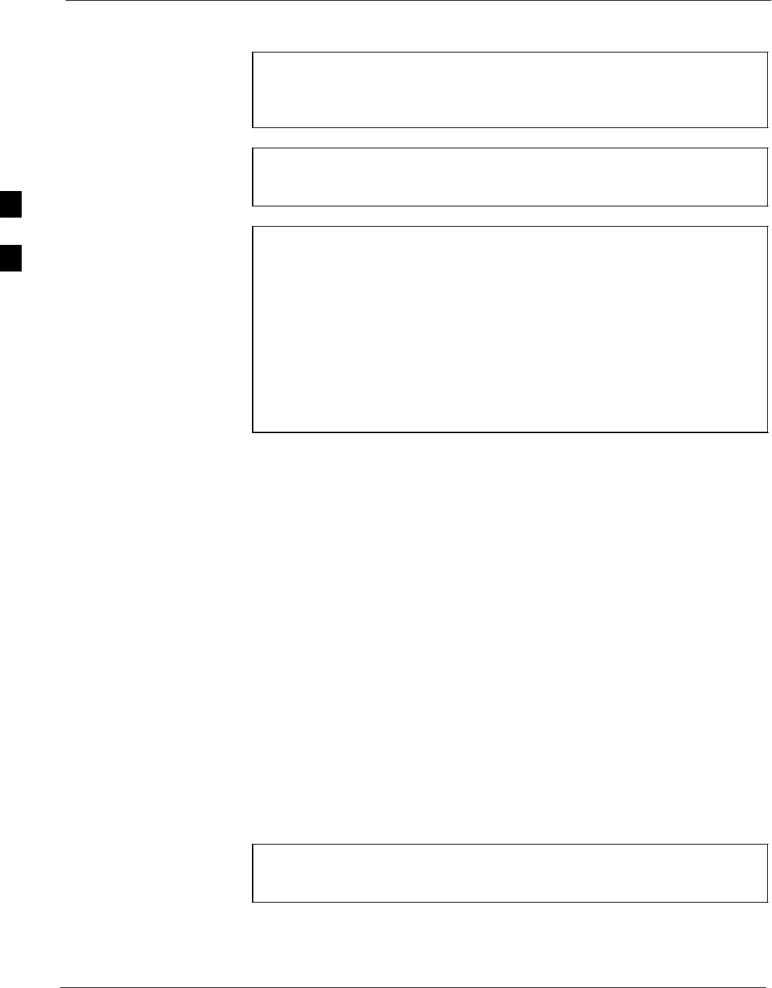
Bay Level Offset Calibration 68P09255A69-3
Aug 2002
1X SCt4812ET Lite BTS Optimization/ATP Software Release 2.16.1.x
PRELIMINARY
3-84
TX Calibration
WARNING Before installing any test equipment directly to any BTS TX
OUT connector, first verify no CDMA channels are keyed.
Failure to do so can result in serious personal injury and/or
equipment damage.
CAUTION Always wear an approved anti-static wrist strap while handling
any circuit card or module. If this is not done, there is a high
probability that the card or module could be damaged by ESD.
NOTE At new site installations, to facilitate the complete test of each
SCCP shelf (if the shelf is not already fully populated with BBX
boards), move BBX boards from shelves currently not under test
and install them into the empty BBX slots of the shelf currently
being tested to insure that all BBX TX paths are tested.
- This procedure can be bypassed on operational sites that are
due for periodic optimization.
- Prior to testing, view the CDF file to verify the correct
BBX slots are equipped. Edit the file as required to include
BBX slots not currently equipped (per Systems
Engineering documentation).
All Cal/Audit Procedure
The LMF All Cal/Audit procedure performs the combination of the TX
calibration, TX audit, and BLO download functions with one command.
Prerequisites
Before running this procedure, be sure that the following have been
done:
SThe card in slot CSM 1, GLIs, MCCs, and BBXs have correct code
and data loads.
SPrimary CSM and MGLI are INS_ACT (bright green).
SAll BBXs are OOS_RAM (yellow).
SIf running calibration or audit using a test pattern other than Pilot,
MCCs are INS_ACT (bright green).
STest equipment and test cables are calibrated and connected for TX
calibration.
SLMF is logged into the BTS in the GUI environment.
NOTE Verify all BBX boards removed and repositioned have been
returned to their assigned shelves/slots. Any BBX boards moved
since they were downloaded will have to be downloaded again.
Follow the procedure in Table 3-40 to perform BLO calibration on the
TX paths, download BLO values to the BBXs, and perform TX path
audit in one operation.
3

Bay Level Offset Calibration68P09255A69-3
Aug 2002 1X SCt4812ET Lite BTS Optimization/ATP Software Release 2.16.1.x
PRELIMINARY
3-85
Table 3-40: All Cal/Audit Procedure
Step Action
1If it has not already been done, configure test equipment for TX calibration by following the
procedure in Table 3-38.
2Click on the BBX(s) to be calibrated.
3If the Test Pattern to be used is Standard, CDFPilot, or CDF, select at least one MCC (refer to “Test
Pattern Drop-down Pick List” under “TX Calibration and the LMF” in this section).
4 Click Tests in the BTS menu bar, and select TX > All Cal/Audit... from the pull-down menus.
- A CDMA Test Parameters window will appear.
5Select the appropriate carrier(s) and sector(s) (carrier-bts#-sector#-carrier#) from those displayed in the
Channels/Carrier pick list.
NOTE
To select multiple items, hold down the Shift or Ctrl key while clicking on pick list items to select
multiple carrier(s)-sector(s).
6Verify that the correct channel number for the selected carrier is shown in the Carrier # Channels
box.
- If it is not, obtain the latest bts-#.cdf and cbsc-#.cdf files from the CBSC.
NOTE
If necessary, the correct channel number may be manually entered into the Carrier # Channels box.
7If at least one MCC was selected in Step 3, select the appropriate transfer rate (1 = 9600, 3 = 9600 1X)
from the drop-down list in the Rate Set box.
NOTE
The rate selection of 3 is only available if 1X cards are selected for the test.
8 If Verify BLO is to be used during the calibration, leave the checkbox checked (default).
9If Single-Sided BLO is to be used during the calibration, click on the checkbox.
* IMPORTANT
Single-Sided BLO should only be used for primary BBXs. Do not check the box when calibrating the
redundant BBX.
10 In the Test Pattern box, select the test pattern to use for the calibration from the drop-down list (refer
to “Test Pattern Drop-down Pick List” under “TX Calibration and the LMF” in this section).
11 Click OK to display the status report window followed by a Directions pop-up window.
12 Follow cable connection directions as they are displayed.
- When the calibration process is completed, results will be displayed in the status report window.
13 Click OK to close the status report window.
3

Bay Level Offset Calibration 68P09255A69-3
Aug 2002
1X SCt4812ET Lite BTS Optimization/ATP Software Release 2.16.1.x
PRELIMINARY
3-86
TX Calibration Procedure
The LMF TX calibration procedure performs only the BLO calibration
on the TX paths. The BLO download and TX audit functions must be
performed separately when this method is chosen to perform calibration.
Prerequisites
Before running this test, be sure that the following have been done:
SThe card in slot CSM 1, GLIs, MCCs, and BBXs have correct code
and data loads.
SPrimary CSM and MGLI are INS_ACT (bright green).
SAll BBXs are OOS_RAM (yellow).
SIf running calibration or audit using a test pattern other than Pilot,
MCCs are INS_ACT (bright green).
STest equipment and test cables are calibrated and connected for TX
calibration.
SLMF is logged into the BTS in the GUI environment.
NOTE Verify all BBX boards removed and repositioned have been
returned to their assigned shelves/slots. Any BBX boards moved
since they were downloaded will have to be downloaded again.
Follow the procedure in Table 3-41 to perform BLO calibration on the
TX paths.
Table 3-41: TX Calibration Procedure
Step Action
1If it has not already been done, configure test equipment for TX calibration by following the
procedure in Table 3-38.
2Click on the BBX(s) to be calibrated.
3If the Test Pattern to be used is Standard, CDFPilot, or CDF, select at least one MCC (refer to “Test
Pattern Drop-down Pick List” under “TX Calibration and the LMF” in this section).
4 Click Tests in the BTS menu bar, and select TX > TX Calibration... from the pull-down menus.
- A CDMA Test Parameters window will appear.
5Select the appropriate carrier(s) and sector(s) (carrier-bts#-sector#-carrier#) from those displayed in the
Channels/Carrier pick list (press and hold the Shift or Ctrl keyboard key to select multiple items).
NOTE
To select multiple items, hold down the Shift or Ctrl key while clicking on pick list items to select
multiple carrier(s)-sector(s).
6Verify that the correct channel number for the selected carrier is shown in the Carrier # Channels
box.
- If it is not, obtain the latest bts-#.cdf and cbsc-#.cdf files from the CBSC.
NOTE
If necessary, the correct channel number may be manually entered into the Carrier # Channels box.
. . . continued on next page
3
Bay Level Offset Calibration68P09255A69-3
Aug 2002 1X SCt4812ET Lite BTS Optimization/ATP Software Release 2.16.1.x
PRELIMINARY
3-87
Table 3-41: TX Calibration Procedure
Step Action
7If at least one MCC was selected in Step 3, select the appropriate transfer rate (1 = 9600, 3 = 9600 1X)
from the drop-down list in the Rate Set box.
NOTE
The rate selection of 3 is only available if 1X cards are selected for the test.
8 If Verify BLO is to be used during the calibration, leave the checkbox checked (default).
9If Single-Sided BLO is to be used during the calibration, click on the checkbox.
NOTE
Single-Sided BLO should only be used for primary BBXs. Do not check the box when calibrating the
redundant BBX.
10 In the Test Pattern box, select the test pattern to use for the calibration from the drop-down list (refer
to “Test Pattern Drop-down Pick List” under “TX Calibration and the LMF” in this section).
11 Click OK to display the status report window followed by a Directions pop-up window.
12 Follow the cable connection directions as they are displayed.
- When the calibration process is completed, results will be displayed in the status report window.
13 Click OK to close the status report window.
Exception Handling
In the event of a failure, the calibration procedure displays a FAIL
message in the status report window and provides information in the
Description field.
Re-check the test setup and connection and re-run the calibration. If the
calibration fails again, note specifics about the failure, and refer to
Chapter 6, Troubleshooting.
Download BLO Procedure
After a successful TX path calibration, the BLO calibration file data
must be downloaded to the BBXs. In the download process, BLO data is
extracted from the CAL file for the BTS and downloaded to the selected
BBX devices.
Prerequisites
Ensure the following prerequisites have been met before proceeding.
SBBXs to receive the download are OOS_RAM (yellow).
STX calibration was successfully completed
After a TX calibration has been performed using the procedure in
Table 3-41, follow the steps in Table 3-42 to download the BLO data to
the BBXs.
3
Bay Level Offset Calibration 68P09255A69-3
Aug 2002
1X SCt4812ET Lite BTS Optimization/ATP Software Release 2.16.1.x
PRELIMINARY
3-88
Table 3-42: Download BLO
Step Action
1Select the BBX(s) to be downloaded.
2 Click Device in the BTS menu bar, and select Download > BLO from the pull-down menus.
- A status report window displays the result of the download.
NOTE
Selected device(s) do not change color when BLO is downloaded.
3 Click OK to close the status report window.
Calibration Audit Introduction
The BLO calibration audit procedure confirms the successful generation
and storage of the BLO calibration values. The calibration audit
procedure measures the path gain or loss of every BBX transmit path at
the site. In this test, actual system tolerances are used to determine the
success or failure of a test. The same external test equipment set-up
required for TX calibration is used for TX audit.
*RF path verification, BLO calibration, and BLO data
download to BBXs must have been successfully completed
prior to performing the calibration audit.
IMPORTANT
TX Path Audit
Perform the calibration audit of the TX paths of all equipped BBX slots,
per the steps in Table 3-43.
Before installing any test equipment directly to any TX
OUT connector, first verify there are no CDMA BBX
channels keyed. Failure to do so can result in serious
personal injury and/or equipment damage.
WARNING
If a successful All Cal/Audit was completed, this
procedure does not need to be performed, as BLO is
downloaded as part of the All Cal/Audit.
NOTE
TX Audit Test
The Tests menu item, TX Audit, performs the TX BLO Audit test for
BBXs. All measurements are made through the appropriate TX output
connector using the TX calibration setup.
3

Bay Level Offset Calibration68P09255A69-3
Aug 2002 1X SCt4812ET Lite BTS Optimization/ATP Software Release 2.16.1.x
PRELIMINARY
3-89
Prerequisites
Before running this test, the following should be done:
SThe card in slot CSM 1, GLIs, BBXs have correct code load.
SPrimary CSM and MGLI are INS_ACT (bright green).
SAll BBXs are OOS_RAM (yellow).
STest equipment and test cables are calibrated and connected for TX
BLO calibration.
SLMF is logged into the BTS.
After a TX calibration has been performed using the procedure in
Table 3-41, or if verification of BLO data in the CAL file is required,
follow the procedure in Table 3-43 to perform a BTS TX path audit.
Table 3-43: TX Path Audit
Step Action
1If it has not already been done, configure test equipment for TX path audit by following the procedure
in Table 3-38 (TX audit uses the same configuration as TX calibration).
2Select the BBX(s) to be audited.
3If the Test Pattern to be used is Standard, CDFPilot, or CDF, select at least one MCC (refer to “Test
Pattern Drop-down Pick List” under “TX Calibraton and the LMF” in this section).
4 Click Tests in the BTS menu bar, and select TX > TX Audit... from the pull-down menus.
- A CDMA Test Parameters window will appear.
5Select the appropriate carrier(s) (carrier-bts#-sector#-carrier#) from those displayed in the
Channels/Carrier pick list (press and hold the <Shift> or <Ctrl> key to select multiple items).
NOTE
To select multiple items, hold down the Shift or Ctrl key while clicking on pick list items to select
multiple carrier(s)-sector(s).
6Verify that the correct channel number for the selected carrier is shown in the Carrier # Channels
box.
- If it is not, obtain the latest bts-#.cdf and cbsc-#.cdf files from the CBSC.
NOTE
If necessary, the correct channel number may be manually entered into the Carrier # Channels box.
7If at least one MCC was selected in Step 3, select the appropriate transfer rate (1 = 9600, 3 = 9600 1X)
from the drop-down list in the Rate Set box.
NOTE
The rate selection of 3 is only available if 1X cards are selected for the test.
8In the Test Pattern box, select the test pattern to use for the calibration from the drop-down list (refer
to “Test Pattern Drop-down Pick List” under “TX Calibration and the LMF” in this section).
9 Click OK to display the status report window followed by a Directions pop-up window.
10 Follow the cable connection directions as they are displayed.
- When the calibration process is completed, results will be displayed in the status report window.
11 Click on the Save Results or Dismiss button, as desired, to close the status report window.
3
Bay Level Offset Calibration 68P09255A69-3
Aug 2002
1X SCt4812ET Lite BTS Optimization/ATP Software Release 2.16.1.x
PRELIMINARY
3-90
Exception Handling
In the event of a failure, the calibration procedure displays a FAIL
message in the status report window and provides information in the
Description field.
Re-check the test setup and connections and re-run the test. If the tests
fail again, note specifics about the failure, and refer to Chapter 6,
Troubleshooting.
Create CAL File
The LMF Create Cal File function gets the BLO data from BBXs and
creates/updates the CAL file for the BTS. If a CAL file does not exist a
new one is created. If a CAL file already exists it is updated. After a
BTS has been fully optimized a copy of the CAL file must exist so it can
be transferred to the CBSC. If TX calibration has been successfully
performed for all BBXs and BLO data has been downloaded, a CAL file
will exist. Note the following:
SThe Create Cal File function only applies to selected (highlighted)
BBXs.
CAUTION Editing the CAL file is not encouraged as this action can cause
interface problems between the BTS and the LMF. To manually
edit the CAL file you must first logout of the BTS. If you
manually edit the CAL file and then use the Create Cal File
function the edited information will be lost.
Prerequisites
Before running this procedure, the following should be done:
SLMF is logged into the BTS
SBBXs are OOS_RAM (yellow)
SBLO has been downloaded to the BBXs
Table 3-44: Create CAL File
Step Action
1Select the applicable BBXs.
- The CAL file will be updated for the selected BBXs only.
2Click on Device in the BTS menu bar, and select Create Cal File from the pull-down menu.
- A status report window will appear and display the results of the action.
3Click the OK button to close the status report window.
3

RFDS Set-up and Calibration68P09255A69-3
Aug 2002 1X SCt4812ET Lite BTS Optimization/ATP Software Release 2.16.1.x
PRELIMINARY
3-91
RFDS Set-up and Calibration
RFDS Description
The optional RFDS is used to perform RF tests of the site from the
CBSC or from the LMF. The RFDS contains the following FRUs:
SAntenna Select Unit (ASU)
SFixed Wireless Terminal Interface Card (FWTIC)
SSubscriber Unit Assembly (SUA)
For complete information regarding the RFDS, refer to the CDMA
CDMA RFDS Hardware Installation; 68P64113A93, CDMA RFDS
User’s Guide; 68P64114A51, and the LMF Help function on-line
documentation.
RFDS Parameters
The bts-#.cdf file includes RFDS parameter settings that must match the
installed RFDS equipment. The paragraphs below describe the editable
parameters and their defaults. Table 3-45 explains how to edit the
parameter settings.
SRfdsEquip - valid inputs are 0 through 2.
0 = (default) RFDS is not equipped
1 = Non-Cobra/Patzer box RFDS
2 = Cobra RFDS
STsuEquip - valid inputs are 0 or 1
0 = (default) TSU not equipped
1 = TSU is equipped in the system
SMC1....4 - valid inputs are 0 or 1
0 = (default) Not equipped
1 = Multicouplers equipped in RFDS system
(SC9600 internal RFDS only)
SAsu1/2Equip - valid inputs are 0 or 1
0 = (default) Not equipped
1 = Equipped
STestOrigDN - valid inputs are ’’’ (default) or a numerical string up to
15 characters. (This is the phone number the RFDS dials when
originating a call. A dummy number needs to be set up by the switch,
and is to be used in this field.)
NOTE Any text editor may be used to open the bts-#.cdf file to verify,
view, or modify data. Because the bts-#.cdf file is generated on
a Unix system, a more sophisticated editor, such as MicroSoft
WordPad, will display file content in a more easily-read format
than many simple text editors.
3

RFDS Set-up and Calibration 68P09255A69-3
Aug 2002
1X SCt4812ET Lite BTS Optimization/ATP Software Release 2.16.1.x
PRELIMINARY
3-92
Checking and Setting RFDS Parameters
Follow the procedure in Table 3-45 to review and/or edit RFDS
parameters.
Table 3-45: RFDS Parameter Settings
Step Action
NOTE
Log out of the BTS prior to perform this procedure.
1Using a text editor, verify the following fields are set correctly in the bts-#.cdf file:
EXAMPLE:
Asu1Equip = 1
Asu2Equip = 0 (1 if system is non-duplexed)
Mc1Equip = 0
Mc2Equip = 0
Mc3Equip = 0
Mc4Equip = 0
RfdsEquip = 2
TestOrigDN = ’123456789’
TsuEquip = 1
NOTE
The above is an example of entries extracted from the bts-#.cdf file that should have been generated
by the OMC-R and copied to the LMF. These fields will have been set by the OMC-R if the
RFDSPARM database is modified for the RFDS.
2Save changes and/or quit the editor.
3Log into the BTS using an LMF GUI session(refer to Table 3-11).
4 If no changes were made to the bts-#.cdf file fields listed in step 1, proceed to Step 7. If changes were
made, continue with Step 5.
5NOTE
To make certain the complete data download is accepted, the MGLI should be OOS_RAM (yellow)
when RFDS parameter settings are downloaded.
When changes are made to RFDS parameters in the bts-#.cdf file, data must be downloaded to the
MGLI by performing the following:
5a - To be sure it does not take control when the MGLI is disabled, manually disable the redundant
GLI card by unseating it from the backplane connectors and sliding it partially out of the shelf
slot.
5b - Click on the MGLI.
5c - Click on Device in the BTS menu bar, and select Disable from the pull-down menu.
-- A status report window shows the status of the operation.
5d - When the operation is complete, click OK to close the status report window.
5e - Click on the MGLI (now OOS_RAM (yellow)).
5f - Click on Device in the BTS menu bar, and select Download > Data from the pull-down menus
(selected devices do not change color when data is downloaded).
-- A status report window shows the status of the download.
. . . continued on next page
3
RFDS Set-up and Calibration68P09255A69-3
Aug 2002 1X SCt4812ET Lite BTS Optimization/ATP Software Release 2.16.1.x
PRELIMINARY
3-93
Table 3-45: RFDS Parameter Settings
Step Action
5g - Click OK to close the status report window.
5h - Click on the MGLI.
5i - Click on Device in the BTS menu bar, and select Enable from the pull-down menu.
-- A status report window shows the status of the operation.
5j - When the operation is complete, click OK to close the status report window.
! CAUTION
When the MGLI changes to INS_ACT, data will automatically be downloaded to the RFDS. During
this process, the RFDS LED will slowly begin flashing red and green for approximately 2-3 minutes.
DO NOT attempt to perform any functions with the RFDS until the LED remains steady green.
5k - Re-seat the redundant GLI card into the backplane connectors and lock it in place with the ejector
tabs.
5l - Once the redundant GLI initializes, download data to it by selecting the card and, in the BTS
menu bar, clicking Device and selecting Download > Data from the pull-down menus.
6Any MCCs that were INS_ACT when the MGLI was disabled must be disabled, downloaded with
data, and re-enabled as follows:
6a - Select the devices to be reset by clicking on them or using Select from the BTS menu bar and
clicking on MCCs in the pull-down menu.
6b - In the BTS menu bar, click on Device and select Disable from the pull-down menu.
-- A status report window shows the status of the operation.
6c - Click OK to close the status report window.
6d - Repeat Step 6a to select the MCCs.
6e - Click on Device in the BTS menu bar and select Download > Data from the pull-down menu.
(Selected devices do not change colot when data is downoaded.)
- A status report window shows the status of the download.
6f - Click on OK to close the status report window.
6g - When data download is complete, enable the MCCs by following the procedure in Table 3-22.
7Click on the RFDS tab.
8Status the RFDS TSU by performing the following:
8a - Click on the SUA to select it.
8b - Click on TSU in the BTS menu bar, and select Status TSU from the pull-down menu.
-- A status report shows the software version number for the TSIC and SUA.
. . . continued on next page
3
RFDS Set-up and Calibration 68P09255A69-3
Aug 2002
1X SCt4812ET Lite BTS Optimization/ATP Software Release 2.16.1.x
PRELIMINARY
3-94
Table 3-45: RFDS Parameter Settings
Step Action
8c - Click OK to close the status report window.
NOTE
If the LMF displays an error message, check the following:
SEnsure AMR cable is correctly connected from the BTS to the RFDS.
SVerify RFDS has power.
SVerify RFDS status LED is green.
SVerify entries in RFDS fields of the bts-#.cdf file are correct (refer to step 1).
SStatus the MGLI and ensure it is communicating (by Ethernet) with the LMF, and is in the proper
state (INS_ACT (bright green)).
RFDS TSU NAM Programming
The Number Assignment Module (NAM) information needs to be
programmed into the TSU before it can receive and process test calls, or
be used for any type of RFDS test. The RFDS TSU NAM must be
programmed with the appropriate system parameters and phone number
during hardware installation. The TSU phone and TSU MSI must be
recorded for each BTS used for OMC-R RFDS software configuration.
NOTE The user will only need to program the NAM for the initial
installation of the RFDS.
3
RFDS Set-up and Calibration68P09255A69-3
Aug 2002 1X SCt4812ET Lite BTS Optimization/ATP Software Release 2.16.1.x
PRELIMINARY
3-95
Explanation of Parameters Used When Programming the TSU NAM
Table 3-46 defines the parameters used when editing the tsu.nam file.
Table 3-46: Definition of Parameters
Access Overload Code
Slot Index
System ID
Network ID
These parameters are obtained from the switch.
Primary Channel A
Primary Channel B
Secondary Channel A
Secondary Channel B
These parameters are the channels which are to be used in operation
of the system.
Lock Code
Security Code
Service Level
Station Class Mark
Do NOT change.
IMSI MCC
IMSI 11 12 These fields are obtained at the OMC using the following command:
OMC000>disp bts-# imsi
If the fields are blank, replace the IMSI fields in the NAM file to 0,
otherwise use the values displayed by the OMC.
MIN Phone Number These fields are the phone number assigned to the mobile. The ESN
and MIN must be entered into the switch as well.
NOTE
This field is different from the TODN field in the bts-#.cdf file. The
MIN is the phone number of the RFDS subscriber, and the TODN is
the number the subscriber calls.
3

RFDS Set-up and Calibration 68P09255A69-3
Aug 2002
1X SCt4812ET Lite BTS Optimization/ATP Software Release 2.16.1.x
PRELIMINARY
3-96
Valid NAM Ranges
Table 3-47 provides the valid NAM field ranges. If any of the fields are
missing or out-of-range, the RFDS will error out.
Table 3-47: Valid NAM Field Ranges
Valid Range
NAM Field Name Minimum Maximum
Access Overload Code 0 15
Slot Index 0 7
System ID 0 32767
Network ID 0 32767
Primary Channel A 25 1175
Primary Channel B 25 1175
Secondary Channel A 25 1175
Secondary Channel B 25 1175
Lock Code 0 999
Security Code 0 999999
Service Level N/A N/A
Station Class Mark 0 255
IMSI 11 12 0 99
IMSI MCC 0 999
MIN Phone Number N/A N/A
3

RFDS Set-up and Calibration68P09255A69-3
Aug 2002 1X SCt4812ET Lite BTS Optimization/ATP Software Release 2.16.1.x
PRELIMINARY
3-97
Set Antenna Map Data
The antenna map data must be entered manually if an RFDS is installed.
Antenna map data does not need to be entered if an RFDS is not
installed. The antenna map data is only used for RFDS tests and is
required if an RFDS is installed.
Prerequisite
SLMF is logged into the BTS
Follow the procedure in Table 3-48 to set antenna map data for the
RFDS.
Table 3-48: Set Antenna Map Data
Step Action
1Click on Util in the BTS menu bar, and select Edit > Antenna Map... from the pull-down menus.
-A tabbed data entry pop-up window will appear.
2In the data entry pop-up window, click on the TX Antenna Map or RX Antenna Map tab to select
the antenna map to be edited.
3Locate the carrier and sector number for which data is to be entered or edited, and click in the column
where entry or editing is needed.
4Enter/edit Antenna # and Antenna Label column data as needed for each carrier.
NOTE
Refer to the CDMA Help > Utility Menu > Edit-Antenna Map... section of LMF Help function
on-line documentation for antenna map examples.
5For each tab with changes, click on the Save button to save displayed values.
6Click on the Dismiss button to close the window.
NOTE
SValues entered or changed after the Save button was used will be lost when the window is
dismissed.
SEntered values will be used by the LMF as soon as they are saved. It is not necessary to log out and
log back into the LMF for changes to take effect.
3

RFDS Set-up and Calibration 68P09255A69-3
Aug 2002
1X SCt4812ET Lite BTS Optimization/ATP Software Release 2.16.1.x
PRELIMINARY
3-98
Set RFDS Configuration Data
If an RFDS is installed, the RFDS configuration data must be manually
entered.
Prerequisite
SLMF is logged into the BTS
NOTE The entered antenna# index numbers must correspond to the
antenna# index numbers used in the antenna maps.
Follow the procedure in Table 3-49 to set RFDS configuration data.
Table 3-49: Set RFDS Configuration Data
Step Action
1Click on Util in the BTS menu bar, and select Edit > RFDS Configuration... from the pull-down
menus.
-A tabbed data entry pop-up window will appear.
2In the data entry pop-up window, click on the TX RFDS Configuration or RX RFDS Configuration
tab, as required.
3To add a new antenna number, perform the following:
3a - Click on the Add Row button.
3b - Click in the Antenna #, Cal Antenna, Scap Antenna, or Populate [Y/N] columns, as required.
3c - Enter the desired data.
4To edit existing values click in the data box to be changed and change the value.
NOTE
Refer to the CDMA Help > Utility Menu > Edit-RFDS Configuration... section of LMF Help
function on-line documentation for RFDS configuration data examples.
5To delete a row, click on the row and then click on the Delete Row button.
6For each tab with changes, click on the Save button to save displayed values.
7Click on the Dismiss button to close the window.
NOTE
SValues entered or changed after the Save button was used will be lost when the window is
dismissed.
SEntered values will be used by the LMF as soon as they are saved. It is not necessary to log out and
log back into the LMF for changes to take effect.
3
RFDS Set-up and Calibration68P09255A69-3
Aug 2002 1X SCt4812ET Lite BTS Optimization/ATP Software Release 2.16.1.x
PRELIMINARY
3-99
RFDS Calibration
The RFDS Calibration option is used to calibrate the RFDS TX and RX
paths.
TX Path Calibration - For a TX antenna path calibration the BTS
XCVR is keyed at a pre-determined power level and the BTS power
output level is measured by the RFDS. The power level is then measured
at the TX antenna directional coupler by the power measuring test
equipment item being used (power meter or analyzer). The difference
(offset) between the power level at the RFDS and the power level at the
TX antenna directional coupler is used as the TX RFDS calibration
offset value.
RX Path Calibration - For an RX antenna path calibration the RFDS is
keyed at a pre-determined power level and the power input level is
measured by the BTS BBX. A CDMA signal at the same power level
measured by the BTS BBX is then injected at the RX antenna directional
coupler by the communications system analyzer. The difference (offset)
between the RFDS-keyed power level and power level measured at the
BTS BBX is the RFDS RX calibration offset value.
RFDS calibration and the CAL file - The TX and RX RFDS
calibration offset values are written to the CAL file in the slot[385]
Block.
TSIC channel frequency - For each RFDS TSIC, the channel
frequency is determined at the lower third and upper third of the
appropriate band using the frequencies listed in Table 3-50.
Table 3-50: RFDS TSIC Calibration Channel Frequencies
System Channel Calibration Points
800 MHz (A and B) 341 and 682
1.9 GHz 408 and 791
Before installing any test equipment directly to any TX
OUT connector, verify that there are no CDMA channels
keyed. Failure to do so can result in serious personal injury
and/or equipment damage.
WARNING
3

RFDS Set-up and Calibration 68P09255A69-3
Aug 2002
1X SCt4812ET Lite BTS Optimization/ATP Software Release 2.16.1.x
PRELIMINARY
3-100
RFDS Calibration Procedure
Prerequisites
STest equipment has been selected.
STest equipment and test cables have been calibrated.
STX calibration has been performed and BLO data has been
downloaded to the BBXs.
STest equipment and test cables are connected for TX calibration.
SAntenna map data has been entered for the site.
SBBXs are OOS-RAM.
Follow the procedure in Table 3-51 to perform RFDS calibration.
Table 3-51: RFDS Calibration
Step Action
1In the LMF, select the BTS tab.
2If the BTS Control button is not selected (no black dot showing), click on the B button in the BTS
menu bar to select it.
3Select the BBX(s) assigned to the carrier(s) and sector(s) which will be used in RFDS calibration
(refer to Table 1-5 for BBX carrier and sector assignments).
4Click on RFDS in the BTS menu bar, and select RFDS Calibration... from the pull-down menu.
- An RFDS Calibration set-up window will be displayed.
5In the Tests to Perform box, select TX Calibration or RX Calibration, as required
6Enter the appropriate channel number(s) (refer to Table 3-50) in the Channel Field box.
STo enter more than one channel number, use the following methods:
- Separate non-sequential channel numbers with a comma and no spaces;
for example: 247,585,742.
- Enter a range of sequential channels by typing the first and last channel numbers in the range
separated by a dash and no spaces;
for example: 385-395.
7If the frame is equipped with TX combiners, click in the Has Combiners checkbox.
8Select the appropriate carrier(s) and sector(s) from the Carriers pick list (hold down the Shift or Ctrl
key while clicking on pick list items to select multiple carrier(s)-sector(s)).
9Select the appropriate RX branch (Both, Main, or Diversity) in the drop-down list if performing RX
calibration.
10 Click on the OK button.
- A status report window is displayed, followed by a Directions pop-up window.
11 Follow the cable connection directions as they are displayed.
12 When the test is completed, test results are displayed in the status report window.
13 Click on the OK button to close the status report window.
14 Click on the Frame tab.
15 Select the MGLI by clicking on it.
16 Download updated RFDS offset data to the MGLI (see Step 5 in Table 3-45).
3

RFDS Set-up and Calibration68P09255A69-3
Aug 2002 1X SCt4812ET Lite BTS Optimization/ATP Software Release 2.16.1.x
PRELIMINARY
3-101
Program TSU NAM
The NAM must be programmed before it can receive and process test
calls, or be used for any type of RFDS test.
Prerequisites
SMGLI is INS_ACT (bright green).
SSUA is powered up and has a code load.
Follow the procedure in Table 3-52 to program the TSU NAM.
Table 3-52: Program NAM Procedure
Step Action
1In the LMF, select the RFDS tab.
2Select the SUA by clicking on it.
3Click on TSU in the BTS menu bar, and select Program TSU NAM from the pull-down menu.
- A NAM programming window will appear.
4Enter the appropriate information in the boxes (see Table 3-46 and Table 3-47) .
5Click on the OK button to display the status report.
6Click on the OK button to close the status report window.
3

Alarms Testing 68P09255A69-3
Aug 2002
1X SCt4812ET Lite BTS Optimization/ATP Software Release 2.16.1.x
PRELIMINARY
3-102
Alarms Testing
Alarm Verification
Alarms testing should be performed at a convenient point in the
optimization/ATP process, since the LMF is necessary to ensure that the
SC4812ET Lite is generating the appropriate alarms.
The SC 4812ET Lite is capable of concurrently monitoring 10 customer
defined input signals and four customer defined outputs, which interface
to the 50-pair punchblock. All alarms are defaulted to “Not Equipped”
during ATP testing. Testing of these inputs is achieved by triggering the
alarms and monitoring the LMF for state-transition messages from the
MGLI.
Alarm Reporting Display
The Alarm Monitor window can be displayed to list alarms that occur
after the window is displayed. The Alarm Monitor window is accessed
from the BTS menu bar.
The following buttons are included in the Alarm Monitor window:
SThe Options button allows for a severity level (Warning, Minor,
Major, Critical, and Unknown) selection. The default is all levels.
To change the level of alarms reported click on the Options button
and highlight the desired alarm level(s). To select multiple levels press
the Ctrl key (for individual selections) or Shift key (for a range of
selections) while clicking on the desired levels.
SThe Pause button can be used to pause/stop the display of alarms.
When the Pause button is clicked the name of the button changes to
Continue. When the Continue button is click the display of alarms
will continue. Alarms that occur between the time the Pause button is
clicked and the Continue button is clicked will not be displayed.
SThe Clear button can be used to clear the Alarm Monitor display.
New alarms that occur after the Clear button is clicked will be
displayed.
SThe Dismiss button is used to dismiss/close the Alarm Monitor
display.
3

Alarms Testing68P09255A69-3
Aug 2002 1X SCt4812ET Lite BTS Optimization/ATP Software Release 2.16.1.x
PRELIMINARY
3-103
Alarm Testing Set-up
Prepare for any alarm testing by following the procedures in Table 3-53.
Table 3-53: Alarm Testing Preparation
Step Action
1If it has not already been done, refer to the procedure in Table 3-10 to connect the LMF computer
terminal to the frame LAN A connector.
2If it has not already been done, refer to Table 3-11 to start a GUI LMF session.
3Click on Util in the BTS menu bar, and select Alarm Monitor... from the pull-down menu.
- An Alarm Monitor window will open.
Heat Exchanger Alarm Test
Table 3-54 gives instructions on testing the Heat Exchanger alarm.
Table 3-54: Heat Exchanger Alarm
Step Action
1Set one of the two DC PDA heat exchanger circuit breakers to OFF. This will generate a heat
exchanger alarm. Be sure that the LMF reports the correct alarm condition.
2Alarm condition will be reported as BTS Relay #14, BTS Relay #15, BTS Relay #16, BTS Relay
#17, BTS Relay #18, with Contact Alarm Open*Clear*, respectively.
3Set the circuit breaker turned off in step 1 to ON. Ensure that the alarm conditions have cleared on
the LMF with Contact Alarm Closed*Clear* for each reported BTS relay.
NOTE
The heat exchanger will go through the start-up sequence.
Door Alarm
Table 3-55 gives instructions on testing the door alarms.
Table 3-55: ACLC and Power Entry Door Alarm
Step Action
1Close the ACLC and power entry compartment doors on the frame. Ensure that no alarms are reported
on the LMF.
2Individually open and then close the ACLC and power entry compartment door. Ensure that the LMF
reports an alarm when each door is opened.
3Alarm condition will be reported as BTS Relay #27 contact.
3
Alarms Testing 68P09255A69-3
Aug 2002
1X SCt4812ET Lite BTS Optimization/ATP Software Release 2.16.1.x
PRELIMINARY
3-104
AC Fail Alarm
Table 3-56 gives instructions on testing the AC Fail Alarm.
Table 3-56: AC Fail Alarm
Step Action
1NOTE
- Back-up batteries must be installed when performing this test.
- To prevent inadvertently shutting down the RF compartment electronics, the batteries should be
charged before performing this test.
Set the ACLC MAIN circuit breaker to OFF.
- The LMF should report an alarm for an AC Fail condition as BTS Relay #21, BTS Relay #23,
BTS Relay #24, and BTS Relay #29 contacts, respectively.
- On the MAP, the MAJOR ALARM (red), MINOR ALARM (amber), and RECTIFIER FAIL
(red) LEDs should light.
- On the rectifiers, the DC and PWR LEDs should light red.
2Set the ACLC MAIN circuit breaker to ON.
- On the LMF, the AC Fail alarm should clear.
- On the MAP, the MAJOR ALARM, MINOR ALARM, and RECTIFIER FAIL LEDs should
extinguish.
- On the rectifiers, the DC and PWR LEDs should change to green.
Minor Alarm
Table 3-57 gives instructions on performing a test to display a minor
alarm.
Table 3-57: Minor Alarm
Step Action
1Set the TCP switch on the MAP to OFF. This will generate a minor alarm.
- The LMF should report the minor alarm as BTS Relay #24 contacts.
- The TC DISABLE (red) and MINOR ALARM (amber) LEDs on the MAP should light.
2Set the TCP switch to ON.
- The alarm condition indications should clear.
Rectifier Alarms
The following series of tests are for single rectifier modules in a multiple
rectifier system. The systems include a three rectifier and a four rectifier
system.
3

Alarms Testing68P09255A69-3
Aug 2002 1X SCt4812ET Lite BTS Optimization/ATP Software Release 2.16.1.x
PRELIMINARY
3-105
Single Rectifier Failure (Three Rectifier System)
Table 3-58 gives instructions on testing single rectifier failure or minor
alarm in a three (3) rectifier system (single-carrier system). Procedures
in this test are for a frame configured for single carrier operation with
rectifiers installed in rectifier shelf positions 1, 2, and 3, from left to
right when facing the frame.
Table 3-58: Single Rectifier Fail or Minor Alarm, Single-Carrier System
Step Action
1! CAUTION
Only perform this test if the rectifier current load displayed on the AMP indicator on the MAP is
125 amps or less. Sufficient current capability to support a greater load may not be available when
one rectifier is removed from the bus.
On the ACLC, set the RECT. 2/4 circuit breaker to OFF.
- The DC and PWR LEDs should light red on the rectifier in shelf position 2.
- The MINOR ALARM (amber) and RECTIFIER FAIL (red) LEDs on the MAP should light.
- The LMF should report an alarm condition as BTS Relay #21 and BTS Relay #24 contacts,
respectively.
2Set the RECT. 2/4 circuit breaker on the ACLC to ON.
- All alarm indications should clear on the rectifier, MAP, and LMF.
Multiple Rectifier Failure (Three Rectifier System)
Table 3-59 gives instructions on testing multiple rectifier failure or major
alarm in a three (3) rectifier system (single-carrier system). Procedures
in this test are for a frame configured for single carrier operation with
rectifiers installed in rectifier shelf positions 1, 2, and 3, from left to
right when facing the frame.
Table 3-59: Multiple Rectifier Failure or Major Alarm, Single-Carrier System
Step Action
1! CAUTION
Only perform this test if the rectifier current load displayed on the AMP indicator on the MAP is 65
amps or less. Sufficient current capability to support a greater load may not be available when two
rectifiers are removed from the bus.
On the ACLC, set the RECT. 1/3 circuit breaker to OFF.
- The DC and PWR LEDs should light red on the rectifiers in shelf positions 1 and 3.
- The MAJOR ALARM (red), MINOR ALARM (amber), and RECTIFIER FAIL (red) LEDs on
the MAP should light.
- The LMF should report an alarm condition as BTS Relay #21, BTS Relay #24, and BTS Relay
#29 contacts, respectively.
2Set the RECT. 1/3 circuit breaker on the ACLC to ON.
- All alarm indications should clear on the rectifiers, MAP, and LMF.
3

Alarms Testing 68P09255A69-3
Aug 2002
1X SCt4812ET Lite BTS Optimization/ATP Software Release 2.16.1.x
PRELIMINARY
3-106
Single Rectifier Failure
(Four Rectifier System)
Table 3-60 gives instructions on testing single rectifier failure or minor
alarm in a four (4) rectifier system (two-carrier system).
Table 3-60: Single Rectifier Fail or Minor Alarm, Two-Carrier System
Step Action
1! CAUTION
Only perform this test if the rectifier current load displayed on the AMP indicator on the MAP is
125 amps or less. Sufficient current capability to support a greater load may not be available when
two rectifiers are removed from the bus in the following steps.
Unseat the rectifier in shelf position 4 from its connection at the rear of the shelf, but do not
completely remove it from the shelf.
- The rectifier 4 DC and PWR LEDs may light red momentarily and extinguish. There should be
no other indications on the frame or LMF.
2On the ACLC, set the RECT. 2/4 circuit breaker to OFF.
- The rectifier 2 DC and PWR LEDs should light red.
- The MINOR ALARM (amber) and RECTIFIER FAIL (red) LEDs on the MAP should light.
- The LMF should report an alarm condition as BTS Relay #21 and BTS Relay #24 contacts,
respectively.
3Re-seat the rectifier in shelf position 4 into its connection at the rear of the shelf.
4 On the ACLC, set the RECT. 2/4 circuit breaker to ON.
- The rectifier DC and PWR LEDs should light green.
- All alarm indications should clear on the rectifiers, MAP, and LMF.
3
Alarms Testing68P09255A69-3
Aug 2002 1X SCt4812ET Lite BTS Optimization/ATP Software Release 2.16.1.x
PRELIMINARY
3-107
Multiple Rectifier Failure (Four Rectifier System)
Table 3-61 gives instructions on testing multiple rectifier failure or major
alarm in a four (4) rectifier system (two-carrier system).
Table 3-61: Multiple Rectifier Failure or Major Alarm, Two-Carrier System
Step Action
1! CAUTION
Only perform this test if the rectifier current load displayed on the AMP indicator on the MAP is
125 amps or less. Sufficient current capability to support a greater load may not be available when
two rectifiers are removed from the bus.
On the ACLC, set the RECT. 2/4 circuit breaker to OFF.
- The DC and PWR LEDs should light red on the rectifiers in shelf positions 2 and 4.
- The MAJOR ALARM (red), MINOR ALARM (amber), and RECTIFIER FAIL (red) LEDs on
the MAP should light.
- The LMF should report an alarm condition as BTS Relay #21, BTS Relay #24, and BTS Relay
#29 contacts, respectively.
2Set the RECT. 2/4 circuit breaker on the ACLC to ON.
- All alarm indications should clear on the rectifiers, MAP, and LMF.
3

Alarms Testing 68P09255A69-3
Aug 2002
1X SCt4812ET Lite BTS Optimization/ATP Software Release 2.16.1.x
PRELIMINARY
3-108
Battery Over Temperature Alarm (Optional)
CAUTION Use special care to avoid damaging insulation on cables, or
damaging battery cases when using a heat gun.
Table 3-62 gives instructions on testing the battery over-temperature
alarm system.
Table 3-62: Battery Over-Temperature Alarm
Step Action
1Use a low-powered heat gun to gently heat the battery over-temperature sensor (see location in
Figure 3-24).
! CAUTION
To avoid damaging the cable insulation, do not hold the hot air gun closer than three (3) inches from
the sensor.
2NOTE
When the over-temperature alarm point is reached, an audible click will sound as DC PDA relay K1
contacts engage and relay K2 contacts disengage (make-before-break operation).
When the sensor is heated to approximately 51° C, a battery over-temperature alarm is generated with
the following indications.
- On the MAP, the CHARGE DISABLE LED (red) should light and the MAIN CONN. ENABLE
LED (green) should extinguish.
- The LMF should display an alarm condition as BTS Relay #22 contacts.
3Switch the hot air gun to cool. Cool the sensor until the K1 and K2 contacts return to normal position
(K1 open and K2 closed). The following indications that alarms have cleared should occur:
- On the MAP, the CHARGE DISABLE LED (red) should extinguish and the MAIN CONN.
ENABLE (green) LED should light.
- The alarm reported on LMF will clear
3
Alarms Testing68P09255A69-3
Aug 2002 1X SCt4812ET Lite BTS Optimization/ATP Software Release 2.16.1.x
PRELIMINARY
3-109
Figure 3-24: Battery Over-Temperature Sensor
Bus Bar
6 AWG Cables
Battery Overtemp Sensor
Negative Temperature Compensation Sensor
SC4812ETL0014-1
3
Alarms Testing 68P09255A69-3
Aug 2002
1X SCt4812ET Lite BTS Optimization/ATP Software Release 2.16.1.x
PRELIMINARY
3-110
Rectifier Over Temperature Alarm
Table 3-63 gives instructions on testing the rectifier over-temperature
alarm system.
CAUTION Do not attempt to remove the MAP from the front of the frame
to perform the following procedure, even if the frame is equipped
with a MAP cable tray. MAP removal from the front requires
complete site shut-down to avoid accidently shorting 27 Vdc to
ground during the removal process.
Table 3-63: Rectifier Over-Temperature Alarm
Step Action
1Remove the 14 tamper-resistant TORX fasteners securing the rear access panel to the rear of the
frame (Figure 2-1), and remove the rear access panel.
NOTE
Panel fastener type can be either T-27 button head or T-30 pan head.
2Looking up through the frame rear access opening, locate the rear of the MAP.
3Remove the jumper plug from connector J8 on the rear panel of the MAP (Figure 3-25). The
following conditions should occur:
- Contacts on K1 and K2 change states (K1 now closed and K2 open).
- The LMF reports an alarm condition as BTS Relay #26 contacts.
4Reinstall the jumper plug in connector J8, and verify that all alarm conditions have cleared.
5Reinstall the frame rear access panel, securing it with the 14 tamper-resistant TORX fasteners
removed in step 1.
Figure 3-25: MAP Connector J8 (Rear of MAP)
J4 J5 J1
J12
J3 J8 J9 J7
J2
CONNECTOR J8
SC4812ETL0021-2
Before Leaving the Site
If no further operations are required after performing the alarm tests,
complete the requirements in Table 5-8 before leaving the site.
3