Nokia Solutions and Networks T5CS1 Cellular CDMA Base Station User Manual IHET5SC1 GLI3 3 of 4
Nokia Solutions and Networks Cellular CDMA Base Station IHET5SC1 GLI3 3 of 4
Contents
IHET5SC1 GLI3 User Manual 3 of 4

Aug 2002 1X SCt4812ET Lite BTS Optimization/ATP Software Release 2.16.1.x
PRELIMINARY
4-1
Chapter 4
Automated Acceptance Test
Procedures
4

Automated Acceptance Test Procedure - Introduction 68P09255A69-3
Aug 2002
1X SCt4812ET Lite BTS Optimization/ATP Software Release 2.16.1.x
PRELIMINARY
4-2
Automated Acceptance Test Procedure - Introduction
Introduction
General
The Acceptance Test Procedures (ATP) allow Cellular Field Engineers
(CFEs) to run automated acceptance tests on all BTS subsystem devices
equipped in the CDF using the LMF and the test equipment it supports.
Test Reports
The CFE can choose to save the results of ATP tests to a report file from
which ATP reports are generated for later printing. See the Generating an
ATP Report section in this chapter.
Test Equipment Selection
Because test equipment functions during acceptance testing are
controlled by the LMF through the GPIB, only the test equipment
models supported by the LMF can be used.
NOTE 1. Before using the LMF, read the Developer Release Notes
section in the LMF Help function on-line documentation for
any applicable information.
2. The ATP test is to be performed on out-of-service sectors
only.
3. DO NOT substitute test equipment with other models not
supported by the LMF.
Test Equipment Set Calibration
Refer to Chapter 3 for detailed interconnection information needed for
calibrating equipment, cables, and other test equipment set components.
Reduced ATP
NOTE Equipment has been factory-tested for FCC compliance. If
license-governing bodies require documentation supporting BTS
site compliance with regulations, a full ATP may be necessary.
Perform the Reduced ATP only if reports for the specific BTS
site are NOT required.
After downloading the proper operational software to the BTS, the CFE
must perform these procedures (minimum recommendation):
1. Verify the TX/RX paths by performing TX Calibration, TX Audit,
and FER tests.
2. Retrieve Calibration Data required for normal site operation.
Should failures occur while performing the specified tests, refer to the
Basic Troubleshooting section of this manual for help in determining the
failure point. Once the point of failure has been identified and corrected,
refer to the BTS Optimization and ATP Test Matrix (Table B-1) in the
FRU Optimization/ATP Test Matrix section of Appendix B to determine
the applicable test that must be performed.
4

Automated Acceptance Test Procedure - Introduction68P09255A69-3
Aug 2002 1X SCt4812ET Lite BTS Optimization/ATP Software Release 2.16.1.x
PRELIMINARY
4-3
In the unlikely event that the BTS passes these tests but has a forward
link problem during normal operation, the CFE should then perform the
additional TX tests for troubleshooting: TX spectral mask, TX rho, and
TX code domain.
ATP Test Options
ATP tests can be run individually or as one of the following groups:
SAll TX: TX tests verify the performance of the BTS transmit
elements. These include the GLI, MCC, BBX, trunking modules, the
LPAs, and passive components including splitters, combiners,
bandpass filter(s), and RF cables.
SAll RX: The RX test verifies the performance of the BTS receive
elements. These include the MPC, EMPC (for companion frames),
BBX, MCC, GLI modules, and the passive components including RX
filters and RF cables.
SAll TX/RX: Executes all TX and RX tests.
SFull Optimization: Executes the TX calibration, downloads BLO,
and executes the TX audit before running all TX and RX tests.
ATP Prerequisites
Before attempting to run any ATP tests, be sure the following have been
completed:
SBTS has been optimized (BBXs calibrated and BLOs downloaded)
(Chapter 3)
SThe carrier(s) and/or sector(s) to be tested have been taken out of
service at the CBSC.
SLMF is logged into the BTS.
SCSMs, GLIs, BBXs, MCCs and TSU (if the RFDS is installed) have
correct code and data loads.
SPrimary CSM and GLI are INS_ACT (bright green).
SMCCs are INS_ACT (bright green).
SNo BBXs are keyed (transmitting).
SBBXs are OOS_RAM (yellow).
STest cables are calibrated.
STest equipment has been selected, warmed up 60 minutes, and
calibrated.
SGPIB is on.
SBTS transmit connectors are properly terminated for the test(s) to be
performed.
4

Automated Acceptance Test Procedure - Introduction 68P09255A69-3
Aug 2002
1X SCt4812ET Lite BTS Optimization/ATP Software Release 2.16.1.x
PRELIMINARY
4-4
WARNING 1. All transmit connectors must be properly terminated for all
ATP tests.
2. Before the FER is run, be sure that one of the following is
done:
- All transmitter connectors are properly terminated
OR
- All LPAs are turned OFF (circuit breakers pulled)
Failure to observe these warnings may result in bodily injury or
equipment damage.
TX/RX Antenna Connections
Starter (Stand-alone) Frames
Refer to Figure 1-7 or Figure 1-8 for identification of starter frame
transmit and receive antenna connections where measurements are to be
taken. All ATP test equipment connections for starter frames are made at
the ANTENNAS connectors on the RF interface panel.
Companion Frames
TX ATP Antenna Connections - Each companion frame at a site
connects independently to transmit antennas. Test equipment
connections for TX ATPs on each companion frame are made at the
ANTENNAS connectors as on starter frames. Companion frame
ANTENNAS connectors are shown in Figure 1-9 and Figure 1-10.
Antenna Connections for RX main ATP - Each companion frame at a
site uses independent receive antennas for main RX signals. The main
RX signals are either routed through TRDC RX ANTENNAS
connectors (Figure 1-10) or duplexed with TX signals through the single
DRDC ANTENNAS connectors (Figure 1-9).
Antenna Connections for RX diversity ATP - Companion frame
diversity RX signals are obtained from the RX main antenna of the
collocated companion frame. The main RX signals are sent from the
collocated companion frame through inter-frame diversity RX cables to
the RX EXPANSION 1B, 2B, or 3B connectors of the frame where they
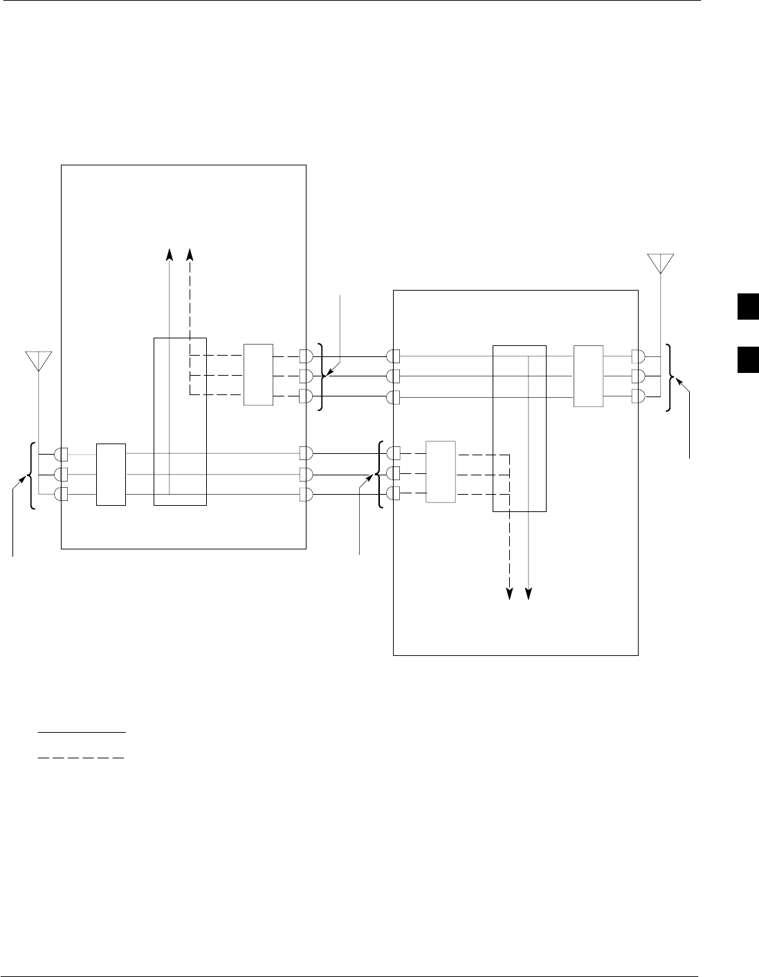
are used for diversity RX (refer to Figure 4-1). Diversity RX ATP test
equipment connections are made at one of two different locations
depending on whether or not the companion frame under test is
connected to a collocated companion frame. Connection points for each
situation are as follows:
SConnected companion frames: When inter-frame diversity RX
cables are connected, connect test equipment for diversity RX ATP at
the ANTENNAS connectors of the collocated companion frame as
shown in Figure 4-1 and listed in Table 4-1. Be sure MPC is selected
before logging the LMF into the frame or FER will fail.
4
Automated Acceptance Test Procedure - Introduction68P09255A69-3
Aug 2002 1X SCt4812ET Lite BTS Optimization/ATP Software Release 2.16.1.x
PRELIMINARY
4-5
SDisconnected companion frames: When inter-frame diversity RX
cables are disconnected, connect test equipment for diversity RX ATP
at the RX EXPANSION connectors 1B, 2B, or 3B on the frame under
test. Refer to Figure 4-1 and Table 4-2. Be sure EMPC is selected
before logging the LMF into the frame or FER will fail.
Figure 4-1: SC4812ET Lite Companion Frame Diversity RX Simplified Interconnection Diagram
MPC
1A
2A
3A
CIO
EMPC
INTER-FRAME
DIVERSITY RX
CABLES
1A
2A
3A
RX MAIN
(3 SECTORS) RX DIVERSITY
(3 SECTORS)
RX MAIN
(3)
TO
BBXS
ANTENNAS
CONNECTORS
(TRDC/DRDC)
RX EXPANSION
CONNECTORS
SC4812ET LITE COMPANION FRAME 1
MPC
1A
2A
3A
CIO
EMPC
1A
2A
3A
RX MAIN
(3)
TO
BBXS
SC4812ET LITE COMPANION FRAME 2
RX EXPANSION
CONNECTORS
ANTENNAS
CONNECTORS
(TRDC/DRDC)
SC4812ETL0045-1
SIGNALS: RX MAIN
RX DIVERSITY
NOTE: ANTENNAS connectors represent TRDC/DRDC portion of receive path.
RX DIVERSITY ATP CONNECTION POINTS:
1: For Companion Frame 1 when inter-frame diversity
RX cables are connected.
2: For Companion Frame 1 when inter-frame diversity
RX cables are disconnected.
3: For Companion Frame 2 when inter-frame diversity
RX cables are connected.
4: For Companion Frame 2 when inter-frame diversity
RX cables are disconnected.
1
2
34
RX EXPANSION
CONNECTORS
RX EXPANSION
CONNECTORS
3B
2B
1B
3B
2B
1B
RX MAIN
(3 SECTORS)
RX DIVERSITY
(3 SECTORS)
4

Automated Acceptance Test Procedure - Introduction 68P09255A69-3
Aug 2002
1X SCt4812ET Lite BTS Optimization/ATP Software Release 2.16.1.x
PRELIMINARY
4-6
Table 4-1: To Perform Companion Frame Diversity RX FER,
Inter-frame RX Cables Connected
(Set Multi-Channel Preselector to MPC)
On Connect RX Test Cable to
Collocated Companion Frame
Carrier Sector
Collocated Companion Frame
RX or Duplexed TX/RX
ANTENNAS Connector
1 1A
12 2A
3 3A
1 1A
22 2A
3 3A
Table 4-2: To Perform Companion Frame Diversity RX FER,
Inter-frame RX Cables Disconnected
(Set Multi-Channel Preselector to EMPC)
On Connect RX Test Cable to
Carrier Sector Frame Under Test
RX EXPANSION Connector
1 1B
12 2B
3 3B
1 1B
22 2B
3 3B
4

Acceptance Tests - Test Set-up68P09255A69-3
Aug 2002 1X SCt4812ET Lite BTS Optimization/ATP Software Release 2.16.1.x
PRELIMINARY
4-7
Acceptance Tests - Test Set-up
Required Test Equipment
The following test equipment is required:
SLMF
SPower meter (used with HP8921A/600 and Advantest R3465)
SCommunications system analyzer
SSignal generator for FER testing (required for all communications
system analyzers for 1X FER)
WARNING -Before installing any test equipment directly to any BTS
TX OUT connector, verify that there are no CDMA
channels keyed.
- At active sites, have the OMCR/CBSC place the carrier
assigned to the LPAs under test OOS. Failure to do so can
result in serious personal injury and/or equipment damage.
NOTE The test equipment must be re-calibrated before using it to
perform the TX Acceptance Tests.
Acceptance Test Equipment Set Up
All ATP testing - Follow the steps in Table 4-3 to set up test equipment
for all tests.
Table 4-3: Set Up Test Equipment - TX Output Verify/Control Tests
Step Action
1If it has not already been done, interface the LMF computer to the BTS (refer to Table 3-10 and
Figure 3-6).
2If it has not already been done, refer to Table 3-11 to start a GUI LMF session and log into the BTS.
3If it has not already been done, refer to Figure 3-16, Figure 3-17, Figure 3-18, Figure 3-19,
Figure 3-20, or Figure 3-21, as applicable, for the test equipment and antenna duplexing being used, to
connect test equipment for acceptance testing.
NOTE
LMF-based measurements factor in TX test cable loss between the RFMF and test equipment. If
additional attenuation, such as external TX combiners, is inserted in the path, it must be identified to
the LMF by including it in the TX test cable calibration. If this is not possible, include the attenuation
in the TX path by editing cable loss values (refer to Table 3-34). Failure to do this will result in test
inaccuracies and potential for erroneous ATP failures because the additional losses would not be
compensated for in the test measurements.
4

Acceptance Tests - Test Set-up 68P09255A69-3
Aug 2002
1X SCt4812ET Lite BTS Optimization/ATP Software Release 2.16.1.x
PRELIMINARY
4-8
Companion frame All TX/RX, All RX, and FER for Diversity RX -
When performing All TX/RX, All RX, or FER ATP for companion
frame diversity RX, perform the additional test equipment set-up
procedures in Table 4-4.
Table 4-4: Additional Diversity RX Test Set-up for Companion Frames
Step Action
1If the LMF is logged into the BTS, log out of the BTS.
2If the inter-frame diversity RX cabling to a collocated companion frame is:
SConnected to the companion frame under test, proceed to step 3.
SDisconnected from the companion frame under test, proceed to step 7.
3For companion frames with inter-frame diversity RX cables connected, click on the LMF Login tab.
4In the Equipage Information box, select MPC from the Multi-Channel Preselector picklist.
5Make RX test cable connections for diversity RX FER according to Figure 4-1 and Table 4-1.
6Proceed to step 10.
7For companion frames with inter-frame diversity RX cables disconnected, click on the LMF Login
tab.
8In the Equipage Information box, select EMPC from the Multi-Channel Preselector picklist.
9Make RX test cable connections for diversity RX FER according to Figure 4-1 and Table 4-2.
10 Click on the LMF BTS# tab, and return to the procedure for the ATP being performed.
4

Abbreviated (All-inclusive) Acceptance Tests68P09255A69-3
Aug 2002 1X SCt4812ET Lite BTS Optimization/ATP Software Release 2.16.1.x
PRELIMINARY
4-9
Abbreviated (All-inclusive) Acceptance Tests
All-inclusive Tests
General - The all-inclusive acceptance tests are performed from the
LMF GUI environment. These all-inclusive tests are called abbreviated
ATPs because they execute various combinations of individual
acceptance tests with a single command. This allows verification of
multiple aspects of BTS performance while minimizing time needed for
individual test set up and initiation.
Abbreviated ATP Options - There are three abbreviated acceptance
tests which evaluate different performance aspects of the BTS. This
allows the CFE to select testing to meet the specific requirements for
individual maintenance and performance verification situations. The
following summarizes the coverage of each abbreviated test:
SAll TX/RX. Performs all transmit and receive ATPs on the selected
MCCs and BBXs.
SAll TX. Performs complete set of transmit ATPs on the selected
MCCs and BBXs. Testing is the equivalent of performing all of the
following individual tests:
-TX Mask Test
-Rho Test
-Pilot Time Offset Test
-Code Domain Power Test
SAll RX. Performs complete receive ATP on the selected MCCs and
BBXs. Testing is the equivalent of performing the following:
-FER Test
Abbreviated ATP Procedures - Procedures to accomplish each type of
abbreviated ATP are included in the following subsections.
4

Abbreviated (All-inclusive) Acceptance Tests 68P09255A69-3
Aug 2002
1X SCt4812ET Lite BTS Optimization/ATP Software Release 2.16.1.x
PRELIMINARY
4-10
All TX/RX ATP Test
Follow the procedures in Table 4-5 to perform the abbreviated,
all-inclusive transmit and receive test.
Table 4-5: All TX/RX ATP Test Procedure
Step Action
1Set up the test equipment initially for abbreviated tests as described in Table 4-3.
2If a companion frame is being tested and either BOTH or DIV is to be selected in step 7, perform the
additional test equipment set-up in Table 4-4 for the diversity RX portion of the ATP.
NOTE
If the LMF has been logged into the BTS with a different Multi-Channel Preselector setting than the
one to be used for this test, the LMF must be logged out of the BTS and logged in again with the new
Multi-Channel Preselector setting. Using the wrong MPC setting can cause a false test failure.
3Select the BBXs and MCCs to be tested.
4Click on Tests in the BTS menu bar, and select All TX/RX ATP... from the pull-down menu.
5Select the appropriate carrier(s) and sector(s) (carrier-bts#-sector#-carrier#) from those displayed in the
Channels/Carrier pick list.
NOTE
To select multiple items, hold down the Shift or Ctrl key while clicking on pick list items to select
multiple carrier(s)-sector(s).
6Verify that the correct channel number for the selected carrier is shown in the Carrier # Channels
box.
- If it is not, obtain the latest bts-#.cdf and cbsc-#.cdf files from the CBSC.
NOTE
If necessary, the correct channel number may be manually entered into the Carrier # Channels box.
7NOTE
If a companion frame with the inter-frame diversity RX cabling disconnected is being tested do not
select BOTH in this step. The RX main and diversity paths must be tested separately for this
configuration because each requires a different Multi-Coupler Preselector type to provide the proper
test signal gain.
Select the appropriate RX branch (BOTH, MAIN, or DIVersity) in the drop-down list.
8In the Rate Set box, select the appropriate data rate (1=9600 3=9600 1X) from the drop-down list.
NOTE
The Rate Set selection of 3 is only available if 1X cards are selected for the test.
9Enter the channel elements to be tested for the RX ATP in the Channel Element(s) box. By default,
all channel elements are specified.
Use one of thefollowing methods to enter more than one channel element:
- Enter non-sequential channel elements separated by a comma and no spaces (for example;
0,5,15).
- Enter a range of sequential channel elements by typing the first and last channel elements
separated by two periods (for example; 0..15).
NOTE
The channel element numbers are 0.based; that is the first channel element is 0.
. . . continued on next page
4

Abbreviated (All-inclusive) Acceptance Tests68P09255A69-3
Aug 2002 1X SCt4812ET Lite BTS Optimization/ATP Software Release 2.16.1.x
PRELIMINARY
4-11
Table 4-5: All TX/RX ATP Test Procedure
Step Action
10 In the Test Pattern box, select the test pattern to use for the acceptance tests from the drop-down list
(refer to “Test Pattern Drop-down Pick List” under “TX Calibration and the LMF” in the Bay Level
Offset Calibration section of Chapter 3).
11 Click OK to display a status bar followed by a Directions pop-up window.
12 NOTE
When testing diversity RX paths on companion frames, be sure to follow the RX test cable connection
information in Table 4-1 or Table 4-2, as applicable, during this step.
Follow cable connection directions as they are displayed, and click the Continue button to begin
testing.
- As the ATP process is completed, results will be displayed in the status report window.
13 Click the Save Results or Dismiss button.
NOTE
If Dismiss is used, the test results will not be saved in the test report file.
All TX ATP Test Follow the procedures in Table 4-6 to perform the abbreviated,
all-inclusive transmit test.
Table 4-6: All TX ATP Test Procedure
Step Action
1Set up the test equipment for abbreviated tests per Table 4-3.
2Select the BBXs and MCCs to be tested.
3Click on Tests in the BTS menu bar, and select All TX ATP... from the pull-down menu.
4Select the appropriate carrier(s) and sector(s) (carrier-bts#-sector#-carrier#) from those displayed in the
Channels/Carrier pick list.
NOTE
To select multiple items, hold down the Shift or Ctrl key while clicking on pick list items to select
multiple carrier(s)-sector(s).
5Verify that the correct channel number for the selected carrier is shown in the Carrier # Channels
box.
- If it is not, obtain the latest bts-#.cdf and cbsc-#.cdf files from the CBSC.
NOTE
If necessary, the correct channel number may be manually entered into the Carrier # Channels box.
6In the Rate Set box, select the appropriate transfer rate (1 = 9600, 3 = 9600 1X) from the drop-down
list.
NOTE
The Rate Set Selection of 3 is only available if 1X cards are selected for the test.
7In the Test Pattern box, select the test pattern to use for the acceptance test from the drop-down list
(refer to “Test Pattern Drop-down Pick List” under “TX Calibration and the LMF” in the Bay Level
Offset Calibration section of Chapter 3).
. . . continued on next page
4

Abbreviated (All-inclusive) Acceptance Tests 68P09255A69-3
Aug 2002
1X SCt4812ET Lite BTS Optimization/ATP Software Release 2.16.1.x
PRELIMINARY
4-12
Table 4-6: All TX ATP Test Procedure
Step Action
8 Click OK to display a status bar followed by a Directions pop-up window.
9Follow cable connection directions as they are displayed, and click the Continue button to begin
testing.
- As the ATP process is completed, results will be displayed in the status report window.
10 Click the Save Results or Dismiss button.
NOTE
If Dismiss is used, the test results will not be saved in the test report file.
All RX ATP Test
Follow the procedure in Table 4-7 to perform the abbreviated,
all-inclusive receive test.
Table 4-7: All RX ATP Test Procedure
Step Action
1Set up the test equipment for abbreviated tests per Table 4-3.
2If a companion frame is being tested and either BOTH or DIV is to be selected in step 7, perform the
additional test equipment set-up in Table 4-4 for the diversity RX portion of the ATP.
NOTE
If the LMF has been logged into the BTS with a different Multi-Channel Preselector setting than the
one to be used for this test, the LMF must be logged out of the BTS and logged in again with the new
Multi-Channel Preselector setting. Using the wrong MPC setting can cause a false test failure.
3Select the BBXs and MCCs to be tested.
4Click on Tests in the BTS menu bar, and select All RX ATP... from the pull-down menu.
5Select the appropriate carrier(s) and sector(s) (carrier-bts#-sector#-carrier#) from those displayed in the
Channels/Carrier pick list.
NOTE
To select multiple items, hold down the Shift or Ctrl key while clicking on pick list items to select
multiple carrier(s)-sector(s).
6Verify that the correct channel number for the selected carrier is shown in the Carrier # Channels
box.
- If it is not, obtain the latest bts-#.cdf and cbsc-#.cdf files from the CBSC.
NOTE
If necessary, the correct channel number may be manually entered into the Carrier # Channels box.
7NOTE
If a companion frame with the inter-frame diversity RX cabling disconnected is being tested do not
select BOTH in this step. The RX main and diversity paths must be tested separately for this
configuration because each requires a different Multi-Coupler Preselector type to provide the proper
test signal gain.
Select the appropriate RX branch (BOTH, MAIN, or DIVersity) in the drop-down list.
. . . continued on next page
4

Abbreviated (All-inclusive) Acceptance Tests68P09255A69-3
Aug 2002 1X SCt4812ET Lite BTS Optimization/ATP Software Release 2.16.1.x
PRELIMINARY
4-13
Table 4-7: All RX ATP Test Procedure
Step Action
8In the Rate Set box, select the appropriate data rate (1=9600, 2=14400, 3=9600 1X) from the
drop-down list.
NOTE
The Rate Set selection of 1 is only available if non-1X cards are selected for the test.
The Rate Set selection of 3 is only available if 1X cards are selected for the test.
9Enter the channel elements to be tested for the RX ATP in the Channel Element(s) box. By default,
all channel elements are specified.
Use one of thefollowing methods to enter more than one channel element:
- Enter non-sequential channel elements separated by a comma and no spaces (for example;
0,5,15).
- Enter a range of sequential channel elements by typing the first and last channel elements
separated by two periods (for example; 0..15).
NOTE
The channel element numbers are 0.based; that is the first channel element is 0.
10 Click OK to display a status bar followed by a Directions pop-up window.
11 NOTE
When testing diversity RX paths on companion frames, be sure to follow the RX test cable connection
information in Table 4-1 or Table 4-2, as applicable, during this step.
Follow cable connection directions as they are displayed, and click the Continue button to begin
testing.
- When the ATP process is completed, results will be displayed in the status report window.
12 Click the Save Results or Dismiss button.
NOTE
If Dismiss is used, the test results will not be saved in the test report file.
4

Individual Acceptance Tests 68P09255A69-3
Aug 2002
1X SCt4812ET Lite BTS Optimization/ATP Software Release 2.16.1.x
PRELIMINARY
4-14
Individual Acceptance Tests
The following individual ATP tests can be used to evaluate specific
aspects of BTS operation against individual performance requirements.
All testing is performed using the LMF GUI environment.
TX Testing
TX tests verify any given transmit antenna path and output power
control. All tests are performed using the external, calibrated test
equipment. All measurements are made at the appropriate BTS TX OUT
connector(s).
TX tests verify TX operation of the entire CDMA forward link using
selected BBXs assigned to respective sector antennas. Each BBX is
keyed up to generate a CDMA carrier (using both bbxlevel and BLO)
at the CDF file-specified carrier output power level.
RX Testing
RX testing verifies receive antenna paths for BBXs selected for the test.
All tests are performed using the external, calibrated test equipment to
inject a CDMA RF carrier with all zero longcode at the specified RX
frequency at the appropriate BTS RX IN connector(s).
RX tests verify RX operation of the entire CDMA reverse link using all
equipped MCCs assigned to all respective sector/antennas.
Individual Tests
Spectral Purity TX Mask
This test verifies that the transmitted CDMA carrier waveform generated
on each sector meets the transmit spectral mask specification (as defined
in IS-97) with respect to the assigned CDF file values.
Waveform Quality (Rho)
This test verifies that the transmitted Pilot channel element digital
waveform quality (rho) exceeds the minimum specified value in IS-97.
Rho represents the correlation between the actual and perfect CDMA
modulation spectrums. 1.0000 represents 100% (or perfect correlation).
Pilot Time Offset
The Pilot Time Offset is the difference between the communications
system test set measurement interval (based on the BTS system time
reference) and the incoming block of transmitted data from the BTS
(Pilot only, Walsh code 0).
Code Domain Power/Noise Floor
This test verifies the code domain power levels, which have been set for
all ODD numbered Walsh channels, using the OCNS command. This is
done by verifying that the ratio of PILOT divided by OCNS is equal to
10.2 + 2 dB, and, that the noise floor of all EVEN numbered “OFF”
Walsh channels measures < -27 dB for IS-95A/B and CDMA2000 1X
with respect to total CDMA channel power.
4

Individual Acceptance Tests68P09255A69-3
Aug 2002 1X SCt4812ET Lite BTS Optimization/ATP Software Release 2.16.1.x
PRELIMINARY
4-15
BTS FER
This test verifies the BTS receive FER on all traffic channel elements
currently configured on all equipped MCCs (full rate at one percent
FER) at an RF input level of -119 dBm on the main RX antenna paths
using operator-selected, CDF-equipped MCCs and BBXs at the site.
Diversity RX antenna paths are also tested using the lowest equipped
MCC channel element ONLY.
NOTE There are no pass/fail criteria associated with FER readings
taken at levels below -119 dBm, other than to verify that the
FER measurement reflects changes in the RX input signal level.
4

TX Spectral Purity Transmit Mask Acceptance Test 68P09255A69-3
Aug 2002
1X SCt4812ET Lite BTS Optimization/ATP Software Release 2.16.1.x
PRELIMINARY
4-16
TX Spectral Purity Transmit Mask Acceptance Test
Background
Overview - This test verifies the spectral purity of each
operator-selected BBX carrier keyed up at a specific frequency specified
in the current CDF. All tests are performed using the external, calibrated
test equipment controlled by the same command. All measurements are
made at the appropriate BTS TX antenna connector.
Test Patterns - There are four operator-selectable test patterns with
which this acceptance test can be performed. The patterns, along with the
channels tested and gain setting for each, are listed in Table 3-39. Refer
to “TX Calibration and the LMF” in the Bay Level Offset Calibration
section of Chapter 3 for more information on the test patterns.
Equipment Operation During Testing - At least one MCC must be
selected to perform the Standard, CDF Pilot, and CDF test patterns. For
these test patterns, forward links will be enabled for synch channel
(SCH), paging channel (PCH), and traffic channel (TCH) elements from
the selected MCC(s), as shown in Table 3-39. Gain will be set for the
applicable channels on each antenna as shown in the table. The
operator-selected BBXs will be keyed using a BLO-corrected bbxlvl
value to generate a CDMA carrier. RF output power, as measured at the
appropriate frame TX antenna connector, will be set to one of the
following depending on the operating frequency spectrum:
S800 MHz: 33.5 dBm
S1.9 GHz: 31.0 dBm
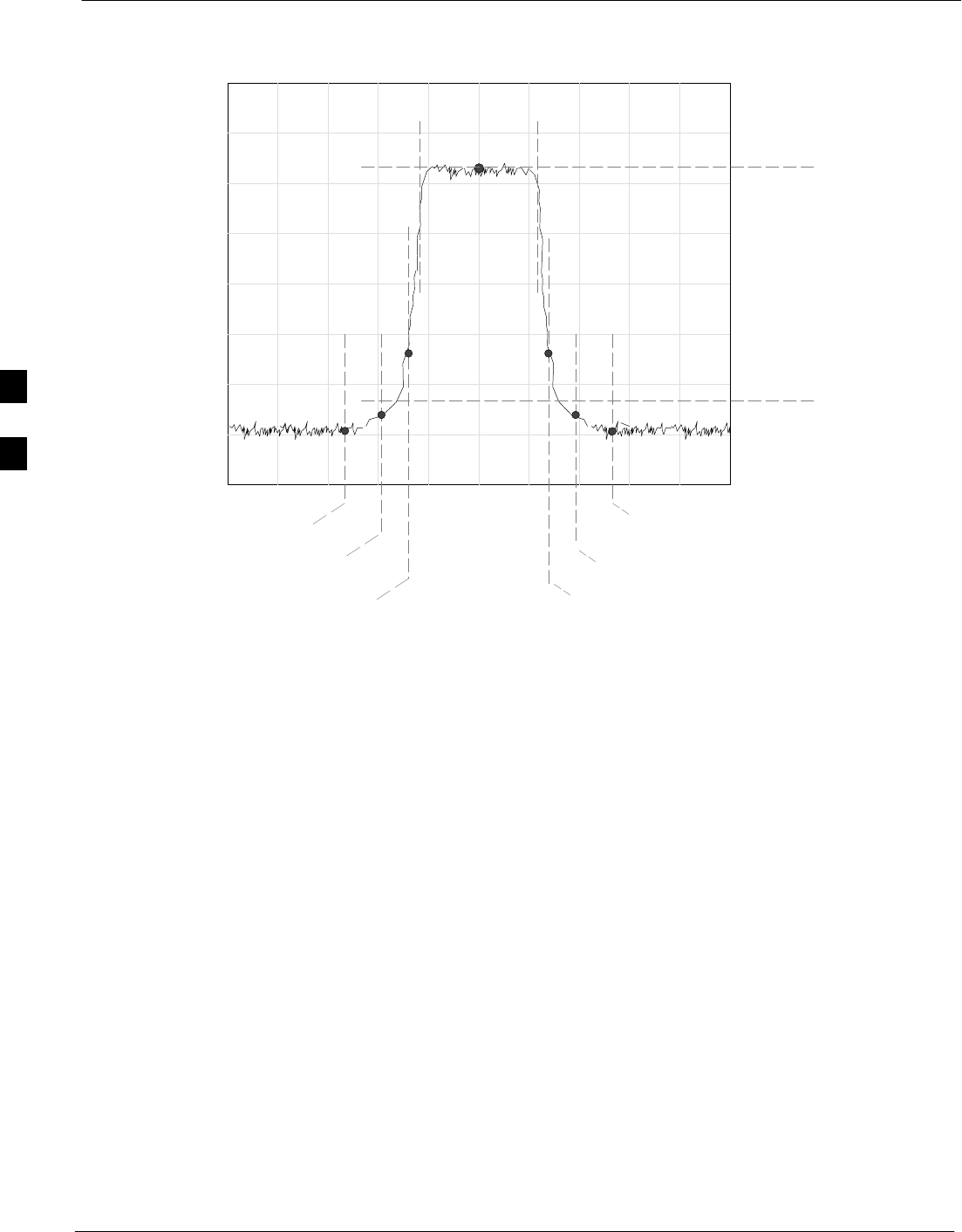
Test Measurements - The test equipment will measure and return the
attenuation level in dB of all spurious and IM products with respect to
the mean power of the CDMA channel measured in a 1.23 MHz
bandwidth, verifying that results meet system tolerances at the following
test points (see also Figure 4-2):
SFor 800 MHz:
- At least -45 dB @ + 750 kHz from center frequency
- At least -45 dB @ - 750 kHz from center frequency
- At least -60 dB @ - 1980 kHz from center frequency
- At least -60 dB @ + 1980 kHz from center frequency
SFor 1.9 GHz:
- At least -45 dB @ + 885 kHz from center frequency
- At least -45 dB @ - 885 kHz from center frequency
- At least -55 dB @ - 1980 kHz from center frequency
- At least -55 dB @ + 1980 kHz from center frequency
Redundant BBX Testing - The BBX will then de-key, and if selected,
the redundant BBX will be assigned to the current TX antenna path
under test. The test will then be repeated.
4

TX Spectral Purity Transmit Mask Acceptance Test68P09255A69-3
Aug 2002 1X SCt4812ET Lite BTS Optimization/ATP Software Release 2.16.1.x
PRELIMINARY
4-17
Spectral Purity TX Mask Acceptance Test
Follow the steps in Table 4-8 to verify the transmit spectral mask
specification on the TX antenna paths for the selected BBXs.
Table 4-8: Test Spectral Purity Transmit Mask
Step Action
1Set up the test equipment for TX acceptance tests per Table 4-3.
2Select the BBXs to be tested.
3If the Test Pattern to be used is Standard, CDFPilot, or CDF; select at least one MCC (Refer to
“Test Pattern Drop-down Pick List” on page 3-83.)
4Click on Tests in the BTS menu bar, and select TX > TX Mask... from the pull-down menus.
5Select the appropriate carrier(s) and sector(s) (carrier-bts#-sector#-carrier#) from those displayed in the
Channels/Carrier pick list.
NOTE
To select multiple items, hold down the Shift or Ctrl key while clicking on pick list items to select
multiple carrier(s)-sector(s).
6Verify that the correct channel number for the selected carrier is shown in the Carrier # Channels
box.
- If it is not, obtain the latest bts-#.cdf and cbsc-#.cdf files from the CBSC.
NOTE
If necessary, the correct channel number may be manually entered into the Carrier # Channels box.
7If at least one MCC was selected in Step 3, select the appropriate transfer rate (1 = 9600, 3 = 9600 1X)
from the drop-down list in the Rate Set box.
NOTE
The Rate Set selection of 3 is only available if 1X cards are selected for the test.
8In the Test Pattern box, select the test pattern to use for the calibration from the drop-down list (refer
to “Test Pattern Drop-down Pick List” under “TX Calibration and the LMF” in the Bay Level Offset
Calibration section of Chapter 3).
9 Click OK to display a status bar followed by a Directions pop-up window.
10 Follow the cable connection directions as they are displayed, and click the Continue button to begin
testing.
- As the ATP process is completed, results will be displayed in a status report window.
11 Click the Save Results or Dismiss button.
NOTE
If Dismiss is used, the test results will not be saved in the test report file.
4
TX Spectral Purity Transmit Mask Acceptance Test 68P09255A69-3
Aug 2002
1X SCt4812ET Lite BTS Optimization/ATP Software Release 2.16.1.x
PRELIMINARY
4-18
Figure 4-2: TX Mask Verification Spectrum Analyzer Display
- 885 kHz + 885 kHz
Center Frequency Reference
Attenuation level of all
spurious and IM products
with respect to the mean
power of the CDMA channel
.5 MHz Span/Div
Ampl 10 dB/Div
Mean CDMA Bandwidth
Power Reference
- 1980 kHz
+750 kHz
+ 1980 kHz
- 750 kHz
4

TX Waveform Quality (Rho) Acceptance Test68P09255A69-3
Aug 2002 1X SCt4812ET Lite BTS Optimization/ATP Software Release 2.16.1.x
PRELIMINARY
4-19
TX Waveform Quality (Rho) Acceptance Test
Background
Overview - This test verifies the transmitted pilot channel element
digital waveform quality of each operator-selected BBX carrier keyed up
at a specific frequency specified in the current CDF. All tests are
performed using the external, calibrated test equipment controlled by the
same command. All measurements are made at the appropriate TX
antenna connector.
Equipment Operation During Testing - Pilot gain will be set to 262
for each antenna, and all TCH elements from the MCCs will be
forward-link disabled. The selected BBXs will be keyed up using both
bbxlvl and BLO to generate a CDMA carrier (with pilot channel
element only, Walsh code 0). RF output power is set at 40 dBm as
measured at the appropriate BTS TX antenna connector.
Test Measurements - The test equipment will measure and return the
pilot channel element digital waveform quality (rho) percentage,
verifying that the result meets the following specification:
Waveform quality (Rho) should be > 0.912.
Redundant BBX Testing - The BBX will then de-key, and if selected,
the redundant BBX will be assigned to the current TX antenna path
under test. The test will then be repeated for the redundant BBX.
Waveform Quality (Rho) Acceptance Test
Follow the steps in Table 4-9 to verify the pilot channel element
waveform quality (rho) on the TX antenna paths for the selected BBXs.
Table 4-9: Test Waveform Quality (Rho)
Step Action
1Set up the test equipment for TX acceptance tests per Table 4-3.
2Select the BBXs to be tested.
3Click on Tests in the BTS menu bar, and select TX > Rho... from the pull-down menus.
4Select the appropriate carrier(s) and sector(s) (carrier-bts#-sector#-carrier#) from those displayed in the
Channels/Carrier pick list.
NOTE
To select multiple items, hold down the Shift or Ctrl key while clicking on pick list items to select
multiple carrier(s)-sector(s).
5Verify that the correct channel number for the selected carrier is shown in the Carrier # Channels
box.
- If it is not, obtain the latest bts-#.cdf and cbsc-#.cdf files from the CBSC.
NOTE
If necessary, the correct channel number may be manually entered into the Carrier # Channels box.
. . . continued on next page
4

TX Waveform Quality (Rho) Acceptance Test 68P09255A69-3
Aug 2002
1X SCt4812ET Lite BTS Optimization/ATP Software Release 2.16.1.x
PRELIMINARY
4-20
Table 4-9: Test Waveform Quality (Rho)
Step Action
6 Click OK to display a status bar followed by a Directions pop-up window.
7Follow the cable connection directions as they are displayed, and click the Continue button to begin
testing.
- As the ATP process is completed, results will be displayed in a status report window.
8Click the Save Results or Dismiss button.
NOTE
If Dismiss is used, the test results will not be saved in the test report file.
4

TX Pilot Time Offset Acceptance Test68P09255A69-3
Aug 2002 1X SCt4812ET Lite BTS Optimization/ATP Software Release 2.16.1.x
PRELIMINARY
4-21
TX Pilot Time Offset Acceptance Test
Background
Overview - This test verifies the transmitted pilot channel element Pilot
Time Offset of each operator-selected BBX carrier keyed up at a specific
frequency specified in the current CDF. All tests will be performed using
the external, calibrated test equipment controlled by the same command.
All measurements will be made at the BTS TX antenna connector.
Equipment Operation During Testing - The pilot gain will be set to
262 for each antenna and all TCH elements from the MCCs will be
forward-link disabled. The selected BBXs will be keyed using both
bbxlvl and BLO to generate a CDMA carrier (with pilot channel
element only, Walsh code 0). TX power output is set at 40 dBm as
measured at the TX output.
Test Measurements - The test equipment will measure and return the
Pilot Time Offset in ms, verifying that results meet the following
specification:
Pilot Time Offset should be within 3 ms of the target PT Offset
(zero ms).
Redundant BBX Testing - The BBX will then de-key, and if selected,
the redundant BBX will be assigned to the current TX antenna path
under test. The test will then be repeated for the redundant BBX.
NOTE This test also executes and returns the TX Frequency and TX
Waveform Quality (rho) ATP tests, however, only Pilot Time
Offset results are written to the ATP test report.
Pilot Time Offset Acceptance Test
Follow the steps in Table 4-10 to verify the Pilot Time Offset on the TX
antenna paths for the selected BBXs.
Table 4-10: Test Pilot Time Offset
Step Action
1Set up the test equipment for TX acceptance tests per Table 4-3.
2Select the BBXs to be tested.
3Click on Tests in the BTS menu bar, and select TX > Pilot Time Offset... from the pull-down menus.
4Select the appropriate carrier(s) and sector(s) (carrier-bts#-sector#-carrier#) from those displayed in the
Channels/Carrier pick list.
NOTE
To select multiple items, hold down the Shift or Ctrl key while clicking on pick list items to select
multiple carrier(s)-sector(s).
. . . continued on next page
4

TX Pilot Time Offset Acceptance Test 68P09255A69-3
Aug 2002
1X SCt4812ET Lite BTS Optimization/ATP Software Release 2.16.1.x
PRELIMINARY
4-22
Table 4-10: Test Pilot Time Offset
Step Action
5Verify that the correct channel number for the selected carrier is shown in the Carrier # Channels
box.
- If it is not, obtain the latest bts-#.cdf and cbsc-#.cdf files from the CBSC.
NOTE
If necessary, the correct channel number may be manually entered into the Carrier # Channels box.
6 Click OK to display a status bar followed by a Directions pop-up window.
7Follow the cable connection directions as they are displayed, and click the Continue button to begin
testing.
- As the ATP process is completed, results will be displayed in a status report window.
8Click the Save Results or Dismiss button.
NOTE
If Dismiss is used, the test results will not be saved in the test report file.
4

TX Code Domain Power/Noise Floor Acceptance Test68P09255A69-3
Aug 2002 1X SCt4812ET Lite BTS Optimization/ATP Software Release 2.16.1.x
PRELIMINARY
4-23
TX Code Domain Power/Noise Floor Acceptance Test
Background
Overview - This test verifies the Code Domain Power and Noise Floor
of each operator-selected BBX carrier keyed at a specific frequency
specified in the current CDF. All tests are performed using the external,
calibrated test equipment controlled by the same command. All
measurements are made at the appropriate BTS TX antenna connector.
CDMA Channel Test Set-up - Pilot gain will be set to 262 for each
antenna and the selected MCCs will be configured to supply all
odd-numbered Walsh code traffic channel elements by enabling
Orthogonal Channel Noise Source (OCNS) on all odd MCC channel
elements (maximum 32 full rate channels with an OCNS gain of 81). All
even-numbered Walsh code traffic channel elements will not have
OCNS enabled, and are considered “OFF”. Selected MCCs will be
forward-link enabled for the antenna (sector) under test.
Equipment Operation During Testing - The BBX will be keyed up
using a BLO-corrected bbxlvl value to generate a CDMA carrier
consisting of pilot and OCNS channels. RF output power, as measured at
the appropriate frame TX antenna connector, is set at one of the
following values depending on the operating frequency spectrum:
S800 MHz: 33.5 dBm
S1.9 GHz: 31.0 dBm
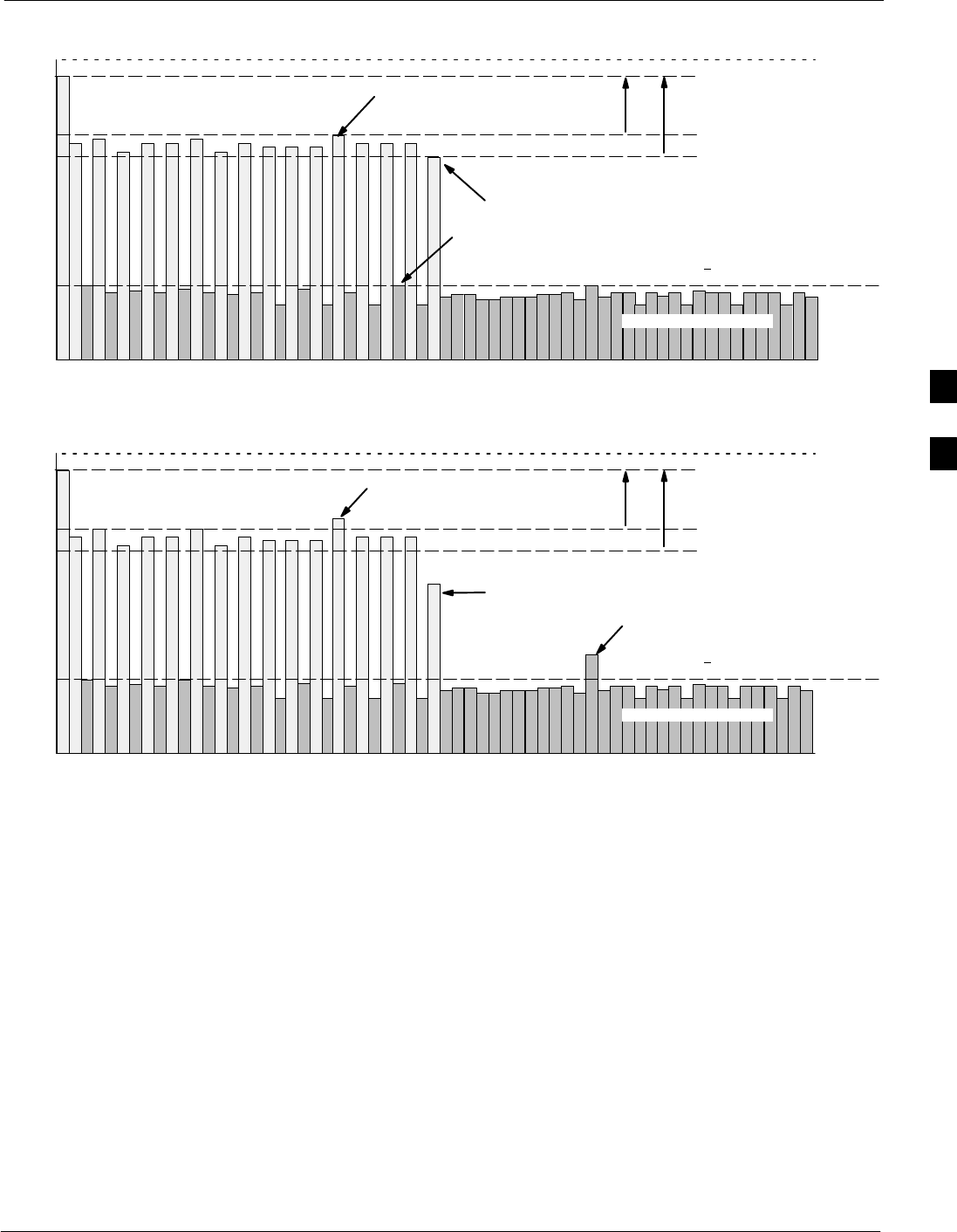
Test Measurements - The test equipment will measure and return the
channel element power in dB of all specified Walsh channels within the
CDMA spectrum. Additional calculations will be performed to verify the
following parameters are met (refer to Figure 4-3 for graphic
representations):
STraffic channel element power level will be verified by calculating the
ratio of Pilot power to OCNS gain of all traffic channels (root sum of
the square (RSS) of each OCNS gain divided by the Pilot power).
This value should be 10.2 dB + 2.0 dB.
SNoise floor (unassigned “OFF” even-numbered Walsh channels) is
verified to be < -27 dB for IS-95A/B and CDMA2000 1X with
respect to total CDMA channel power.
NOTE When performing this test using the LMF and the MCC is an
MCC8E or MCC24E, the redundant BBX may fail or show
marginal performance. This is due to a timing mismatch that the
LMF does not address. Performing this test from the CBSC will
not have this timing problem.
Redundant BBX Testing - The BBX will then de-key, and if selected,
the redundant BBX will be assigned to the current TX antenna path
under test. The test will then be repeated for the redundant BBX. Upon
completion of the test, OCNS channels will be disabled on the specified
MCC channel elements.
4

TX Code Domain Power/Noise Floor Acceptance Test 68P09255A69-3
Aug 2002
1X SCt4812ET Lite BTS Optimization/ATP Software Release 2.16.1.x
PRELIMINARY
4-24
Code Domain Power/Noise Floor Test
Follow the steps in Table 4-11 to verify the Code Domain Power/Noise
floor of each selected BBX carrier keyed up at a specific frequency.
Table 4-11: Test Code Domain Power/Noise Floor
Step Action
1Set up the test equipment for TX acceptance tests per Table 4-3.
2Select the BBXs and MCCs to be tested.
3Click on Tests in the BTS menu bar, and select TX > Code Domain Power... from the pull-down
menus.
4Select the appropriate carrier(s) and sector(s) (carrier-bts#-sector#-carrier#) from those displayed in the
Channels/Carrier pick list.
NOTE
To select multiple items, hold down the Shift or Ctrl key while clicking on pick list items to select
multiple carrier(s)-sector(s).
5Verify that the correct channel number for the selected carrier is shown in the Carrier # Channels
box.
- If it is not, obtain the latest bts-#.cdf and cbsc-#.cdf files from the CBSC.
NOTE
If necessary, the correct channel number may be manually entered into the Carrier # Channels box.
6If at least one MCC was selected in Step 3, select the appropriate transfer rate (1 = 9600, 3 = 9600 1X)
from the drop-down list in the Rate Set box.
NOTE
The Rate Set selection of 3 is only available if 1X cards are selected for the test.
7 Click OK to display a status bar followed by a Directions pop-up window.
8Follow the cable connection directions as they are displayed, and click the Continue button to begin
testing.
- As the ATP process is completed, results will be displayed in a status report window.
9Click the Save Results or Dismiss button.
NOTE
If Dismiss is used, the test results will not be saved in the test report file.
4
TX Code Domain Power/Noise Floor Acceptance Test68P09255A69-3
Aug 2002 1X SCt4812ET Lite BTS Optimization/ATP Software Release 2.16.1.x
PRELIMINARY
4-25
Pilot Channel
Active channels
PILOT LEVEL
MAX OCNS SPEC.
MIN OCNS SPEC.
MAXIMUM NOISE FLOOR:
< -27 dB FOR IS-95A/B AND
CDMA2000 1X
Inactive channels
Walsh 0 1 2 3 4 5 6 7 ... 64
MAX OCNS
CHANNEL
MIN OCNS
CHANNEL
8.2 dB 12.2 dB
MAX NOISE
FLOOR
Pilot Channel
Active channels
PILOT LEVEL
MAX OCNS SPEC.
MIN OCNS SPEC.
MAXIMUM NOISE FLOOR:
< -27 dB FOR IS-95A/B AND
CDMA2000 1X
Inactive channels
Walsh 0 1 2 3 4 5 6 7 ... 64
FAILURE - DOES NOT
MEET MIN OCNS SPEC.
FAILURE - EXCEEDS
MAX OCNS SPEC. 8.2 dB 12.2 dB
FAILURE - EXCEEDS MAX
NOISE FLOOR SPEC.
Code Domain Power/Noise Floor (OCNS Pass) Example
Figure 4-3: Code Domain Analyzer CD Power/Noise Floor Display Examples
Code Domain Power/Noise Floor (OCNS Failure) Example
4

RX FER Acceptance Test 68P09255A69-3
Aug 2002
1X SCt4812ET Lite BTS Optimization/ATP Software Release 2.16.1.x
PRELIMINARY
4-26
RX FER Acceptance Test
Background
Overview - This test verifies the BTS Frame Erasure Rate (FER) on all
TCHs currently configured on operator-selected MCCs (full rate at 1%
FER) at -119 dBm. All tests are performed using the external, calibrated
test equipment as the signal source controlled by the same command.
Measurements are made at the specified BTS RX antenna connection.
Equipment Operation During Testing - The pilot gain on each MCC
will be set to 262 for each TX antenna, and the forward link for all TCH
elements from the MCCs will be enabled. Appropriate BBX(s) must be
keyed in order to enable the RX receive circuitry. Operator-selected
BBXs will be keyed using only bbxlvl, to generate a CDMA carrier
with pilot channel element only. Transmit power output is set at -40
dBm. Test equipment output power is set so that the received power at
the BBX is -119 dBm. The final output power setting of the test
equipment takes into account the MPC type, BTS RF path losses, and
test cable losses. If selected, the redundant BBX will be assigned to the
current RX antenna paths under test.
Test Measurements - The LMF will prompt the MCC channel element
under test to measure all-zero longcode and provide the FER report on
the selected active MCC on the reverse link for the main and, if selected,
diversity RX antenna paths. Results are evaluated to ensure they meet
the following specification:
FER returned less than 1% and Total Frames measured is 1500
Redundant BBX Testing - After the test, the BBX and the test
equipment will be de-keyed to shut down the pilot signal and the active
channel element, respectively. If the redundant BBX was tested, BBXR
assignment to an active sector will also be reset.
Antenna Connections for Companion Frame RX Diversity Tests - At
a site equipped with companion frames, RX diversity for each
SC4812ET Lite frame is provided by the receive antennas for the
collocated companion frame. Because of this, performing FER on
companion frame diversity RX requires different RX test cable
connections than on a starter frame. When performing companion frame
diversity RX FER, use Figure 4-1 and Table 4-1 or Table 4-2 to
determine the correct location for the RX test cable connections.
4

RX FER Acceptance Test68P09255A69-3
Aug 2002 1X SCt4812ET Lite BTS Optimization/ATP Software Release 2.16.1.x
PRELIMINARY
4-27
FER Acceptance Test
Follow the steps in Table 4-12 to verify the FER on RX antenna paths
using selected MCCs and BBXs.
Table 4-12: Test FER
Step Action
1Set up the test equipment for RX acceptance tests per Table 4-3.
2If a companion frame is being tested and either BOTH or DIV is to be selected in step 7, perform the
additional test equipment set-up in Table 4-4 for the diversity RX portion of the ATP.
NOTE
If the LMF has been logged into the BTS with a different Multi-Channel Preselector setting than the
one to be used for this test, the LMF must be logged out of the BTS and logged in again with the new
Multi-Channel Preselector setting. Using the wrong MPC setting can cause a false test failure.
3Select the BBXs and MCCs to be tested.
4Click on Tests in the BTS menu bar, and select RX > FER... from the pull-down menu.
5Select the appropriate carrier(s) and sector(s) (carrier-bts#-sector#-carrier#) from those displayed in the
Channels/Carrier pick list.
NOTE
To select multiple items, hold down the Shift or Ctrl key while clicking on pick list items to select
multiple carrier(s)-sector(s).
6Verify that the correct channel number for the selected carrier is shown in the Carrier # Channels
box.
- If it is not, obtain the latest bts-#.cdf and cbsc-#.cdf files from the CBSC.
NOTE
If necessary, the correct channel number may be manually entered into the Carrier # Channels box.
7NOTE
If a companion frame with the inter-frame diversity RX cabling disconnected is being tested do not
select BOTH in this step. The RX main and diversity paths must be tested separately for this
configuration because each requires a different Multi-Coupler Preselector type to provide the proper
test signal gain.
Select the appropriate RX branch (Both, Main, or Diversity) in the drop-down list.
8In the Rate Set box, select the appropriate data rate (1=9600, 2=14400, 3=9600 1X) from the
drop-down list.
NOTE
The Rate Set selection of 2 is only available if non-1X cards are selected for the test.
The Rate Set selection of 3 is only available if 1X cards are selected for the test.
9 Click OK to display a status bar followed by a Directions pop-up window.
10 NOTE
When testing diversity RX paths on companion frames, be sure to follow the RX test cable connection
information in Table 4-1 or Table 4-2, as applicable, during this step.
Follow cable connection directions as they are displayed, and click the Continue button to begin
testing.
- As the ATP process is completed, results will be displayed in the status report window.
. . . continued on next page
4

RX FER Acceptance Test 68P09255A69-3
Aug 2002
1X SCt4812ET Lite BTS Optimization/ATP Software Release 2.16.1.x
PRELIMINARY
4-28
Table 4-12: Test FER
Step Action
11 Click the Save Results or Dismiss button.
NOTE
If Dismiss is used, the test results will not be saved in the test report file.
4

Generating an ATP Report68P09255A69-3
Aug 2002 1X SCt4812ET Lite BTS Optimization/ATP Software Release 2.16.1.x
PRELIMINARY
4-29
Generating an ATP Report
Background
Each time an ATP test is run, ATP data is updated and must be saved to
an ATP report file using the Save Results button to close the status
report window. The ATP report file will not be updated if the status
reports window is closed using the Dismiss button.
ATP Report
A separate report is created for each BTS and includes the following for
each test:
STest name
SPASS or FAIL
SDescription information (if applicable)
SBBX number
SChannel number
SCarrier number
SSector number
SUpper test limit
SLower test limit
STest result
STime stamp
SDetails/Warning information (if applicable)
Follow the procedures in the Table 4-13 to view and create a printable
file for the ATP report.
Table 4-13: Generating an ATP Report
Step Action
1Click on the Login tab (if not in the forefront).
2Click on the desired BTS in the Available Base Stations pick list to select it.
3Click on the Report button.
4If a printable file is not needed, click on the Dismiss button.
5If a printable file is required, perform the following:
5a - Select the desired file type (text, comma-delimited, HTML) for the report file from the
drop-down list at the bottom of the screen.
5b - Click the Save button to save the file.
-- The file will be saved in the selected format in the bts-# folder for the BTS selected.
4

Aug 2002 1X SCt4812ET Lite BTS Optimization/ATP Software Release 2.16.1.x
PRELIMINARY
5-1
Chapter 5
Leaving the Site
5

Updating Calibration Data Files 68P09255A69-3
Aug 2002
1X SCt4812ET Lite BTS Optimization/ATP Software Release 2.16.1.x
PRELIMINARY
5-2
Updating Calibration Data Files
After completing the TX calibration and audit, updated CAL file
information must be moved from the LMF Windows environment back
to the CBSC, a Unix environment. The following procedures detail
moving files from one environment to the other.
Copying CAL files from LMF to a Diskette
Follow the procedures in Table 5-1 to copy the CAL files from an LMF
computer to a 3.5 diskette.
Table 5-1: Copying CAL Files to a Diskette
Step Action
1 With Windows running on the LMF computer, insert a disk into Drive A:\.
2Launch the Windows Explorer application program from the Start > Programs menu list.
3Select the applicable <x>:\<lmf home directory/cdma/bts-# folder.
4Drag the bts-#.cal file to Drive A.
5Repeat Steps 3 and 4, as required, for other bts-# folders.
Copying CAL Files from Diskette to the CBSC
Follow the procedures in Table 5-2 to copy CAL files from a diskette to
the CBSC.
Table 5-2: Copying CAL Files from Diskette to the CBSC
Step Action
1Log into the CBSC on the OMC-R Unix workstation using your account name and password.
2Place the diskette containing calibration file(s) in the workstation diskette drive.
3Type in eject -q and press the Enter key.
4Type in mount and press the Enter key.
NOTE
SCheck to see that the message “floppy/no_name” is displayed on the last line.
SIf the eject command was previously entered, floppy/no_name will be appended with a number.
Use the explicit floppy/no_name reference displayed.
5Type in cd /floppy/no_name and press the Enter key.
6Type in ls -lia and press the Enter key.
- Verify the bts-#.cal file filename appears in the displayed directory listing.
7Type in cd and press the Enter key.
8Type in pwd and press the Enter key.
- Verify the displayed response shows the correct home directory (/home/<user’s name>).
9 With Solaris versions of Unix, create a Unix-formatted version of the bts-#.cal file in the home
directory by performing the following:
. . . continued on next page
5

Updating Calibration Data Files68P09255A69-3
Aug 2002 1X SCt4812ET Lite BTS Optimization/ATP Software Release 2.16.1.x
PRELIMINARY
5-3
Table 5-2: Copying CAL Files from Diskette to the CBSC
Step Action
9a - Type the following command:
dos2unix /floppy/no_name/bts-#.cal bts-#.cal
Where: # = BTS number for which the CAL file was created
9b - Press the Enter key.
NOTE
Other versions of Unix do not support the dos2unix command. In these cases, use the Unix cp
(copy) command. The copied files will contain DOS line feed characters which must be edited out
with a Unix text editor.
10 Type in ls -l *.cal and press the Enter key. Verify the CAL files have been copied.
- Verify all CAL files to be transferred appear in the displayed listing.
11 Type eject, and press the Enter key.
12 Remove the diskette from the workstation.
5

Prepare to Leave the Site 68P09255A69-3
Aug 2002
1X SCt4812ET Lite BTS Optimization/ATP Software Release 2.16.1.x
PRELIMINARY
5-4
Prepare to Leave the Site
Removing External Test Equipment
Perform the procedure in Table 5-3 to disconnect the test equipment and
configure the BTS for active service.
Table 5-3: Remove External Test Equipment
Step Action
1n WARNING
Be sure no BBXs are keyed before performing this step. Failure to do so can result in personal injury
and damage to BTS LPAs.
Disconnect all external test equipment from all TX and RX connectors at the rear of the frame.
2Reconnect and visually inspect all TX and RX antenna feed lines at the frame RF interface panel.
NOTE
Verify that all sector antenna feed lines are connected to the correct antenna connectors on the frame.
Crossed antenna cables will degrade call processing.
Reset All Devices and Initialize Site Remotely
Generally, devices in the BTS should not be left with data and code
loaded from the LMF. The configuration data and code loads used for
normal operation could be different from those stored in the LMF files.
By resetting all devices, the required data and code can be loaded from
the CBSC using the DLM when spans are again active.
To reset all devices and have the OMCR/CBSC bring up the site
remotely, perform the procedure in Table 5-4.
Table 5-4: Reset BTS Devices and Remote Site Initialization
Step Action
1Terminate the LMF session by following the procedures in Table 5-6.
2Cycle BTS power off, as specified in Table 2-9 and Table 2-10, and on, as specified in Table 2-11 and
Table 2-12.
3Reconnect spans by following the procedure in Table 5-7.
4Notify the OMCR/CBSC to take control of the site and download code and data to the BTS.
5Verify the CBSC can communicate with the GLIs.
5

Prepare to Leave the Site68P09255A69-3
Aug 2002 1X SCt4812ET Lite BTS Optimization/ATP Software Release 2.16.1.x
PRELIMINARY
5-5
Bringing Modules into Service with the LMF
NOTE Whenever possible, have the CBSC/MM bring up the site and
enable all devices at the BTS.
If there is a reason code and/or data should or could not be loaded
remotely from the CBSC, follow the steps outlined in Table 5-5 as
required to bring BTS processor modules from OOS to INS state.
Table 5-5: Bring Modules into Service
Step Action
1In the LMF GUI environment, select the device(s) to be enabled by clicking on each one.
NOTE
SThe MGLI and CSM must be INS_ACT (bright green) before an MCC can be enabled.
SProcessors which must be enabled and the order of enabling are as follows:
1. MGLI
2. CSMs
3. MCCs
2Click on Device in the BTS menu bar, and select Enable from the pull-down list.
- A status report window is displayed.
NOTE
If a BBX is selected, a transceiver parameters window is displayed to collect keying information. Do
not enable the BBX.
3 Click Cancel to close the transceiver parameters window, if applicable.
4 Click OK to close the status report window.
- The color of devices which successfully change to INS will change bright green.
Terminating LMF Session/Removing Terminal
Perform the procedure in Table 5-6 as required to terminate the LMF
GUI session and remove the LMF computer.
Table 5-6: Remove LMF
Step Action
1! CAUTION
Do not power down the LMF terminal without performing the procedure below. Corrupted/lost
data files may result.
Log out of all BTS sessions and exit LMF by clicking on File in the LMF window menu bar and select-
ing Logout and Exit from the pull-down list.
2In the Windows Task Bar, click Start and select Shutdown.
3 Click Yes when the Shut Down Windows message appears
4Wait for the system to shut down and the screen to go blank.
. . . continued on next page
5

Prepare to Leave the Site 68P09255A69-3
Aug 2002
1X SCt4812ET Lite BTS Optimization/ATP Software Release 2.16.1.x
PRELIMINARY
5-6
Table 5-6: Remove LMF
Step Action
5Disconnect the LMF terminal Ethernet port from the BTS frame.
6Disconnect the LMF terminal serial port, the RS-232-to-GPIB interface box, and the GPIB
cables as required for equipment transport.
Connecting BTS T1/E1 Spans
Before leaving the site, connect any T1 or E1 span connectors removed
previously to allow the LMF to control the BTS. Refer to Table 5-7 and
Figure 3-2.
Table 5-7: Connect T1 or E1 Spans
Step Action
1Re-connect any disconnected span connectors to the Span I/O A and B boards.
2If equipped, ensure the CSU is powered on.
3Verify span status, ensuring the OMC-R/CBSC can communicate with the BTS.
Before Leaving the site
Be sure all requirements listed in Table 5-8 are completed before leaving
the site.
Table 5-8: Check Before Leaving the Site
Step Action
1When backup batteries are installed, all battery circuit breakers are ON (pushed in).
2Both heat exchanger circuit breakers on the DC PDA are set to ON (pushed in), and the heat
exchanger blowers are running.
3The External Blower Assembly (EBA) power cable is connected, and the EBA is running.
4The MAP power switch is set to ON, and the POWER (green) LED is lighted.
5The MAP TCP switch is set to ON.
6The BATT TEST switch on the MAP is set to OFF, and the BATT. TEST (amber) LED is not lighted.
7No alarm conditions are being reported to the CBSC with all frame doors closed.
5

Aug 2002 1X SCt4812ET Lite BTS Optimization/ATP Software Release 2.16.1.x
PRELIMINARY
6-1
Chapter 6
Basic Troubleshooting
6

Basic Troubleshooting: Overview 68P09255A69-3
Aug 2002
1X SCt4812ET Lite BTS Optimization/ATP Software Release 2.16.1.x
PRELIMINARY
6-2
Basic Troubleshooting: Overview
Overview
The information in this chapter addresses some of the scenarios likely to
be encountered by Customer Field Engineering (CFE) team members
while performing BTS optimization and acceptance testing. This
troubleshooting guide was created as an interim reference document for
use in the field. It provides “what to do if” basic troubleshooting
suggestions when the BTS equipment does not perform according to the
procedures documented in the manual.
Comments are consolidated from inputs provided by CFEs and
information gained from experience in Motorola labs and classrooms.
6

Troubleshooting: Installation68P09255A69-3
Aug 2002 1X SCt4812ET Lite BTS Optimization/ATP Software Release 2.16.1.x
PRELIMINARY
6-3
Troubleshooting: Installation
Cannot Log into Cell-Site
Table 6-1: Login Failure Troubleshooting Procedures
nStep Action
1If the MGLI LED is solid RED, it implies a hardware failure. Reset MGLI by re-seating it. If this
persists, install GLI card in MGLI slot and retry. A Red LED may also indicate no termination on
an external LAN connector (power entry compartment at rear of frame).
2Verify that the span line is disconnected at the Span I/O card. If the span is still connected, verify
the CBSC has disabled the BTS.
3Try to ‘ping’ the MGLI.
4Verify the LMF is connected to the primary LAN (LAN A) at the LAN shelf below the SCCP
cage. If LAN A is not the active LAN, force a LAN switch to LAN A by following the procedure
in Table 6-2.
5Verify the LMF was configured properly.
6If a Xircom parallel BNC LAN interface is being used, verify the BTS-LMF cable is RG-58
(flexible black cable less than 2.5 feet in length).
7Verify the external LAN connectors are properly terminated (power entry compartment at rear of
frame).
8Verify a T-adapter is not used on LMF computer side connector when connected to the primary
LAN at the LAN shelf.
9Try connecting to the Ethernet Out port in the power entry compartment (rear of frame). Use a
TRB-to-BNC (triax-to-coax) adapter at the LAN connector for this connection.
10 Re-boot the LMF and retry.
11 Re-seat the MGLI and retry.
12 Verify GLI IP addresses are configured properly by following the procedure in Table 6-3.
Table 6-2: Force Ethernet LAN A to Active State as Primary LAN
nStep Action
1If LAN A is not the active LAN, make certain all external LAN connectors are either terminated
with 50Ω loads or cabled to another frame.
2If it has not already been done, connect the LMF computer to the stand-alone or starter frame, as
applicable (Table 3-10).
3If it has not already been done, start a GUI LMF session and log into the BTS on the active LAN
(Table 3-11).
4Remove the 50Ω termination from the LAN B IN connector in the power entry compartment at the
rear of the stand-alone or starter frame. The LMF session will become inactive.
5Disconnect the LMF computer from the LAN shelf LAN B connector and connect it to the LAN A
connector.
. . . continued on next page
6

Troubleshooting: Installation 68P09255A69-3
Aug 2002
1X SCt4812ET Lite BTS Optimization/ATP Software Release 2.16.1.x
PRELIMINARY
6-4
Table 6-2: Force Ethernet LAN A to Active State as Primary LAN
nActionStep
6If the LAN was successfully forced to an active state (the cards in any cage can be selected and
statused), proceed to step 13.
7With the 50Ω termination still removed from the LAN B IN connector, remove the 50Ω
termination from LAN B OUT connector. If more than one frame is connected to the LAN,
remove the termination from the last frame in the chain.
8If the LAN was successfully forced to an active state (the cards in any cage can be selected and
statused), proceed to step 13.
9With the 50Ω terminations still removed from LAN B, unseat each GLI card in each frame
connected to the LAN, until all are disconnected from the shelf backplanes.
10 Reseat each GLI card until all are reconnected.
11 Allow the GLIs to power up, and attempt to select and status cards in the CCP shelves. If LAN A
is active, proceed to step 13.
12 If LAN A is still not active, troubleshoot or continue troubleshooting following the procedures in
Table 6-1.
13 Replace the 50Ω terminations removed from the LAN B IN and OUT connectors.
Table 6-3: GLI IP Address Setting
nStep Action
1If it has not previously been done, establish an MMI communication session with the GLI card as
described in Table 3-15.
2Enter the following command to display the IP address and subnet mask settings for the card:
config lg0 current
A response similar to the following will be displayed:
GLI2>config lg0 current
lg0: IP address is set to
DEFAULT (configured based on card location)
lg0: netmask is set to
DEFAULT (255.255.255.128)
. . . continued on next page
6

Troubleshooting: Installation68P09255A69-3
Aug 2002 1X SCt4812ET Lite BTS Optimization/ATP Software Release 2.16.1.x
PRELIMINARY
6-5
Table 6-3: GLI IP Address Setting
nActionStep
3If the IP address setting response shows an IP address rather than “Default (configured
based on card location),” enter the following:
config lg0 ip default
A response similar to the following will be displayed:
GLI2>config lg0 ip default
_param_config_lg0_ip(): param_delete(): 0x00050001
lg0: ip address set to DEFAULT
4If the GLI subnet mask setting does not display as “DEFAULT (255.255.255.128),” set it to
default by entering the following command:
config lg0 netmask default
A response similar to the following will be displayed:
GLI2>config lg0 netmask default
_param_config_lg0_netmask(): param_delete(): 0x00050001
lg0: netmask set to DEFAULT
5Set the GLI route default to default by entering the following command:
config route default default
A response similar to the following will be displayed:
GLI2>config route default default
_esh_config_route_default(): param_delete(): 0x00050001
route: default gateway set to DEFAULT
6NOTE
Changes to the settings will not take effect unless the GLI is reset.
When changes are completed, close the MMI session, and reset the GLI card.
. . . continued on next page
6

Troubleshooting: Installation 68P09255A69-3
Aug 2002
1X SCt4812ET Lite BTS Optimization/ATP Software Release 2.16.1.x
PRELIMINARY
6-6
Table 6-3: GLI IP Address Setting
nActionStep
7Once the GLI is reset, re-establish MMI communication with it and issue the following command
to confirm its IP address and subnet mask settings:
config lg0 current
A response similar to the following will be displayed:
GLI2>config lg0 current
lg0: IP address is set to
DEFAULT (configured based on card location)
lg0: netmask is set to
DEFAULT (255.255.255.128)
8Repeat steps 1 through 7 for all remaining GLIs, including those in any additional,
inter-connected frames.
Cannot Communicate with Power Meter
Table 6-4: Troubleshooting a Power Meter Communication Failure
nStep Action
1Verify power meter is connected to LMF with GPIB adapter.
2Verify cable connections as specified in Chapter 3.
3Verify the GPIB address of the power meter is set to the same value displayed in the applicable
GPIB address box of the LMF Options window Test Equipment tab. Refer to Table 3-28 or
Table 3-29 and the Setting GPIB Addresses section of Appendix NO TAG for details.
4Verify the GPIB adapter DIP switch settings are correct. Refer to Test Equipment Preparation
section of Appendix NO TAG for details.
5Verify the GPIB adapter is not locked up. Under normal conditions, only 2 green LEDs must be
‘ON’ (Power and Ready). If any other LED is continuously ‘ON’, then cycle GPIB box power and
retry.
6Verify the LMF computer COM1 port is not used by another application; for example, if a
HyperTerminal window is open for MMI, close it.
7 Reset all test equipment by clicking Util in the BTS menu bar and selecting Test Equipment >
Reset from the pull-down lists.
6

Troubleshooting: Installation68P09255A69-3
Aug 2002 1X SCt4812ET Lite BTS Optimization/ATP Software Release 2.16.1.x
PRELIMINARY
6-7
Cannot Communicate with Communications System Analyzer
Table 6-5: Troubleshooting a Communications System Analyzer Communication Failure
nStep Action
1Verify analyzer is connected to LMF with GPIB adapter.
2Verify cable connections as specified in Chapter 3.
3Verify the analyzer GPIB address is set to the same value displayed in the applicable GPIB
address box of the LMF Options window Test Equipment tab. Refer to Table 3-28 or Table 3-29
and the Setting GPIB Addresses section of Appendix F for details.
4Verify the GPIB adapter DIP switch settings are correct. Refer to Test Equipment Preparation
section of Appendix NO TAG for details.
5Verify the GPIB adapter is not locked up. Under normal conditions, only 2 green LEDs must be
‘ON’ (Power and Ready). If any other LED is continuously ‘ON’, then cycle GPIB box power and
retry.
6Verify the LMF computer COM1 port is not used by another application; for example, if a
HyperTerminal window is open for MMI, close it.
7 Reset all test equipment by clicking Util in the BTS menu bar and selecting Test Equipment >
Reset from the pull-down lists.
Cannot Communicate with Signal Generator
Table 6-6: Troubleshooting a Signal Generator Communication Failure
nStep Action
1Verify signal generator is connected to LMF with GPIB adapter.
2Verify cable connections as specified in Chapter 3.
3Verify the signal generator GPIB address is set to the same value displayed in the applicable GPIB
address box of the LMF Options window Test Equipment tab. Refer to Table 3-28 or Table 3-29
and the Setting GPIB Addresses section of Appendix NO TAG for details.
4Verify the GPIB adapter DIP switch settings are correct. Refer to Test Equipment Preparation
section of Appendix NO TAG for details.
5Verify the GPIB adapter is not locked up. Under normal conditions, only 2 green LEDs must be
‘ON’ (Power and Ready). If any other LED is continuously ‘ON’, then cycle GPIB box power and
retry.
6Verify the LMF computer COM1 port is not used by another application; for example, if a
HyperTerminal window is open for MMI, close it.
7 Reset all test equipment by clicking Util in the BTS menu bar and selecting Test Equipment >
Reset from the pull-down lists.
6

Troubleshooting: Download 68P09255A69-3
Aug 2002
1X SCt4812ET Lite BTS Optimization/ATP Software Release 2.16.1.x
PRELIMINARY
6-8
Troubleshooting: Download
Table 6-7: Troubleshooting Code Download Failure
nStep Action
1Verify T1 or E1 span is disconnected from the BTS at Site I/O boards (Figure 3-2).
2Verify LMF can communicate with the BTS devices using the LMF Status function.
3Communication with MGLI must first be established before trying to communicate with any other
BTS device. MGLI must be INS_ACT state (bright green).
4Verify the target card is physically present in the cage and powered-up.
5If the target card LED is solid RED, it implies hardware failure. Reset card by re-seating it. If LED
alarm persists, replace with same type of card from another slot and retry.
6Re-seat card and try again.
7If a BBX reports a failure message and is OOS_RAM, the code load was OK. Use the LMF
Status function to verify the load.
8If a BBX or an MCC remains OOS_ROM (blue) after code download, use the LMF
Device > Status function to verify that the code load was accepted.
9If the code load was accepted, use LMF Device > Download > Flash to load RAM code into flash
memory.
Cannot Download DATA to Any Device (Card)
Table 6-8: Troubleshooting Data Download Failure
nStep Action
1Re-seat card and repeat code and data load procedure.
2Verify the ROM and RAM code loads are of the same release by statusing the card. Refer to
Download the BTS section of Chapter G for more information.
6

Troubleshooting: Download68P09255A69-3
Aug 2002 1X SCt4812ET Lite BTS Optimization/ATP Software Release 2.16.1.x
PRELIMINARY
6-9
Cannot ENABLE Device
Before a device can be enabled (placed in service), it must be in the
OOS_RAM state (yellow in LMF display) with data downloaded to the
device. The color of the device on the LMF changes to green once it is
enabled.
The four device states that can be displayed by the LMF are:
SEnabled (bright green, INS_ACT)
SStand-by (olive green, INS_SBY - redundant CSM and GLI only)
SDisabled (yellow, OOS_RAM)
SReset (blue, OOS_ROM)
Table 6-9: Troubleshooting Device Enable (INS) Failure
nStep Action
1Re-seat card and repeat code and data load procedure.
2If CSM cannot be enabled, verify the CDF has correct latitude and longitude data for cell site
location and GPS sync.
3Ensure primary CSM is in INS_ACT (bright green) state.
NOTE
MCCs will not enable without the CSM being INS.
4Verify 19.6608 MHz CSM clock is present; MCCs will not enable without it.
5BBXs should not be enabled for ATP tests.
6If MCCs give “invalid or no system time,” verify the CSM is enabled.
7Log out of the BTS, exit the LMF, restart the application, log into the BTS, and re-attempt
device-enable actions.
LPA Errors
Table 6-10: LPA Errors
nStep Action
1If LPAs give continuous alarms, cycle power with the applicable DC PDA circuit breakers.
2Establish an MMI session with the LPA (Table 3-15), connecting the cable to the applicable MMI
port on the ETIB.
2a - Type alarms at the HyperTerminal window prompt and press Enter.
-- The resulting display may provide an indication of the problem.
2b - Call Field Support for further assistance.
6

Troubleshooting: Calibration 68P09255A69-3
Aug 2002
1X SCt4812ET Lite BTS Optimization/ATP Software Release 2.16.1.x
PRELIMINARY
6-10
Troubleshooting: Calibration
Bay Level Offset Calibration Failure
Table 6-11: Troubleshooting BLO Calibration Failure
nStep Action
1Verify the power meter or communications system analyzer is configured correctly (see the Test
Equipment Set-up section of Chapter 3), and is connected to the proper BTS TX antenna
connector.
2If a power meter is being used:
2a - Re-calibrate the Power Meter and verify it is calibrated correctly with cal factors from the
power sensor (refer to Appendix F).
2b - Verify the power sensor is functioning properly by checking it with the 1-mW (0 dBm) Power
Ref signal.
2c - Verify communication between the LMF and Power Meter is working by checking that the
meter display is showing RES :
3Verify the parameters in the bts-#.cdf file are set correctly for the BTS operating band as
follows:
For 1900 MHz:
Bandclass=1; Freq_Band=16
For 800 MHz:
Bandclass=0; Freq_Band=8
4Verify that no LPA on the carrier is in alarm state (rapidly flashing red LED).
4a - If any are, reset the LPA(s) by pulling the applicable circuit breaker on the DC PDA, and,
after 5 seconds, pushing back in.
5Verify GPIB adapter is not locked up. Under normal conditions, only 2 green LEDs must be ‘ON’
(Power and Ready). If any other LED is continuously ‘ON’, power-cycle (turn power off and on)
the GPIB Box and retry.
6

Troubleshooting: Calibration68P09255A69-3
Aug 2002 1X SCt4812ET Lite BTS Optimization/ATP Software Release 2.16.1.x
PRELIMINARY
6-11
Calibration Audit Failure
Table 6-12: Troubleshooting Calibration Audit Failure
nStep Action
1Verify the power meter or communications system analyzer is configured correctly (see the Test
Equipment Set-up section of Chapter 3), and is connected to the proper BTS TX antenna
connector.
2If a power meter is being used:
2a - Re-calibrate the Power Meter and verify it is calibrated correctly with cal factors from the
power sensor (refer to Appendix F).
2b - Verify the power sensor is functioning properly by checking it with the 1-mW (0 dBm) Power
Ref signal.
2c - Verify communication between the LMF and Power Meter is working by checking that the
meter display is showing RES :
3Verify that no LPA on the carrier is in alarm state (rapidly flashing red LED).
3a - If any are, reset the LPA(s) by pulling the applicable circuit breaker on the DC PDA, and,
after 5 seconds, pushing back in.
4After calibration, the BLO data must be re-loaded to the BBXs before auditing. Click on the
BBX(s), and in the BTS menu bar select Device > Download >BLO.
Re-try the audit.
5Verify GPIB adapter is not locked up. Under normal conditions, only 2 green LEDs must be ‘ON’
(Power and Ready). If any other LED is continuously ‘ON’, power-cycle (turn power off and on)
the GPIB Box and retry.
6If calibration was being performed for the redundant BBX, be sure the Single-Sided BLO
checkbox was not checked in the CDMA Test Parameters test set-up window.
7If additional items, such as directional couplers or combiners, have been installed in the TX path,
be sure that one of the following has been done:
SVerify BLO checkbox in the CDMA Test Parameters test set-up window is unchecked.
SThe additional path losses have been added into each applicable sector using the Util > Edit >
TX Coupler Loss... function.
6

Basic Troubleshooting: RF Path Fault Isolation 68P09255A69-3
Aug 2002
1X SCt4812ET Lite BTS Optimization/ATP Software Release 2.16.1.x
PRELIMINARY
6-12
Basic Troubleshooting: RF Path Fault Isolation
Overview
The optimization (RF path characterization or calibration) and
post-calibration (audit) procedures measure and limit-check the BTS
reported transmit and receive levels of the path from each BBX to the
back of the frame. When a fault is detected, it is specific to a receive or
transmit path. The troubleshooting process in this section determines the
most probable cause of the fault.
As the calibration and audit tests are performed, results are displayed in
the LMF test status report window. When faults are encountered, the test
procedure in progress continues running and displaying any further
faults. If it appears that there are major faults, the test can be aborted.
The test results can be saved to a bts-#.rpt file in the<x>:\<lmf home
directory \cdma\bts-# folder. To do this, close the test status report
window using the Save Results button.
NOTE Closing the test status report window with the Dismiss button
will delete the test results without saving them.
If a test is re-run or a new calibration, audit, or test is run and the results
are saved, the previous test results in the bts-#.rpt file are
overwritten. To prevent losing previous test results in the bts-#.rpt
file, refer to the procedure in Table 4-13 before performing further
testing with the LMF.
If there are major faults, recheck the test equipment attachments for
errors. If none are found, close the test status report window using the
Save Results button, and save the contents of the resulting bts-#.rpt
file as described in Table 4-13. Also, note other specifics about the
failure, and proceed with the fault isolation procedure.
If Every Test Fails
Check the calibration equipment for proper operation by manually
setting the signal generator output attenuator to the lowest output power
setting. Connect the output port to the spectrum analyzer RF input port.
Set the signal generator output attenuator to -90 dBm, and switch on the
RF output. Verify that the spectrum analyzer can receive the signal,
indicate the correct signal strength (accounting for the cable insertion
loss), and indicate the approximate frequency.
Verify BLO Checkbox
When performing a calibration with the TX Calibration... or All
Cal/Audit... functions, the Verify BLO checkbox should normally be
checked. When a calibration fails, determine if any items such as
directional couplers or combiners have been added to the TX path. If
additional items have been installed in the path, try re-running the
calibration with Verify BLO unchecked. If calibration still does not
pass, refer to the following paragraphs and use the TX output fault
isolation flowchart to identify the most probable cause of the failure.
6

Basic Troubleshooting: RF Path Fault Isolation68P09255A69-3
Aug 2002 1X SCt4812ET Lite BTS Optimization/ATP Software Release 2.16.1.x
PRELIMINARY
6-13
Single-Sided BLO Checkbox
When performing a calibration with the TX Calibration... or All
Cal/Audit... functions, the Single-Sided BLO checkbox should not be
checked when the redundant BBX is being calibrated. When a
calibration fails with the redundant BBX selected, try re-running the
calibration with the Single-Sided BLO checkbox unchecked. If the
calibration still fails, refer to the following paragraphs and use the TX
output fault isolation flowchart to identify the most probable cause of the
failure.
If Faults Are Isolated
If the fault reports are isolated between successful path checks, the root
cause of the faults most likely lies with one or more of the Field
Replaceable Unit (FRU) modules. If more than one failure was reported,
look for a common denominator in the data. For example, if any TX test
fails on one sector only, the BBX assigned to that sector (Table 1-5) is a
likely cause. Also, look at the severity of the failure. If the path loss is
just marginally out of the relaxed specification limit during the
post-calibration TX audit, suspect excessive cable loss. If limits are
missed by a wide margin, suspect mis-wired cables or total device
failure. Use the TX output fault isolation flowchart in Figure 6-1 to
identify the strongest possible cause for a failed TX test.
Fault Isolation Flowchart
The flowchart covers the transmit path. Transmit paths usually fail the
lower test limit, indicating excessive loss in some component in the BTS
site or mis-wiring. A failure of an upper limit usually indicates a
problem with the test setup or external equipment. Before replacing a
suspected FRU, always repeat and verify the test results to rule out a
transient condition. If a BBX fails an upper limit in the post-calibration
audit procedure, re-calibrate and verify the out-of-tolerance condition
for that BBX and/or sector before replacement.
Flowchart Prerequisites
Before entering the fault isolation sequence outlined in the flowchart, be
sure the following have been completed:
SGLIs, MCCs, and BBXs have been downloaded with the correct ROM
code, RAM code, and data (Table 3-17, Table 3-18, and Table 3-19).
SMGLI, CSMs, and MCCs are enabled (Table 3-18, Table 3-21, and
Table 3-22, respectively)
SBe sure the LED on the correct CCD card is solid green.
SBe sure no alarms are being reported by opening an LMF alarm
window as outlined in Table 3-53.
6

Basic Troubleshooting: RF Path Fault Isolation 68P09255A69-3
Aug 2002
1X SCt4812ET Lite BTS Optimization/ATP Software Release 2.16.1.x
PRELIMINARY
6-14
TX Power Output Fault Isolation Flowchart
Figure 6-1: TX Output Fault Isolation Flowchart
Start
TX Power
Out of Limits
No
No, everything fails
If equipped, does a
BBX on a different
carrier but for the
same sector
pass?
Yes, it passes.
Likely Cause: Crossed TX cabling to include:
- CIO-trunking module,
- Trunking module-filter/combiner,
- Filter/combiner-DRDC/TRDC
Carrier LPAs
Also check: Carrier trunking module
CIO card.
Did TX Output
fail the High or
Low limit?
High limit
failure. Does
redundant BBX
have the same
problem on the
same sector?
Likely Cause: BBX card
Attempt re-calibration
before replacement.
No
Does any other
sector have the
same problem?
Likely Cause: CIO card
Carrier trunking module
Also check: CIO-trunking module cabling
TX filter/combiner cabling
TX DRDC/TRDC cabling
Likely Cause: External Power Measurement
Equipment and/or Set-up.
Also check: Switch card
External Attenuators & Pads,
Check Site Documentation.
Yes
Yes
Low limit
failure.
Likely Cause: CIO card not fully seated
External Power Measurement
Equipment and/or Set-up
Crossed TX cabling to include:
- CIO-trunking module,
- Trunking module-filter/combiner,
- Filter/combiner-DRDC/TRDC
Yes, it passes.
If equipped, does a
BBX on the same
carrier but for a
different sector
pass?
No, next BBX on same carrier
fails on different sector.
Likely Cause: BBX card
Loose connections on
CIO-trunking module cabling,
TX filter/combiner cabling, or
TX DRDC/TRDC cabling
Also check: CIO card
Carrier trunking module
6

Troubleshooting: Transmit ATP68P09255A69-3
Aug 2002 1X SCt4812ET Lite BTS Optimization/ATP Software Release 2.16.1.x
PRELIMINARY
6-15
Troubleshooting: Transmit ATP
BTS Passed Reduced ATP Tests but Has Forward Link Problem in Normal
Operation
Follow the procedure in Table 6-13 to troubleshoot a forward link
problem during normal operation after passing a reduced ATP.
Table 6-13: Troubleshooting Forward Link Failure (BTS Passed Reduced ATP)
nStep Action
1Perform the following additional tests to troubleshoot a forward link problem:
1a - TX mask
1b - TX rho
1c - TX code domain
Cannot Perform TX Mask Measurement
Table 6-14: Troubleshooting TX Mask Measurement Failure
nStep Action
1Verify that TX audit passes for the BBX(s).
2If performing manual measurement, verify analyzer setup.
3Verify that no LPA in the sector is in alarm state (flashing red LED). Re-set the LPA by pulling the
circuit breaker, and, after 5 seconds, pushing it back in.
Cannot Perform Rho or Pilot Time Offset Measurement
Table 6-15: Troubleshooting Rho and Pilot Time Offset Measurement Failure
nStep Action
1Verify presence of RF signal by switching to spectrum analyzer screen.
2Verify PN offsets displayed on the analyzer is the same as the PN offset in the CDF file.
3Re-load MGLI code and data and repeat the test.
4If performing manual measurement, verify analyzer setup.
5Verify that no LPA in the sector is in alarm state (flashing red LED). Reset the LPA by pulling the
circuit breaker, and, after 5 seconds, pushing back in.
6If Rho value is unstable and varies considerably (e.g. .95,.92,.93), this may indicate that the GPS
is still phasing (trying to reach and maintain 0 freq. error). Go to the freq. bar in the upper right
corner of the Rho meter and select Hz. Press <Shift-avg> and enter 10, to obtain an average Rho
value. This is an indication the GPS has not stabilized before going INS and may need to be
re-initialized.
6

Troubleshooting: Transmit ATP 68P09255A69-3
Aug 2002
1X SCt4812ET Lite BTS Optimization/ATP Software Release 2.16.1.x
PRELIMINARY
6-16
Cannot Perform Code Domain Power and Noise Floor Measurement
Table 6-16: Troubleshooting Code Domain Power and Noise Floor Measurement Failure
nStep Action
1Verify presence of RF signal by switching to spectrum analyzer screen on the communications
system analyzer.
2Verify PN offset displayed on analyzer is same as PN offset being used in the CDF file.
3Disable and re-enable MCC (one or more MCCs based on extent of failure).
6

Troubleshooting: Receive ATP68P09255A69-3
Aug 2002 1X SCt4812ET Lite BTS Optimization/ATP Software Release 2.16.1.x
PRELIMINARY
6-17
Troubleshooting: Receive ATP
Multi-FER Test Failure
Table 6-17: Troubleshooting Multi-FER Failure
nStep Action
1Verify test equipment is configured correctly for a FER test.
2Verify test equipment is locked to 19.6608 and even second clocks. On the HP 8921 analyzer, the
yellow LED (REF UNLOCK) must be OFF.
3Verify MCCs have been loaded with data and are INS_ACT.
4Disable and re-enable the MCC (1 or more based on extent of failure).
5Disable, re-load code and data, and re-enable MCC (one or more MCCs based on extent of
failure).
6Verify antenna connections to frame are correct based on the LMF directions messages.
7For diversity RX FER failures in companion frame configurations, verify the following:
7a - Inter-frame diversity RX cables are correctly connected between RX EXPANSION
connectors on each frame (refer to SC4812ET Lite Installation; 68P09253A36.
7b - The RX test cable is connected to the correct RX antenna connector on the opposite
companion frame (refer to Table 4-1).
6

Troubleshooting: CSM Check-list 68P09255A69-3
Aug 2002
1X SCt4812ET Lite BTS Optimization/ATP Software Release 2.16.1.x
PRELIMINARY
6-18
Troubleshooting: CSM Check-list
Problem Description
Many Clock Synchronization Manager (CSM) board problems may be
resolved in the field before sending the boards to the factory for repair.
This section describes known CSM problems identified in field returns,
some of which are field-repairable. Check these problems before
returning suspect CSM boards.
Intermittent 19.6608 MHz Reference Clock / GPS Receiver Operation
If having any problems with CSM board kit numbers, SGLN1145 or
SGLN4132, check the suffix with the kit number. If the kit has version
“AB,” then replace with version ‘‘BC’’ or higher, and return model AB
to the repair center.
No GPS Reference Source
Correct Hardware
Check the CSM boards for proper hardware configuration for the type of
GPS in use and the cage slot where they are installed.
RF-GPS (Local GPS) - CSM kit SGLN1145, which should be installed
in Slot l, has an on-board GPS receiver; while kit SGLN4132, in Slot 2,
does not have a GPS receiver.
Remote GPS (RGPS) - Kit SGLN4132ED or later, which should be
installed in both Slot 1 and Slot 2, does not have a GPS receiver.
Any incorrectly configured board must be returned to the repair center.
Do not attempt to change hardware configuration in the field. Also,
verify the GPS antenna is not damaged and is installed per recommended
guidelines.
RGPS Expansion Cabling
20-pair Punchblock Connections - For companion frame installations
with RGPS, verify the 20-pair punchblock RGPS distribution
connections in the RGPS expansion primary frame are correctly punched
down in accordance with Table 3-9.
50-pair Punchblock Connections - For companion frame installations
with RGPS, verify the 50-pair punchblock RGPS distribution
connections in both the RGPS expansion primary and secondary frames
are correctly punched down in accordance with Table 3-7 and Table 3-8.
Checksum Failure The CSM could have corrupted data in its firmware resulting in a
non-executable code. The problem is usually caused by either electrical
disturbance, or interruption of data during a download. Attempt another
download with no interruptions in the data transfer. Return CSM board
back to repair center if the attempt to reload fails.
6

Troubleshooting: CSM Check-list68P09255A69-3
Aug 2002 1X SCt4812ET Lite BTS Optimization/ATP Software Release 2.16.1.x
PRELIMINARY
6-19
GPS Bad RX Message Type
This is believed to be caused by a later version of CSM software (3.5 or
higher) being downloaded, via LMF, followed by an earlier version of
CSM software (3.4 or lower), being downloaded from the CBSC.
Download again with CSM software code 3.5 or higher. Return CSM
board back to repair center if attempt to reload fails.
CSM Reference Source Configuration Error
This is caused by incorrect reference (clock) source configuration
performed in the field by software download. CSM kit SGLN1145 and
SGLN4132 must have proper reference sources configured, as shown in
Table 6-18, to function correctly.
Table 6-18: CSM Reference (Clock) Sources by GPS Type and Kit Number
GPS Type CSM Kit No. Hardware
Configuration CSM
Slot No. Reference Source Configuration
SGLN1145 With GPS Receiver 1Primary = Local GPS
Backup = Either LFR or HSO
RF GPS SGLN4132 Without GPS
Receiver 2Primary = Mate GPS
Backup = Either LFR or HSO
REMOTE
SGLN4132ED
or later Without GPS
Receiver 1Primary = Remote GPS
Backup = Either LFR or HSO
REMOTE
GPS 2Primary = Remote GPS
Backup = Either LFR or HSO
Takes Too Long for CSM to Come INS
This may be caused by a delay in GPS acquisition. Check the accuracy
flag status and/or current position. Refer to the CSM System Time/GPS
and LFR/HSO Verification section of Chapter 3. At least one satellite
should be visible and tracked for the “surveyed” mode, and four
satellites should be visible and tracked for the “estimated” mode. Also,
verify correct base site position data used in “surveyed” mode.
6

Troubleshooting: SCCP Backplane 68P09255A69-3
Aug 2002
1X SCt4812ET Lite BTS Optimization/ATP Software Release 2.16.1.x
PRELIMINARY
6-20
Troubleshooting: SCCP Backplane
Introduction
The SCCP backplane is a multi-layer printed circuit board that
interconnects all the SCCP modules. The complexity of this board lends
itself to possible improper diagnoses when problems occur.
Connector Functionality
The following connector overview describes the major types of
backplane connectors along with the functionality of each. This will
assist the CFE to:
SDetermine which connector(s) is associated with a specific problem
type.
SIsolate problems to a specific cable or connector.
Span Line Connector
The span line input is an 8 pin RJ-45 connector that provides a primary
and secondary (if used) span line interface to each GLI in the SCCP
shelf. The span line is used for MM/EMX switch control of the Master
GLI and also all the BBX traffic.
Power Input (Return A and B connectors)
Provides 27 volt input for use by the power supply modules.
Power Supply Module Interface
Each power supply module has a series of three different connectors to
provide the needed inputs/outputs to the SCCP backplane. These include
a VCC/Ground input connector, a Harting-style multiple pin interface,
and a +15V/Analog Ground output connector. The Transceiver Power
Module converts 27/48 Volts to a regulated +15, +6.5, +5.0 volts to be
used by the SCCP shelf cards.
GLI Connector
This connector consists of a Harting 4SU digital connector and a
6-conductor coaxial connector for RDM distribution. The connectors
provide inputs/outputs for the GLIs in the SCCP backplane.
GLI Ethernet “A” and “B” Connections
These SMB connectors are located on the SCCP backplane and connect
to the GLI board. This interface provides all the control and data
communications over the Ethernet LAN between the master GLI, the
redundant GLI, and the LMF.
BBX Connector
Each BBX connector consists of a Harting 2SU/1SU digital connector
and two 6-conductor coaxial connectors. These connectors provide DC,
digital, and RF inputs/outputs for the BBXs in the SCCP backplane.
6
Troubleshooting: SCCP Backplane68P09255A69-3
Aug 2002 1X SCt4812ET Lite BTS Optimization/ATP Software Release 2.16.1.x
PRELIMINARY
6-21
CIO Connectors
SRF RX antenna path signal inputs are routed through RX paths of the
DRDCs or TRDCs at the RF interface panel (rear of frame), and
through coaxial cables to the two MPC modules. The three “A” (main)
signals go to one MPC; the three “B” (diversity) to the other. The
MPC outputs the low-noise-amplified signals through the SCCP
backplane to the CIO where the signals are split and sent to the
appropriate BBX.
SA digital bus then routes the baseband signal through the BBX, to the
backplane, and then on to the MCC slots.
SDigital TX antenna path signals originate at the MCCs. Each output is
routed from the MCC slot through the backplane to the appropriate
BBX.
STX RF path signal originates from the BBX, travels through the
backplane to the CIO, through the CIO, and then through
multi-conductor coaxial cabling to the trunking module and LPAs in
the LPA shelf.
SCCP Backplane Troubleshooting Procedure
The following tables provide standard procedures for troubleshooting
problems that appear to be related to a defective SCCP backplane. The
tables are broken down into possible problems and steps which should
be taken in an attempt to find the root cause.
NOTE All steps in all tables should be followed before any attempt to
replace the SCCP backplane.
6

Troubleshooting: SCCP Backplane 68P09255A69-3
Aug 2002
1X SCt4812ET Lite BTS Optimization/ATP Software Release 2.16.1.x
PRELIMINARY
6-22
Digital Control Problems
No GLI Control via LMF (all GLIs)
Table 6-19: No GLI Control Through LMF (All GLIs)
Step Action
1Check the Ethernet LAN for proper connection, damage, shorts, or opens.
2Be sure the LAN IN and OUT connectors in the power entry compartment are properly terminated.
3Be sure the proper IP address is entered in the Network Login tab of the LMF login screen.
4Logout and Exit the LMF, restart the LMF, and re-login to the BTS.
5Verify SCCP backplane Shelf ID DIP switch is set correctly.
6Visually check the master GLI connectors (both module and backplane) for damage.
7Replace the master GLI with a known good GLI.
No GLI Control through Span Line Connection (All GLIs)
Table 6-20: No GLI Control Through Span Line Connection (Both GLIs)
Step Action
1Verify SCCP backplane Shelf ID DIP switch is set correctly.
2Verify that the BTS and GLIs are correctly configured in the OMCR/CBSC database.
3Verify the span configurations set in the GLIs match those in the OMC-R/CBSC database (refer to
Table 6-31).
4Visually check the master GLI connectors (both module and backplane) for damage.
5Replace the master GLI with a known good GLI.
6Check the span line cabling from the punchblock to the master GLI for proper connection and damage.
Table 6-21: MGLI Control Good - No Control Over Co-located GLI
Step Action
1Verify that the BTS and GLIs are correctly configured in the OMCR/CBSC data base.
2Check the ethernet for proper connection, damage, shorts, or opens.
3Visually check all GLI connectors (both module and backplane) for damage.
4Replace the remaining GLI with a known good GLI.
No AMR Control (MGLI good)
Table 6-22: MGLI Control Good - No Control Over AMR
Step Action
1Visually check the master GLI connectors (both module and backplane) for damage.
2Replace the master GLI with a known good GLI.
3Replace the AMR with a known good AMR.
6

Troubleshooting: SCCP Backplane68P09255A69-3
Aug 2002 1X SCt4812ET Lite BTS Optimization/ATP Software Release 2.16.1.x
PRELIMINARY
6-23
No BBX Control in the Shelf
Table 6-23: MGLI Control Good - No Control over Co-located BBXs
Step Action
1Visually check all GLI connectors (both module and backplane) for damage.
2Replace the remaining GLI with a known good GLI.
3Visually check BBX connectors (both module and backplane) for damage.
4Replace the BBX with a known good BBX.
No (or Missing) Span Line Traffic
Table 6-24: BBX Control Good - No (or Missing) Span Line Traffic
Step Action
1Visually check all GLI connectors (both module and backplane) for damage.
2Replace the remaining GLI with a known good GLI.
3Visually check all span line distribution (both connectors and cables) for damage.
4If the problem seems to be limited to one BBX, replace the BBX with a known good BBX.
No (or Missing) MCC24E/MCC8E Channel Elements
Table 6-25: No MCC-1X/MCC24E/MCC8E Channel Elements
Step Action
1Verify channel elements on a co-located MCC of the same type (CDF MccType codes: MCC8E = 0;
MCC24E = 2; MCC-1X = 3)
2Check MCC connectors (both module and backplane) for damage.
3If the problem seems to be limited to one MCC, replace it with a known good MCC of the same type.
4If no channel elements on any MCC, verify clock reference to CIO.
6

Troubleshooting: SCCP Backplane 68P09255A69-3
Aug 2002
1X SCt4812ET Lite BTS Optimization/ATP Software Release 2.16.1.x
PRELIMINARY
6-24
DC Power Problems
WARNING Potentially lethal voltage and current levels are routed to the
BTS equipment. This test must be carried out with a second
person present, acting in a safety role. Remove all rings, jewelry,
and wrist watches prior to beginning this test.
No DC Input Voltage to SCCP Shelf Power Supply
Modules
Table 6-26: No DC Input Voltage to Power Supply Module
Step Action
1Verify DC power is applied to the frame. Determine if any circuit breakers are tripped.
NOTE
If a breaker has tripped, remove all modules from the SCCP shelf and attempt to reset it.
- If breaker trips again, there is probably a cable or breaker problem within the frame or DC PDA.
- If breaker does not trip, there is probably a defective module or sub-assembly within the shelf.
Perform the tests in Table 2-3 to attempt to isolate the module.
2Verify that the PS1 and PS2 circuit breakers on the DC PDA are functional.
3Remove the frame rear access panel (Figure 2-1), and use a voltmeter to determine if the input voltage
is being routed to the SCCP backplane. Measure the DC voltage level between:
SThe PWR_IN_A and PWR_RTN_A contacts on the extreme right side at the rear of the backplane
SThe PWR_IN_B and PWR_RTN_B contacts on the extreme right side at the rear of the backplane
- If the voltage is not present, there is probably a cable or circuit breaker problem within the frame
or DC PDA.
4If everything appears to be correct, visually inspect the PS1 and PS2 power supply module connectors.
5Replace the power supply modules with known good modules.
6If steps 1 through 4 fail to indicate a problem, an SCCP backplane failure has occurred (possibly an
open trace).
6

Troubleshooting: SCCP Backplane68P09255A69-3
Aug 2002 1X SCt4812ET Lite BTS Optimization/ATP Software Release 2.16.1.x
PRELIMINARY
6-25
No DC Voltage (+5, +6.5, or +15 Volts) to a Specific GLI,
BBX, or Switch Module
Table 6-27: No DC Input Voltage to any SCCP Shelf Module
Step Action
1If it has not been done, perform the steps in Table 6-26.
2Inspect SCCP shelf module connectors (both module and backplane) for damage.
3Replace suspect modules with known good module.
TX and RX Signal Routing Problems
Table 6-28: TX and RX Signal Routing Problems
Step Action
1Inspect all Harting cable connectors and backplane connectors for damage in all the affected board
slots.
2Perform steps outlined in the RF path troubleshooting flowchart in Figure 6-1.
6

Troubleshooting: RFDS 68P09255A69-3
Aug 2002
1X SCt4812ET Lite BTS Optimization/ATP Software Release 2.16.1.x
PRELIMINARY
6-26
Troubleshooting: RFDS
Introduction
The RFDS is used to perform Pre-Calibration Verification and
Post-Calibration Audits which limit-check the RFDS-generate and
reported receive levels of every path from the RFDS through the
directional coupler coupled paths. In the event of test failure, refer to the
following tables.
All Tests Fail
Table 6-29: RFDS Fault Isolation - All Tests Fail
Step Action
1Check the TX calibration equipment for proper operation by manually setting the signal generator
output attenuator to the lowest output power setting and connecting the output port to the spectrum
analyzer RF input port.
2Set the signal generator output attenuator to -90 dBm, and switch on the RF output. Verify that the
spectrum analyzer can receive the signal, indicate the correct signal strength, (accounting for the cable
insertion loss), and the approximate frequency.
3Visually inspect RF cabling. Make sure each directional coupler forward and reflected port connects to
the RFDS antenna select unit on the RFDS.
4Check the wiring against the site documentation wiring diagram or the SC4812ET Lite Installation;
68P09253A36.
5Verify any changes to the RFDS parameter settings have been downloaded.
6Status the TSU to verify the TSIC and SUA software versions are correct.
7Check to see that all RFDS boards show green on the front panel LED indicators. Visually check for
external damage.
8If any board LEDs do not show green, replace the RFDS with a known-good unit. Re-test after
replacement.
6

Troubleshooting: RFDS68P09255A69-3
Aug 2002 1X SCt4812ET Lite BTS Optimization/ATP Software Release 2.16.1.x
PRELIMINARY
6-27
All RX and TX Paths Fail
If every receive or transmit path fails, the problem most likely lies with
the rf converter board or the transceiver board. Replace the RFDS with a
known-good unit and retest.
All Tests Fail on a Single Antenna
If all path failures are on one antenna port, forward and/or reflected,
make the following checks.
Table 6-30: RFDS Fault Isolation - All Tests Fail on Single Antenna Path
Step Action
1Visually inspect the frame internal RFDS cabling to the suspect TRDC or DRDC.
2Verify the forward and reflected ports connect to the correct RFDS antenna select unit positions on the
RFDS ASU card. Refer to the RFDS installation manual for details.
3Replace the RFDS with a known-good unit.
4Replace the RF cables between the affected TRDC or DRDC and the RFDS.
6

Module Front Panel LED Indicators and Connectors 68P09255A69-3
Aug 2002
1X SCt4812ET Lite BTS Optimization/ATP Software Release 2.16.1.x
PRELIMINARY
6-28
Module Front Panel LED Indicators and Connectors
Module Status Indicators
Each of the non-passive plug-in modules has a bi-color (green and red)
LED status indicator located on the module front panel. The indicator is
labeled PWR/ALM. If both colors are turned on, the indicator is yellow.
Each plug-in module, except for the fan module, has its own alarm
(fault) detection circuitry that controls the state of the PWR/ALM LED.
The fan TACH signal of each fan module is monitored by the AMR.
Based on the status of this signal the AMR controls the state of the
PWR/ALM LED on the fan module.
LED Status Combinations for All Modules (except GLI2, CSM, BBXs (2, 1X),
and MCCs (8E, 24E, 1X)
PWR/ALM LED
The following list describes the states of the module status indicator.
SSolid GREEN - module operating in a normal (fault free) condition.
SSolid RED - module is operating in a fault (alarm) condition due to
electrical hardware failure.
Note that a fault (alarm) indication may or may not be due to a complete
module failure and normal service may or may not be reduced or
interrupted.
DC/DC Converter LED Status Combinations
The PWR CNVTR has its own alarm (fault) detection circuitry that
controls the state of the PWR/ALM LED.
PWR/ALM LED
The following list describes the states of the bi-color LED.
SSolid GREEN - module operating in a normal (fault free) condition.
SSolid RED - module is operating in a fault (alarm) condition due to
electrical hardware problem.
6
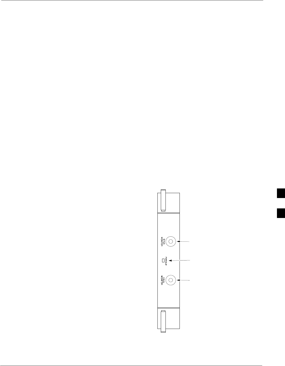
Module Front Panel LED Indicators and Connectors68P09255A69-3
Aug 2002 1X SCt4812ET Lite BTS Optimization/ATP Software Release 2.16.1.x
PRELIMINARY
6-29
CSM LED Status Combinations
PWR/ALM LED
The CSMs include on-board alarm detection. Hardware and
software/firmware alarms are indicated via the front panel indicators.
After the memory tests, the CSM loads OOS-RAM code from the Flash
EPROM, if available. If not available, the OOS-ROM code is loaded
from the Flash EPROM.
SSolid GREEN - module is INS_ACT or INS_SBY no alarm.
SSolid RED - Initial power up or module is operating in a fault (alarm)
condition.
SSlowly Flashing GREEN - OOS_ROM no alarm.
SLong RED/Short GREEN - OOS_ROM alarm.
SRapidly Flashing GREEN - OOS_RAM no alarm or
INS_ACT in DUMB mode.
SShort RED/Short GREEN - OOS_RAM alarm.
SLong GREEN/Short RED - INS_ACT or INS_SBY alarm.
SOff - no DC power or on-board fuse is open.
SSolid YELLOW - After a reset, the CSMs begin to boot. During
SRAM test and Flash EPROM code check, the LED is yellow. (If
SRAM or Flash EPROM fail, the LED changes to a solid RED and
the CSM attempts to reboot.)
Figure 6-2: CSM Front Panel Indicators & Monitor Ports
PWR/ALM
Indicator
FREQ
MONITOR
SYNC
MONITOR
FW00303
6

Module Front Panel LED Indicators and Connectors 68P09255A69-3
Aug 2002
1X SCt4812ET Lite BTS Optimization/ATP Software Release 2.16.1.x
PRELIMINARY
6-30
FREQ Monitor Connector
A test port provided at the CSM front panel via a BNC receptacle allows
monitoring of the 19.6608 MHz clock generated by the CSM. When
both CSM 1 and CSM 2 are in an in-service (INS) condition, the CSM 2
clock signal frequency is the same as that output by CSM 1.
The clock is a sine wave signal with a minimum amplitude of +2 dBm
(800 mVpp) into a 50 Ω load connected to this port.
SYNC Monitor Connector
A test port provided at the CSM front panel via a BNC receptacle allows
monitoring of the “Even Second Tick” reference signal generated by the
CSMs.
At this port, the reference signal is a Transistor-Transistor Logic (TTL)
active-high signal with a pulse width of 153 nanoseconds.
MMI Connector
Behind front panel - only accessible when card is partially extended
from SCCP shelf slot. The RS-232 MMI port connector is intended to
be used primarily in the development or factory environment, but may
be used in the field for debug/maintenance purposes.
6

Module Front Panel LED Indicators and Connectors68P09255A69-3
Aug 2002 1X SCt4812ET Lite BTS Optimization/ATP Software Release 2.16.1.x
PRELIMINARY
6-31
GLI2 LED Status Combinations
The GLI2 module indicators, controls, and connectors are described
below and shown in Figure 6-3.
The indicators and controls consist of:
SFour LEDs
SOne pushbutton
ACTIVE LED
Solid GREEN - GLI2 is active. This means that the GLI2 has shelf
control and is providing control of the digital interfaces.
Off - GLI2 is not active (i.e., Standby). The mate GLI2 should be
active.
MASTER LED
SSolid GREEN - GLI2 is Master (sometimes referred to as MGLI2).
SOff - GLI2 is non-master (i.e., Slave).
ALARM LED
SSolid RED - GLI2 is in a fault condition or in reset.
SWhile in reset transition, STATUS LED is OFF while GLI2 is
performing ROM boot (about 12 seconds for normal boot).
SWhile in reset transition, STATUS LED is ON while GLI2 is
performing RAM boot (about 4 seconds for normal boot).
SOff - No Alarm.
STATUS LED
SFlashing GREEN- GLI2 is in service (INS), in a stable operating
condition.
SOn - GLI2 is in OOS RAM state operating downloaded code.
SOff - GLI2 is in OOS ROM state operating boot code.
SPANS LED
SSolid GREEN - Span line is connected and operating.
SSolid RED - Span line is disconnected or a fault condition exists.
6

Module Front Panel LED Indicators and Connectors 68P09255A69-3
Aug 2002
1X SCt4812ET Lite BTS Optimization/ATP Software Release 2.16.1.x
PRELIMINARY
6-32
GLI2 Pushbuttons and Connectors
RESET Pushbutton - Depressing the RESET pushbutton
causes a partial reset of the CPU and a reset of all board devices.
GLI2 will be placed in the OOS_ROM state (blue).
MMI Connector - The RS-232MMI port connector is intended
primarily for development or factory use but may be used in the
field for debug/maintenance purposes.
Figure 6-3: GLI2 Front Panel Operating Indicators
MMI PORT
CONNECTOR
ACTIVE LED
STATUS RESET ALARM SPANS MASTER MMI ACTIVE
STATUS LED
RESET
PUSHBUTTON
ALARM LED
SPANS LED
MASTER LED
STATUS OFF − operating normally
ON − briefly during power−up when the Alarm LED turns OFF.
SLOW GREEN − when the GLI2 is INS (in−service)
RESET
ALARM OFF − operating normally
ON − briefly during power−up when the Alarm LED turns OFF.
SLOW GREEN − when the GLI2 is INS (in−service)
SPANS
MASTER
MMI PORT
CONNECTOR
ACTIVE
LED OPERATING STATUS
All functions on the GLI2 are reset when pressing and releasing
the switch.
ON − operating normally as active card
OFF − operating normally as standby card
Shows the operating status of the redundant cards. The redundant
card toggles automatically if the active card is removed or fails
ON − active card operating normally
OFF − standby card operating normally
The pair of GLI2 cards include a redundant status. The card in the
top shelf is designated by hardware as the active card; the card in
the bottom shelf is in the standby mode.
OFF − card is powered down, in initialization, or in standby
GREEN − operating normally
YELLOW − one or more of the equipped initialized spans is receiving
a remote alarm indication signal from the far end
RED − one or more of the equipped initialized spans is in an alarm
state
An RS−232, serial, asynchronous communications link for use as
an MMI port. This port supports 300 baud, up to a maximum of
115,200 baud communications.
FW00225
6

Module Front Panel LED Indicators and Connectors68P09255A69-3
Aug 2002 1X SCt4812ET Lite BTS Optimization/ATP Software Release 2.16.1.x
PRELIMINARY
6-33
BBX LED Status Combinations
PWR/ALM LED
The BBX2 and BBX-1X modules have their own alarm (fault) detection
circuitry that controls the state of the PWR/ALM LED.
The following list describes the states of the bi-color PWR/ALM LED
for both BBX2 and BBX-1X cards:
SSolid GREEN - INS_ACT no alarm
SSolid RED Red - initializing or power-up alarm
SSlowly Flashing GREEN - OOS_ROM no alarm
SLong RED/Short GREEN - OOS_ROM alarm
SRapidly Flashing GREEN - OOS_RAM no alarm
SShort RED/Short GREEN - OOS_RAM alarm
SLong GREEN/Short RED - INS_ACT alarm
MCC LED Status Combinations
The MCC24E and MCC-1X modules have bi-color LED indicators and
two connectors as described below. See Figure 6-4. Note that the figure
does not show the connectors because they are concealed by the
removable lens.
The LED indicators and their states are as follows:
PWR/ALM LED
SRED - fault on module
ACTIVE LED
SOff - module is inactive, off-line, or not processing traffic.
SSlowly Flashing GREEN - OOS_ROM no alarm.
SRapidly Flashing Green - OOS_RAM no alarm.
SSolid GREEN - module is INS_ACT, on-line, processing traffic.
PWR/ALM and ACTIVE LEDs
SSolid RED - module is powered but is in reset or the Board Control
Processor (BCP) is inactive.
MMI Connectors
SThe RS-232 MMI port connector (four-pin) is intended primarily for
development or factory use but may be used in the field for debugging
purposes.
SThe RJ-45 Ethernet port connector (eight-pin) is intended primarily
for development use but may be used in the field for high data rate
debugging purposes.
. . . continued on next page
6

Module Front Panel LED Indicators and Connectors 68P09255A69-3
Aug 2002
1X SCt4812ET Lite BTS Optimization/ATP Software Release 2.16.1.x
PRELIMINARY
6-34
Figure 6-4: MCC24 and MCC-1X Front Panel LEDs and LED Indications
PWR/ALM LED
LENS
(REMOVABLE)
ACTIVE LED
PWR/ALM ACTIVE
LED OPERATING STATUSCOLOR
An alarm is generated in the event of a failure
2) Continuously during fault conditions
ON - 1) Briefly during power-up
SLOW FLASHING (alternately with green) -
Concentration Highway Interface (CHI) bus
inactive on power-up
RED
RED
GREENACTIVE
PWR/ALM OFF - Operating normally
ON - Briefly during power-up and during
failure conditions
RAPIDLY FLASHING - Card is code-loaded but
not enabled
ON - Card is code-loaded and enabled (INS_ACT)
SLOW FLASHING - Card is not code-loaded
4812ETL0030-1
LPA LED Status Combinations
LPA Module LED
Each LPA module is provided with a bi-color LED on the ETIB module
next to the MMI connector. Interpret this LED as follows:
SGREEN — LPA module is active and is reporting no alarms (Normal
condition).
SFlashing GREEN/RED — LPA module is active but is reporting an
low input power condition. If no BBX is keyed, this is normal and
does not constitute a failure.
SFlashing RED — LPA is in alarm.
6

Troubleshooting: Span Control Link68P09255A69-3
Aug 2002 1X SCt4812ET Lite BTS Optimization/ATP Software Release 2.16.1.x
PRELIMINARY
6-35
Troubleshooting: Span Control Link
Span Problems (No Control Link)
Table 6-31: Troubleshoot Control Link Failure
nStep Action
1Connect the LMF computer to the MMI port on the applicable MGLI2/GLI2 as shown in
Figure 6-5.
2Start an MMI communication session with the applicable MGLI2/GLI2 by using the Windows
desktop shortcut icon (refer to Table 3-15).
3Once the connection window opens, press the LMF computer Enter key until the GLI2> prompt
is obtained.
4At the GLI2> prompt, enter:
config ni current <cr> (equivalent of span view command)
The system will respond with a display similar to the following:
The frame format in flash is set to use T1_2.
Equalization:
Span A - Default (0-131 feet for T1/J1, 120 Ohm for E1)
Span B - Default (0-131 feet for T1/J1, 120 Ohm for E1)
Span C - Default (0-131 feet for T1/J1, 120 Ohm for E1)
Span D - Default (0-131 feet for T1/J1, 120 Ohm for E1)
Span E - Default (0-131 feet for T1/J1, 120 Ohm for E1)
Span F - Default (0-131 feet for T1/J1, 120 Ohm for E1)
Linkspeed: Default (56K for T1 D4 AMI, 64K otherwise)
Currently, the link is running at the default rate
The actual rate is 0
NOTE
Defaults for span equalization are 0-131 feet for T1/J1 spans and 120 Ohm for E1.
Default linkspeed is 56K for T1 D4 AMI spans and 64K for all other types.
There is no need to change from defaults unless the OMCR/CBSC span configuration requires it.
5The span configurations loaded in the GLI must match those in the OMCR/CBSC database for the
BTS. If they do not, proceed to Table 6-32.
6Repeat steps 1 through 5 for all remaining GLIs.
7If the span settings are correct, verify the edlc parameters using the show command.
Any alarm conditions indicate that the span is not operating correctly.
STry looping back the span line from the DSX panel to the MM, and verify that the looped signal
is good.
SListen for control tone on the appropriate timeslot from the Base Site and MM.
8Exit the GLI MMI session and HyperTerminal connection by selecting File from the connection
window menu bar, and then Exit from the pull-down menu.
6
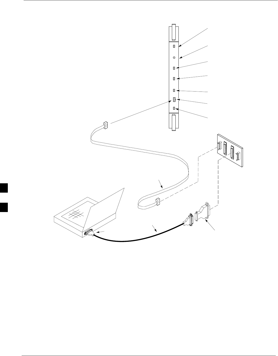
Troubleshooting: Span Control Link 68P09255A69-3
Aug 2002
1X SCt4812ET Lite BTS Optimization/ATP Software Release 2.16.1.x
PRELIMINARY
6-36
Figure 6-5: MGLI/GLI Board MMI Connection Detail
NULL MODEM
BOARD
(TRN9666A)
8-PIN TO 10-PIN
RS-232 CABLE (P/N
30-09786R01)
RS-232 CABLE
8-PIN
LMF
COMPUTER
To MMI port
DB9-TO-DB25
ADAPTER
COM1
OR
COM2
ACTIVE LED
STATUS LED
ALARM LED
MASTER LED
MMI Port
Connector
STATUS RESET ALARM SPANS MASTER MMI ACTIVE
SPANS LED
RESET
Pushbutton
6

Troubleshooting: Span Control Link68P09255A69-3
Aug 2002 1X SCt4812ET Lite BTS Optimization/ATP Software Release 2.16.1.x
PRELIMINARY
6-37
Set BTS Site Span Configuration
NOTE Perform the following procedure ONLY if span configurations
loaded in the MGLI2/GLI2s do not match those in the
OMCR/CBSC data base, AND ONLY when the exact
configuration data is available. Loading incorrect span
configuration data will render the site inoperable.
Table 6-32: Set BTS Span Parameter Configuration
nStep Action
1If not previously done, connect the LMF computer to the MMI port on the applicable
MGLI2/GLI2 as shown in Figure 6-5.
2If there is no MMI communication session in progress with the applicable MGLI2/GLI2, initiate
one by using the Windows desktop shortcut icon (refer to Table 3-15).
3At the GLI2> prompt, enter:
config ni format <option> <cr>
The terminal will display a response similar to the following:
COMMAND SYNTAX: config ni format option
Next available options:
LIST - option : Span Option
E1_1 : E1_1 - E1 HDB3 CRC4 no TS16
E1_2 : E1_2 - E1 HDB3 no CRC4 no TS16
E1_3 : E1_3 - E1 HDB3 CRC4 TS16
E1_4 : E1_4 - E1 HDB3 no CRC4 TS16
T1_1 : T1_1 - D4, AMI, No ZCS
T1_2 : T1_2 - ESF, B8ZS
J1_1 : J1_1 - ESF, B8ZS (Japan) - Default
J1_2 : J1_2 - ESF, B8ZS
T1_3 : T1_3 - D4, AMI, ZCS>
NOTE
With this command, all active (in-use) spans will be set to the same format.
4To set or change the span type, enter the correct option from the list at the entry prompt (>), as
shown in the following example:
> T1_2 <cr>
NOTE
The entry is case-sensitive and must be typed exactly as it appears in the list. If the entry is typed
incorrectly, a response similar to the following will be displayed:
CP: Invalid command
GLI2>
5An acknowledgement similar to the following will be displayed:
The value has been programmed. It will take effect after the next reset.
GLI2>
. . . continued on next page
6

Troubleshooting: Span Control Link 68P09255A69-3
Aug 2002
1X SCt4812ET Lite BTS Optimization/ATP Software Release 2.16.1.x
PRELIMINARY
6-38
Table 6-32: Set BTS Span Parameter Configuration
nActionStep
6If the current MGLI/GLI span rate must be changed, enter the following MMI command:
config ni linkspeed <cr>
The terminal will display a response similar to the following:
Next available options:
LIST - linkspeed : Span Linkspeed
56K : 56K (default for T1_1 and T1_3 systems)
64K : 64K (default for all other span configurations)
>
NOTE
With this command, all active (in-use) spans will be set to the same linkspeed.
7To set or change the span linkspeed, enter the required option from the list at the entry prompt (>),
as shown in the following example:
> 64K <cr>
NOTE
The entry is case-sensitive and must be typed exactly as it appears in the list. If the entry is typed
incorrectly, a response similar to the following will be displayed:
CP: Invalid command
GLI2>
8An acknowledgement similar to the following will be displayed:
The value has been programmed. It will take effect after the next reset.
GLI2>
9If the span equalization must be changed, enter the following MMI command:
config ni equal <cr>
The terminal will display a response similar to the following:
COMMAND SYNTAX: config ni equal span equal
Next available options:
LIST - span : Span
a : Span A
b : Span B
c : Span C
d : Span D
e : Span E
f : Span F
>
. . . continued on next page
6

Troubleshooting: Span Control Link68P09255A69-3
Aug 2002 1X SCt4812ET Lite BTS Optimization/ATP Software Release 2.16.1.x
PRELIMINARY
6-39
Table 6-32: Set BTS Span Parameter Configuration
nActionStep
10 At the entry prompt (>), enter the designator from the list for the span to be changed as shown in
the following example:
> a <cr>
The terminal will display a response similar to the following:
COMMAND SYNTAX: config ni equal a equal
Next available options:
LIST - equal : Span Equalization
0 : 0-131 feet (default for T1/J1)
1 : 132-262 feet
2 : 263-393 feet
3 : 394-524 feet
4 : 525-655 feet
5 : LONG HAUL
6 : 75 OHM
7 : 120 OHM (default for E1)
>
11 At the entry prompt (>), enter the code for the required equalization from the list as shown in the
following example:
> 0 <cr>
The terminal will display a response similar to the following:
> 0
The value has been programmed. It will take effect after the next reset.
GLI2>
12 Repeat steps 9 through 11 for each in-use span.
13 * IMPORTANT
After executing the config ni format, config ni linkspeed, and/or config ni equal
commands, the affected MGLI/GLI board MUST be reset and reloaded for changes to take effect.
Although defaults are shown, always consult site specific documentation for span type and
linkspeed used at the site.
Press the RESET button on the MGLI2/GLI2 for changes to take effect.
. . . continued on next page
6

Troubleshooting: Span Control Link 68P09255A69-3
Aug 2002
1X SCt4812ET Lite BTS Optimization/ATP Software Release 2.16.1.x
PRELIMINARY
6-40
Table 6-32: Set BTS Span Parameter Configuration
nActionStep
14 Once the MGLI/GLI has reset, execute the following command to verify span settings are as
required:
config ni current <cr> (equivalent of span view command)
The system will respond with a display similar to the following:
The frame format in flash is set to use T1_2.
Equalization:
Span A - 0-131 feet
Span B - 0-131 feet
Span C - Default (0-131 feet for T1/J1, 120 Ohm for E1)
Span D - Default (0-131 feet for T1/J1, 120 Ohm for E1)
Span E - Default (0-131 feet for T1/J1, 120 Ohm for E1)
Span F - Default (0-131 feet for T1/J1, 120 Ohm for E1)
Linkspeed: 64K
Currently, the link is running at 64K
The actual rate is 0
15 If the span configuration is not correct, perform the applicable step from this table to change it and
repeat steps 13 and 14 to verify required changes have been programmed.
16 Return to step 6 of Table 6-31.
6

Aug 2002 1X SCt4812ET Lite BTS Optimization/ATP Software Release 2.16.1.x
PRELIMINARY
A-1
Appendix A
Data Sheets
A

Optimization (Pre-ATP) Data Sheets 68P09255A69-3
Aug 2002
1X SCt4812ET Lite BTS Optimization/ATP Software Release 2.16.1.x
PRELIMINARY
A-2
Optimization (Pre-ATP) Data Sheets
Verification of Test Equipment Used
Table A-1: Verification of Test Equipment Used
Manufacturer Model Serial Number
Comments:________________________________________________________
__________________________________________________________________
A

Optimization (Pre-ATP) Data Sheets68P09255A69-3
Aug 2002 1X SCt4812ET Lite BTS Optimization/ATP Software Release 2.16.1.x
PRELIMINARY
A-3
Site Checklist
Table A-2: Site Checklist
OK Parameter Specification Comments
-Deliveries Per established procedures
-Floor Plan Verified
-
-
-
Inter Frame Cables:
Ethernet
Frame Ground
Power
Per procedure
Per procedure
Per procedure
-
-
-
Factory Data:
BBX
Test Panel
RFDS
Per procedure
Per procedure
Per procedure
-Site Temperature
-Dress Covers/Brackets
Preliminary Operations
Table A-3: Preliminary Operations
OK Parameter Specification Comments
-Frame ID DIP Switches Per site equipage
-Ethernet LAN verification Verified per procedure
Comments:_________________________________________________________
A

Optimization (Pre-ATP) Data Sheets 68P09255A69-3
Aug 2002
1X SCt4812ET Lite BTS Optimization/ATP Software Release 2.16.1.x
PRELIMINARY
A-4
Pre-Power and Initial Power Tests
Table A3a: Pre-power Checklist
OK Parameter Specification Comments
-Pre-power-up tests Table 2-3
Table 2-4
-
-
-
-
-
-
-
-
-
-
Internal Cables:
Span
CSM
Power
Ethernet Connectors
LAN A ohms
LAN B ohms
LAN A shield
LAN B shield
LAN A IN & OUT terminators
LAN B IN & OUT terminators
Ethernet Boots
verified
verified
verified
verified
verified
isolated
isolated
installed
installed
installed
-Air Impedance Cage (single cage) installed
-Initial power-up tests Table 2-4
Table 2-6
Table 2-7
-
-
Frame fans
LEDs
operational
illuminated
Comments:_________________________________________________________
A

Optimization (Pre-ATP) Data Sheets68P09255A69-3
Aug 2002 1X SCt4812ET Lite BTS Optimization/ATP Software Release 2.16.1.x
PRELIMINARY
A-5
General Optimization Checklist
Table A3b: General Optimization Checklist
OK Parameter Specification Comments
-
-
-
Preparing the LMF
Load LMF software
Create site-specific BTS directory
Create HyperTerminal connection
Table 3-1
Table 3-2
Table 3-4
-
-
-
-
LMF-to-BTS Connection
Verify GLI2 ethernet address settings
Ping LAN A
Ping LAN B
Table 3-10
Table 6-3
Table 3-16
Table 3-16
-
-
-
-
-
-
-
-
-
Verify ROM code loads for software
release
Download/Enable MGLI2
Download/Enable GLI2
Set Site Span Configuration
Set CSM clock source
Enable CSMs
Download/Enable MCCs (24/8E/1X)
Download BBXs (2 or 1X)
Program TSU NAM
Table 3-17
Table 3-18
Table 3-18
Table 6-31
Table 3-20
Table 3-21
Table 3-19
Table 3-19
Table 3-52
-
-
Test Set Calibration
Test Cable Calibration
Table 3-30
Table 3-31
Comments:_________________________________________________________
A

Optimization (Pre-ATP) Data Sheets 68P09255A69-3
Aug 2002
1X SCt4812ET Lite BTS Optimization/ATP Software Release 2.16.1.x
PRELIMINARY
A-6
GPS Receiver Operation
Table A-4: GPS Receiver Operation
OK Parameter Specification Comments
-GPS Receiver Control Task State:
tracking satellites
Verify parameter
-Initial Position Accuracy: Verify Estimated
or Surveyed
-Current Position:
lat
lon
height
RECORD in
msec and cm also
convert to deg
min sec
-Current Position: satellites tracked
Estimated:
(>4) satellites tracked,(>4) satellites visible
Surveyed:
(>1) satellite tracked,(>4) satellites visible
Verify parameter
as appropriate:
-GPS Receiver Status:Current Dilution of
Precision
(PDOP or HDOP): (<30)
Verify parameter
-Current reference source:
Number: 0; Status: Good; Valid: Yes Verify parameter
Comments:_________________________________________________________
A

Optimization (Pre-ATP) Data Sheets68P09255A69-3
Aug 2002 1X SCt4812ET Lite BTS Optimization/ATP Software Release 2.16.1.x
PRELIMINARY
A-7
LFR Receiver Operation
Table A-5: LFR Receiver Operation
OK Parameter Specification Comments
-Station call letters M X Y Z
assignment. As specified in site
documentation
-SN ratio is > 8 dB
-LFR Task State: 1fr
locked to station xxxx
Verify parameter
-Current reference source:
Number: 1; Status: Good; Valid: Yes
Verify parameter
Comments:_________________________________________________________
A

Optimization (Pre-ATP) Data Sheets 68P09255A69-3
Aug 2002
1X SCt4812ET Lite BTS Optimization/ATP Software Release 2.16.1.x
PRELIMINARY
A-8
LPA IM Reduction
Table A-6: LPA IM Reduction
Parameter Comments
CARRIER
OK LPA
#2:1
3-Sector BP
3-Sector
Specification
-1A C1 C1 No Alarms
-1B C1 C1 No Alarms
-1C C1 C1 No Alarms
-1D C1 C1 No Alarms
-3A C2 C2 No Alarms
-3B C2 C2 No Alarms
-3C C2 C2 No Alarms
-3D C2 C2 No Alarms
Comments:_________________________________________________________
A
Optimization (Pre-ATP) Data Sheets68P09255A69-3
Aug 2002 1X SCt4812ET Lite BTS Optimization/ATP Software Release 2.16.1.x
PRELIMINARY
A-9
TX Bay Level Offset / Power Output Verification for 3-Sector Configurations
1-Carrier
2-Carrier Non-adjacent Channels
Table A-7: TX BLO Calibration (3-Sector: 1-Carrier and 2-Carrier Non-adjacent Channels)
OK Parameter Specification Comments
-BBX2-1, ANT-1A = dB
BBX2-r, ANT-1A = dB
-Calibrate
carrier 1 TX Bay Level Offset = 42 dB (+5 dB)
prior to calibration
BBX2-2, ANT-2A = dB
BBX2-r, ANT-2A = dB
-BBX2-3, ANT-3A = dB
BBX2-r, ANT-3A = dB
-BBX2-4, ANT-1B = dB
BBX2-r, ANT-1B = dB
-Calibrate
carrier 2 TX Bay Level Offset = 42 dB (+5 dB)
prior to calibration
BBX2-5, ANT-2B = dB
BBX2-r, ANT-2B = dB
-BBX2-6, ANT-3B = dB
BBX2-r, ANT-3B = dB
-BBX2-1, ANT-1A = dB
BBX2-r, ANT-1A = dB
-
Calibration
Audit
carrier 1
0 dB (+0.5 dB) for gain set resolution
post-calibration
BBX2-2, ANT-2A = dB
BBX2-r, ANT-2A = dB
-
carrier 1
BBX2-3, ANT-3A = dB
BBX2-r, ANT-3A = dB
-BBX2-4, ANT-1B = dB
BBX2-r, ANT-1B = dB
-
Calibration
Audit
carrier 2
0 dB (+0.5 dB) for gain set resolution
post-calibration
BBX2-5, ANT-2B = dB
BBX2-r, ANT-2B = dB
-
carrier 2
BBX2-6, ANT-3B = dB
BBX2-r, ANT-3B = dB
Comments:________________________________________________________
__________________________________________________________________
A
Optimization (Pre-ATP) Data Sheets 68P09255A69-3
Aug 2002
1X SCt4812ET Lite BTS Optimization/ATP Software Release 2.16.1.x
PRELIMINARY
A-10
2-Carrier Adjacent Channel
Table A-8: TX Bay Level Offset Calibration (3-Sector: 2-Carrier Adjacent Channels)
OK Parameter Specification Comments
-BBX2-1, ANT-1A = dB
BBX2-r, ANT-1A = dB
-Calibrate
carrier 1 TX Bay Level Offset = 42 dB (typical),
38 dB (minimum) prior to calibration
BBX2-2, ANT-2A = dB
BBX2-r, ANT-2A = dB
-BBX2-3, ANT-3A = dB
BBX2-r, ANT-3A = dB
-BBX2-4, ANT-1B = dB
BBX2-r, ANT-1B = dB
-Calibrate
carrier 2 TX Bay Level Offset = 42 dB (typical),
38 dB (minimum) prior to calibration
BBX2-5, ANT-2B = dB
BBX2-r, ANT-2B = dB
-BBX2-6, ANT-3B = dB
BBX2-r, ANT-3B = dB
-BBX2-1, ANT-1A = dB
BBX2-r, ANT-1A = dB
-
Calibration
Audit
carrier 1
0 dB (+0.5 dB) for gain set resolution
post calibration
BBX2-2, ANT-2A = dB
BBX2-r, ANT-2A = dB
-
carrier 1
BBX2-3, ANT-3A = dB
BBX2-r, ANT-3A = dB
-BBX2-4, ANT-1B = dB
BBX2-r, ANT-1B = dB
-
Calibration
Audit
carrier 2
0 dB (+0.5 dB) for gain set resolution
post calibration
BBX2-5, ANT-2B = dB
BBX2-r, ANT-2B = dB
-
carrier 2
BBX2-6, ANT-3B = dB
BBX2-r, ANT-3B = dB
Comments:________________________________________________________
__________________________________________________________________
TX Antenna VSWR
Table A-9: TX Antenna VSWR
OK Parameter Specification Data
-VSWR -
Antenna 1A < (1.5 : 1)
-VSWR -
Antenna 2A < (1.5 : 1)
A

Optimization (Pre-ATP) Data Sheets68P09255A69-3
Aug 2002 1X SCt4812ET Lite BTS Optimization/ATP Software Release 2.16.1.x
PRELIMINARY
A-11
Table A-9: TX Antenna VSWR
OK DataSpecificationParameter
-VSWR -
Antenna 3A < (1.5 : 1)
-VSWR -
Antenna 1B < (1.5 : 1)
-VSWR -
Antenna 2B < (1.5 : 1)
-VSWR -
Antenna 3B < (1.5 : 1)
Comments:________________________________________________________
__________________________________________________________________
A

Optimization (Pre-ATP) Data Sheets 68P09255A69-3
Aug 2002
1X SCt4812ET Lite BTS Optimization/ATP Software Release 2.16.1.x
PRELIMINARY
A-12
RX Antenna VSWR
Table A-10: RX Antenna VSWR
OK Parameter Specification Data
-VSWR -
Antenna 1A < (1.5 : 1)
-VSWR -
Antenna 2A < (1.5 : 1)
-VSWR -
Antenna 3A < (1.5 : 1)
-VSWR -
Antenna 1B < (1.5 : 1)
-VSWR -
Antenna 2B < (1.5 : 1)
-VSWR -
Antenna 3B < (1.5 : 1)
Comments:_________________________________________________________
Alarm Verification
Table A-11: CDI Alarm Input Verification
OK Parameter Specification Data
-
Verify CDI alarm input
operation per Table 3-6. BTS Relay #XX -
Contact Alarm
Sets/Clears
Comments:_________________________________________________________
A

Site Serial Number Check List68P09255A69-3
Aug 2002 1X SCt4812ET Lite BTS Optimization/ATP Software Release 2.16.1.x
PRELIMINARY
A-13
Site Serial Number Check List
Date Site
SCCP Shelf
NOTE: For BBXs and MCCs, enter the type as well as serial number;
for example, BBX2, BBX-1X, MCC8, MCC24, MCC-1X.
Site I/O A & B
SCCP Shelf
CSM-1
CSM-2
HSO/LFR
CCD-1
CCD-2
AMR-1
AMR-2
MPC-1
MPC-2
Fans 1-2
GLI2-1
GLI2-2
BBX-1
BBX-2
BBX-3
BBX-4
BBX-5
BBX-6
BBX-R1
MCC-1
MCC-2
MCC-3
MCC-4
CIO
SWITCH
PS-1
PS-2
A

Site Serial Number Check List 68P09255A69-3
Aug 2002
1X SCt4812ET Lite BTS Optimization/ATP Software Release 2.16.1.x
PRELIMINARY
A-14
LPAs
LPA 1A
LPA 1B
LPA 1C
LPA 1D
LPA 3A
LPA 3B
LPA 3C
LPA 3D
A

Aug 2002 1X SCt4812ET Lite BTS Optimization/ATP Software Release 2.16.1.x
PRELIMINARY
B-1
Appendix B
FRU Optimization/ATP Test Matrix
B

FRU Optimization/ATP Test Matrix 68P09255A69-3
Aug 2002
1X SCt4812ET Lite BTS Optimization/ATP Software Release 2.16.1.x
PRELIMINARY
B-2
FRU Optimization/ATP Test Matrix
Usage & Background
Periodic maintenance of a site may also mandate re-optimization of
specific portions of the site. An outline of some basic guidelines is
included in the following tables.
NOTE Re-optimization steps listed for any assembly detailed in the
tables below must be performed anytime an RF cable associated
with it is replaced.
Detailed Optimization/ATP Test Matrix
Table B-1 outlines in more detail the tests that would need to be
performed if one of the BTS components were to fail and be replaced. It
is also assumes that all modules are placed OOS-ROM via the LMF
until full redundancy of all applicable modules is implemented.
The following guidelines should also be noted when using this table:
NOTE Not every procedure required to bring the site back in service is
indicated in Table B-1. It is meant to be used as a guideline
ONLY. The table assumes that the user is familiar enough with
the BTS Optimization/ATP procedure to understand which test
equipment set ups, calibrations, and BTS site preparation will be
required before performing the Table # procedures referenced.
Passive BTS components (such as the bandpass filters and 2:1
combiners) only require a TX calibration audit to be performed in lieu of
a full path calibration. If the TX path calibration audit fails, the entire RF
path calibration will need to be repeated. If the RF path calibration fails,
further troubleshooting is warranted.
NOTE If any significant change in signal level results from any
component being replaced in the RX or TX signal flow paths, it
would be identified by re-running the RX and TX calibration
audit command.
When the CIO is replaced, the SCCP shelf remains powered up. The
BBX boards may need to be removed, then re-installed into their
original slots, and re-downloaded (code and BLO data). RX and TX
calibration audits should then be performed on the affected carrier
sectors.
B

FRU Optimization/ATP Test Matrix68P09255A69-3
Aug 2002 1X SCt4812ET Lite BTS Optimization/ATP Software Release 2.16.1.x
PRELIMINARY
B-3
Table B-1: SC 4812ET Lite BTS Optimization and ATP Test Matrix
Doc
Tbl
#Description
DRDC or TRDC
RX Cables
TX Cables
MPC / EMPC
CIO
SCCP Shelf Assembly (Backplane)
BBX2/BBX-1X
MCC24E/MCC8E/MCC-1X
CSM/GPS
LFR
HSO/HSOX
50-pair Punchblock (with RGPS)
RGD/20-pair Punchblock with RGD
CCD Card
GLI2
ETIB or Associated Cables
LPAC Cable
LPA or LPA Trunking Module
LPA Bandpass Filter or Combiner
Switch Card
RFDS Cables
RFDS
Table 3-18/
Table 3-19/ Download Code/Data D D D D D D
Table 3-21 Enable CSMs D D D D 9
Table 3-24 GPS & HSO Initialization
/ Verification D DDDDDD 9
Table 3-25 LFR Initialization /
Verification D D D
Table 3-41 TX Path Calibration 4 4 1 1 4 * 3 3 4 7
Table 3-42 Download Offsets to
BBX 4 1 4 *
Table 3-43 TX Path Audit 4 4 1 1 4 * 3 4 7
Table 3-51 RFDS Path Calibration
and Offset Data
Download 65451 1 6 * 3 46 6
Table 4-8 Spectral Purity TX Mask 4 1 4 * * * *
Table 4-9 Waveform Quality (rho) 4 * 1 4 * ** 10 * *
Table 4-10 Pilot Time Offset 4 * 1 4 * ** * *
Table 4-11 Code Domain Power /
Noise Floor 4 1 4 8 8 8 8 * * *
Table 4-12 FER Test 5 5 5 2 2 5 8 8 8 8 * 7
Table 3-54
through
Table 3-63 Alarm Tests D
. . . continued on next page
B

FRU Optimization/ATP Test Matrix 68P09255A69-3
Aug 2002
1X SCt4812ET Lite BTS Optimization/ATP Software Release 2.16.1.x
PRELIMINARY
B-4
Table B-1: SC 4812ET Lite BTS Optimization and ATP Test Matrix
Doc
Tbl
#
RFDS
RFDS Cables
Switch Card
LPA Bandpass Filter or Combiner
LPA or LPA Trunking Module
LPAC Cable
ETIB or Associated Cables
GLI2
CCD Card
RGD/20-pair Punchblock with RGD
50-pair Punchblock (with RGPS)
HSO/HSOX
LFR
CSM/GPS
MCC24E/MCC8E/MCC-1X
BBX2/BBX-1X
SCCP Shelf Assembly (Backplane)
CIO
MPC / EMPC
TX Cables
RX Cables
DRDC or TRDC
Description
OPTIMIZATION AND TEST LEGEND:
D Required
* Perform if determined necessary for addtional fault isolation, repair assurance, or required for site
certification.
1. Perform on all carrier and sector TX paths to the SCCP cage.
2. Perform on all carrier and sector main and diversity RX paths to the SCCP cage.
3. Perform on all primary and redundant TX paths of the affected carrier. (LPAC replacement affects
all carriers.)
4. Perform on the affected carrier and sector TX path(s) (BBXR replacement affects all carrier and
sector TX paths).
5. Perform on the affected carrier and sector RX path(s) (BBXR replacement affects all carrier RX
paths).
6. Perform on all RF paths of the affected carrier and sector (RFDS replacement affects all
carriers).
7. Perform with redundant BBX for at least one sector on one carrier.
8. Verify performance by performing on one sector of one carrier only.
9. Perform only if RGD/RGPS, LFR antenna, or HSO or LFR expansion was installed.
10. Verify performance by performing testing on one sector of each carrier.
B

Aug 2002 1X SCt4812ET Lite BTS Optimization/ATP Software Release 2.16.1.x
PRELIMINARY
C-1
Appendix C
BBX Gain Set Point vs. BTS Output
C

BBX Gain Set Point vs. BTS Output 68P09255A69-3
Aug 2002
1X SCt4812ET Lite BTS Optimization/ATP Software Release 2.16.1.x
PRELIMINARY
C-2
BBX Gain Set Point vs. BTS Output
Usage & Background
Table C-1 outlines the relationship between the total of all code domain
channel element gain settings (digital root sum of the squares) and the
BBX Gain Set Point between 33.0 dBm and 44.0 dBm. The resultant
RF output (as measured in dBm at the BTS antenna connector) is shown
in the table. The table assumes that the BBX Bay Level Offset (BLO)
values have been calculated.
As an illustration, consider a BBX keyed up to produce a CDMA carrier
with only the Pilot channel (no MCCs forward link enabled). Pilot gain
is set to 262. In this case, the BBX Gain Set Point is shown to correlate
exactly to the actual RF output anywhere in the 33 to 44 dBm output
range. (This is the level used to calibrate the BTS).
Table C-1: BBX Gain Set Point vs. Actual BTS Output (in dBm)
dBm'
Gainb
44 43 42 41 40 39 38 37 36 35 34 33
541 - - - - - - - 43.3 42.3 41.3 40.3 39.3
533 - - - - - - - 43.2 42.2 41.2 40.2 39.2
525 - - - - - - - 43 42 41 40 39
517 - - - - - - - 42.9 41.9 40.9 39.9 38.9
509 - - - - - - - 42.8 41.8 40.8 39.8 38.8
501 - - - - - - - 42.6 41.6 40.6 39.6 38.6
493 - - - - - - 43.5 42.5 41.5 40.5 39.5 38.5
485 - - - - - - 43.4 42.4 41.4 40.4 39.4 38.4
477 - - - - - - 43.2 42.2 41.2 40.2 39.2 38.2
469 - - - - - - 43.1 42.1 41.1 40.1 39.1 38.1
461 - - - - - - 42.9 41.9 40.9 39.9 38.9 37.9
453 - - - - - - 42.8 41.8 40.8 39.8 38.8 37.8
445 - - - - - 43.6 42.6 41.6 40.6 39.6 38.6 37.6
437 - - - - - 43.4 42.4 41.4 40.4 39.4 38.4 37.4
429 - - - - - 43.3 42.3 41.3 40.3 39.3 38.3 37.3
421 - - - - - 43.1 42.1 41.1 40.1 39.1 38.1 37.1
413 - - - - - 43 42 41 40 39 38 37
405 - - - - - 42.8 41.8 40.8 39.8 38.8 37.8 36.8
397 - - - - 43.6 42.6 41.6 40.6 39.6 38.6 37.6 36.6
389 - - - - 43.4 42.4 41.4 40.4 39.4 38.4 37.4 36.4
. . . continued on next page
C

BBX Gain Set Point vs. BTS Output68P09255A69-3
Aug 2002 1X SCt4812ET Lite BTS Optimization/ATP Software Release 2.16.1.x
PRELIMINARY
C-3
Table C-1: BBX Gain Set Point vs. Actual BTS Output (in dBm)
dBm'
Gainb
333435363738394041424344
381 - - - - 43.3 42.3 41.3 40.3 39.3 38.3 37.3 36.3
374 - - - - 43.1 42.1 41.1 40.1 39.1 38.1 37.1 36.1
366 - - - - 42.9 41.9 40.9 39.9 38.9 37.9 36.9 35.9
358 - - - - 42.7 41.7 40.7 39.7 38.7 37.7 36.7 35.7
350 - - - 43.5 42.5 41.5 40.5 39.5 38.5 37.5 36.5 35.5
342 - - - 43.3 42.3 41.3 40.3 39.3 38.3 37.3 36.3 35.3
334 - - - 43.1 42.1 41.1 40.1 39.1 38.1 37.1 36.1 35.1
326 - - - 42.9 41.9 40.9 39.9 38.9 37.9 36.9 35.9 34.9
318 - - - 42.7 41.7 40.7 39.7 38.7 37.7 36.7 35.7 34.7
310 - - 43.5 42.5 41.5 40.5 39.5 38.5 37.5 36.5 35.5 34.5
302 - - 43.2 42.2 41.2 40.2 39.2 38.2 37.2 36.2 35.2 34.2
294 - - 43 42 41 40 39 38 37 36 35 34
286 - - 42.8 41.8 40.8 39.8 38.8 37.8 36.8 35.8 34.8 33.8
278 - 43.5 42.5 41.5 40.5 39.5 38.5 37.5 36.5 35.5 34.5 33.5
270 - 43.3 42.3 41.3 40.3 39.3 38.3 37.3 36.3 35.3 34.3 33.3
262 - 43 42 41 40 39 38 37 36 35 34 33
254 - 42.7 41.7 40.7 39.7 38.7 37.7 36.7 35.7 34.7 33.7 32.7
246 43.4 42.4 41.4 40.4 39.4 38.4 37.4 36.4 35.4 34.4 33.4 32.4
238 43.2 42.2 41.2 40.2 39.2 38.2 37.2 36.2 35.2 34.2 33.2 32.2
230 42.9 41.9 40.9 39.9 38.9 37.9 36.9 35.9 34.9 33.9 32.9 31.9
222 42.6 41.6 40.6 39.6 38.6 37.6 36.6 35.6 34.6 33.6 32.6 31.6
214 42.2 41.2 40.2 39.2 38.2 37.2 36.2 35.2 34.2 33.2 32.2 31.2
C

BBX Gain Set Point vs. BTS Output 68P09255A69-3
Aug 2002
1X SCt4812ET Lite BTS Optimization/ATP Software Release 2.16.1.x
PRELIMINARY
C-4
Notes
C

Aug 2002 1X SCt4812ET Lite BTS Optimization/ATP Software Release 2.16.1.x
PRELIMINARY
D-1
Appendix D
CDMA Operating Frequency
Information
D

CDMA Operating Frequency Programming Information 68P09255A69-3
Aug 2002
1X SCt4812ET Lite BTS Optimization/ATP Software Release 2.16.1.x
PRELIMINARY
D-2
CDMA Operating Frequency Programming Information
Introduction
Programming of each of the BTS BBX synthesizers is performed by the
BTS GLI2s via the Concentration Highway Interface (CHI) bus. This
programming data determines the transmit and receive transceiver
operating frequencies (channels) for each BBX.
1900 MHz PCS Channels
Figure D-1 shows the valid channels for the North American PCS
1900 MHz frequency spectrum. There are 10 CDMA wireline or
non-wireline band channels used in a CDMA system (unique per
customer operating system).
Figure D-1: North America PCS Frequency Spectrum (CDMA Allocation)
FREQ (MHz)
RX TX
275
1175
CHANNEL
1863.75
925
1851.2525
1871.25425
675 1883.75
1896.25
1908.75
1943.75
1931.25
1951.25
1963.75
1976.25
1988.75
A
D
B
E
F
C
FW00463
D