Nokia Solutions and Networks T5CT1 Cellular CDMA base station User Manual IHET5CT1 GLI2 Manual 2 of 6
Nokia Solutions and Networks Cellular CDMA base station IHET5CT1 GLI2 Manual 2 of 6
Contents
- 1. IHET5CT1 GLI2 Manual 1 of 6
- 2. IHET5CT1 GLI2 Manual 2 of 6
- 3. IHET5CT1 GLI2 Manual 3 of 6
- 4. IHET5CT1 GLI2 Manual 4 of 6
- 5. IHET5CT1 GLI2 Manual 5 of 6
- 6. IHET5CT1 GLI2 Manual 6 of 6
- 7. IHET5CT1 GLI3 Manual 1 of 6
- 8. IHET5CT1 GLI3 Manual 4 of 6
- 9. IHET5CT1 GLI3 Manual 5 of 6
- 10. IHET5CT1 GLI3 Manual 6 of 6
IHET5CT1 GLI2 Manual 2 of 6

BTS Equipment Identification – continued
SCt4812ET BTS Optimization/ATP — CDMA LMF Jan 2002
1-26
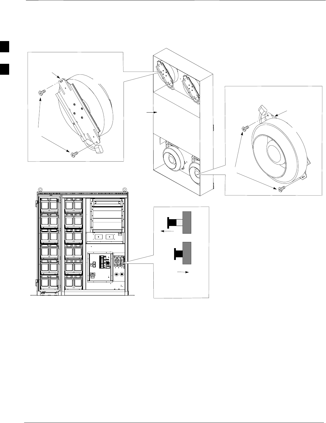
Battery Compartment Fan
The battery compartment fan provides air circulation for the two battery
compartments. It is located on the inside of the battery compartment
door.
Heat Exchanger
The Heat Exchanger provides cooling to the rectifier compartment of the
Power Cabinet. The Heat Exchanger is located in the primary front door
of the Power Cabinet.
Rectifiers
The +27 Vdc rectifiers convert the AC power supplied to the Power
Cabinet to +27 Vdc to power the RF Cabinet and maintain the charge of
the batteries.
AC Load Center
The ACLC is the point of entry for AC Power to the Power Cabinet. It
incorporates AC power distribution and surge protection.
Punch Block
The Punch Block is the interface for the alarm signalling between the
Power Cabinet and the RF Cabinet.
1

Jan 2002 SCt4812ET BTS Optimization/ATP — CDMA LMF
Chapter 2: Preliminary Operations
Table of Contents
Preliminary Operations: Overview 2-1. . . . . . . . . . . . . . . . . . . . . . . . . . . . . . . . . . .
Introduction 2-1. . . . . . . . . . . . . . . . . . . . . . . . . . . . . . . . . . . . . . . . . . . . . .
Cellsite Types 2-1. . . . . . . . . . . . . . . . . . . . . . . . . . . . . . . . . . . . . . . . . . . . .
CDF 2-1. . . . . . . . . . . . . . . . . . . . . . . . . . . . . . . . . . . . . . . . . . . . . . . . . . . .
Site Equipage Verification 2-1. . . . . . . . . . . . . . . . . . . . . . . . . . . . . . . . . . .
Initial Installation of Boards/Modules 2-1. . . . . . . . . . . . . . . . . . . . . . . . . .
Setting Frame C–CCP Shelf Configuration Switch 2-2. . . . . . . . . . . . . . .
Initial Power Up 2-3. . . . . . . . . . . . . . . . . . . . . . . . . . . . . . . . . . . . . . . . . . . . . . . . .
Introduction 2-3. . . . . . . . . . . . . . . . . . . . . . . . . . . . . . . . . . . . . . . . . . . . . .
Required Tools 2-3. . . . . . . . . . . . . . . . . . . . . . . . . . . . . . . . . . . . . . . . . . . .
Cabling Inspection 2-3. . . . . . . . . . . . . . . . . . . . . . . . . . . . . . . . . . . . . . . . .
Initial Inspection and Setup 2-3. . . . . . . . . . . . . . . . . . . . . . . . . . . . . . . . . .
Power Up Sequence 2-4. . . . . . . . . . . . . . . . . . . . . . . . . . . . . . . . . . . . . . . .
Applying AC Power 2-5. . . . . . . . . . . . . . . . . . . . . . . . . . . . . . . . . . . . . . .
Power Cabinet Power Up Tests 2-6. . . . . . . . . . . . . . . . . . . . . . . . . . . . . . .
DC Power Pre-test (BTS Frame) 2-7. . . . . . . . . . . . . . . . . . . . . . . . . . . . . .
RF Cabinet Power Up 2-8. . . . . . . . . . . . . . . . . . . . . . . . . . . . . . . . . . . . . .
Battery Charge Test (Connected Batteries) 2-10. . . . . . . . . . . . . . . . . . . . . .
Battery Discharge Test 2-10. . . . . . . . . . . . . . . . . . . . . . . . . . . . . . . . . . . . . .
Heat Exchanger Power Up 2-11. . . . . . . . . . . . . . . . . . . . . . . . . . . . . . . . . . .
2

Table of Contents – continued
SCt4812ET BTS Optimization/ATP — CDMA LMF Jan 2002
Notes
2
Preliminary Operations: Overview
Jan 2002 2-1
SCt4812ET BTS Optimization/ATP — CDMA LMF
Introduction
This section first verifies proper frame equipage. This includes verifying
module placement, jumper, and dual in–line package (DIP) switch
settings against the site-specific documentation supplied for each BTS
application. Next, pre-power up and initial power-up procedures are
presented.
Cellsite Types
Sites are configured as with a maximum of 4 carriers, 3–sectored with a
maximum of 4 carriers, and 6–sectored with a maximum of 2 carriers.
Each type has unique characteristics and must be optimized accordingly.
CDF
The Cell-site Data File (CDF) contains site type and equipage data
information and passes it directly to the LMF during optimization. The
number of modem frames, C–CCP shelves, BBX and MCC boards (per
cage), and linear power amplifier assignments are some of the equipage
data included in the CDF.
Site Equipage Verification
Review the site documentation. Match the site engineering equipage data
to the actual boards and modules shipped to the site. Physically inspect
and verify the equipment provided for the BTS or Modem frame and
ancillary equipment frame.
Always wear a conductive, high impedance wrist strap
while handling any circuit card/module to prevent damage
by ESD. After removal, the card/module should be placed
on a conductive surface or back into the anti–static bag it
was shipped in.
CAUTION
Initial Installation of
Boards/Modules
Table 2-1: Initial Installation of Boards/Modules
Step Action
1Refer to the site documentation and install all boards and modules into the appropriate shelves as
required. Verify they are NOT SEATED at this time.
2As the actual site hardware is installed, record the serial number of each module on a “Serial Number
Checklist” in the site logbook.
2
Preliminary Operations: Overview – continued
SCt4812ET BTS Optimization/ATP — CDMA LMF Jan 2002
2-2
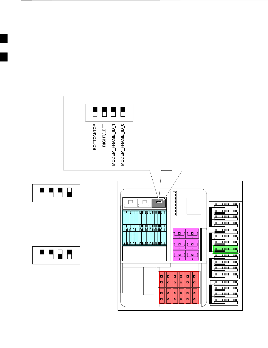
Setting Frame C–CCP Shelf
Configuration Switch
If the frame is a Starter BTS, the backplane switch settings behind the
fan module should be set to the ON position (see Figure 2-1).
The switch setting must be verified and set before power is applied to the
BTS equipment.
SC 4812ET
C–CCP SHELF
FAN MODULE
REMOVED
5 RU RACK SPACE
RFDS
EBA
ETIB
ON
OFF STARTER FRAME
Figure 2-1: Backplane DIP Switch Settings
FW00167
ON
OFF
EXPANSION
FRAME 1
SETTING
ON
OFF
EXPANSION
FRAME 2
SETTING
BOTTOM / TOP
RIGHT / LEFT
MODEM_FRAME_ID_1
MODEM_FRAME_ID_0
BOTTOM / TOP
RIGHT / LEFT
MODEM_FRAME_ID_1
MODEM_FRAME_ID_0
2
Initial Power Up
Jan 2002 2-3
SCt4812ET BTS Optimization/ATP — CDMA LMF
Introduction
The following information is used to check for any electrical short
circuits and to verify the operation and tolerances of the cellsite and BTS
power supply units before applying power for the first time. It contains
instructional information on the initial proper power up procedures for
the SC 4812ET power cabinet and RF cabinet. Also presented are tests
to be preformed on the power cabinet. Please pay attention to all
cautions and warning statements in order to prevent accidental injury to
personnel.
Required Tools
The following tools are used in the procedures.
SDC current clamp (600 Amp capability with jaw size to accommodate
2/0 cable).
SHot Air Gun – (optional for part of the Alarm Verification)
SDigital Multimeter (DMM)
Cabling Inspection
Using the site-specific documentation generated by Motorola Systems
Engineering, verify that the following cable systems are properly
connected:
SReceive RF cabling – up to 12 RX cables
STransmit RF cabling – up to six TX cables
For positive power applications (+27 V):
SThe positive power cable is red.
SThe negative power cable is black. (The black power
cable is at ground potential.)
IMPORTANT
*
Initial Inspection and Setup
Ensure all battery breakers for unused battery positions are
open (pulled out) during any part of the power up process,
and remain in the off position when leaving the site.
CAUTION
Table 2-2: Initial Inspection and Setup
Step Action
1Verify that ALL AC and DC breakers are turned OFF in both the Power and RF cabinets. Verify that
the DC power cables between the Power and RF cabinets are connected with the correct polarity
2The RED cables connect to the uppermost three (3) terminals (marked +) in both cabinets. Confirm
that the split phase 240/120 AC supply is correctly connected to the AC load center input.
2
Initial Power Up – continued
SCt4812ET BTS Optimization/ATP — CDMA LMF Jan 2002
2-4
Failure to connect the proper AC feed will damage the
surge protection module inside the AC load center.
CAUTION
Power Up Sequence
The first task in the power up sequence is to apply AC power to the
Power cabinet. Once power is applied a series of AC Voltage
measurements is required.
Table 2-3: AC Voltage Measurements
Step Action
1Measure the AC voltages connected to the AC load center (access the terminals from the rear of the
cabinet after removing the AC load center rear panel). See Figure 2-2.
2Measure the AC voltage from terminal L1 to neutral. This voltage should be in the range of nominally
115 to 120 Vac.
3Measure the AC voltage from terminal L1 to ground. This voltage should be in the range of nominally
115 to 120 Vac.
4Measure the AC voltage from terminal L2 to neutral. This voltage should be in the range of nominally
115 to 120 Vac.
5Measure the AC voltage from terminal L2 to ground. This voltage should be in the range of nominally
115 to 120 Vac.
6Measure L1 – L2 – should be from 208 to 240 Vac.
If the AC voltages are in excess of 120 V (or exceed
200 V) when measuring between terminals L1 or L2 to
neutral or ground, STOP and Do Not proceed until the
cause of the higher voltages are determined. The power
cabinet WILL be damaged if the Main breaker is turned
on with excessive voltage on the inputs.
CAUTION
2
Initial Power Up – continued
Jan 2002 2-5
SCt4812ET BTS Optimization/ATP — CDMA LMF
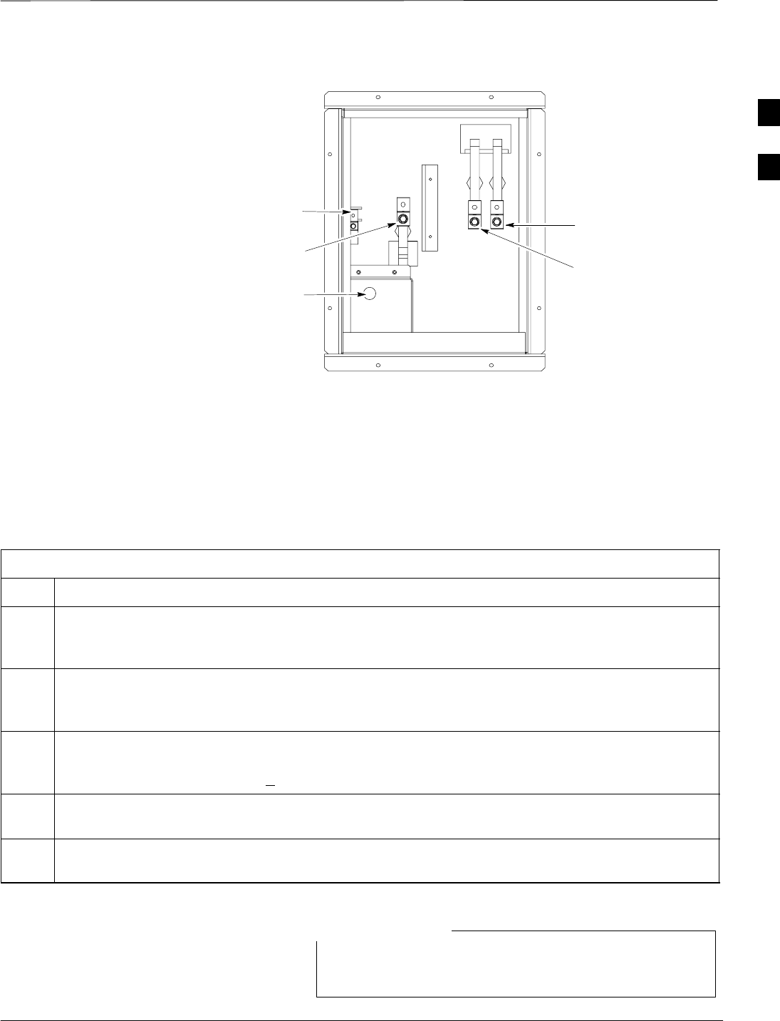
Figure 2-2: AC Load Center Wiring
G= Ground
N = Neutral
L1 = Line 1
L2 = Line 2
G
N
AC to Pilot Beacon
L2
L1
FW00305
Applying AC Power
Once AC Voltage Measurements are complete, apply AC power to the
Power Cabinet. Table 2-4 provides the procedure for applying AC
power.
Table 2-4: Applying AC Power
Step Action
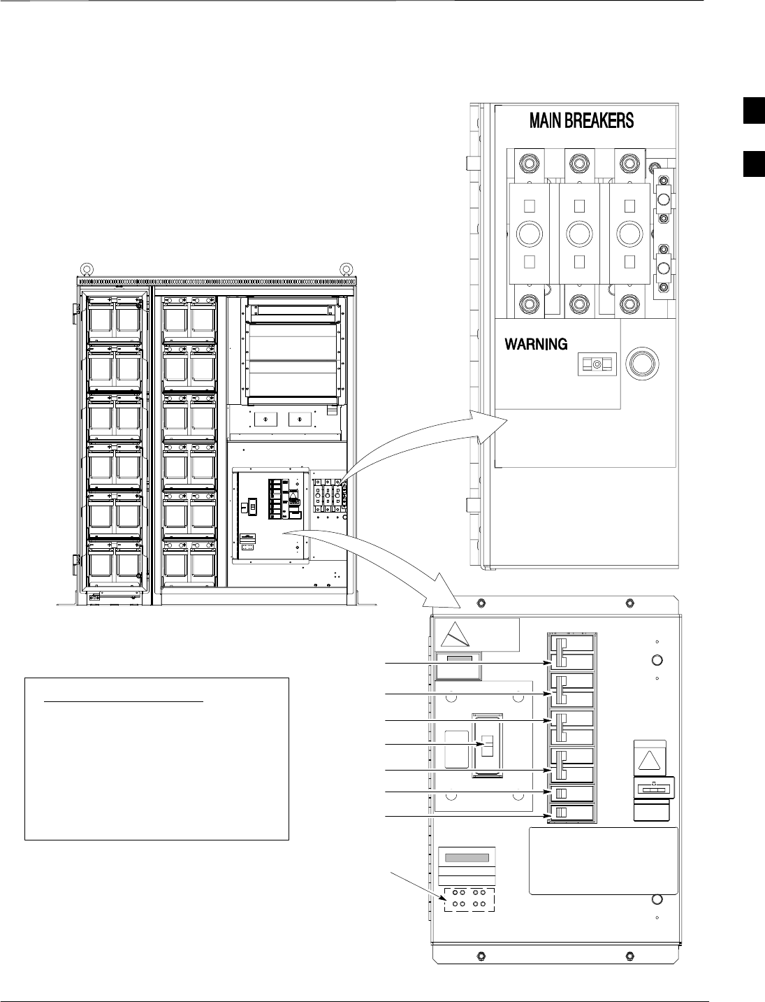
1When the input voltages are verified as correct, turn the Main AC breaker (located on the front of the
ACLC) ON. Observe that all eight (8) green LEDs on the front of the ACLC are illuminated (see
Figure 2-7).
2Turn Rectifier 1 and Rectifier 2 AC branch breakers (on the AC Load Center) ON. All the installed
rectifier modules (see Figure 2-7) will start up and should each have two green LEDs (DC and Power)
illuminated.
3Turn the Meter Alarm Panel module, ON (see Figure 2-3), while observing the K2 contact in the
PDA assembly (see Figure 2-9). The contact should close. The Meter Alarm Panel voltage meter
should read approximately 27.4 + 0.2 Vdc.
4Turn the Temperature Compensation Panel (TCP) ON, (see Figure 2-4). Verify that the Meter Alarm
Control Panel does not have any alarm LEDs illuminated.
5Check the rectifier current bargraph displays (green LED display on the rectifier module). None
should be illuminated at this point.
If batteries are fitted, turn on the two battery heater AC
breakers on the AC Load Center.
NOTE
2
Initial Power Up – continued
SCt4812ET BTS Optimization/ATP — CDMA LMF Jan 2002
2-6
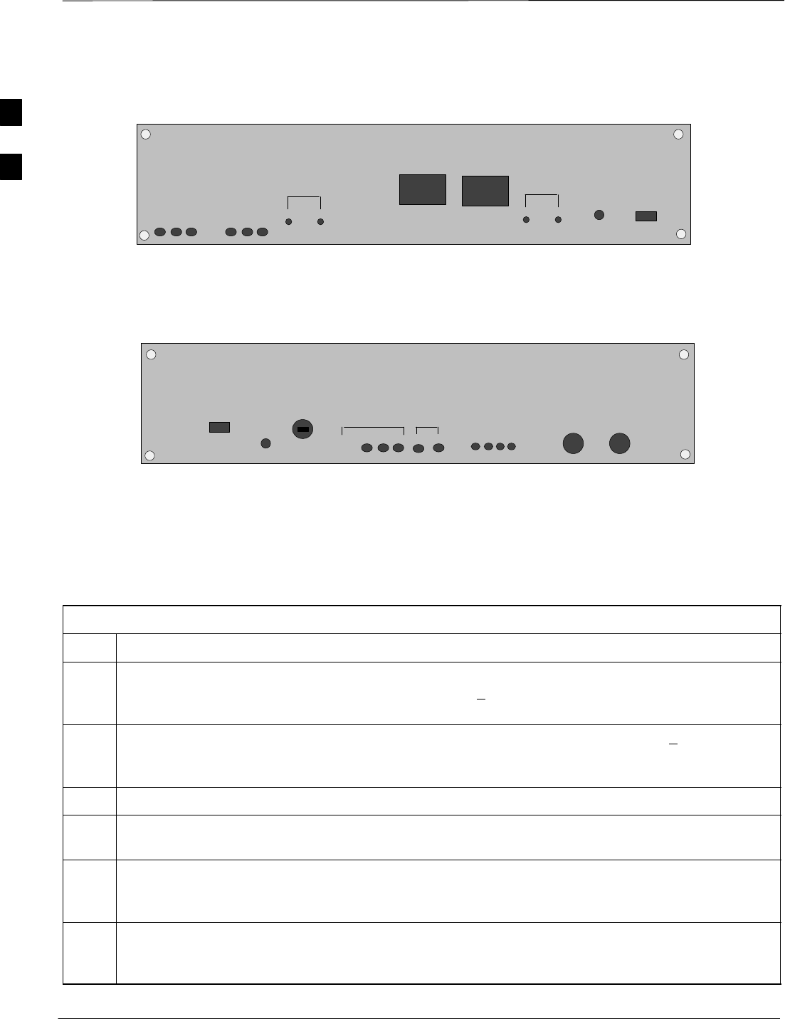
Figure 2-3: Meter Alarm Panel
OFF
VOLT
VOLT
–
+
TEST POINTS
AMPS
–
+
TEST POINTS
AMP
PWR
ON
FRONT VIEW FW00245
Figure 2-4: Temperature Compensation Panel
OFF
V ADJ
SENSOR 25_ c
SENSE
–
+
COM
ON
ON
FRONT VIEW
1/2 A 250V
12
TEMPERATURE COMPENSATION PANEL
FW00246
Power Cabinet Power Up
Tests
Table 2-5 lists the step–by–step instructions for Power Up Tests.
Table 2-5: Power Cabinet Power Up Tests
Step Action
1Probe the output voltage test point on the Meter Alarm Panel while pressing the 25° C set button on
the TCP (see Figure 2-4). The voltage should read 27.4 + 0.2 Vdc. Adjust Master Voltage on Meter
Alarm Panel if necessary. Release the TCP 25° C set button.
2Depending on the ambient temperature, the voltage reading may now change by up to + 1.5 V
compared to the reading just measured. If it is cooler than 25_C, the voltage will be higher, and if it is
warmer than 25_C, the voltage will be lower.
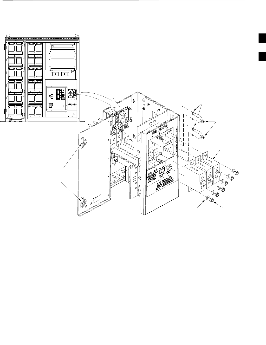
3Ensure the RF cabinet 400A main DC breaker is OFF.
4Close the three (3) Main DC breakers on the Power Cabinet ONLY. Close by holding in the reset
button on the front of the PDA, and engaging one breaker at a time.
5Measure the voltage between the + and – terminals at the rear of the Power Cabinet and the RF
Cabinet, observing that the polarity is correct. The voltage should be the same as the measurement in
step 2.
6Place the probes across the black and red battery buss bars in each battery compartment. Place the
probe at the bottom of the buss bars where the cables are connected. The DC voltage should measure
the same as the previous step.
2

Initial Power Up – continued
Jan 2002 2-7
SCt4812ET BTS Optimization/ATP — CDMA LMF
DC Power Pre-test (BTS Frame) Before applying any power to the BTS cabinet, verify there are no shorts
in the RF or power DC distribution system (see Figure 2-5).
Table 2-6: DC Power Pre–test (BTS Frame)
Step Action
1Physically verify that all AC rectifiers supplying power to the RF cabinets are OFF or disabled (see
Figure 2-5). There should be no 27 Vdc on DC feed terminals.
2On each RF cabinet:
SUnseat all circuit boards/ modules in the distribution shelf, transceiver shelf, and Single Carrier
Linear Power Amplifier (SCLPA) shelves, but leave them in their associated slots.
SUnseat all circuit boards (except CCD and CIO cards) in the C–CCP shelf and LPA shelves, but
leave them in their associated slots.
SSet C–CCP shelf breakers to the OFF position by pulling out power distribution breakers (labeled
C–CCP 1, 2, 3 – located on the power distribution panel).
SSet LPA breakers to the OFF position by pulling out power distribution breakers (8 breakers,
labeled 1A–1B through 4C–4D – located on the power distribution panel).
3Verify that the resistance from the power (+) feed terminals with respect to the ground terminal on the
cabinet measures > 500 Ω (see Figure 2-5).
SIf reading is < 500 Ω, a short may exist somewhere in the DC distribution path supplied by the
breaker. Isolate the problem before proceeding. A reading > 3 MΩ could indicate an open (or
missing) bleeder resistor (installed across the filter capacitors behind the breaker panel).
4Set the 400 Amp Main Breaker and the C–CCP breakers (C–CCP 1, 2, 3) to the ON position by
pushing them IN one at a time. Repeat step 3 after turning on each breaker.
* IMPORTANT
If, after inserting any board/module, the ohmmeter stays at 0 Ω, a short probably exists in that
board/module. Replace the suspect board/module and repeat the test. If test still fails, isolate the
problem before proceeding.
5Insert and lock the DC/DC converter modules into their associated slots one at a time. Repeat step3
after inserting each module.
SA typical response is that the ohmmeter will steadily climb in resistance as capacitors charge, finally
indicating approximately 500 Ω.
! CAUTION
Verify the correct power/converter modules by observing the locking/retracting tabs appear as follows:
–
6Insert and lock all remaining circuit boards and modules into their associated slots in the C–CCP shelf.
Repeat step 3 after inserting and locking each board or module.
SA typical response is that the ohmmeter will steadily climb in resistance as capacitors charge,
stopping at approximately 500 Ω..
. . . continued on next page
2

Initial Power Up – continued
SCt4812ET BTS Optimization/ATP — CDMA LMF Jan 2002
2-8
Table 2-6: DC Power Pre–test (BTS Frame)
Step Action
7Set the 8 LPA breakers ON by pushing them IN one at a time. Repeat step 3 after turning on each
breaker.
SA typical response is that the ohmmeter will steadily climb in resistance as capacitors charge,
stopping at approximately 500 Ω..
8Seat all LPA and associated LPA fan modules into their associated slots in the shelves one at a time.
Repeat step 3 after seating each LPA and associated LPA fan module.
SA typical response is that the ohmmeter will steadily climb in resistance as capacitors charge,
stopping at approximately 500 Ω..
9Seat the Heat Exchanger, ETIB, and Options breakers one at a time. Repeat step 3.
RF Cabinet Power Up
Table 2-7 covers the procedures for properly powering up the RF
Cabinet.
Table 2-7: RF Cabinet Power Up
Step Action
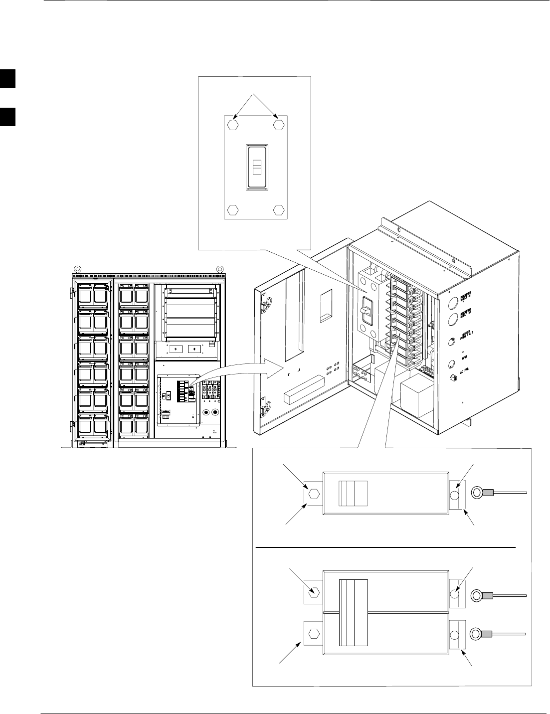
1Ensure the 400 Amp Main DC breaker and all other breakers in the RF Cabinet are OFF.
2Proceed to the DC Power Pre–test (BTS Frame) sequence (see Table 2-6) (for initial power–up as
required).
3Ensure the power cabinet is turned on (see Table 2-5). Verify that 27 volts is applied to the terminals
on the back of the RF cabinet.
4Engage the main DC circuit breaker on the RF cabinet (see Figure 2-5).
5On each RF cabinet:
SSet C–CCP shelf breakers to the ON position by pushing them in one at a time (labeled
C–CCP 1, 2, 3 – located on the power distribution panel).
SSet LPA breakers to the ON position by pushing them in one at a time (8 breakers, labeled 1A–1B
through 4C–4D – located on the power distribution panel).
SSet the two heat exchanger breakers to the ON position by pushing them in one at a time.
SSet the ETIB breaker to the ON position by pushing it in.
SSet the OPTION breaker to the ON position by pushing it in.
. . . continued on next page
2
Initial Power Up – continued
Jan 2002 2-9
SCt4812ET BTS Optimization/ATP — CDMA LMF
Table 2-7: RF Cabinet Power Up
Step Action
6Measure the voltage drop between the Power Cabinet meter test point and the 27 V buss bar inside the
RF Cabinet PDA while the RF Cabinet is transmitting.
NOTE
For a 3–sector carrier system, the voltage drop should be less than 0.2 V.
For a 12–sector carrier system, the voltage drop should be less than 0.3 V.
7Using a DC current probe, measure the current in each of the six (6) DC cables that are connected
between the RF and Power Cabinet. The DC current measured should be approximately the same. If
there is a wide variation between one cable and the others (>20 A), check the tightness of the
connections (torque settings) at each end of the cable.
RF CABINET
(Rear View)
27V
27V Ret
Figure 2-5: RF Cabinet Circuit Breaker Panel and 27Vdc Terminal Locations
MAIN BREAKER 5 RU RACK
SPACE
SC 4812ET BTS RF Cabinet
(Front View)
400
30
30
30
30
30
30
30
30
50
50
50
L
P
A
1B
1D
2B
2D
3B
3D
4B
4D
1A
1C
2A
2C
3A
3C
4A
4C
PS1
PS2
PS3
C
C
C
P
25
25
ETIB
OPTION
10
15
HEAT EXCHANGER
CAUTION
SHUT OFF BOTH BREAKERS
ONLY DURING HEAT EXCHANGER
MAINTENANCE OR REPAIR
LPA
BLOWERS
PUSH BUTTON
TO RESET
LPA BLOWERS
FW00307
I/O Plate + and – DC Feed
Terminals (Back Panel of RF
Cabinet)
2

Initial Power Up – continued
SCt4812ET BTS Optimization/ATP — CDMA LMF Jan 2002
2-10
Battery Charge Test
(Connected Batteries)
Table 2-8 lists the step–by–step instructions for testing the batteries.
Table 2-8: Battery Charge Test (Connected Batteries)
Step Action
1Close the battery compartment breakers for connected batteries ONLY. This process should be
completed quickly to avoid individual battery strings with excess charge current
NOTE
If the batteries are sufficiently discharged, the battery circuit breakers may not engage individually
due to the surge current. If this condition is observed, turn off the Meter Alarm Panel power switch,
and then engage all the connected battery circuit breakers, the Meter Alarm Panel power switch
should then be turned ON.
2Using the DC current probe, measure the current in each of the battery string connections to the buss
bars in each battery cabinet. The charge current may initially be high but should quickly reduce in a
few minutes if the batteries have a typical new battery charge level.
3The current in each string should be approximately equal (+ 5 A).
4The bargraph meters on the rectifier modules can be used as a rough estimate of the total battery
charge current. Each rectifier module has eight LEDs to represent the output current. Each illuminated
LED indicates that approximately 12.5% (1/8 or 8.75 A) of the rectifier’s maximum (70 A) current is
flowing.
EXAMPLE:
Question: A system fitted with three rectifier modules each have three bargraph LEDs illuminated.
What is the total output current into the batteries?
Answer: Each bargraph is approximately indicating 12.5% of 70 A, therefore, 3 X 8.75A equals
26.25A. As there are three rectifiers, the total charge current is equal to (3 X 26.25 A) 78.75 A.
This charge current calculation only applies at this part of the start up procedure when the RF Cabinet
is not powered on, and the power cabinet heat exchanger is turned off.
5Allow a few minutes to ensure that the battery charge current stabilizes before taking any further
action. Recheck the battery current in each string. If the batteries had a reasonable charge, the current
in each string should reduce to less than 5 A.
6Recheck the DC output voltage. It should remain the same as measured in step 4 of the Power Up
Test.
NOTE
If discharged batteries are installed, all bargraphs may be illuminated on the rectifiers during the
charge test. This indicates that the rectifiers are at full capacity and are rapidly charging the batteries.
It is recommended in this case that the batteries are allowed to charge and stabilize as in the above
step before commissioning the site. This could take several hours.
Battery Discharge Test
Perform the test procedure in Table 2-9 only when the battery current is
less than 5 A per string. Refer to Table 2-8 for the procedures to check
current levels.
2
Initial Power Up – continued
Jan 2002 2-11
SCt4812ET BTS Optimization/ATP — CDMA LMF
Table 2-9: Battery Discharge Test
Step Action
1Turn the battery test switch on the Meter Alarm Panel, ON (see Figure 2-3). The rectifier output
voltage and current should decrease by approximately 10% as the batteries assume the load. Alarms
for the Meter Alarm Panel may occur.
2Measure the individual battery string current using the DC current probe. The battery discharge
current in each string should be approximately the same (within± 5 A).
3Turn Battery Test Switch OFF.
Failure to turn OFF the Battery Test Switch before leaving
the site, will result in low battery capacity and reduce
battery life.
CAUTION
Heat Exchanger Power Up
Table 2-10: Heat Exchanger Power Up
Step Action
1Turn the Power Cabinet Heat Exchanger breakers ON (seeFigure 2-6 for breaker location).
2The Heat Exchanger will now go into a five (5) minute test sequence. Ensure that the internal and
external fans are operating. Place a hand on the internal and external Heat Exchanger grills to feel for
air draft.
2
Initial Power Up – continued
SCt4812ET BTS Optimization/ATP — CDMA LMF Jan 2002
2-12
Core
Heat Exchanger
Assembly
POWER CABINET
Front View
OUT=OFF
IN=ON
Blower Assembly
Circuit Breaker
FW00181
Side View
Mounting
Bracket
T–30 Screw
Top (Internal) Blower
Fan Module
Blower
Power
Cord
Blower
Power
Cord
Bottom (Ambient) Blower
Fan Module
T–30 Screw
Mounting
Bracket
Figure 2-6: Heat Exchanger Blower Assembly
2
Initial Power Up – continued
Jan 2002 2-13
SCt4812ET BTS Optimization/ATP — CDMA LMF
LED Status
Figure 2-7: Power Cabinet Circuit Breaker Assemblies
A B C
BREAKER SYSTEM BREAKER
SHOULD BE RESET
IF ILLUMINATED OR
AFTER RESET OF
3 MAIN BREAKERS
TO RESET MAIN BREAKERS, PRESS
AND HOLD IN GREEN BUTTON WHILE
PRESSING 160 AMP BREAKER BUTTON
UNTIL LATCHED RELEASE GREEN BUTTON
AFTER ALL 3 BREAKERS HAVE BEEN RESET
ON OFF
BREAKER SYSTEM
BREAKER
SYSTEM RESET
BUTTON
FW00144
POWER CABINET
Front View
AC Circuit
Breaker
DC Circuit
Breaker
160 160 160
25
25
Circuit Breaker Legend:
1. Main 150 Amp. . . . . . . . . . . . . . .
2. Rectifier Shelf #1 70 Amp. . . .
3. Rectifier Shelf #2 70 Amp. . . .
4. Battery Heater #1 15 Amp. . . .
5. Battery Heater #2 15 Amp. . . .
6. GFCI 15 Amp. . . . . . . . . . . . . . .
7. Spare 15 Amp. . . . . . . . . . . . . .
RECTIFIER
SHELF #1
RECTIFIER
SHELF #2
BATTERY
HEATER #1
GFCI
SPARE
BATTERY
HEATER #2
CAUTION
LIVE TERMINALS
2
3
4
5
6
1
7
ATTENTION
MAIN
2
Initial Power Up – continued
SCt4812ET BTS Optimization/ATP — CDMA LMF Jan 2002
2-14
15 Amp Breaker
5/16 NUT
LEFT TAB
SCREW
WIRE
RIGHT TAB
30 Thru 140 Amp Breaker
Figure 2-8: Power Cabinet AC Circuit Breakers
150 Amp Breaker
7/16 NUT
POWER CABINET
Front View
AC Circuit Breaker
FW00145
SCREW
WIRE
RIGHT
TABS
WIRE
5/16 NUT
LEFT TABS
2
Initial Power Up – continued
Jan 2002 2-15
SCt4812ET BTS Optimization/ATP — CDMA LMF
Figure 2-9: Power Cabinet DC Circuit Breakers
POWER CABINET
Front View
DC Circuit Breaker
FW00146
15 AMP
3x150 AMP
Flat Washer
Lock Washer 17 mm Nut
DC Power
Panel Door
Locks
9/32 Nut
2

Initial Power Up – continued
SCt4812ET BTS Optimization/ATP — CDMA LMF Jan 2002
2-16
Notes
2

Jan 2002 SCt4812ET BTS Optimization/ATP — CDMA LMF
Chapter 3: Optimization/Calibration
Table of Contents
Optimization/Calibration – Introduction
Introduction 3-1. . . . . . . . . . . . . . . . . . . . . . . . . . . . . . . . . . . . . . . . . . . . . .
Optimization Process 3-1. . . . . . . . . . . . . . . . . . . . . . . . . . . . . . . . . . . . . . .
Cell–site Types 3-2. . . . . . . . . . . . . . . . . . . . . . . . . . . . . . . . . . . . . . . . . . . .
Cell–site Data File 3-2. . . . . . . . . . . . . . . . . . . . . . . . . . . . . . . . . . . . . . . . .
BTS System Software Download 3-3. . . . . . . . . . . . . . . . . . . . . . . . . . . . .
Site Equipage Verification 3-3. . . . . . . . . . . . . . . . . . . . . . . . . . . . . . . . . . .
Isolate Span Lines/Connect LMF
Isolate BTS from T1/E1 Spans 3-4. . . . . . . . . . . . . . . . . . . . . . . . . . . . . . .
Configure Channel Service Unit 3-4. . . . . . . . . . . . . . . . . . . . . . . . . . . . . .
Alarm and Span Line Cable Pin/Signal Information 3-6. . . . . . . . . . . . . . .
T1/E1 Span Isolation 3-9. . . . . . . . . . . . . . . . . . . . . . . . . . . . . . . . . . . . . . .
Preparing the LMF
LMF Operating System Installation 3-10. . . . . . . . . . . . . . . . . . . . . . . . . . .
CDMA LMF Home Directory 3-11. . . . . . . . . . . . . . . . . . . . . . . . . . . . . . . .
Copy CBSC CDF Files to the LMF Computer 3-12. . . . . . . . . . . . . . . . . . .
Creating a Named HyperTerminal Connection for MMI Connection 3-13. .
Folder Structure Overview 3-16. . . . . . . . . . . . . . . . . . . . . . . . . . . . . . . . . . .
LMF to BTS Connection 3-17. . . . . . . . . . . . . . . . . . . . . . . . . . . . . . . . . . . .
Pinging the Processors 3-19. . . . . . . . . . . . . . . . . . . . . . . . . . . . . . . . . . . . . .
Log into and out ofthe BTSLMF PC 3-20. . . . . . . . . . . . . . . . . . . . . . . . . . .
Download Files to the LMF – Site Specific BTS Files 3-21. . . . . . . . . . . . .
Download Files to the LMF – Master–bts–cdma Files 3-22. . . . . . . . . . . . .
Create BTS Specific CDF File 3-24. . . . . . . . . . . . . . . . . . . . . . . . . . . . . . .
Update BTS Specific CDF File Device Load Version and Site Type 3-25. .
Update Antenna Mapping Files 3-26. . . . . . . . . . . . . . . . . . . . . . . . . . . . . . .
Using CDMA LMF
Basic LMF Operation 3-27. . . . . . . . . . . . . . . . . . . . . . . . . . . . . . . . . . . . . .
Basic LMF Operation 3-27. . . . . . . . . . . . . . . . . . . . . . . . . . . . . . . . . . . . . .
Logging into a BTS 3-28. . . . . . . . . . . . . . . . . . . . . . . . . . . . . . . . . . . . . . . .
Logging Out 3-31. . . . . . . . . . . . . . . . . . . . . . . . . . . . . . . . . . . . . . . . . . . . . .
Establishing an MMI Communication Session 3-33. . . . . . . . . . . . . . . . . . .
Download the BTS
Overview 3-34. . . . . . . . . . . . . . . . . . . . . . . . . . . . . . . . . . . . . . . . . . . . . . . .
Verify GLI ROM Code Loads 3-35. . . . . . . . . . . . . . . . . . . . . . . . . . . . . . . .
Download RAM Code and Data to MGLI and GLI 3-36. . . . . . . . . . . . . . .
. . . continued on next page
3

Table of Contents – continued
SCt4812ET BTS Optimization/ATP — CDMA LMF Jan 2002
Download RAM Code and Data to Non–GLI Devices 3-37. . . . . . . . . . . . .
Select CSM Clock Source 3-38. . . . . . . . . . . . . . . . . . . . . . . . . . . . . . . . . . .
Enable CSMs 3-38. . . . . . . . . . . . . . . . . . . . . . . . . . . . . . . . . . . . . . . . . . . . .
Enable MCCs 3-40. . . . . . . . . . . . . . . . . . . . . . . . . . . . . . . . . . . . . . . . . . . . .
CSM System Time – GPS & LFR/HSO Verification
Clock Synchronization Manager System Time 3-41. . . . . . . . . . . . . . . . . . .
LFR/HSO 3-41. . . . . . . . . . . . . . . . . . . . . . . . . . . . . . . . . . . . . . . . . . . . . . . .
CSM Frequency Verification 3-43. . . . . . . . . . . . . . . . . . . . . . . . . . . . . . . . .
Test Equipment Setup
(GPS & LFR/HSO Verification) 3-43. . . . . . . . . . . . . . . . . . . . . . . . . . . . . .
GPS Initialization/Verification 3-44. . . . . . . . . . . . . . . . . . . . . . . . . . . . . . . .
LORAN–C Initialization/Verification 3-49. . . . . . . . . . . . . . . . . . . . . . . . . .
Test Equipment Set–up
Connecting Test Equipment to the BTS 3-51. . . . . . . . . . . . . . . . . . . . . . . .
Supported Test Sets 3-51. . . . . . . . . . . . . . . . . . . . . . . . . . . . . . . . . . . . . . . .
Equipment Warm-up 3-55. . . . . . . . . . . . . . . . . . . . . . . . . . . . . . . . . . . . . . .
TX ATP Setup 3-67. . . . . . . . . . . . . . . . . . . . . . . . . . . . . . . . . . . . . . . . . . . .
Test Set Calibration
Background 3-69. . . . . . . . . . . . . . . . . . . . . . . . . . . . . . . . . . . . . . . . . . . . . .
Purpose 3-69. . . . . . . . . . . . . . . . . . . . . . . . . . . . . . . . . . . . . . . . . . . . . . . . .
GPIB Addresses 3-70. . . . . . . . . . . . . . . . . . . . . . . . . . . . . . . . . . . . . . . . . . .
Selecting Test Equipment 3-70. . . . . . . . . . . . . . . . . . . . . . . . . . . . . . . . . . .
Manually Selecting Test Equipment in a Serial Connection Tab 3-70. . . . .
Automatically Selecting Test Equipment in a Serial Connection Tab 3-72. .
Calibrating Test Equipment 3-73. . . . . . . . . . . . . . . . . . . . . . . . . . . . . . . . . .
Calibrating Cables 3-73. . . . . . . . . . . . . . . . . . . . . . . . . . . . . . . . . . . . . . . . .
Calibrating Cables with a CDMA Analyzer 3-74. . . . . . . . . . . . . . . . . . . . .
Calibrating TX Cables Using a Signal Generator and Spectrum Analyze 3-75
Calibrating RX Cables Using a Signal Generator and Spectrum Analyzer 3-76. .
Setting Cable Loss Values 3-77. . . . . . . . . . . . . . . . . . . . . . . . . . . . . . . . . . .
Setting Coupler Loss Value 3-78. . . . . . . . . . . . . . . . . . . . . . . . . . . . . . . . . .
Bay Level Offset Calibration
Introduction 3-79. . . . . . . . . . . . . . . . . . . . . . . . . . . . . . . . . . . . . . . . . . . . . .
RF Path Bay Level Offset Calibration 3-79. . . . . . . . . . . . . . . . . . . . . . . . . .
When to Calibrate BLOs 3-79. . . . . . . . . . . . . . . . . . . . . . . . . . . . . . . . . . . .
TX Path Calibration 3-80. . . . . . . . . . . . . . . . . . . . . . . . . . . . . . . . . . . . . . . .
BLO Calibration Data File 3-81. . . . . . . . . . . . . . . . . . . . . . . . . . . . . . . . . .
Test Equipment Setup: RF Path Calibration 3-83. . . . . . . . . . . . . . . . . . . . .
Transmit (TX) Path Calibration 3-84. . . . . . . . . . . . . . . . . . . . . . . . . . . . . . .
Download BLO Procedure 3-87. . . . . . . . . . . . . . . . . . . . . . . . . . . . . . . . . . .
Calibration Audit Introduction 3-88. . . . . . . . . . . . . . . . . . . . . . . . . . . . . . .
Transmit (TX) Path Audit 3-88. . . . . . . . . . . . . . . . . . . . . . . . . . . . . . . . . . .
TX Audit Test 3-89. . . . . . . . . . . . . . . . . . . . . . . . . . . . . . . . . . . . . . . . . . . .
All Cal/Audit Test 3-91. . . . . . . . . . . . . . . . . . . . . . . . . . . . . . . . . . . . . . . . .
Create CAL File 3-93. . . . . . . . . . . . . . . . . . . . . . . . . . . . . . . . . . . . . . . . . . .
. . . continued on next page
3

Table of Contents – continued
Jan 2002 SCt4812ET BTS Optimization/ATP — CDMA LMF
RFDS Setup and Calibration
RFDS Description 3-94. . . . . . . . . . . . . . . . . . . . . . . . . . . . . . . . . . . . . . . . .
RFDS Parameters 3-94. . . . . . . . . . . . . . . . . . . . . . . . . . . . . . . . . . . . . . . . . .
Checking and Setting RFDS Parameters 3-94. . . . . . . . . . . . . . . . . . . . . . . .
RFDS TSU NAM Programming 3-97. . . . . . . . . . . . . . . . . . . . . . . . . . . . . .
Explanation of Parameters Used When Programming the TSU NAM 3-97.
Valid NAM Ranges 3-98. . . . . . . . . . . . . . . . . . . . . . . . . . . . . . . . . . . . . . . .
Set Antenna Map Data 3-99. . . . . . . . . . . . . . . . . . . . . . . . . . . . . . . . . . . . . .
Set RFDS Configuration Data 3-100. . . . . . . . . . . . . . . . . . . . . . . . . . . . . . . .
RFDS Calibration 3-101. . . . . . . . . . . . . . . . . . . . . . . . . . . . . . . . . . . . . . . . .
RFDS Calibration Procedure 3-101. . . . . . . . . . . . . . . . . . . . . . . . . . . . . . . . .
Program TSU NAM 3-103. . . . . . . . . . . . . . . . . . . . . . . . . . . . . . . . . . . . . . . .
Alarms Testing
Alarm Verification 3-104. . . . . . . . . . . . . . . . . . . . . . . . . . . . . . . . . . . . . . . . .
Alarm Reporting Display 3-104. . . . . . . . . . . . . . . . . . . . . . . . . . . . . . . . . . . .
Heat Exchanger Alarm Test 3-105. . . . . . . . . . . . . . . . . . . . . . . . . . . . . . . . . .
Door Alarm 3-105. . . . . . . . . . . . . . . . . . . . . . . . . . . . . . . . . . . . . . . . . . . . . .
AC Fail Alarm 3-105. . . . . . . . . . . . . . . . . . . . . . . . . . . . . . . . . . . . . . . . . . . .
Minor Alarm 3-106. . . . . . . . . . . . . . . . . . . . . . . . . . . . . . . . . . . . . . . . . . . . .
Rectifier Alarms 3-106. . . . . . . . . . . . . . . . . . . . . . . . . . . . . . . . . . . . . . . . . . .
Single Rectifier Failure (Three Rectifier System) 3-106. . . . . . . . . . . . . . . . .
Multiple Rectifier Failure 3-107. . . . . . . . . . . . . . . . . . . . . . . . . . . . . . . . . . .
Single Rectifier Failure
(Six Rectifier System) 3-107. . . . . . . . . . . . . . . . . . . . . . . . . . . . . . . . . . . . . .
Multiple Rectifier Failure (Six Rectifier System) 3-108. . . . . . . . . . . . . . . . .
Battery Over Temperature Alarm (Optional) 3-108. . . . . . . . . . . . . . . . . . . . .
Rectifier Over Temperature Alarm 3-110. . . . . . . . . . . . . . . . . . . . . . . . . . . .
Before Leaving the site 3-111. . . . . . . . . . . . . . . . . . . . . . . . . . . . . . . . . . . . .
3

Table of Contents – continued
SCt4812ET BTS Optimization/ATP — CDMA LMF Jan 2002
Notes
3
Optimization/Calibration – Introduction
Jan 2002 3-1
SCt4812ET BTS Optimization/ATP — CDMA LMF
Introduction
This chapter provides procedures for downloading system operating
software, set up of the supported test equipment, CSM reference
verification/optimization, and transmit/receive path verification.
Before using the LMF, use an editor to view the
”CAVEATS” section in the ”readme.txt” file in the c:\wlmf
folder for any applicable information.
IMPORTANT
*
Optimization Process
After a BTS is physically installed and the preliminary operations
(power up) have been completed, the CDMA LMF is used to calibrate
and optimize the BTS. The basic optimization process can be
accomplished as follows:
SDownload MGLI2–1 with code and data and then enable MGLI2–1.
SUse the status function and verify that all of the installed devices of
the following types respond with status information: CSM, BBX,
GLI2, and MCC (and TSU if RFDS is installed). If a device is
installed and powered up but is not responding and is colored gray in
the BTS display, the device is not listed in the CDF file. The CDF file
will have to be corrected before the device can be accessed by CDMA
LMF.
SDownload code and data to all devices of the following types:
–CSM
–BBX (may be BBX2 or BBX–1X)
–GLI2 (other than GLI2–1)
–MCC (may be MCC–8E, MCC24, or MCC–1X)
SDownload the RFDS TSIC (if installed).
SVerify the operation of the GPS and HSO or LFR signals.
SEnable the following devices (in the order listed):
–Secondary CSM (slot 2)
–Primary CSM (slot 1)
–All MCCs
SConnect the required test equipment for a full optimization.
SSelect the test equipment.
SCalibrate the TX and RX test cables if they have not previously been
calibrated using the CDMA LMF that is going to be used for the
optimization/calibration. The cable calibration values can also be
entered manually.
3

Optimization/Calibration – Introduction – continued
SCt4812ET BTS Optimization/ATP — CDMA LMF Jan 2002
3-2
SSelect all of the BBXs and all of the MCCs and use the full
optimization function. The full optimization function performs TX
calibration, BLO download, TX audit, all TX tests, and all RX tests
for all selected devices.
SIf the TX calibration fails, repeat the full optimization for any failed
paths.
SIf the TX calibration fails again, correct the problem that caused the
failure and repeat the full optimization for the failed path.
SIf the TX calibration and audit portion of the full optimization passes
for a path but some of the TX or RX tests fail, correct the problem that
caused the failure and run the individual tests as required until all TX
and RX tests have passed for all paths.
Cell–site Types
Sites are configured as Omni/Omni or Sector/Sector (TX/RX). Each type
has unique characteristics and must be optimized accordingly.
Cell–site Data File
BTSs may contain a mixture of BBX2 cards and BBX–1X cards. When
this is the case, the redundant BBX card must be a BBX–1X card.
The CDF includes the following information:
SDownload instructions and protocol
SSite specific equipage information
SC–CCP shelf allocation plan
–BBX equipage (based on cell–site type) including redundancy
–CSM equipage including redundancy
–MCC (MCC24E, MCC8E or MCC–1X) channel element allocation
plan. This plan indicates how the C–CCP shelf is configured, and
how the paging, synchronization, traffic, and access channel
elements (and associated gain values) are assigned among the (up to
12) MCCs in the shelf.
SCSM equipage including redundancy
SEffective Rated Power (ERP) table for all TX channels to antennas
respectively. Motorola System Engineering specifies the ERP of a
transmit antenna based on site geography, antenna placement, and
government regulations. Working from this ERP requirement, the
antenna gain, (dependent on the units of measurement specified) and
antenna feed line loss can be combined to determine the required
power at the top of the BTS frame. The corresponding BBX output
level required to achieve that power level on any channel/sector can
also be determined.
Refer to the CDMA LMF Operator’s Guide,, for additional
information on the layout of the LMF directory structure
(including CDF file locations and formats).
NOTE
3
Optimization/Calibration – Introduction – continued
Jan 2002 3-3
SCt4812ET BTS Optimization/ATP — CDMA LMF
BTS System Software
Download
BTS system software must be successfully downloaded to the BTS
processor boards before optimization can be performed. BTS operating
code is loaded from the LMF computer terminal.
Before using the LMF for optimization/ATP, the correct
bts–#.cdf and cbsc–#.cdf files for the BTS must be
obtained from the CBSC and put in a bts–# folder in the
LMF. Failure to use the correct CDF files can cause wrong
results. Failure to use the correct CDF files to log into a
live (traffic carrying) site can shut down the site.
IMPORTANT
*
The CDF is normally obtained from the CBSC on a DOS formatted
diskette, or through a file transfer protocol (ftp) if the LMF computer has
ftp capability. Refer to the CDMA LMF Operator’s Guide, or the LMF
Help screen, for more information.
Site Equipage Verification
If you have not already done so, use an editor to view the CDF, and
review the site documentation. Verify the site engineering equipage data
in the CDF to the actual site hardware.
Always wear a conductive, high impedance wrist strap
while handling any circuit card/module to prevent damage
by ESD. Extreme care should be taken during the removal
and installation of any card/module. After removal, the
card/module should be placed on a conductive surface or
back into the anti–static bag in which it was shipped.
CAUTION
3

Isolate Span Lines/Connect LMF
SCt4812ET BTS Optimization/ATP — CDMA LMF Jan 2002
3-4
Isolate BTS from T1/E1 Spans
–At active sites, the OMC/CBSC must disable the
BTS and place it out of service (OOS). DO NOT
remove the span surge protectors until the
OMC/CBSC has disabled the BTS.
IMPORTANT
*
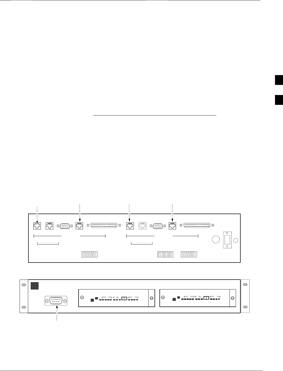
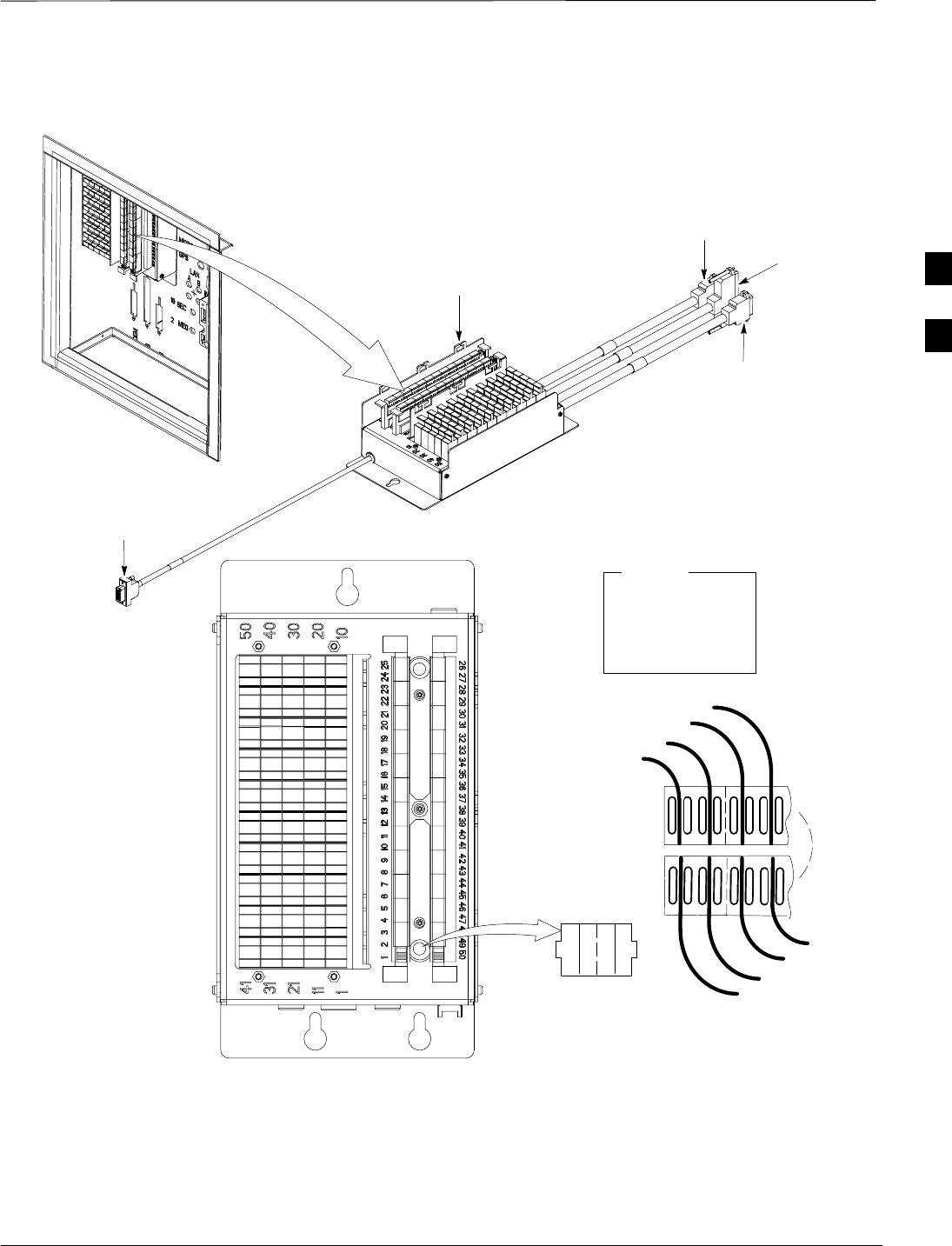
Each frame is equipped with one 50–pair punch block for spans,
customer alarms, remote GPS, and power cabinet alarms. See Figure 3-2
and refer to Table 3-1 for the physical location and pin call–out
information. To disable the span, pull the surge protectors for the
respective span.
Before connecting the LMF to the frame LAN, the OMC/CBSC must
disable the BTS and place it OOS to allow the LMF to control the
CDMA BTS. This prevents the CBSC from inadvertently sending
control information to the CDMA BTS during LMF based tests.
Configure Channel Service
Unit
The M–PATH 537 Channel Service Unit (CSU) provides in–band
SNMP–managed digital service access to T1 and fractional T1 lines.
M–PATH units plug into the Kentrox 2–slot frame (see Figure 3-1).
Remote M–PATH management is available via SNMP over an in–band
data link on the T1 line (using a facility data link or 8–64 kbps of a DS0
channel). The unit at the near end of the management path can be an
SNMP manager or another M–PATH CSU.
Each 19 inch rack can support two CSU M–PATH 537 modules. Each
M–PATH 537 module supports one and only one span connection.
Programming of the M–PATH is accomplished through the DCE 9–pin
connector on the front panel of the CSU shelf. Manuals and a Microsoft
Windows programming disk is supplied with each unit.
3
Isolate Span Lines/Connect LMF – continued
Jan 2002 3-5
SCt4812ET BTS Optimization/ATP — CDMA LMF
Setting the Control Port
Whichever control port is chosen, it must first be set up so the control
port switches match the communication parameters being used by the
control device. If using the rear–panel DTE control port, set the
shelf–address switch SA5 to “up” (leave the switch down for the
rear–panel DCE control port).
For more information, refer to the vendor user manual (part number
1174139) and installation manual (part number 1174462) provided with
each CSU.
Plug one of the cables listed below into the Control Port connectors:
Part Number Description of Cable
01–95006–022 (six feet) DB–9S to DB–9P
01–95010–022 (ten feet)
The control port cables can be used to connect the shelf to:
SA PC using the AT 9–pin interface
SA modem using the 9–pin connector
SOther shelves in a daisy chain
Figure 3-1: Back and Front View of the CSU
REF. FW00212
Front View
SLOT 1 SLOT 2
DCE Connector
(Craft Port)
SLOT 1SLOT 2 T1 TERMINAL T1 TERMINAL
CONTROL
PORT GROUP
ADDRESS SHELF
ADDRESS
T1 DDS T1 DDS
DTE DCEDATA PORT DATA PORT
Back View
NETWORK NETWORK
To/From
Network To/From
GLI
To/From
Network To/From
GLI
3

Isolate Span Lines/Connect LMF – continued
SCt4812ET BTS Optimization/ATP — CDMA LMF Jan 2002
3-6
SC4812ET Span Line Labeling for Span B and Span C is
swapped
–On the SC4812ET’s, the span cabel internal to the base
station that connects the 50 pin header on the I/O plate to
the CSU has Span B and Span C (RJ–45) connectors
mis–labeled.
–CFE will punch down the span on the 50 pair bunchblock
as per Motorola documentation and punchdown chart.
When conecting the span input to the CSU re–label
“Span B” cable to”Span C” cable to “Span B”. Connect
to CSU as per documentation
–Note: The labeling issue on the cable from the I/O plate
to the CSU Part Number 3086601H01 Rev C shall be
corrected on revision “D” to address this issue. The cut
over date to Rev. D will be approximately January 30,
2001.
CAUTION
Alarm and Span Line Cable
Pin/Signal Information
See Figure 3-2 and refer toTable 3-1for the physical location and pin
call–out information for the 50–pin punch block.
3
Isolate Span Lines/Connect LMF – continued
Jan 2002 3-7
SCt4812ET BTS Optimization/ATP — CDMA LMF
Figure 3-2: 50 Pair Punch Block
TOP VIEW OF PUNCH BLOCK
STRAIN RELIEVE INCOMING
CABLE TO BRACKET WITH
TIE WRAPS
2T
1T 1R 2T 2R
12
1R
2R
LEGEND
1T = PAIR 1 – TIP
1R = PAIR 1 –RING
” ”
” ”
” ”
RF Cabinet I/O Area
50R
50T
49R
49T
1T
FW00162
TO LAN
CONNECTOR
TO ALARMS
CONNECTOR
TO MODEM
CONNECTOR
TO RGD/RGPS
CONNECTOR
3
Isolate Span Lines/Connect LMF – continued
SCt4812ET BTS Optimization/ATP — CDMA LMF Jan 2002
3-8
Alarm and Span Line Cable
Pin/Signal Information
Table 3-1 lists the complete pin/signal identification for the 50–pin
punch block.
Table 3-1: Pin–Out for 50–Pair Punchblock
Punchblock
Cable
Connector Function Signal Name Punch Pin Ext. Cable Wire
Color
Power Cab Control – NC 1T Blue
Power Cab Control – NO 1R Blk/Blue
Power Cab Control–Com 2T Yellow
Reserved 2R N/C
Rectifier Fail 3T Blk/Yellow
AC Fail 3R Green
Power Cabinet Power Cab Exchanger Fail 4T Blk/Grn
Power Cab Door Alarm 4R White
Power Cab Major Alarm 5T Blk/White
Battery Over Temp 5R Red
Power Cab Minor Alarm 6T Blk/Red
Reticifier Over Temp 6R Brown
Power Cab Alarm Rtn 7T Blk/Brn
ALARM LFR_HSO_GND 7R
HSO/LFR EXT_1PPS_POS 8T
Extension EXT_1PPS_NEG 8R
CAL_+ 9T
CAB_–9R
LFR Antenna LORAN_+ 10T
LORAN_–10R
Pilot Beacon Alarm – Minor 11T
Pilot Beacon Alarm – Rtn 11R
Pilot Beacon Alarm – Major 12T
Pilot Beacon Pilot Beacon Control–NO 12R
Pilot Beacon Control – COM 13T
Pilot Beacon Control – NC 13R
. . . continued on next page
3
Isolate Span Lines/Connect LMF – continued
Jan 2002 3-9
SCt4812ET BTS Optimization/ATP — CDMA LMF
Table 3-1: Pin–Out for 50–Pair Punchblock
Punchblock
Cable
Connector
Ext. Cable Wire
Color
Punch PinSignal Name
Function
Customer Outputs 1 – NO 14T
Customer Outputs 1 – COM 14R
Customer Outputs 1 – NO 14T
Customer Outputs 1 – COM 14R
Customer Outputs 1 – NC 15T
Customer Outputs 2 – NO 15R
Customer Outputs 2 – COM 16T
ALARM Customer Outputs Customer Outputs 2 – NC 16R
Customer Outputs 3 – NO 17T
Customer Outputs 3 – COM 17R
Customer Outputs 3 – NC 18T
Customer Outputs 4 – NO 18R
Customer Outputs 4–COM 19T
Customer Outputs 4 – NC 19R
. . . continued on next page
3
Isolate Span Lines/Connect LMF – continued
SCt4812ET BTS Optimization/ATP — CDMA LMF Jan 2002
3-10
Table 3-1: Pin–Out for 50–Pair Punchblock
Punchblock
Cable
Connector
Ext. Cable Wire
Color
Punch PinSignal Name
Function
Customer Inputs 1 20T
Cust_Rtn_A_1 20R
Customer Inputs 2 21T
Cust_Rtn_A_2 21R
Customer Inputs 3 22T
Cust_Rtn_A_3 22R
Customer Inputs 4 23T
Cust_Rtn_A_4 23R
Customer Inputs 5 24T
Cust_Rtn_A_5 24R
ALARM Customer Inputs Customer Inputs 6 25T
Cust_Rtn_A_6 25R
Customer Inputs 7 26T
Cust_Rtn_A_7 26R
Customer Inputs 8 27T
Cust_Rtn_A_8 27R
Customer Inputs 9 28T
Cust_Rtn_A_9 28R
Customer Inputs 10 29T
Cust_Rtn_A_10 29R
. . . continued on next page
3
Isolate Span Lines/Connect LMF – continued
Jan 2002 3-11
SCt4812ET BTS Optimization/ATP — CDMA LMF
Table 3-1: Pin–Out for 50–Pair Punchblock
Punchblock
Cable
Connector
Ext. Cable Wire
Color
Punch PinSignal Name
Function
RCV_TIP_A 30T
RCV_RING_A 30R
Span 1 XMIT_TIP_A 31T
XMIT_RING_A 31R
RCV_TIP_B 32T
RCV_RING_B 32R
Span 2 XMIT_TIP_B 33T
XMIT_RING_B 33R
RCV_TIP_C (Note) 34T
RCV_RING_C (Note) 34R
Span 3 XMIT_TIP_C (Note) 35T
XMIT_RING_C(Note) 35R
RCV_TIP_D (Note) 36T
SPAN I/O RCV_RING_D (Note) 36R
Span 4 XMIT_TIP_D (Note) 37T
XMIT_RING_D(Note) 37R
RCV_TIP_E (Note) 38T
RCV_RING_E (Note) 38R
Span 5 XMIT_TIP_E (Note) 39T
XMIT_RING_E(Note) 39R
RCV_TIP_F (Note) 40T
RCV_RING_F (Note) 40R
Span 6 XMIT_TIP_F (Note) 41T
XMIT_RING_F(Note) 41R
NOTE
Span 3 through 6 are spares for expansion purposes
. . . continued on next page
3

Isolate Span Lines/Connect LMF – continued
SCt4812ET BTS Optimization/ATP — CDMA LMF Jan 2002
3-12
Table 3-1: Pin–Out for 50–Pair Punchblock
Punchblock
Cable
Connector
Ext. Cable Wire
Color
Punch PinSignal Name
Function
GPS_Power_A 42T Yellow
For frame GPS_Power_A_Return 42R Yellow/Black
without RGD GPS_Power_B 43T Blue
Expansion
Punchblock GPS_Power_B_Return 43R Blue/Black
Single Frame GPS_TXD+ 44T White
RGD/RGPS BTS;RGPS Head GPS_TXD–44R White/Black
Connection GPS_RXD+ 45T Green
OR
Multiple Frame GPS_RXD–45R Green/Black
Multiple Frame
BTS; RGD Signal Ground (TDR+) 46T Red
Connection at Signal Ground (TDR–) 46R Red/Black
RGPS Secondary
Frame GPS_1PPS+ 47T Brown
GPS_1PPS–47R Brown/Black
GPS_Power_A 42T Yellow
GPS_Power_A_Return 42R Yellow/Black
GPS_Power_B 43T Blue
For frame with GPS_Power_B_Return 43R Blue/Black
RGD Expansion
Punchblock GPS_TXD+ 44T White
OR GPS_TXD–44R White/Black
RGD/RGPS Multiple Frame
BTS; RGPS Head GPS_RXD+ 45T Green
BTS; RGPS Head
Connection at GPS_RXD–45R Green/Black
RGPS Primary
Frame Signal Ground (TDR+) 46T Red
Master Frame (TDR–) 46R Red/Black
GPS_1PPS+ 47T Brown
GPS_1PPS–47R Brown/Black
Reserved 48T
MODEM Reserved 48R
RGD/RGPS Chassis Ground 49T N/A
None No Connection 49R None
Reserved 50T None
ALARM Reserved 50R None
3

Isolate Span Lines/Connect LMF – continued
Jan 2002 3-13
SCt4812ET BTS Optimization/ATP — CDMA LMF
T1/E1 Span Isolation
Table 3-2 describes the action required for span isolation.
Table 3-2: T1/E1 Span Isolation
Step Action
1The OMC/CBSC must disable the BTS and place it OOS.
The Span Lines can be disabled by removing the surge protectors on the 50–pin punch block. Using
Table 3-1 locate the span or spans which need to be disabled and remove the respective surge
protector.
NOTE
If a third party is used for span connectivity, the third party must be informed before disabling the span
line.
3

Preparing the LMF
SCt4812ET BTS Optimization/ATP — CDMA LMF Jan 2002
3-14
Software and files for installation and updating of the LMF are provided
on CD ROM disks. The following installation items must be available:
SLMF Program on CD ROM
SLMF Binaries on CD ROM
SCDF for each supported BTS (on diskette or available from the
CBSC)
SCBSC File for each supported BTS (on diskette or available from the
CBSC)
The following section provides information and instructions for
installing and updating the LMF software and files.
LMF Operating System Installation
Follow the procedure in Table 3-3 to install the LMF operating system.
Table 3-3: LMF Operating System Installation
Step Action
1Insert the LMF Program CD ROM into the LMF CD ROM drive.
–If the Setup screen is displayed, go to step 5.
–If the Setup screen is not displayed, proceed to step 2.
2Click on the Start button.
3 Select Run.
4In the Open box, enter d:\autorun and click on the OK button.
NOTE
If applicable, replace the letter d with the correct CD ROM drive letter.
. . . continued on next page
3

Preparing the LMF – continued
Jan 2002 3-15
SCt4812ET BTS Optimization/ATP — CDMA LMF
Table 3-3: LMF Operating System Installation
Step Action
5Follow the instructions displayed on the Setup screen.
* IMPORTANT
First Time Installations:
–Install U/WIN (First)
–Install Java Runtime Environment (Second)
–Install LMF Software (Third)
–Install BTS Binaries (Fourth)
–Install/Create BTS Folders (Fifth)
Any time you install U/WIN, you must install the LMF software because the installation of the LMF
modifies some of the files that are installed during the U/Win installation. Installing U/Win
over–writes these modifications.
NOTE
There are multiple binary image packages for installation on the CD–ROM. When prompted, choose
the load that corresponds to the switch release that you currently have installed. Perform the Device
Images install after the WinLMF installation.
If applicable, a separate CD ROM of BTS Binaries may be available for binary updates.
CDMA LMF Home Directory
The CDMA LMF installation program creates the default home directory
c:\wlmf, and installs the application files and subdirectories (folders)
in it. Because this can be changed at installation, the CDMA LMF home
directory will be referred to with the generic convention of:
<x>:\<lmf home directory>
Where:
<x> = the LMF computer drive letter where the CDMA LMF home
directory is located.
<lmf home directory> = the directory path or name where the CDMA
LMF is installed
The CDMA LMF installation program creates the default
home directory c:\wlmf when the CDMA LMF is
installed.There are differences between Windows NT and
Windows 98 in the menus and screens for creating a
HyperTerminal connection. In the following procedure,
items applicable to:
NOTE
3
Preparing the LMF – continued
SCt4812ET BTS Optimization/ATP — CDMA LMF Jan 2002
3-16
Copy CBSC CDF Files to the
LMF Computer
Before logging on to a BTS with the LMF to execute optimization/ATP
procedures, the correct bts-#.cdf and cbsc–#.cdf files must be obtained
from the CBSC and put in a bts-# folder in the LMF computer. This
requires creating versions of the CBSC CDF files on a DOS–formatted
floppy diskette and using the diskette to install the CDF files on the
LMF computer.
*When copying CDF files, comply with the following to
prevent BTS login problems with the LMF.
– The numbers used in the bts–#.cdf and cbsc–#.cdf
filenames must correspond to the locally assigned numbers
for each BTS and its controlling CBSC.
– The generic cbsc–1.cdf file supplied with the LMF will
work with locally numbered BTS CDF files. Using this file
will not provide a valid optimization unless the generic file
is edited to replace default parameters (e.g., channel
numbers) with the operational parameters used locally.
IMPORTANT
The procedure in Table 3-4 lists the steps required to transfer the CDF
files from the CBSC to the LMF computer. For any further information,
refer to the CDMA LMF Operator’s Guide (Motorola part number
68P64114A21) or the LMF Help screen..
Table 3-4: Copying CBSC CDF Files to the LMF
Step Action
1Login to the CBSC workstation.
2Insert a DOS–formatted floppy diskette in the workstation drive.
3 Type eject –q and press <Enter>.
4 Type mount and press <Enter>.
NOTE
SLook for the “floppy/no_name” message on the last line displayed.
SIf the eject command was previously entered, floppy/no_name will be appended with a number. Use
the explicit floppy/no_name reference displayed when performing step 7.
5Change to the directory, where the files to be copied reside, by typing cd <directoryname>
(e.g., cd bts–248) and pressing <Enter>.
6 Type ls and press the Enter key to display the list of files in the directory.
. . . continued on next page
3

Preparing the LMF – continued
Jan 2002 3-17
SCt4812ET BTS Optimization/ATP — CDMA LMF
Table 3-4: Copying CBSC CDF Files to the LMF
Step Action
7 With Solaris versions of Unix, create DOS–formatted versions of the bts–#.cdf and cbsc–#.cdf files
on the diskette by entering the following command:
unix2dos <source filename> /floppy/no_name/<target filename>
(e.g., unix2dos bts–248.cdf /floppy/no_name/bts–248.cdf).
NOTE
SOther versions of Unix do not support the unix2dos and dos2unix commands. In these cases, use the
Unix cp (copy) command. The copied files will be difficult to read with a DOS or Windows text
editor because Unix files do not contain line feed characters. Editing copied CDF files on the LMF
computer is, therefore, not recommended.
SUsing cp, multiple files can be copied in one operation by separating each filename to be copied
with a space and ensuring the destination directory (floppy/no_name) is listed at the end of the
command string following a space (e.g., cp bts–248.cdf cbsc–6.cdf /floppy/na_name)
8Repeat steps 5 through 7 for each bts–# that must be supported by the LMF.
9When all required files have been copied to the diskette, type eject and press <Enter>.
10 Remove the diskette from the CBSC drive.
11 If it is not running, start the Windows operating system on the LMF computer.
12 Insert the diskette containing the bts–#.cdf and cbsc–#.cdf files into the LMF computer.
13 Using Windows Explorer (or equivalent program), create a corresponding bts–# folder in the <lmf
home directory> directory for each bts–#.cdf/cbsc–#.cdf file pair copied from the CBSC.
14 Use Windows Explorer (or equivalent program) to transfer the cbsc–#.cdf and bts–#.cdf files from the
diskette to the corresponding <lmf home directory>\cdma\bts–# folders created in step 13.
Creating a Named
HyperTerminal Connection for
MMI Connection
Confirming or changing the configuration data of certain BTS FRUs
requires establishing an MMI communication session between the LMF
and the FRU. Using features of the Windows operating system, the
connection properties for an MMI session can be saved on the LMF
computer as a named Windows HyperTerminal connection. This
eliminates the need for setting up connection parameters each time an
MMI session is required to support optimization.
Once the named connection is saved, a shortcut for it can be created on
the Windows desktop. Double clicking the shortcut icon will start the
connection without the need to negotiate multiple menu levels.
Follow the procedures in Table 3-5 to establish a named HyperTerminal
connection and create a Windows desktop shortcut for it.
3

Preparing the LMF – continued
SCt4812ET BTS Optimization/ATP — CDMA LMF Jan 2002
3-18
There are differences between Windows NT and Windows
98 in the menus and screens for creating a HyperTerminal
connection. In the following procedure, items applicable
to:
– Windows NT will be identified with Win NT
– Windows 98 will be identified with Win 98
NOTE
Table 3-5: Creating a Named Hyperlink Connection for MMI Connection
Step Action
1From the Windows Start menu, select:
Programs>Accessories
2Perform one of the following:
SFor Win NT, select Hyperterminal and then click on HyperTerminal or
SFor Win 98, select Communications, double click the Hyperterminal folder, and then double click
on the Hyperterm.exe icon in the window that opens.
NOTE
SIf a Location Information Window appears, enter the required information, then click Close.
(This is required the first time, even if a modem is not to be used.)
SIf a You need to install a modem..... message appears, click NO.
3When the Connection Description box opens:
–Type a name for the connection being defined (e.g., MMI Session) in the Name: window.
–Highlight any icon preferred for the named connection in the Icon: chooser window, and
–Click OK.
4
NOTE
For LMF configurations where COM1 is used by another interface such as test equipment and a
physical port is available for COM2, select COM2 to prevent conflicts.
From the Connect using: pick list in the Connect To box displayed, select the RS–232 port to be used
for the connection (e.g., COM1 or COM2 – Win NT – or Direct to Com 1 or Direct to Com 2 – Win
98), and click OK.
5In the Port Settings tab of the COM# Properties window displayed, configure the RS–232 port
settings as follows:
SBits per second: 9600
SData bits: 8
SParity: None
SStop bits: 1
SFlow control: None
. . . continued on next page
3

Preparing the LMF – continued
Jan 2002 3-19
SCt4812ET BTS Optimization/ATP — CDMA LMF
Table 3-5: Creating a Named Hyperlink Connection for MMI Connection
Step Action
6 Click OK.
7Save the defined connection by selecting:
File>Save
8Close the HyperTerminal window by selecting:
File>Exit
9 Click Yes to disconnect when prompted.
10 Perform one of the following:
SIf the Hyperterminal folder window is still open (Win 98) proceed to step 12 or
SFrom the Windows Start menu, select Programs > Accessories
11 Perform one of the following:
SFor Win NT, select Hyperterminal and release any pressed mouse buttons.
SFor Win 98, select Communications and double click the Hyperterminal folder.
12 Highlight the newly created connection icon by moving the cursor over it (Win NT) or clicking on it
(Win 98).
13 Right click and drag the highlighted connection icon to the Windows desktop and release the right
mouse button.
14 From the popup menu displayed, select Create Shortcut(s) Here.
15 If desired, reposition the shortcut icon for the new connection by dragging it to another location on the
Windows desktop.
3

Preparing the LMF – continued
SCt4812ET BTS Optimization/ATP — CDMA LMF Jan 2002
3-20
Folder Structure Overview
The CDMA LMF installation program creates the default home directory
c:\wlmf, and installs the application files and subdirectories (folders) in
it. Because this can be changed at installation, the CDMA LMF home
directory will be referred to with the generic convention of:
<x>:\<lmf home directory>
Where:
<x> = the LMF computer drive letter where the CDMA LMF home
directory is located
<lmf home directory> = the directory path or name where the CDMA
LMF is installed.
Figure 3-3: LMF Folder Structure
version folder (A separate folder is
required for each different version; for
example, a folder name 2.8.1.1.1.5)
loads folder
<x>:\ (drive letter)
<lmf home directory> folder
cdma folder
code folder
data folder
BTS–nnn folders (A separate folder is
required for each BTS where bts–nnn is the
unique BTS number; for example, bts–163)
3

Preparing the LMF – continued
Jan 2002 3-21
SCt4812ET BTS Optimization/ATP — CDMA LMF
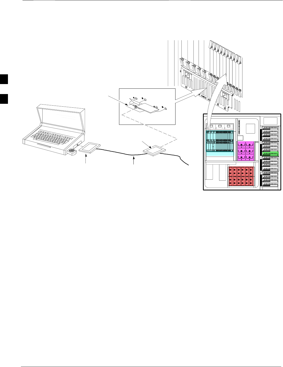
LMF to BTS Connection
The LMF is connected to the LAN A or B connector located on the left
side of the frame’s lower air intake grill, behind the LAN Cable Access
door (see Figure 3-4).
Table 3-6: LMF to BTS Connection
Step Action
1To gain access to the connectors, open the LAN Cable Access door, then pull apart the Velcro tape
covering the BNC “T” connector and slide out the computer service tray, if desired (see Figure 3-4).
2Connect the LMF to the LAN A BNC connector via PCMCIA Ethernet Adapter with an unshielded
twisted–pair (UTP) Adapter and 10BaseT/10Base2 converter (powered by an external AC/DC
transformer). If there is no login response, connect the LMF to the LAN B BNC connector. If there is
still no login response, see Table 6-1, Login Failure Troubleshooting Procedure.
NOTE
–Xircom Model PE3–10B2 or equivalent can also be used to interface the LMF Ethernet
connection to the frame connected to the PC parallel port, powered by an external AC/DC
transformer. In this case, the BNC cable must not exceed 91 cm (3 ft) in length.
* IMPORTANT
The LAN shield is isolated from chassis ground. The LAN shield (exposed portion of BNC connector)
must not touch the chassis during optimization.
3
Preparing the LMF – continued
SCt4812ET BTS Optimization/ATP — CDMA LMF Jan 2002
3-22
RFDS
EBA
ETIB
LMF BNC “T” CONNECTIONS
ON LEFT SIDE OF FRAME
(ETHERNET “A” SHOWN;
ETHERNET “B” COVERED
WITH VELCRO TAPE)
LMF COMPUTER
TERMINAL WITH
MOUSE PCMCIA ETHERNET
ADPATER & ETHERNET
UTP ADAPTER
UNIVERSAL TWISTED
PAIR (UTP) CABLE (RJ11
CONNECTORS)
10BASET/10BASE2
CONVERTER CONNECTS
DIRECTLY TO BNC T
115 VAC POWER
CONNECTION
FW00168
SC4812ET RF CABINET
NOTE:
Open LAN CABLE ACCESS
door. Pull apart Velcro tape and
gain access to the LAN A or LAN
B LMF BNC connector.
Figure 3-4: LMF Connection Detail
3
Preparing the LMF – continued
Jan 2002 3-23
SCt4812ET BTS Optimization/ATP — CDMA LMF
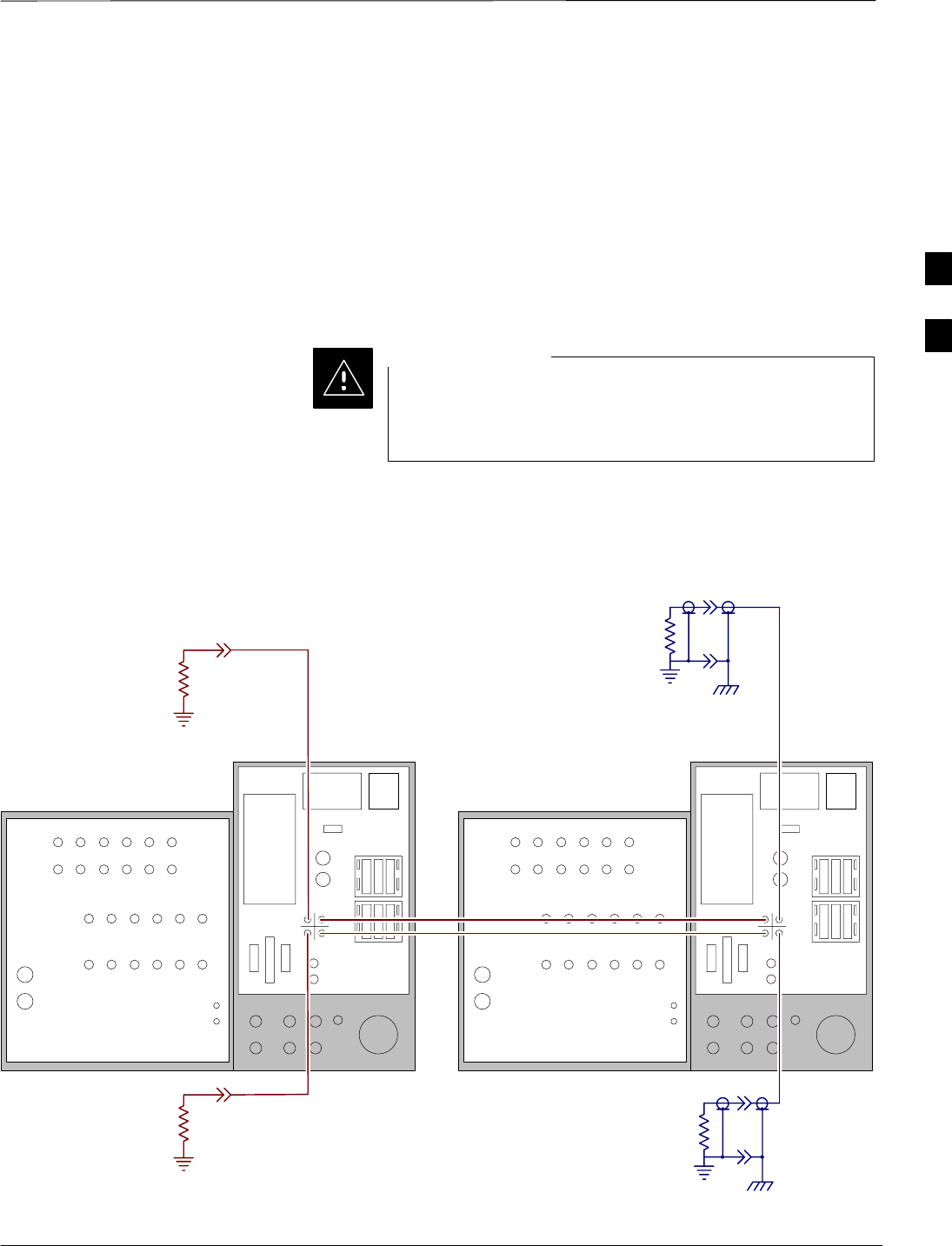
Pinging the Processors
For proper operation, the integrity of the Ethernet LAN A and B links
must be be verified. Figure 3-5 represents a typical BTS Ethernet
configuration. The drawing depicts one (of two identical) links, A and B.
Ping is a program that sends request packets to the LAN network
modules to get a response from the specified “target” module.
Follow the steps in Table 3-7 to ping each processor (on both LAN A
and LAN B) and verify LAN redundancy is working properly.
Always wear a conductive, high impedance wrist strap
while handling any circuit card/module to prevent damage
by ESD.
CAUTION
RF Expansion Ports
Punch
Block Power Input
27V Ret
Antenna’s
1A 2A 3A 1B 2B 3B
4A 5A 6A 4B 5B 6B
1A 2A 3A 1B 2B 3B
4A 5A 6A 4B 5B 6B
1
2
Remote
ASU
GND
Lugs
50 Pair
(Alarms/
Punchblock
20 Pair
(RGPS)
RGD
Board
RGD/RGPS
Power Input
+27V
Micro–
wave
RF
GPS
A
B
IN OUT
LAN
19 MHz
2 Sec
Spans
Alams
Modem
Spans)
CHASSIS
GROUND
SIGNAL
GROUND
50Ω
SIGNAL
GROUND
50Ω
IN
BTS
(MASTER)
OUT
BTS
(EXPANSION)
CHASSIS
GROUND
SIGNAL
GROUND
50Ω
SIGNAL
GROUND
50Ω
FW00199
Figure 3-5: BTS Ethernet LAN Interconnect Diagram
3
Preparing the LMF – continued
SCt4812ET BTS Optimization/ATP — CDMA LMF Jan 2002
3-24
*The Ethernet LAN A and B cables must be installed on
each frame/enclosure before performing this test. All other
processor board LAN connections are made via the
backplanes.
IMPORTANT
Table 3-7: Pinging the Processors
Step Action
1From the Windows desktop, click the Start button and select Run.
2In the Open box, type ping and the GLI2 IP address (for example, ping 128.0.0.2).
NOTE
128.0.0.2 is the default IP address for the GLI2 in field BTS units.
3Click on the OK button.
4If the targeted module responds, text similar to the following is displayed:
Reply from 128 128.0.0.2: bytes=32 time=3ms TTL=255
If there is no response the following is displayed:
Request timed out
If the GLI2 fails to respond, it should be reset and re–pinged. If it still fails to respond, typical
problems are shorted BNC to inter-frame cabling, open cables, crossed A and B link cables, or the
GLI2 itself.
Log into and out ofthe
BTSLMF PC
Table 3-8 ououtlines the steps necessary to log into the BTS from the
LMF. Be sure the CDMA LMF is properly connected to the BTS (see
Figure 3-4).
Table 3-8: Logging into the BTSLMF PC
Step Action
NOTE
The LMF Mouse/Tracball must be attached if Windows and/or the GUI applications will be used.
1Connect the LMF to the BTS as shown in Figure 3-4.
2Power-up the LMF. Allow the UNIX Windows operating system to come up.
3Click the CDMA LMF desktop icon.
4Click CDMA icon. Ths list of available BTS cell sites appears.
5Click on the desired BTS (for example, BTS–6). If the IP Address and Port number are correct, press
Login to BTS.
6To keep the current IP Address for the next log in, click the Remember Modified Address box (a
check appears in the box).
3

Preparing the LMF – continued
Jan 2002 3-25
SCt4812ET BTS Optimization/ATP — CDMA LMF
Table 3-8: Logging into the BTSLMF PC
Step Action
7To use the default IP Address setting, click on Use Defaults.
8NOTE
If this is an initial BTS optimization, the BBX Default Channels Programming Procedure must be
implemented. Refer to table 2–8 for the procedure.
9If this is an initial BTS optimization or if a new BTS operating system release is to be loaded to the
LMF, perform the steps outlined in 1 and Table 3-12. If BTS code is already loaded, skip 1 and
Table 3-12 and go to the next procedure.
10 Since redundancy is not supported at this time, pull CSM2 and BDC2 about 1 inch out of their slots.
Figure 3-6: BTS Login Window
Download Files to the LMF –
Site Specific BTS Files
These procedures must be followed prior to an initial BTS optimization,
or anytime a new release of the BTS operating system software is to be
loaded from the LMF to the BTS.
Follow the steps outlined in Table 3-9 to create a bts directory and
download files to that bts–specific directory. Perform this procedure only
if the CDF files have not been previously loaded.
Table 3-9: Downloading Site Specific BTS Files
Step Action
NOTE
The types of files that can be downloaded include calibration files (.cal extension) and CDF files
(.cdf extension). Files may be compressed (indicated by a .Z extension).
1Obtain the 3.5-in. diskette(s) containing the configuration data file and calibration data.
2Enter the following UNIX command from the /usr/lmf directory, to create a BTS specific
directory (if it does not already exist).
mkdir bts–<bts#>
3Enter the following UNIX command to change to the newly created directory:
cd bts–<bts#>
4Insert the first 3.5 inch floppy diskette. Verify disk is loaded with the proper BTS files/ versions by
typing the following at the (lmf): prompt:
seedisk <cr>
5To load the BTS files from the disk into the appropriate directory, enter the following at the (lmf):
prompt:
fromdisk <cr>
. . . continued on next page
3
Preparing the LMF – continued
SCt4812ET BTS Optimization/ATP — CDMA LMF Jan 2002
3-26
Table 3-9: Downloading Site Specific BTS Files
Step Action
NOTE
SCopy bts–#.cdf and (if they exist) bts–#.cal files to the /usr/lmf/bts–# directory. (# equates
to the actual BTS site number).
SUnless sites use different device loads, create links to device files (as described in Table 3-10)
rather than placing individual copies into each bts directory.
6If files are compressed, use the uncompress *.Z command to unpack files.
Download Files to the LMF –
Master–bts–cdma Files
These procedures must be followed prior to an initial BTS optimization,
or anytime a new release of the BTS operating system software is to be
loaded from the LMF to the BTS.
Follow the steps outlined in Table 3-10 to create a bts–master–cdma
directory, to download files, and to create softlinks to the device load
files into the appropriate bts– <bts#> subdirectory. (Always consult
latest software release notes as this is an interim procedure and is subject
to change).
Table 3-10: Downloading and linking master–bts–cdma directory files for device loads
Step Action
NOTE
SIf the current LMF code needs to be installed on the LMF PC, or if more information on file
management, creating bts directories, or viewing CDF files is needed, refer to the LMF Users
Guide; 68P09226A13.
SThe types of files that can be downloaded include code (.hex or .bin extension) and data (.dds
extension) files. Files may be compressed (indicated by a .Z extension).
1Enter the following UNIX command, from the /usr/lmf directory, to create a device load master
directory (if it does not already exist).
mkdir bts–master–cdma
2Enter the following UNIX command to change to the newly created directory:
cd bts–master–cdma
3Obtain the 3.5-in. diskette(s) containing the current release of the BTS operating code and/or data
files.
. . . continued on next page
3

Preparing the LMF – continued
Jan 2002 3-27
SCt4812ET BTS Optimization/ATP — CDMA LMF
Table 3-10: Downloading and linking master–bts–cdma directory files for device loads
Step Action
NOTE
File naming conventions for all processor boards and applicable files for each are listed below.
Rename files using the mv UNIX command as required:
Device File Name(s)
SGLI <version>–gliboot.hex & gli.dds
SBBX <version>–bbxboot.hex & bbx.dds
SBDC <version>–bdcboot.hex & bdc.dds
SMCC <version>–mccboot.hex.0501 & mcc.dds.0501
SCSM <version>–csmboot.hex & csm.dds
STSU tsuboot.hex
4Insert the first 3.5 inch floppy diskette. Verify disk is loaded with the proper BTS files/versions by
typing the following at the (lmf): prompt:
seedisk <cr>
5To load the BTS files from the disk into the appropriate directory, enter the following at the (lmf):
prompt:
fromdisk <cr>
6If files are compressed, use the uncompress *.Z command to unpack files. Rename files to match
the naming conventions listed above if required.
7Repeat Steps 4 and 5 for each diskette that is a part of this load.
NOTE
All older versions of files (and links to files) in the bts–master–cdma bts–<bts#> subdirectories
must be removed before beginning this procedure.
8Create softlinks to the device load and data load files in the bts–master–cdma directory using the
following UNIX commands:
ln –s /usr/lmf/bts–master–cdma/*.hex /usr/lmf/bts–<bts#>/
ln –s /usr/lmf/bts–master–cdma/*.hex.* /usr/lmf/bts–<bts#>/
ln –s /usr/lmf/bts–master–cdma/*.dds /usr/lmf/bts–<bts#>/
ln –s /usr/lmf/bts–master–cdma/*.dds.* /usr/lmf/bts–<bts#>/
NOTE
You may need to specify specific file names in the command instead of using the * ”wildcard”
character in order to link multiple versions of files in the same subdirectory. Using *.* will link ALL
files in the directory.
3

Preparing the LMF – continued
SCt4812ET BTS Optimization/ATP — CDMA LMF Jan 2002
3-28
Create BTS Specific CDF File
Follow the steps outlined in Table 3-11 to create a BTS specific CDF
file, if one cannot be obtained from the OMCR/CBSC. (This is an
interim procedure and is subject to change).
Table 3-11: Create BTS Specific CDF File
Step Action
! CAUTION
If you are not familiar with the UNIX vi editor, create a “dummy” CDF file, and practice making
changes to it, prior to altering the “real” one.
NOTE
For more information on file management, creating bts directories, viewing/editing CDF files, refer
to LMF Users Guide, Motorola part no. 68P09226A13.
1Determine the CDF file, currently loaded on the LMF, is closest to the configuration at the site. Use a
generic CDF file that equips all devices, if possible. If this is an OMNI site, use an OMNI CDF file,
if SECTOR, use SECTOR CDF file.
2List the contents of the bts–<bts#> directory by entering the ls command at the (lmf) prompt
followed by a <cr>, to verify the CDF file for the site does not already exist.
3Enter the following command to copy an existing CDF file on the LMF hard drive to the new BTS
directory.
cp /usr/lmf/bts–src_<bts#>.cdf /usr/lmf/bts–dest_<bts#>.cdf
NOTE
The following step is for LMF software releases version 5 and 6 only.
4Globally change the BTS ID in the new CDF file using the following UNIX commands:
vi bts–new_<bts#>.cdf
:1,$ s/Id1 = old_<bts#>/Id1 = new_<bts#>
:1,$ s/old_<bts#>_/new_<bts#>_
Include the underscore after the old and new bts # in the above command
:1,$ s/BTS\[old_<bts#>/BTS\[new_<bts#>
:wq
NOTE
You should now be able to log into the bts using the new CDF file. If you search for the old BTS #, it
should be gone. You will have to edit the CDF file (using the vi editor) as far as BBX, MCC, etc.
equipage is concerned.
3
Preparing the LMF – continued
Jan 2002 3-29
SCt4812ET BTS Optimization/ATP — CDMA LMF
Update BTS Specific CDF File Device
Load Version and Site Type Follow the steps outlined in Table 3-12 to update the existing BTS
specific CDF file NextLoad parameter, to reflect the current device load
version to be downloaded and verify the correct Site Type. (This is an
interim procedure and is subject to change).
Device load version in the CDF file must match the current
version loaded at the OMCR/CBSC.
CAUTION
Table 3-12: Update BTS Specific CDF File Device Load Version
Step Action
! CAUTION
If you are not familiar with the UNIX vi editor, create a “dummy” CDF file, and practice making
changes to it, prior to altering the “real” one.
* IMPORTANT
CDF files obtained from the OMCR.CBSC are modified by DELTA information being appended to
the end of the CDF file. The information in the DELTA fields take precedence over information in the
“core CDF file” For example: If NextLoad=‘‘1.2.3.4.5” for BBX 1 was specified in the CDF file, and
there was a DELTA entry specifying NextLoad=‘‘2.3.4.5.6” appended to the CDF file for the same
BBX, 2.3.4.5.6 would be the version used.
There are two ways resolve this. Edit both the DELTA and “core” areas of the file to reflect the same
version, or make sure the delta information is transferred to the main CDF file and delete all DELTA
CDF file entries.
1Globally change the device load version number in the new CDF file using the following UNIX
commands:
vi bts–new_<bts#>.cdf
:1,$ s/x.x.x.x.x/y.y.y.y.y
Where: x.x.x.x.x and y.y.y.y.y represent the old and new version number, respectively.
:wq
NOTE
You should now be able to download all devices at the BTS with the current device load version.
2Verify the SiteType and SSType entries in the CDF file (under the BTS subheading) reflect the
following information. See example of applicable fields of CDF file below.
(CDMA only; 1900 MHz example shown):
BTS[#] = {
....,
SiteType=3,
SSType=16
...
},
Valid SiteTypes (SC9600=1, SC9600(Mixed)=2, SC2400=3, SC2400(Mixed)=4, SC600=5)
Valid SSTypes (CDMA800MHz=8, CDMA1900MHz=16, CDMA900MHz=32)
3