Nokia Solutions and Networks T5CT1 Cellular CDMA base station User Manual IHET5CT1 GLI2 Manual 3 of 6
Nokia Solutions and Networks Cellular CDMA base station IHET5CT1 GLI2 Manual 3 of 6
Contents
- 1. IHET5CT1 GLI2 Manual 1 of 6
- 2. IHET5CT1 GLI2 Manual 2 of 6
- 3. IHET5CT1 GLI2 Manual 3 of 6
- 4. IHET5CT1 GLI2 Manual 4 of 6
- 5. IHET5CT1 GLI2 Manual 5 of 6
- 6. IHET5CT1 GLI2 Manual 6 of 6
- 7. IHET5CT1 GLI3 Manual 1 of 6
- 8. IHET5CT1 GLI3 Manual 4 of 6
- 9. IHET5CT1 GLI3 Manual 5 of 6
- 10. IHET5CT1 GLI3 Manual 6 of 6
IHET5CT1 GLI2 Manual 3 of 6

Preparing the LMF – continued
SCt4812ET BTS Optimization/ATP — CDMA LMF Jan 2002
3-30
Update Antenna Mapping Files Earlier release versions may require the antenna.map file to be
updated. There are two antenna mapping files. These are
antenna.map and antenna.asu.
Follow the steps outlined in Table 3-13 to check the antenna mapping
file and update as needed.
Table 3-13: Update Antenna Mapping Files
Step Action
! CAUTION
If you are not familiar with the UNIX vi editor, create a “dummy” CDF file, and practice making
changes to it, prior to altering the “real” one.
NOTE
For more information on file management, creating bts directories, viewing/editing CDF files, refer to
LMF Users Guide, Motorola part no. 68P09226A13.
1View the antenna.map file (see below) and verify the Xcvrs listed in the CDF file (and that are
equipped in the BTS) are also listed in the antenna.map file (for both RX and TX tables). Make
sure the antenna.map file has enough RX and TX antennas listed to cover the number of sectors
indicated by CDF’s SiteConf parameter.
Example of Antenna Map File
R––– Rx ––– –– Sec –– ––––– Xcvrs –––––
R 1:M :RX1: 1 :1,4,5,8
R 2:D :RX2: 1 :1,4,5,8
R 3:M :RX3: 2 :2,4,6,8
R 4:D :RX4: 2 :2,4,6,8
R 5:M :RX5: 3 :3,4,7,8
R 6:D :RX6: 3 :3,4,7,8
T––– Tx ––– –– Sec –– ––––– Xcvrs –––––
T 1:0 :TX1: 1 :1,4
T 2:0 :TX2: 2 :2,4
T 3:0 :TX3: 3 :3,4
T 4:0 :TX4: 1 :5,8
T 5:0 :TX5: 2 :6,8
T 6:0 :TX6: 3 :7,8
2Verify all RX and TX antennas listed in the file antenna.map are also listed in the antenna.asu
file.
NOTE
Make edits to the antenna.map and antenna.asu. files as required (using the vi editor). The The antenna.asu file
is required only if the BTS is equipped with RFDS. Be sure that the information in antenna files
matches your actual configuration.
3

Using CDMA LMF
Jan 2002 3-31
SCt4812ET BTS Optimization/ATP — CDMA LMF
Basic LMF Operation
The terms “CDMA LMF” and “WinLMF” are
interchangeable
NOTE
The CDMA LMF allows the user to work in the two following operating
environments which are accessed using the specified desktop icon:
SGraphical User Interface (GUI) using the WinLMF icon
SCommand Line Interface (CLI) using the WinLMF CLI icon
The GUI is the primary optimization and acceptance testing operating
environment. The CLI environment provides additional capability to the
user to perform manually controlled acceptance tests and audit the
results of optimization and calibration actions.
Basic operation of the LMF GUI includes the following:
SSelecting and deselecting BTS devices
SEnabling devices
SDisabling devices
SResetting devices
SObtaining device status
SSorting a status report window
For detailed information on performing these and other LMF operations,
refer to the CDMA LMF Operator’s Guide, 68P64114A78.
Basic LMF Operation
.
Both the GUI and the CLI use a program known as the handler. Only one
handler can be running at one time. The architectural design is such that
the GUI must be started before the CLI if you want the GUI and CLI to
use the same handler. When the CLI is launched after the GUI, the CLI
automatically finds and uses an in–progress login session with a BTS
initiated under the GUI. This allows the use of the GUI and the CLI in
the same BTS login session. If a CLI handler is already running when
the GUI is launched (this happens if the CLI window is already running
when the user starts the GUI, or if another copy of the GUI is already
running when the user starts the GUI), a dialog window displays the
following warning message:
The CLI handler is already running.
This may cause conflicts with the LMF.
Are you sure that you want to start the application?
This window also contains yes and no buttons. Selecting yes starts the
application. Selecting no terminates the application.
3
Using CDMA LMF – continued
SCt4812ET BTS Optimization/ATP — CDMA LMF Jan 2002
3-32
CLI Format Conventions
The CLI command can be broken down in the following way:
SVerb
SDevice including device identifier parameters
SSwitch
SOption parameters consisting of:
–Keywords
–Equals sign (=) between the keyword and the parameter value
–Parameter values
Spaces are required between the verb, device, switch, and option
parameters. A hyphen is required between the device and its identifiers.
Following is an example of a CLI command.
measure bbx–<bts_id>–<bbx_id> rssi channel=6 sector=5
Refer to the LMF CLI Commands (68P09251A59) for a complete
explanation of the CLI commands and their usage.
Logging into a BTS
Be sure that the correct bts–#.cdf and cbsc–#.cdf file is
used for the BTS. These should be the CDF files that are
provided for the BTS by the CBSC. Failure to use the
correct CDF files can result in wrong results. Failure to
use the correct CDF files to log into a live (traffic
carrying) site can shut down the site.
IMPORTANT
*
Logging into a BTS establishes a communications link between the BTS
and the CDMA LMF. You may be logged into one or more BTS’s at a
time, but only one LMF may be logged into each BTS.
Before attempting to log into the BTS, confirm the CDMA LMF is
properly connected to the BTS (see Figure 3-4). Follow the procedure in
Table 3-14 to log into a BTS.
Prerequisites
Before attempting to login to a BTS, ensure the following have been
completed:
SThe LMF is correctly installed and prepared.
SA bts-nnn folder with the correct CDF and CBSC file exists.
SThe LMF is correctly installed and prepared, and the LMF computer
was connected to the BTS before starting the Windows operating
system and LMF software. If necessary, restart the computer after
connecting it to the BTS (see Table 3-6 and Figure 3-4).
3

Using CDMA LMF – continued
Jan 2002 3-33
SCt4812ET BTS Optimization/ATP — CDMA LMF
BTS Login from the GUI Environment
Follow the procedures in Table 3-14 to log into a BTS when using the
GUI environment
Table 3-14: BTS GUI Login Procedure
Step Action
1Start the LMF GUI environment by double clicking on the WinLMF desktop icon (if the LMF’s not
running).
NOTE
If a warning similar to the following is displayed, select No, shut down other LMF sessions which
may be running, and start the LMF GUI environment again:
The CLI handler is already running.
This may cause conflicts with the LMF
Are you sure you want to start the application?
Yes No
2Click on Login tab (if not displayed).
3If no base stations are displayed in the Available Base Stations pick list, double click on the CDMA
icon.
4Click on the desired BTS number.
5Click on the Network Login tab (if not already in the forefront).
6Enter correct IP address (normally 128.0.0.2 for a field BTS) if not correctly displayed in the IP
Address box.
NOTE
128.0.0.2 is the default IP address for MGLI–1 in field BTS units. 128.0.0.1 is the default IP address
for MGLI–2.
7Type in the correct IP Port number (normally 9216) if not correctly displayed in the IP Port box.
8Select the Multi–channel Preselector type from the Multi–channel Preselector drop–down list (default
is MPC) to a device corresponding to your BTS configuration if required.
NOTE
When performing RX tests on expansion frames, do not choose EMPC if the test equipment is
connected to the starter frame.
9Click on the Use a Tower Top Amplifier, if applicable.
. . . continued on next page
3

Using CDMA LMF – continued
SCt4812ET BTS Optimization/ATP — CDMA LMF Jan 2002
3-34
Table 3-14: BTS GUI Login Procedure
Step Action
10 Click on Login. (A BTS tab with the BTS is displayed.)
NOTE
SIf you attempt to log in to a BTS that is already logged on, all devices will be gray.
SThere may be instances where the BTS initiates a log out due to a system error (i.e., a device
failure).
SIf the MGLI is OOS_ROM (blue), it will have to be downloaded with code before other devices can
be seen.
SIf the MGLI is OOS–RAM (yellow), it must be enabled before other installed devices can be seen.
3
Using CDMA LMF – continued
Jan 2002 3-35
SCt4812ET BTS Optimization/ATP — CDMA LMF
BTS Login from the CLI Environment
Follow the procedures in Table 3-15 to log into a BTS when using the
GUI environment
Table 3-15: BTS CLI Login Procedure
Step Action
1Double click the WinLMF CLI desktop icon (if the LMF CLI environment is not already running).
NOTE
If a BTS was logged into under a GUI session when the CLI environment was started, the CLI session
will be logged into the same BTS, and step 2 is not required.
2At the /wlmf prompt, enter the following command:
login bts–<bts#> host=<host> port=<port>
where:
host = MGLI card IP address (defaults to address last logged into for this BTS or 128.0.0.2 if this is
first login to this BTS).
port = IP port of the TS (defaults to port last logged into for this BTS or 9216 if this is first login to
this BTS)
Logging Out
Logging out of a BTS is accomplished differently for the GUI and the
CLI operating environments.
The GUI and CLI environments use the same connection to
a BTS. If a BTS is logged into in both the GUI and the CLI
environments at the same time, logging out of the BTS in
either environment will log out of it for both. When either
a login or logout is performed in the CLI window, there is
no GUI indication that the login or logout has occurred.
IMPORTANT
*
Logging Out of a BTS from the GUI Environment
Follow the procedure in Table 3-16 to logout of a BTS when using the
GUI environment.
Table 3-16: BTS GUI Logout Procedure
Step Action
1Click on the BTS tab menu bar.
2Click the Logout item in the pulldown menu (a Confirm Logout pop–up message will appear).
. . . continued on next page
3

Using CDMA LMF – continued
SCt4812ET BTS Optimization/ATP — CDMA LMF Jan 2002
3-36
Table 3-16: BTS GUI Logout Procedure
Step Action
3Click on Yes or press the Enter key to confirm logout. You are returned to the Login tab.
NOTE
If a logout was previously performed on the BTS from a CLI window running at the same time as the
GUI, a Logout Error popup message will appear stating the system should not log out of the BTS.
When this occurs, the GUI must be exited and restarted before it can be used for further operations.
4If a Logout Error popup message appears stating that the system could not log out of the Base Station
because the given BTS is not logged in, click OK and proceed to step 5.
5 Select File > Exit in the window menu bar, click Yes in the Confirm Logout popup, and click OK in
the Logout Error popup which appears again.
6If further work is to be done in the GUI, restart it.
Logging Out of a BTS from the CLI Environment
Follow the procedure in Table 3-16 to logout of a BTS when using the
CLI environment.
Table 3-17: BTS CLI Logout Procedure
Step Action
1
* IMPORTANT
If the BTS is also logged into from a GUI running at the same time and further work must be done
with it in the GUI, proceed to step 2.
Logout of a BTS by entering the following command:
logout bts– <bts#>
A response similar to the following will be displayed:
LMF>
12:22:58.028 Command Received and Accepted
Command=logout bts–33
12:22:58.028 Command Received and Accepted
12:22:58.028 Command Successfully Completed
REASON_CODE=”No Reason”
2If desired, close the CLI interface by entering the following command:
exit
A response similar to the following will be displayed before the window closes:
Killing background processes....
3
Using CDMA LMF – continued
Jan 2002 3-37
SCt4812ET BTS Optimization/ATP — CDMA LMF
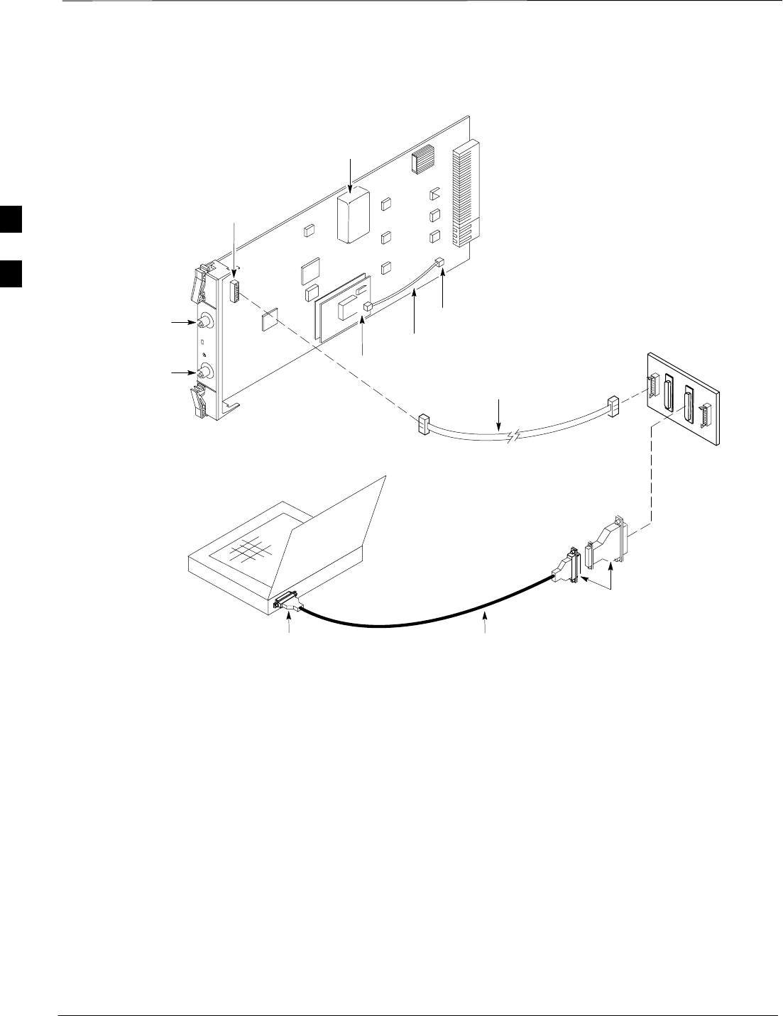
Establishing an MMI
Communication Session
For those procedures that require MMI communications between the
LMF and BTS FRUs, follow the procedure in Table 3-18 to initiate the
communication session.
Table 3-18: Establishing MMI Communications
Step Action
1Connect the LMF computer to the equipment as detailed in the applicable procedure that requires
MMI communication session.
2Start the named HyperTerminal connection for MMI sessions by double clicking on its Windows
desktop shortcut.
NOTE
If a Windows desktop shortcut was not created for the MMI connection, access the connection from
the Windows Start menu by selecting:
Programs>Accessories>Hyperterminal>HyperTerminal><Named HyperTerminal Connection
(e.g., MMI Session).
3Once the connection window opens, establish MMI communication with the BTS FRU by pressing
the LMF computer Enter key until the prompt identified in the applicable procedure is obtained.
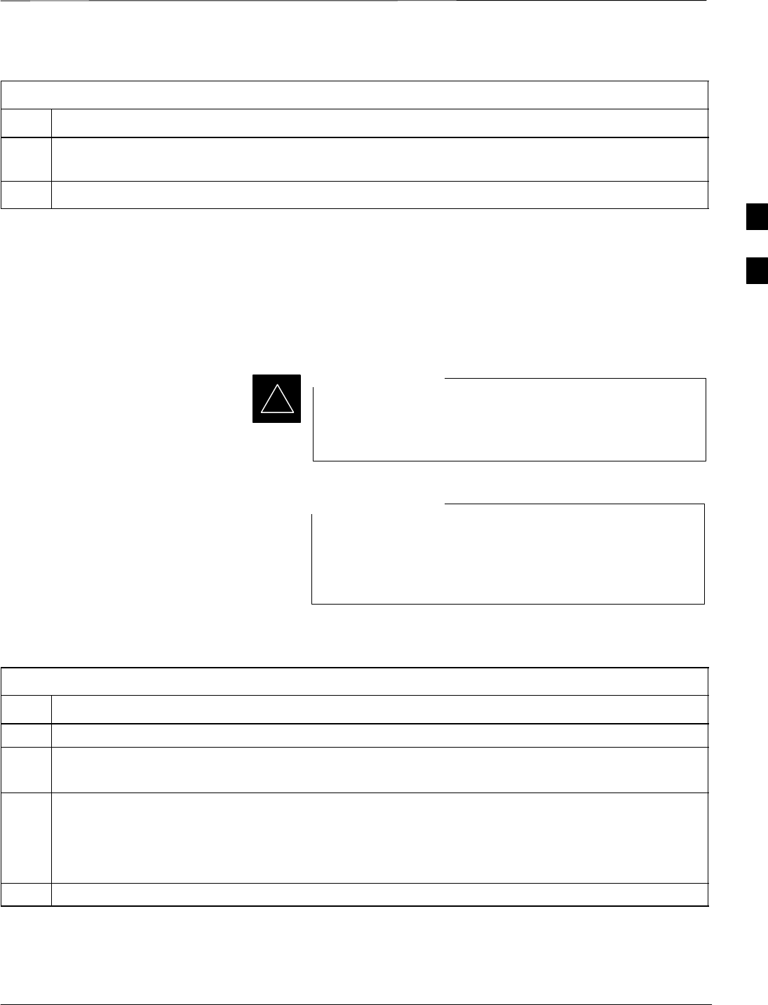
NULL MODEM
BOARD
(TRN9666A)
8–PIN TO 10–PIN
RS–232 CABLE (P/N
30–09786R01)
RS–232 CABLE
8–PIN
CDMA LMF
COMPUTER
To FRU MMI port
DB9–TO–DB25
ADAPTER
Figure 3-7: CDMA LMF Computer Common MMI Connections
COM1
OR
COM2
FW00687
3

Download the BTS
SCt4812ET BTS Optimization/ATP — CDMA LMF Jan 2002
3-38
Overview
Before a BTS can operate, each equipped device must contain device
initialization (ROM) code. ROM code is loaded in all devices during
manufacture, factory repair, or, for software upgrades, from the CBSC
using the DownLoad Manager (DLM). Device application (RAM) code
and data must be downloaded to each equipped device by the user before
the BTS can be made fully functional for the site where it is installed.
ROM Code
Downloading ROM code to BTS devices from the LMF is NOT routine
maintenance or a normal part of the optimization process. It is only
done in unusual situations where the resident ROM code release level in
the device is not compatible with the required release level of the site
operating software and the CBSC can not communicate with the BTS to
perform the download. An example would be a BTS loaded with R16.0
software where a GLI which is factory–loaded with R9.2.x or earlier
ROM code must be installed to replace a malfunctioning GLI.
Before ROM code can be downloaded from the LMF, the correct ROM
code file for each device to be loaded must exist on the LMF computer.
ROM code must be manually selected for download.
ROM code can be downloaded to a device that is in any state. After the
download is started, the device being downloaded will change to
OOS_ROM (blue). The device will remain OOS_ROM (blue) when the
download is completed. A compatible revision–level RAM code must
then be downloaded to the device. Compatible code loads for ROM and
RAM must be used for the device type to ensure proper performance.
The compatible device code release levels for the BSS software release
being used are listed in the Version Matrix section of the SCt CDMA
Release Notes (supplied on the tape or CD–ROM containing the BSS
software).
Procedures to load ROM code are located in Appendix J.
RAM Code
Before RAM code can be downloaded from the LMF, the correct RAM
code file for each device must exist on the LMF computer. RAM code
can be automatically or manually selected depending on the Device
menu item chosen and where the RAM code file for the device is stored
in the LMF file structure. The RAM code file will be selected
automatically if the file is in the <x>:\<lmf home
directory>\cdma\loads\n.n.n.n\code folder (where n.n.n.n is the
download code version number that matches the “NextLoad” parameter
of the CDF file). The RAM code file in the code folder must have the
correct hardware bin number for the device to be loaded.
RAM code can be downloaded to a device that is in any state. After the
download is started, the device being loaded will change to OOS_ROM
(blue). When the download is completed successfully, the device will
change to OOS_RAM (yellow).
3
Download the BTS – continued
Jan 2002 3-39
SCt4812ET BTS Optimization/ATP — CDMA LMF
When code is downloaded to an MGLI or GLI, the LMF automatically
also downloads data and then enables the MGLI. When enabled, the
MGLI will change to INS_ACT (bright green). A redundant GLI will
not be automatically enabled and will remain OOS_RAM (yellow).
When the redundant GLI is manually commanded to enable through the
LMF, it will change state to INS_SBY (olive green).
For non–GLI devices, data must be downloaded after RAM code is
downloaded. To download data, the device state must be OOS_RAM
(yellow).
The devices to be loaded with RAM code and data are:
SMaster Group Line Interface (MGLI)
SRedundant GLI
SClock Synchronization Module (CSM) (Only if new revision code
must be loaded)
SMulti Channel CDMA (MCC24E, MCC8E, or MCC–1X) cards
SBroadband Transceiver (BBX2 or BBX–1X) cards
SRFDS Test Subscriber Interface Card (TSIC) or RFDS–1X RFDS
PROCessor (RPROC) card, if RFDS is installed
The MGLI must be successfully downloaded with RAM
code and data, and in INS_ACT (bright green) status
before downloading any other device. The RAM code
download process for an MGLI automatically downloads
data and then enables the MGLI.
IMPORTANT
*
Verify GLI ROM Code Loads
Devices should not be loaded with a RAM code version which is not
compatible with the ROM code with which they are loaded. Before
downloading RAM code and data to the processor cards, follow the
procedure in Table 3-19 to verify the GLI devices are loaded with the
correct ROM code for the software release used by the BSS.
Prerequisite
Identify the correct GLI ROM code load for the software release being
used on the BSS by referring to the Version Matrix section of the
SCt CDMA Release Notes (supplied on the tape or CD–ROM
containing the BSS software).
Table 3-19: Verify GLI ROM Code Loads
Step Action
1If it has not already been done, start a GUI LMF session and log into the BTS ( refer to Table 3-14).
2Select all GLI devices by clicking on them, and select Device > Status from the BTS menu bar.
. . . continued on next page
3

Download the BTS – continued
SCt4812ET BTS Optimization/ATP — CDMA LMF Jan 2002
3-40
Table 3-19: Verify GLI ROM Code Loads
Step Action
3In the status report window which opens, note the number in the ROM Ver column for each GLI2.
4If the ROM code loaded in the GLIs is not the correct one for the software release being used on the
BSS, log out of the BTS, disconnect the LMF computer, reconnect the span lines as described in
Table 5-6, and have the CBSC download the correct ROM code version to the BTS devices.
5When the GLIs have the correct ROM load for the software release being used, be sure the span lines
are disabled as outlined in Table 3-2 and proceed to downloading RAM code and data.
Download RAM Code and Data
to MGLI and GLI Follow the steps outlined in Table 3-20 to download the RAM code and
data to the MGLI and other installed GLI devices.
Prerequisites
SPrior to performing these procedures, ensure a code file exists for each
of the devices to be loaded (refer to Table 3-3).
SThe LMF computer is connected to the BTS (refer toTable 3-6), and is
logged in using the GUI environment (refer to Table 3-14).
Table 3-20: Download and Enable MGLI and GLI Devices
Step Action
1Be sure the LMF will use the correct software release for code and data downloads by performing the
following steps:
1a –Click on Util in the BTS menu bar, and select Tools > Update NextLoad > CDMA from the
pull–down menus.
1b –Click on the BTS to be loaded.
–– The BTS will be highlighted.
1c –Click the button next to the correct code version for the software release being used.
–– A black dot will appear in the button circle.
1d –Click Save.
1e –Click OK to close each of the advisory boxes which appear.
2Prepare to download code to the MGLI by clicking on the device.
3 Click Device in the BTS menu bar, and select Download > Code/Data in the pull–down menus.
–A status report is displayed confirming change in the device(s) status.
4 Click OK to close the status window.
–The MGLI will automatically be downloaded with data and enabled.
. . . continued on next page
3
Download the BTS – continued
Jan 2002 3-41
SCt4812ET BTS Optimization/ATP — CDMA LMF
Table 3-20: Download and Enable MGLI and GLI Devices
Step Action
5Once the MGLI is enabled, load and enable additional installed GLIs by clicking on the devices and
repeating steps 3 and 4.
6 Click OK to close the status window for the additional GLI devices.
Download RAM Code and Data
to Non–GLI Devices
Downloads to non–GLI devices can be performed individually for each
device or all installed devices can be downloaded with one action. RAM
code and data are downloaded to non–GLI devices in separate steps.
CSM devices are RAM code–loaded at the factory. RAM
code is downloaded to CSMs only if a newer software
version needs to be loaded.
IMPORTANT
*
When downloading to multiple devices, the download may
fail for some of the devices (a time–out occurs). These
devices can be loaded individually after completing the
multiple download.
NOTE
Follow the steps in Table 3-21 to download RAM code and data to
non–GLI devices.
Table 3-21: Download RAM Code and Data to Non–GLI Devices
Step Action
1Select the target CSM, MCC, and/or BBX device(s) by clicking on them.
2 Click Device in the BTS menu bar, and select Download > Code/Data in the pull–down menus.
–A status report is displayed that shows the results of the download for each selected device.
3Click OK to close the status report window when downloading is completed.
NOTE
After a BBX, CSM, or MCC device is successfully loaded with RAM code and has changed to the
OOS_RAM state (yellow), the status LED should be rapidly flashing GREEN.
4To download data, select the target CSM, MCC and/or BBX device(s).
. . . continued on next page
3

Download the BTS – continued
SCt4812ET BTS Optimization/ATP — CDMA LMF Jan 2002
3-42
Table 3-21: Download RAM Code and Data to Non–GLI Devices
Step Action
5 Click Device in the BTS menu bar, and select select Download > Data in the pull–down menus.
–A status report is displayed showing the results of the download for each selected device.
6 Click OK to close the status report window when downloading is completed.
Select CSM Clock Source
A CSM can one of have three different clock sources. The Select CSM
Source function can be used to select the clock source for each of the
three inputs. This function is only used if the clock source for a CSM
needs to be changed. The Clock Source function provides the following
clock source options.
SLocal GPS
SRemote GPS
SHSO (only for source 2 & 3)
SHSOX (only for source 2 & 3)
SLFR (only for source 2 & 3)
S10 MHz (only for source 2 & 3)
SNONE (only for source 2 & 3)
Prerequisites
MGLI=INS_ACT, CSM= OOS_RAM or INS_ACT
Table 3-22: Select CSM Clock Source
Step Action
1Select the applicable CSM(s).
2Click on the Device menu.
3Click on the CSM/MAWI menu item.
4Click on the Select Clock Source menu item. A clock source selection window is displayed.
5Select the applicable clock source in the Clock Reference Source pick lists. Uncheck the related
check box if you do not want the displayed pick list item to be used.
6Click on the OK button. A status report window is displayed showing the results of the selection
action.
7Click on the OK button to close the status report window.
Enable CSMs
Each BTS CSM system features two CSM boards per site. In a typical
operation, the primary CSM locks its Digital Phase Locked Loop
(DPLL) circuits to GPS signals. These signals are generated by either an
3
Download the BTS – continued
Jan 2002 3-43
SCt4812ET BTS Optimization/ATP — CDMA LMF
on–board GPS module (RF–GPS) or a remote GPS receiver (R–GPS).
The CSM2 card is required when using the R–GPS. The GPS receiver
(mounted on CSM 1) is used as the primary timing reference and
synchronizes the entire cellular system. CSM 2 provides redundancy (but
does not have a GPS receiver).
The BTS may be equipped with a LORAN–C LFR, HSO, or external 10
MHz Rubidium source which the CSM can use as a secondary timing
reference. The HSOX is used for expansion frames. In all cases, the
CSM monitors and determines what reference to use at a given time.
For RF–GPS, verify the CSM configured with the GPS
receiver “daughter board” is installed in the frame’s CSM 1
slot before continuing.
IMPORTANT
*
Follow the steps outlined in Table 3-23 to enable the CSMs installed in
the C–CCP shelves.
Table 3-23: Enable CSMs
Step Action
1Click on the target CSM.
From the Device pull down, select Enable.
NOTE
If equipped with two CSMs, enable CSM–2 first
A status report is displayed confirming change in the device(s) status.
Click OK to close the status report window.
NOTE
FAIL may be shown in the status table for enable action. If Waiting For Phase Lock is shown in the
Description field, the CSM changes to the Enabled state after phase lock is achieved.
CSM 1 houses the GPS receiver. The enable sequence can take up to one hour (see below).
* IMPORTANT
The GPS satellite system satellites are not in a geosynchronous orbit and are maintained and operated
by the United States Department of Defense (D.O.D.). The D.O.D. periodically alters satellite orbits;
therefore, satellite trajectories are subject to change. A GPS receiver that is INS contains an “almanac”
that is updated periodically to take these changes into account.
If a GPS receiver has not been updated for a number of weeks, it may take up to an hour for the GPS
receiver “almanac” to be updated.
Once updated, the GPS receiver must track at least four satellites and obtain (hold) a 3–D position fix
for a minimum of 45 seconds before the CSM will come in service. (In some cases, the GPS receiver
needs to track only one satellite, depending on accuracy mode set during the data load).
. . . continued on next page
3
Download the BTS – continued
SCt4812ET BTS Optimization/ATP — CDMA LMF Jan 2002
3-44
Table 3-23: Enable CSMs
Step Action
2
NOTE
If equipped with two CSMs, CSM–1 should be bright green (INS–ACT) and CSM–2 should be dark
green (INS–STY)
If more than an hour has passed, refer to CSM Verification, see Figure 3-8 and Table 3-26 to determine
the cause.
NOTE
After the CSMs have been successfully enabled, observe the PWR/ALM LEDs are steady green
(alternating green/red indicates the card is in an alarm state).
Enable MCCs
This procedure configures the MCC and sets the “TX fine adjust”
parameter. The “TX fine adjust” parameter is not a transmit gain setting,
but a timing adjustment that compensates for the processing delay in the
BTS (approximately 3 mS).
Follow the steps outlined in Table 3-24 to enable the MCCs installed in
the C–CCP shelves.
The MGLI and CSM must be downloaded and enabled,
before downloading and enabling the MCC.
IMPORTANT
*
Table 3-24: Enable MCCs
Step Action
1Click on the target MCC(s) or from the Select pull down menu choose MCCs.
2From the Device menu, select Enable
A status report is displayed confirming change in the device(s) status.
3 Click OK to close the status report window.
3

CSM System Time – GPS & LFR/HSO Verification
Jan 2002 3-45
SCt4812ET BTS Optimization/ATP — CDMA LMF
Clock Synchronization
Manager System Time
The primary function of the Clock Synchronization Manager (CSM)
boards (slots 1 and 2) is to maintain CDMA system time. The CSM in
slot 1 is the primary timing source while slot 2 provides redundancy.
The CSM2 card (CSM second generation) is required when using the
remote GPS receiver (R–GPS). R–GPS uses a GPS receiver in the
antenna head that has a digital output to the CSM2 card. CSM2 can have
a daughter card as a local GPS receiver to support an RF–GPS signal.
The CSM2 switches between the primary and redundant units (slots 1
and 2) upon failure or command. CDMA Clock Distribution Cards
(CCDs) buffer and distribute even–second reference and 19.6608 MHz
clocks. CCD 1 is married to CSM 1 and CCD 2 is married to CSM 2. A
failure on CSM 1 or CCD 1 cause the system to switch to redundant
CSM 2 and CCD 2.
Each CSM2 board features an ovenized, crystal oscillator that provides
19.6608 MHz clock, even second pulse, and 3 MHz referenced to the
selected synchronization source (see Table 3-26):
SGPS: local/RF–GPS or remote/R–GPS
SLORAN–C Frequency Receiver (LFR) or High Stability Oscillator
(HSO)
SExternal reference oscillator sources
Fault management has the capability of switching between the GPS
synchronization source and the LFR/HSO backup source in the event of
a GPS receiver failure on CSM 1. During normal operation, the CSM 1
board selects GPS as the primary source (see Table 3-26). The source
selection can also be overridden via the LMF or by the system software.
Synchronization between the primary and redundant CSM CCD pairs, as
well as the LFR or HSO back–up to GPS synchronization, increases
reliability.
LFR/HSO
The CSM handles the overall configuration and status monitoring
functions of the LFR/HSO. In the event of GPS failure, the LFR/HSO is
capable of maintaining synchronization initially established by the GPS
reference signal.
The LFR requires an active external antenna to receive LORAN RF
signals. Timing pulses are derived from this signal, which is
synchronized to Universal Time Coordinates (UTC) and GPS time. The
LFR can maintain system time indefinately after initial GPS lock.
3

CSM System Time – GPS & LFR/HSO Verification – continued
SCt4812ET BTS Optimization/ATP — CDMA LMF Jan 2002
3-46
The HSO is a high stability 10 MHz oscillator with the necessary
interface to the CSMs. The HSO is typically installed in those
geographical areas not covered by the LORAN–C system. Since the
HSO is a free–standing oscillator, system time can only be maintained
for 24 hours after 24 hours of GPS lock.
Upgrades and Expansions: LFR2/HSO2/HSOX
LFR2/HSO2 (second generation cards) both export a timing signal to the
expansion frames. The associated expansion frames require an
HSO–expansion (HSOX) whether the starter frame has an LFR2 or an
HSO2. The HSOX accepts input from the starter frame and interfaces
with the CSM cards in the expansion frame. LFR and LFR2 use the
same source code in source selection (see Table 3-26). HSO, HSO2, and
HSOX use the same source code in source selection (see Table 3-26).
Allow the base site and test equipment to warm up for
60 minutes after any interruption in oscillator power.
CSM board warm-up allows the oscillator oven
temperature and oscillator frequency to stabilize prior to
test. Test equipment warm-up allows the Rubidium
standard timebase to stabilize in frequency before any
measurements are made.
NOTE
3
CSM System Time – GPS & LFR/HSO Verification – continued
Jan 2002 3-47
SCt4812ET BTS Optimization/ATP — CDMA LMF
CSM Frequency Verification
The objective of this procedure is the initial verification of the CSM
boards before performing the RF path verification tests. Parts of this
procedure will be repeated for final verification after the overall
optimization has been completed.
Test Equipment Setup
(GPS & LFR/HSO Verification)
Follow the steps outlined in Table 3-25 to set up test equipment.
Table 3-25: Test Equipment Setup (GPS & LFR/HSO Verification)
Step Action
1a For local GPS (RF–GPS): Verify a CSM board with a GPS receiver is installed in primary CSM slot 1
and that CSM–1 is INS.
NOTE
This is verified by checking the board ejectors for kit number SGLN1145 on the board in slot 1.
1b For Remote GPS (RGPS):Verify a CSM2 board is installed in primary slot 1 and that CSM–1 is INS.
NOTE
This is verified by checking the board ejectors for kit number SGLN4132ED or later.
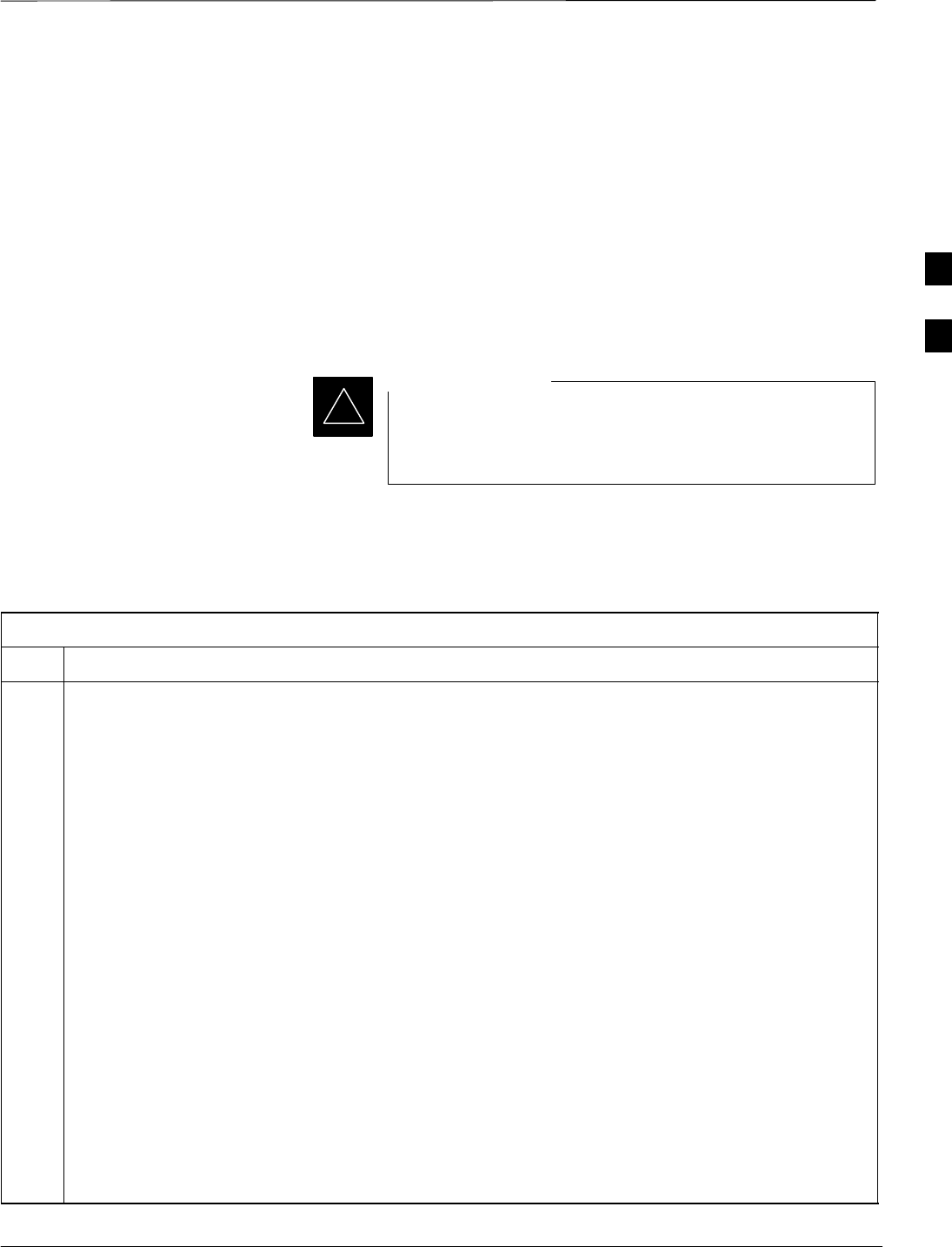
2Remove CSM–2 (if installed) and connect a serial cable from the LMF COM 1 port (via null modem
board) to the MMI port on CSM–1 (see Figure 3-8).
3Reinstall CSM–2.
4Start an MMI communication session with CSM–1 by using the Windows desktop shortcut icon (see
Table 3-5)
NOTE
The LMF program must be running when a Hyperterminal session is started.
5When the terminal screen appears press the Enter key until the CSM> prompt appears.
Connect GPS antenna to the (GPS) RF connector ONLY.
Damage to the GPS antenna and/or receiver can result if
the GPS antenna is inadvertently connected to any other
RF connector.
CAUTION
3
CSM System Time – GPS & LFR/HSO Verification – continued
SCt4812ET BTS Optimization/ATP — CDMA LMF Jan 2002
3-48
NULL MODEM
BOARD
(TRN9666A)
RS–232 SERIAL
MODEM CABLE
DB9–TO–DB25
ADAPTER
COM1
LMF
NOTEBOOK
Figure 3-8: CSM MMI Terminal Connection
FW00372
CSM board shown
removed from frame
19.6 MHZ TEST
POINT REFERENCE
(NOTE 1)
EVEN SECOND
TICK TEST POINT
REFERENCE
GPS RECEIVER
ANTENNA INPUT
GPS RECEIVER
MMI SERIAL
PORT
ANTENNA COAX
CABLE
REFERENCE
OSCILLATOR
9–PIN TO 9–PIN
RS–232 CABLE
NOTES:
1. One LED on each CSM:
Green = IN–SERVICE ACTIVE
Fast Flashing Green = OOS–RAM
Red = Fault Condition
Flashing Green & Red = Fault
GPS Initialization/Verification
Follow the steps outlined in Table 3-26 to connect to CSM–1 installed in
the C–CCP shelf, verifying that it is functioning normally.
3

CSM System Time – GPS & LFR/HSO Verification – continued
Jan 2002 3-49
SCt4812ET BTS Optimization/ATP — CDMA LMF
Table 3-26: GPS Initialization/Verification
Step Action
1To verify that Clock alarms (0000), Dpll is locked and has a reference source, and
GPS self test passed messages are displayed within the report, issue the following MMI
command
bstatus
–Observe the following typical response:
CSM Status INS:ACTIVE Slot A Clock MASTER.
Clock Alarms (0000):
DPLL is locked and has a reference source.
GPS receiver self test result: passed
Time since reset 0:33:11, time since power on: 0:33:11
2Enter the following command at the CSM> prompt to display the current status of the Loran and the
GPS receivers.
sources
–Observe the following typical response for systems equipped with LFR:
N Source Name Type TO Good Status Last Phase Target Phase Valid
–––––––––––––––––––––––––––––––––––––––––––––––––––––––––––––––––––––––––
0LocalGPS Primary 4 YES Good 00Yes
1 LFR CHA Secondary 4 YES Good –2013177 –2013177 Yes
2 Not Used
Current reference source number: 0
–Observe the following typical response for systems equipped with HSO:
Num Source Name Type TO Good Status Last Phase Target Phase Valid
––––––––––––––––––––––––––––––––––––––––––––––––––––––––––––––––––––––––––––
0 Local GPS Primary 4 Yes Good 3 0 Yes
1HSO Backup 4 No N/A timed–out* Timed–out* No
*NOTE “Timed–out” should only be displayed while the HSO is warming up. “Not–Present” or
“Faulty” should not be displayed. If the HSO does not appear as one of the sources, then configure the
HSO as a back–up source by entering the following command at the CSM> prompt:
ss 1 12
After a maximum of 15 minutes, the Rubidium oscillator should reach operational temperature and the
LED on the HSO should now have changed from red to green. After the HSO front panel LED has
changed to green, enter sources <cr> at the CSM> prompt. Verify that the HSO is now a valid
source by confirming that the bold text below matches the response of the “sources” command.
The HSO should be valid within one (1) minute, assuming the DPLL is locked and the HSO rubidium
oscillator is fully warmed.
Num Source Name Type TO Good Status Last Phase Target Phase Valid
––––––––––––––––––––––––––––––––––––––––––––––––––––––––––––––––––––––––––––
0 Local GPS Primary 4 Yes Good 3 0 Yes
1HSO Backup 4 Yes N/A xxxxxxxxxx xxxxxxxxxx Yes
. . . continued on next page
3

CSM System Time – GPS & LFR/HSO Verification – continued
SCt4812ET BTS Optimization/ATP — CDMA LMF Jan 2002
3-50
Table 3-26: GPS Initialization/Verification
Step Action
3HSO information (underlined text above, verified from left to right) is usually the #1 reference source.
If this is not the case, have the OMCR determine the correct BTS timing source has been identified in
the database by entering the display bts csmgen command and correct as required using the edit
csm csmgen refsrc command.
* IMPORTANT
If any of the above mentioned areas fail, verify:
–If LED is RED, verify that HSO had been powered up for at least 5 minutes. After oscillator
temperature is stable, LED should go GREEN Wait for this to occur before continuing !
–If “timed out” is displayed in the Last Phase column, suspect the HSO output buffer or oscillator
is defective
–Verify the HSO is FULLY SEATED and LOCKED to prevent any possible board warpage
4Verify the following GPS information (underlined text above):
–GPS information is usually the 0 reference source.
–At least one Primary source must indicate “Status = good” and “Valid = yes” to bring site up.
. . . continued on next page
3

CSM System Time – GPS & LFR/HSO Verification – continued
Jan 2002 3-51
SCt4812ET BTS Optimization/ATP — CDMA LMF
Table 3-26: GPS Initialization/Verification
Step Action
5Enter the following command at the CSM> prompt to verify that the GPS receiver is in tracking mode.
gstatus
–Observe the following typical response:
24:06:08 GPS Receiver Control Task State: tracking satellites.
24:06:08 Time since last valid fix: 0 seconds.
24:06:08
24:06:08 Recent Change Data:
24:06:08 Antenna cable delay 0 ns.
24:06:08 Initial position: lat 117650000 msec, lon –350258000 msec, height 0 cm (GPS)
24:06:08 Initial position accuracy (0): estimated.
24:06:08
24:06:08 GPS Receiver Status:
24:06:08 Position hold: lat 118245548 msec, lon –350249750 msec, height 20270 cm
24:06:08 Current position: lat 118245548 msec, lon –350249750 msec, height 20270 cm
(GPS)
24:06:08 8 satellites tracked, receiving 8 satellites, 8 satellites visible.
24:06:08 Current Dilution of Precision (PDOP or HDOP): 0.
24:06:08 Date & Time: 1998:01:13:21:36:11
24:06:08 GPS Receiver Status Byte: 0x08
24:06:08 Chan:0, SVID: 16, Mode: 8, RSSI: 148, Status: 0xa8
24:06:08 Chan:1, SVID: 29, Mode: 8, RSSI: 132, Status: 0xa8
24:06:08 Chan:2, SVID: 18, Mode: 8, RSSI: 121, Status: 0xa8
24:06:08 Chan:3, SVID: 14, Mode: 8, RSSI: 110, Status: 0xa8
24:06:08 Chan:4, SVID: 25, Mode: 8, RSSI: 83, Status: 0xa8
24:06:08 Chan:5, SVID: 3, Mode: 8, RSSI: 49, Status: 0xa8
24:06:08 Chan:6, SVID: 19, Mode: 8, RSSI: 115, Status: 0xa8
24:06:08 Chan:7, SVID: 22, Mode: 8, RSSI: 122, Status: 0xa8
24:06:08
24:06:08 GPS Receiver Identification:
24:06:08 COPYRIGHT 1991–1996 MOTOROLA INC.
24:06:08 SFTW P/N # 98–P36830P
24:06:08 SOFTWARE VER # 8
24:06:08 SOFTWARE REV # 8
24:06:08 SOFTWARE DATE 6 AUG 1996
24:06:08 MODEL # B3121P1115
24:06:08 HDWR P/N # _
24:06:08 SERIAL # SSG0217769
24:06:08 MANUFACTUR DATE 6B07
24:06:08 OPTIONS LIST IB
24:06:08 The receiver has 8 channels and is equipped with TRAIM.
6Verify the following GPS information (shown above in underlined text):
–At least 4 satellites are tracked, and 4 satellites are visible.
–GPS Receiver Control Task State is “tracking satellites”. Do not continue until this occurs!
–Dilution of Precision indication is not more that 30.
Record the current position base site latitude, longitude, height and height reference (height reference
to Mean Sea Level (MSL) or GPS height (GPS). (GPS = 0 MSL = 1).
. . . continued on next page
3
CSM System Time – GPS & LFR/HSO Verification – continued
SCt4812ET BTS Optimization/ATP — CDMA LMF Jan 2002
3-52
Table 3-26: GPS Initialization/Verification
Step Action
7If steps 1 through 6 pass, the GPS is good.
* IMPORTANT
If any of the above mentioned areas fail, verify that:
–If Initial position accuracy is “estimated” (typical), at least 4 satellites must be tracked and
visible (1 satellite must be tracked and visible if actual lat, log, and height data for this site has
been entered into CDF file).
–If Initial position accuracy is “surveyed,” position data currently in the CDF file is assumed to be
accurate. GPS will not automatically survey and update its position.
–The GPS antenna is not obstructed or misaligned.
–GPS antenna connector center conductor measureS approximately +5 Vdc with respect to the
shield.
–There is no more than 4.5 dB of loss between the GPS antenna OSX connector and the BTS frame
GPS input.
–Any lightning protection installed between GPS antenna and BTS frame is installed correctly.
8Enter the following commands at the CSM> prompt to verify that the CSM is warmed up and that GPS
acquisition has taken place.
debug dpllp
Observe the following typical response if the CSM is not warmed up (15 minutes from application of
power) (If warmed–up proceed to step 9)
CSM>DPLL Task Wait. 884 seconds left.
DPLL Task Wait. 882 seconds left.
DPLL Task Wait. 880 seconds left. ...........etc.
NOTE
The warm command can be issued at the MMI port used to force the CSM into warm–up, but the
reference oscillator will be unstable.
9Observe the following typical response if the CSM is warmed up.
c:17486 off: –11, 3, 6 TK SRC:0 S0: 3 S1:–2013175,–2013175
c:17486 off: –11, 3, 6 TK SRC:0 S0: 3 S1:–2013175,–2013175
c:17470 off: –11, 1, 6 TK SRC:0 S0: 1 S1:–2013175,–2013175
c:17486 off: –11, 3, 6 TK SRC:0 S0: 3 S1:–2013175,–2013175
c:17470 off: –11, 1, 6 TK SRC:0 S0: 1 S1:–2013175,–2013175
c:17470 off: –11, 1, 6 TK SRC:0 S0: 1 S1:–2013175,–2013175
10 Verify the following GPS information (underlined text above, from left to right):
–Lower limit offset from tracked source variable is not less than –60 (equates to 3 µs limit).
–Upper limit offset from tracked source variable is not more than +60 (equates to 3 µs limit).
–TK SRC: 0 is selected, where SRC 0 = GPS.
11 Enter the following commands at the CSM> prompt to exit the debug mode display.
debug dpllp
3

CSM System Time – GPS & LFR/HSO Verification – continued
Jan 2002 3-53
SCt4812ET BTS Optimization/ATP — CDMA LMF
LORAN–C
Initialization/Verification
Table 3-27: LORAN–C Initialization/Verification
Step Action Note
1At the CSM> prompt, enter lstatus <cr> to verify that the LFR is in tracking
mode. A typical response is:
CSM> lstatus <cr>
LFR St ti St t
LFR Station Status:
Clock coherence: 512 >
5930M 51/60 dB 0 S/N Flag:
5930X 52/64 dn –1 S/N Flag:
5990 47/55 dB –6 S/N Flag:
7980M 62/66 dB 10 S/N Fl
This must be greater
than 100 before LFR
becomes a valid source.
7980M 62/66 dB 10 S/N Flag:
7980W 65/69 dB 14 S/N Flag: . PLL Station . >
7980X 48/54 dB –4 S/N Flag:
7980Y 46/58 dB –8 S/N Flag:E
7980Z 60/67 dB 8 S/N Flag:
8290M 50/65 dB 0 S/N Flag
This shows the LFR is
locked to the selected
PLL station.
8290M 50/65 dB 0 S/N Flag:
8290W 73/79 dB 20 S/N Flag:
8290W 58/61 dB 6 S/N Flag:
8290W 58/61 dB 6 S/N Flag:
8970M 89/95 dB 29 S/N Flag:
8970W 62/66 dB 10 S/N Flag:
8970X 73/79 dB 22 S/N Flag:
8970X 73/79 dB 22 S/N Fl
ag:
8970Y 73/79 dB 19 S/N Flag:
8970Z 62/65 dB 10 S/N Flag:
9610M 62/65 dB 10 S/N Fl
g
9610M 62/65 dB 10 S/N Flag:
9610V 58/61 dB 8 S/N Flag:
9610W 47
/
49 dB –4S
/
N Fla
g
:E
9610W 47/49 dB –4 S/N Flag:E
9610X 46/57 dB –5 S/N Flag:E
9610Y 48/54 dB –5 S/N Flag:E
9610Z 65/69 dB 12 S/N Flag
9610Z 65/69 dB 12 S/N Flag:
9940M 50/53 dB –1 S/N Flag:S
9940W 49/56 dB –4 S/N Flag:E
9940W 49/56 dB 4 S/N Flag:E
9940Y 46/50 dB–10 S/N Flag:E
9960M 73/79 dB 22 S/N Flag:
9960W 51/60 dB 0 S/N Flag:
9960W 51/60 dB 0 S/N Fl
ag:
9960X 51/63 dB –1 S/N Flag:
9960Y 59/67 dB 8 S/N Flag:
9960Z 89/96 dB 29 S/N Fl
9960Z 89/96 dB 29 S/N Flag:
LFR Task State: lfr locked to station 7980W
LFR Recent Change Data:
Search List: 5930 5990 7980 8290 8970 9940 9610 9960 >
PLL GRI: 7980W
LFR Master, reset not needed, not the reference source.
CSM>
This search list and PLL
data must match the
configuration for the
geographical location
of the cell site.
. . . continued on next page
3

CSM System Time – GPS & LFR/HSO Verification – continued
SCt4812ET BTS Optimization/ATP — CDMA LMF Jan 2002
3-54
Table 3-27: LORAN–C Initialization/Verification
Step NoteAction
2Verify the following LFR information (highlighted above in boldface type):
–Locate the “dot” that indicates the current phase locked station assignment (assigned by MM).
–Verify that the station call letters are as specified in site documentation as well as M X Y Z
assignment.
–Verify the S/N ratio of the phase locked station is greater than 8.
3At the CSM> prompt, enter sources <cr> to display the current status of the the LORAN receiver.
–Observe the following typical response.
Num Source Name Type TO Good Status Last Phase Target Phase Valid
––––––––––––––––––––––––––––––––––––––––––––––––––––––––––––––––––––––––––––
0 Local GPS Primary 4 Yes Good –3 0 Yes
1 LFR ch A Secondary 4 Yes Good –2013177 –2013177 Yes
2 Not used
Current reference source number: 1
4LORAN LFR information (highlighted above in boldface type) is usually the #1 reference source
(verified from left to right).
* IMPORTANT
If any of the above mentioned areas fail, verify:
–The LFR antenna is not obstructed or misaligned.
–The antenna pre–amplifier power and calibration twisted pair connections are intact and < 91.4 m
(300 ft) in length.
–A dependable connection to suitable Earth Ground is in place.
–The search list and PLL station for cellsite location are correctly configured .
NOTE
LFR functionality should be verified using the “source” command (as shown in Step 3). Use the
underlined responses on the LFR row to validate correct LFR operation.
5Close the hyperterminal window.
3

Test Equipment Set–up
Jan 2002 3-55
SCt4812ET BTS Optimization/ATP — CDMA LMF
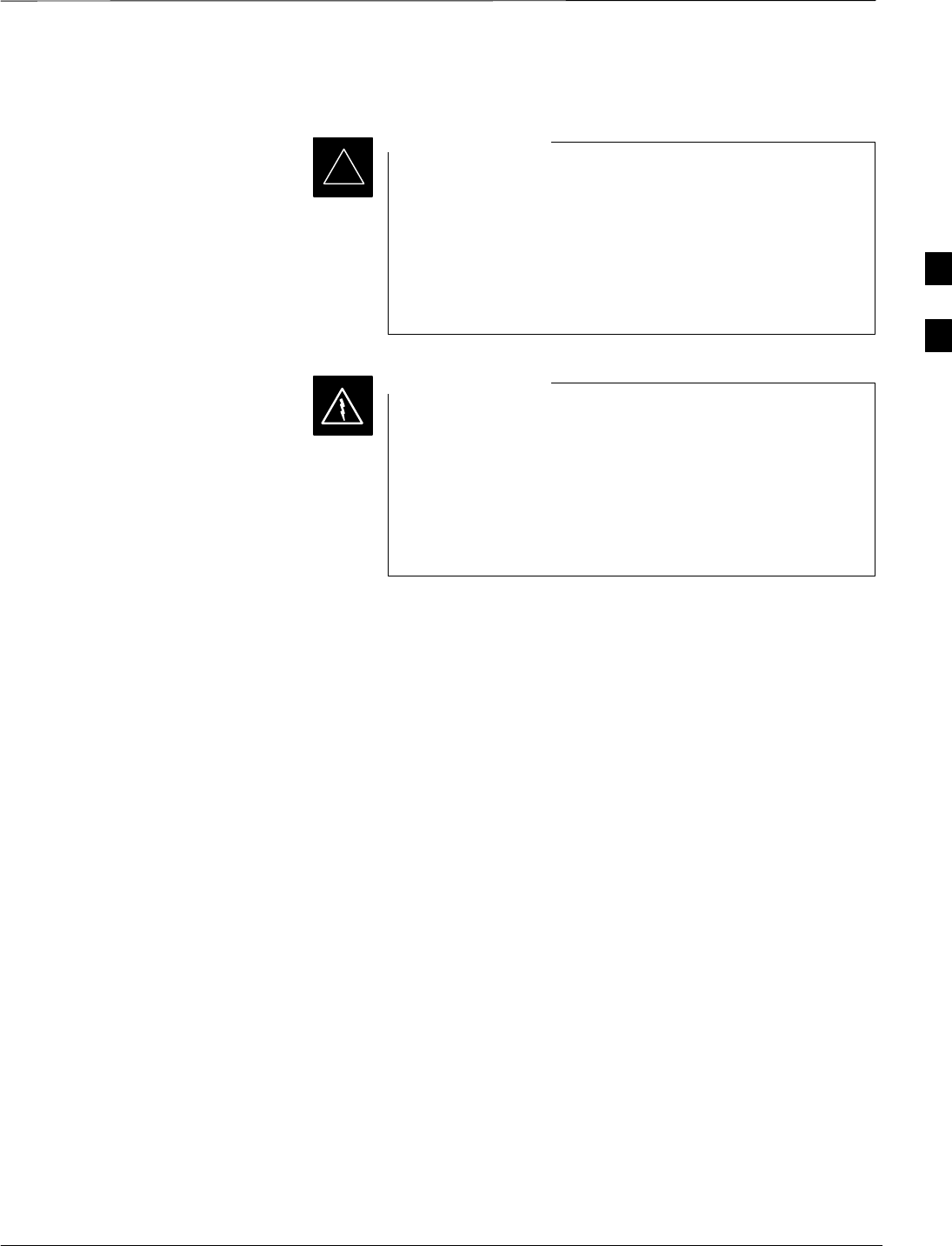
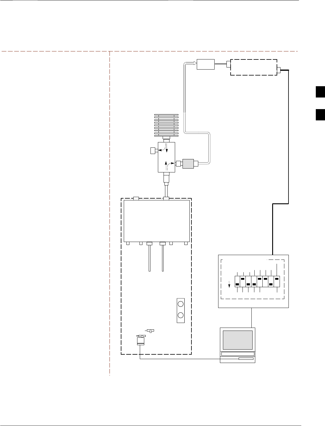
Connecting Test Equipment to
the BTS
The following test equipment is required to perform calibration and ATP
tests:
SLMF
SCommunications system analyzer model supported by the LMF
SPower meter model supported by the LMF (required when using the
HP 8921A/600 and Advantest R3465 analyzers)
SNon–radiating transmit line termination load
SDirectional coupler and in–line attenuator
SRF cables and adapters
Refer to Table 3-28 and Table 3-29 for an overview of connections for
test equipment currently supported by the LMF. In addition, see the
following figures:
SFigure 3-9 and Figure 3-10 show cable calibration test setup.
SFigure 3-11, Figure 3-12 and Figure 3-14 show the test set
connections for TX calibration.
SFigure 3-14 and Figure 3-15 show test set connections for IS–95 A/B
optimization/ATP tests
SFigure 3-16 through Figure 3-19 shows test set connections for
IS–95 A/B/C optimization/ATP tests.
SFigure 3-20 and Figure 3-21 show typical TX and RX ATP setup with
a directional coupler (shown with and without RFDS).
Test Equipment GPIB Address
Settings
All test equipment is controlled by the LMF through an IEEE–488/GPIB
bus. To communicate on the bus, each piece of test equipment must have
a GPIB address set which the LMF will recognize. The standard address
settings used by the LMF for the various types of test equipment items
are as follows:
SSignal generator address: 1
SPower meter address: 13
SCommunications system analyzer: 18
Using the procedures included in the Setting GPIB Addresses section of
Appendix I, verify and, if necessary, change the GPIB address of each
piece of test equipment used to match the above.
Supported Test Sets
To prevent damage to the test equipment, all TX test
connections must be through the directional coupler and
in-line attenuator as shown in the test setup illustrations.
CAUTION
3

Test Equipment Set–up – continued
SCt4812ET BTS Optimization/ATP — CDMA LMF Jan 2002
3-56
IS–95 A/B Testing
Optimization and ATP testing for IS–95A/B sites or carriers may be
performed using one of the following test equipment:
SCyberTest
SAdvantest R3267 spectrum analyzer with R3562 signal generator and
HP–437B or Gigatronics Power Meter
SAgilent E4406A transmitter test set with E4432B signal generator
SAgilent 8935 series E6380A communications test set (formerly HP
8935)
SHewlett–Packard HP 8921 (with CDMA interface for 1.9 GHz PCS
Interface) and HP–437B or Gigatronics Power Meter
SSpectrum Analyzer (HP8594E) – optional
SRubidium Standard Timebase – optional
CDMA2000 1X Operation
Optimization and ATP testing for CDMA2000 1X sites or carriers may
be performed using the following test equipment:
SAdvantest R3267 spectrum analyzer with R3562 signal generator
SAgilent E4406A transmitter test set with E4432B signal generator
SAgilent 8935 series E6380A communications test set (formerly HP
8935) with option 200 or R2K and with E4432B signal generator for
1X FER
Test Equipment Preparation
See Appendix I for specific steps to prepare each type of test set and
power meter to perform calibration and ATP .
3
Test Equipment Set–up – continued
Jan 2002 3-57
SCt4812ET BTS Optimization/ATP — CDMA LMF
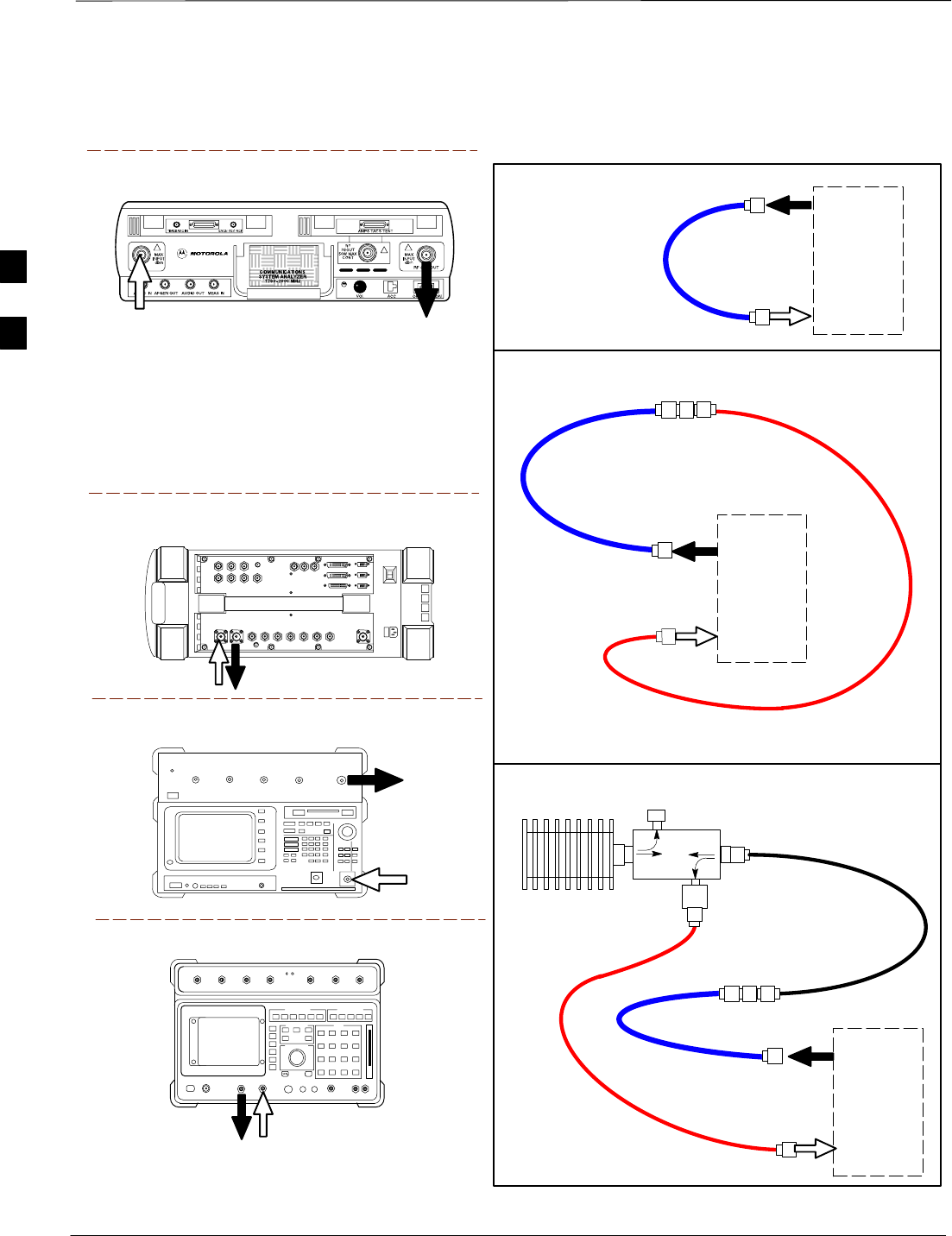
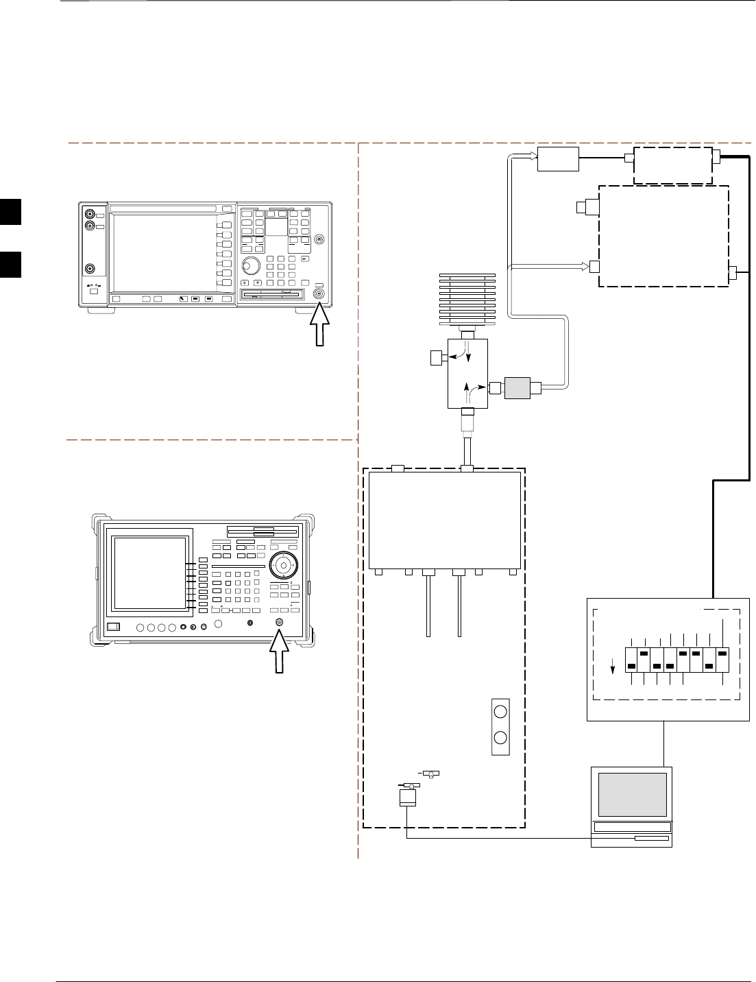
Test Equipment Connection
Charts
To use the following charts to identify necessary test equipment
connections, locate the communications system analyzer being used in
the COMMUNICATIONS SYSTEM ANALYZER columns, and read down
the column. Where a dot appears in the column, connect one end of the
test cable to that connector. Follow the horizontal line to locate the end
connection(s), reading up the column to identify the appropriate
equipment and/or BTS connector.
IS–95A/B–only Test Equipment Connections
Table 3-28 depicts the interconnection requirements for currently
available test equipment supporting IS–95A/B only which meets
Motorola standards and is supported by the LMF.
Table 3-28: IS–95A/B–only Test Equipment Interconnection
COMMUNICATIONS SYSTEM ANALYZER ADDITIONAL TEST EQUIPMENT
SIGNAL Cyber–Test Advantest
R3465 HP 8921A HP 8921
W/PCS Power
Meter GPIB
Interface LMF
Attenuator
&
Directional
Coupler BTS
EVEN SECOND
SYNCHRONIZATION EVEN
SEC REF EVEN SEC
SYNC IN
EVEN
SECOND
SYNC IN
EVEN
SECOND
SYNC IN
19.6608 MHZ
CLOCK TIME
BASE IN
CDMA
TIME BASE
IN
CDMA
TIME BASE
IN
CDMA
TIME BASE
IN
CONTROL
IEEE 488 BUS IEEE
488 GPIB GPIB SERIAL
PORT
HP–IB HP–IB
TX TEST
CABLES RF
IN/OUT INPUT
50WTX1–6
RF
IN/OUT RF
IN/OUT 20 DB
ATTEN. BTS
PORT
RX TEST
CABLES RF
GEN OUT RF OUT
50WRX1–6
DUPLEX
OUT RF OUT
ONLY
SYNC
MONITOR
FREQ
MONITOR
HP–IB
3
Test Equipment Set–up – continued
SCt4812ET BTS Optimization/ATP — CDMA LMF Jan 2002
3-58
CDMA2000 1X/IS–95A/B–capable Test Equipment
Connections
Table 3-29 depicts the interconnection requirements for currently
available test equipment supporting both CDMA 2000 1X and
IS–95A/B which meets Motorola standards and is supported by the
LMF.
Table 3-29: CDMA2000 1X/IS–95A/B Test Equipment Interconnection
COMMUNICATIONS SYSTEM
ANALYZER ADDITIONAL TEST EQUIPMENT
SIGNAL
Agilent
8935
(Option
200 or
R2K) Advantest
R3267 Agilent
E4406A
Agilent
E4432
Signal
Gen.
Advantest
R3562
Signal
Generator Power
Meter GPIB
Interface LMF
Attenuator
&
Directional
Coupler BTS
EVEN SECOND
SYNCHRONIZATION
EVEN
SECOND
SYNC IN EXT TRIG
IN
19.6608 MHZ
CLOCK EXT REF
IN MOD TIME
BASE IN
CONTROL
IEEE 488 BUS
10 MHZ
OUT
GP–IBHP–IB GP–IB GPIB SERIAL
PORT
GPIB GPIB
TX TEST
CABLES RF
IN/OUT INPUT
50 WTX1–6
20 DB
ATTEN. BTS
PORT
SYNC
MONITOR
FREQ
MONITOR
HP–IB
PATTERN
TRIG IN
EXT REF
IN
RF INPUT
50 W
RX TEST
CABLES RF OUT
50 W
DUPLEX
OUT RF OUTPUT
50 WRX1–6
10 MHZ 10 MHZ OUT
(SWITCHED) SYNTHE
REF IN
10 MHZ
IN
TRIGGER
IN
EXT TRIG
SIGNAL SOURCE
CONTROLLED
SERIAL I/O
SERIAL
I/O SERIAL
I/O
10 MHZ
REF OUT
* WHEN USED ALONE, THE AGILENT 8935 WITH OPTION 200 OR R2K SUPPORTS IS–95A/B RX TESTING BUT NOT 1X RX TESTING.
*
3
Test Equipment Set–up – continued
Jan 2002 3-59
SCt4812ET BTS Optimization/ATP — CDMA LMF
Equipment Warm-up
Warm-up BTS equipment for a minimum of 60 minutes
prior to performing the BTS optimization procedure. This
assures BTS stability and contributes to optimization
accuracy.
–Time spent running initial or normal power-up,
hardware/firmware audit, and BTS download counts
as warm-up time.
IMPORTANT
*
Before installing any test equipment directly to any BTS
TX OUT connector, verify there are no CDMA channels
keyed.
–At active sites, have the OMC-R/CBSC place the
antenna (sector) assigned to the BBX under test OOS.
Failure to do so can result in serious personal injury
and/or equipment damage.
WARNING
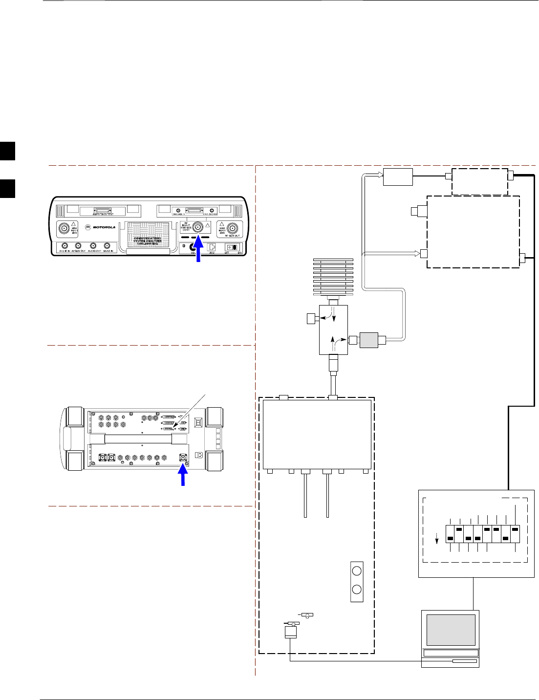
Automatic Cable Calibration
Set–up
Figure 3-9 and Figure 3-10 show the cable calibration setup for the test
sets supported by the LMF. The left side of the diagram depicts the
location of the input and output connectors of each test equipment item,
and the right side details the connections for each test. Table 3-33
provides a procedure for performing automatic cable calibration.
Manual Cable Calibration
If manual cable calibration is required, refer to the procedures in
Appendix F.
3
Test Equipment Set–up – continued
SCt4812ET BTS Optimization/ATP — CDMA LMF Jan 2002
3-60
Motorola CyberTest
Advantest Model R3465
RF OUT 50Ω
INPUT 50Ω
RF GEN OUTANT IN
SUPPORTED TEST SETS
100–WATT (MIN)
NON–RADIATING
RF LOAD
TEST
SET
A. SHORT CABLE CAL
SHORT
CABLE
B. RX TEST SETUP FOR TRDC
TEST
SET
C. TX TEST SETUP AND DRDC RX TEST SETUP
20 DB IN–LINE
ATTENUATOR
CALIBRATION SET UP
N–N FEMALE
ADAPTER
TX
CABLE
SHORT
CABLE
Note: The 30 dB directional coupler is not used
with the Cybertest test set. The TX cable is
connected directly to the Cybertest test set.
A 10dB attenuator must be used with the short test
cable for cable calibration with the CyberTest test
set. The 10dB attenuator is used only for the cable
calibration procedure, not with the test cables for
TX calibration and ATP tests.
TEST
SET
RX
CABLE
SHORT
CABLE
DIRECTIONAL
COUPLER
(30 DB)
N–N FEMALE
ADAPTER
50 Ω
ΤERM.
Figure 3-9: Cable Calibration Test Setup – CyberTest, Agilent 8935, Advantest R3465, and HP 8921A
Agilent 8935 Series E6380A
(formerly HP 8935)
DUPLEX
OUT
ANT
IN
Hewlett Packard Model HP 8921A
Note: For 800 MHZ only. The HP8921A cannot
be used to calibrate cables for PCS frequencies.
TX CABLE FOR
TX TEST CABLE
CALIBRATION
RX CABLE FOR
DRDC RX TEST
CABLE CALIBRATION
DUPLEX
OUT ANT
IN
3
Test Equipment Set–up – continued
Jan 2002 3-61
SCt4812ET BTS Optimization/ATP — CDMA LMF
TEST
SET
A. SHORT CABLE CAL
SHORT
CABLE
B. RX TEST SETUP FOR TRDC
CALIBRATION SET UP
TEST
SET
RX
CABLE
SHORT
CABLE
N–N FEMALE
ADAPTER
Figure 3-10: Cable Calibration Test Setup – Agilent E4406A/E4432B and Advantest R3267/R3562
SUPPORTED TEST SETS
INPUT 50 Ω
RF OUT
50 Ω
Advantest R3267 (Top) and R3562 (Bottom)
NOTE:
SYNTHE REF IN ON REAR OF SIGNAL GENERATOR IS
CONNECTED TO 10 MHZ OUT ON REAR OF SPECTRUM
ANALYZER
Agilent E4432B (Top) and E4406A (Bottom)
NOTE:
10 MHZ IN ON REAR OF SIGNAL GENERATOR IS CONNECTED TO
10 MHZ OUT (SWITCHED) ON REAR OF TRANSMITTER TESTER
(FIGURE F-5).
RF INPUT
50 Ω
RF OUTPUT
50 Ω
100–WATT (MIN)
NON–RADIATING
RF LOAD
TEST
SET
D. TX TEST SETUP AND DRDC RX TEST SETUP
20 DB IN–LINE
ATTENUATOR
N–N FEMALE
ADAPTER
TX
CABLE
SHORT
CABLE
DIRECTIONAL
COUPLER
(30 DB)
50 Ω
ΤERM.
TX CABLE FOR
TX TEST CABLE
CALIBRATION
RX CABLE FOR
DRDC RX TEST
CABLE CALIBRATION
3
Test Equipment Set–up – continued
SCt4812ET BTS Optimization/ATP — CDMA LMF Jan 2002
3-62
Set–up for TX Calibration
Figure 3-11 and Figure 3-12 show the test set connections for TX
calibration.
Motorola CyberTest
Agilent 8935 Series E6380A (formerly HP 8935)
TEST SETS TRANSMIT (TX) SET UP
FRONT PANEL
RF
IN/OUT
RF IN/OUT
HP–IB
TO GPIB
BOX
NOTE: THE 30 DB DIRECTIONAL COUPLER IS NOT USED WITH THE
CYBERTEST TEST SET. THE TX CABLE IS CONNECTED DIRECTLY
TO THE CYBERTEST TEST SET.
Figure 3-11: TX Calibration Test Setup – CyberTest (IS–95A/B) and
Agilent 8935 (IS–95A/B and CDMA2000 1X)
TO
MPC
TO LPA
TRUNKING
MODULE
RS232–GPIB
INTERFACE BOX
INTERNAL PCMCIA
ETHERNET CARD
GPIB
CABLE
UNIVERSAL TWISTED PAIR (UTP)
CABLE (RJ45 CONNECTORS)
RS232 NULL
MODEM
CABLE
S MODE
DATA FORMAT
BAUD RATE
GPIB ADRS G MODE
ON
BTS
INTERNAL
TX
CABLE
CDMA
LMF
DIP SWITCH SETTINGS
10BASET/
10BASE2
CONVERTER
LAN
B
LAN
A
GPIB
RF IN/OUT
RX
ANTENNA
CONNECTOR
FREQ
MONITOR
SYNC
MONITOR
CSM
INTERNAL
RX
CABLE
TX
ANT
CPLD
RX
BTS
CPLD
TRDC
TX
BTS
CPLD
RX
ANT
CPLD
TX
ANTENNA
CONNECTOR
COMMUNICATIONS
TEST SET
2O DB IN–LINE
ATTENUATOR
50 Ω
TERM
.
TX TEST
CABLE
DIRECTIONAL
COUPLER
(30 DB)
100–WATT (MIN.)
NON–RADIATING
RF LOAD
TX TEST
CABLE
* BLACK RECTANGLES
REPRESENT THE RAISED
PART OF SWITCHES
NOTE: IF BTS IS EQUIPPED
WITH DRDCS (DUPLEXED
RX/TX SIGNALS), CONNECT
THE TX TEST CABLE TO
THE DRDC ANTENNA
CONNECTOR.
POWER
METER
(OPTIONAL)*
POWER
SENSOR
* A POWER METER CAN BE USED IN
PLACE OF THE COMMUNICATIONS
TEST SET FOR TX CALIBRATION/
AUDIT
3
Test Equipment Set–up – continued
Jan 2002 3-63
SCt4812ET BTS Optimization/ATP — CDMA LMF
TEST SETS TRANSMIT (TX) SET UP
NOTE: THE HP8921A AND ADVANTEST
R3465 CANNOT BE USED FOR TX
CALIBRATION. A POWER METER MUST BE
USED.
Figure 3-12: TX Calibration Test Setup – Using Power Meter
TO
MPC
TO LPA
TRUNKING
MODULE
RS232–GPIB
INTERFACE BOX
INTERNAL PCMCIA
ETHERNET CARD
GPIB
CABLE
UNIVERSAL TWISTED PAIR (UTP)
CABLE (RJ45 CONNECTORS)
RS232 NULL
MODEM
CABLE
S MODE
DATA FORMAT
BAUD RATE
GPIB ADRS G MODE
ON
BTS
INTERNAL
TX
CABLE
CDMA
LMF
DIP SWITCH SETTINGS
10BASET/
10BASE2
CONVERTER
LAN
B
LAN
A
RX
ANTENNA
CONNECTOR
FREQ
MONITOR
SYNC
MONITOR
CSM
INTERNAL
RX
CABLE
TX
ANT
CPLD
RX
BTS
CPLD
TRDC
TX
BTS
CPLD
RX
ANT
CPLD
TX
ANTENNA
CONNECTOR
50 Ω
TERM
.
TX TEST
CABLE
DIRECTIONAL
COUPLER
(30 DB)
100–WATT (MIN.)
NON–RADIATING
RF LOAD
TX TEST
CABLE
* BLACK RECTANGLES
REPRESENT THE RAISED
PART OF SWITCHES
NOTE: IF BTS IS EQUIPPED
WITH DRDCS (DUPLEXED
RX/TX SIGNALS), CONNECT
THE TX TEST CABLE TO
THE DRDC ANTENNA
CONNECTOR.
POWER
SENSOR POWER METER
2O DB IN–LINE
ATTENUATOR
3
Test Equipment Set–up – continued
SCt4812ET BTS Optimization/ATP — CDMA LMF Jan 2002
3-64
TEST SETS TRANSMIT (TX) SET UP
Figure 3-13: TX Calibration Test Setup – Agilent E4406A and Advantest R3567
(IS–95A/B and CDMA2000 1X)
TO
MPC
TO LPA
TRUNKING
MODULE
RS232–GPIB
INTERFACE BOX
INTERNAL PCMCIA
ETHERNET CARD
GPIB
CABLE
UNIVERSAL TWISTED PAIR (UTP)
CABLE (RJ45 CONNECTORS)
RS232 NULL
MODEM
CABLE
S MODE
DATA FORMAT
BAUD RATE
GPIB ADRS G MODE
ON
BTS
INTERNAL
TX
CABLE
CDMA
LMF
DIP SWITCH SETTINGS
10BASET/
10BASE2
CONVERTER
LAN
B
LAN
A
GPIB
RF INPUT 50 Ω
OR INPUT 50 Ω
RX
ANTENNA
CONNECTOR
FREQ
MONITOR
SYNC
MONITOR
CSM
INTERNAL
RX
CABLE
TX
ANT
CPLD
RX
BTS
CPLD
TRDC
TX
BTS
CPLD
RX
ANT
CPLD
TX
ANTENNA
CONNECTOR
COMMUNICATIONS
TEST SET
50 Ω
TERM
.
TX TEST
CABLE
DIRECTIONAL
COUPLER
(30 DB)
100–WATT (MIN.)
NON–RADIATING
RF LOAD
TX TEST
CABLE
* BLACK RECTANGLES
REPRESENT THE RAISED
PART OF SWITCHES
NOTE: IF BTS IS EQUIPPED
WITH DRDCS (DUPLEXED
RX/TX SIGNALS), CONNECT
THE TX TEST CABLE TO
THE DRDC ANTENNA
CONNECTOR.
POWER
METER
(OPTIONAL)*
POWER
SENSOR
* A POWER METER CAN BE USED IN
PLACE OF THE COMMUNICATIONS
TEST SET FOR TX CALIBRATION/
AUDIT
RF INPUT
50 Ω
Agilent E4406A
INPUT 50 Ω
Advantest R3267
2O DB IN–LINE
ATTENUATOR
3
Test Equipment Set–up – continued
Jan 2002 3-65
SCt4812ET BTS Optimization/ATP — CDMA LMF
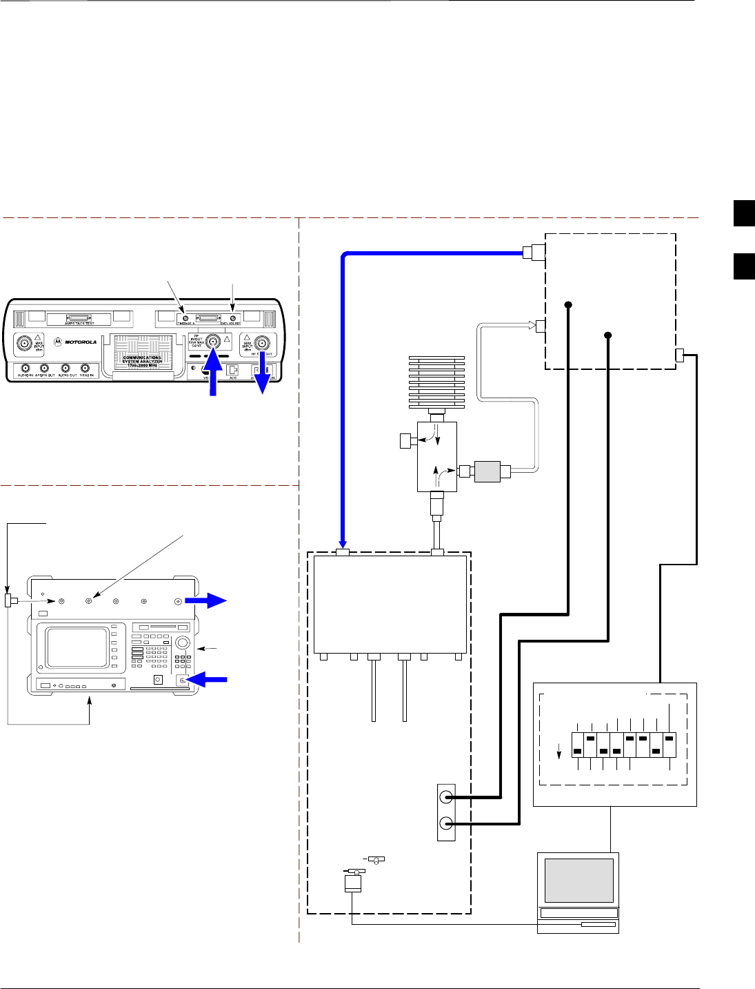
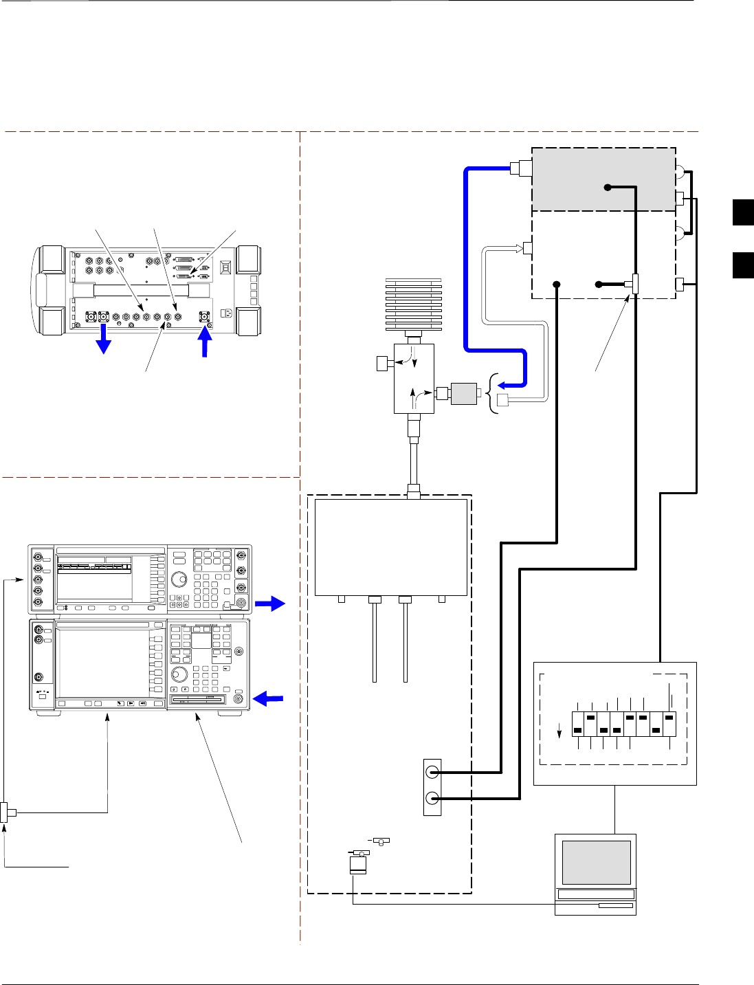
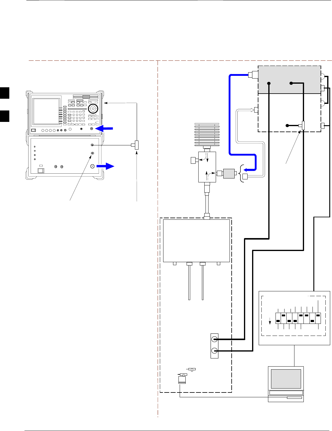
Set–up for Optimization/ATP Figure 3-14 and Figure 3-15 show the test set connections for
optimization/ATP tests.
Motorola CyberTest
TEST SETS Optimization/ATP SET UP
RF
IN/OUT
SYNC MONITOR
EVEN SEC TICK
PULSE REFERENCE
FROM CSM BOARD
FREQ MONITOR
19.6608 MHZ CLOCK
REFERENCE FROM
CSM BOARD
Advantest Model R3465
INPUT 50Ω
GPIB CONNECTS
TO BACK OF UNIT
NOTE: The 30 dB directional coupler is not
used with the Cybertest test set. The TX
cable is connected directly to the Cybertest
test set.
RF OUT 50Ω
FREQ MONITOR
19.6608 MHZ CLOCK
REFERENCE FROM
CSM BOARD
RF GEN
OUT
SYNC MONITOR EVEN
SEC TICK PULSE
REFERENCE FROM
CSM BOARD
BNC
“T”
TO EXT TRIGGER CONNECTOR
ON REAR OF TEST SET
(FOR DETAILS, SEE FIGURE F-3)
Figure 3-14: IS–95A/B Optimization/ATP Test Set–up, TRDC Shown – CyberTest and Advantest R3465
TO
MPC
TO LPA
TRUNKING
MODULE
RS232–GPIB
INTERFACE BOX
INTERNAL PCMCIA
ETHERNET CARD
GPIB
CABLE
UNIVERSAL TWISTED PAIR (UTP)
CABLE (RJ45 CONNECTORS)
RS232 NULL
MODEM
CABLE
S MODE
DATA FORMAT
BAUD RATE
GPIB ADRS G MODE
ON
BTS
INTERNAL
TX
CABLE
CDMA
LMF
DIP SWITCH SETTINGS
10BASET/
10BASE2
CONVERTER
LAN
B
LAN
A
RX TEST
CABLE
GPIB
RF IN/OUT
OR
INPUT 50 Ω
RF GEN OUT
OR RF OUT 50Ω
RX
ANTENNA
CONNECTOR
FREQ
MONITOR
SYNC
MONITOR
CSM
INTERNAL
RX
CABLE
TX
ANT
CPLD
RX
BTS
CPLD
TRDC
TX
BTS
CPLD
RX
ANT
CPLD
TX
ANTENNA
CONNECTOR
COMMUNICATIONS
SYSTEM ANALYZER
50 Ω
TERM
.
TX TEST
CABLE
DIRECTIONAL
COUPLER
(30 DB)
100–WATT (MIN.)
NON–RADIATING
RF LOAD
TX TEST
CABLE
* BLACK RECTANGLES
REPRESENT THE RAISED
PART OF SWITCHES
CDMA
TIMEBASE
IN
EVEN
SECOND/
SYNC IN
NOTE: IF BTS IS EQUIPPED
WITH DRDCS (DUPLEXED
RX/TX SIGNALS), BOTH THE
TX AND RX TEST CABLES
CONNECT TO THE DRDC
ANTENNA CONNECTOR.
(SEE FIGURE 3-16.)
2O DB IN–LINE
ATTENUATOR
3
Test Equipment Set–up – continued
SCt4812ET BTS Optimization/ATP — CDMA LMF Jan 2002
3-66
RF OUT
ONLY
Hewlett Packard Model HP 8921A W/PCS Interface
(for 1900 MHz)
GPIB
CONNECTS
TO BACK OF
UNITS
SYNC MONITOR
EVEN SEC TICK
PULSE REFERENCE
FROM CSM BOARD
FREQ MONITOR
19.6608 MHZ CLOCK
REFERENCE FROM
CSM BOARD
TEST SETS Optimization/ATP SET UP
RF
IN/OUT
GPIB
CONNECTS
TO BACK OF
UNIT
SYNC MONITOR
EVEN SEC TICK
PULSE REFERENCE
FROM CSM BOARD
FREQ MONITOR
19.6608 MHZ CLOCK
REFERENCE FROM
CSM BOARD
Hewlett Packard Model HP 8921A
(for 800 MHz)
RF
IN/OUT
DUPLEX
OUT
Figure 3-15: IS–95A/B Optimization/ATP Test Setup – HP 8921A
TO
MPC
TO LPA
TRUNKING
MODULE
RS232–GPIB
INTERFACE BOX
INTERNAL PCMCIA
ETHERNET CARD
GPIB
CABLE
UNIVERSAL TWISTED PAIR (UTP)
CABLE (RJ45 CONNECTORS)
RS232 NULL
MODEM
CABLE
S MODE
DATA FORMAT
BAUD RATE
GPIB ADRS G MODE
ON
BTS
INTERNAL
TX
CABLE
CDMA
LMF
DIP SWITCH SETTINGS
10BASET/
10BASE2
CONVERTER
LAN
B
LAN
A
RX TEST
CABLE
GPIB
PCS INTERFACE
INPUT/OUTPUT
PORTS
RX
ANTENNA
CONNECTOR
FREQ
MONITOR
SYNC
MONITOR
CSM
INTERNAL
RX
CABLE
TX
ANT
CPLD
RX
BTS
CPLD
TRDC
TX
BTS
CPLD
RX
ANT
CPLD
TX
ANTENNA
CONNECTOR
COMMUNICATIONS
SYSTEM ANALYZER
50 Ω
TERM
.
TX TEST
CABLE
DIRECTIONAL
COUPLER
(30 DB)
100–WATT (MIN.)
NON–RADIATING
RF LOAD
TX TEST
CABLE
* BLACK RECTANGLES
REPRESENT THE RAISED
PART OF SWITCHES
CDMA
TIMEBASE
IN EVEN
SECOND/
SYNC IN
NOTE: IF BTS IS EQUIPPED
WITH DRDCS (DUPLEXED
RX/TX SIGNALS), BOTH THE
TX AND RX TEST CABLES
CONNECT TO THE DRDC
ANTENNA CONNECTOR.
(SEE FIGURE 3-16.)
HP PCS
INTERFACE*
2O DB IN–LINE
ATTENUATOR
* FOR 1900 MHZ
ONLY
RF OUT ONLY
RF IN/OUT
NOTE:
FOR 800 MHZ TESTING, CONNECT CABLES TO THE
HP 8921A AS FOLLOWS:
RX TEST CABLE TO DUPLEX OUT
TX TEST CABLE TO RF IN/OUT
3
Test Equipment Set–up – continued
Jan 2002 3-67
SCt4812ET BTS Optimization/ATP — CDMA LMF
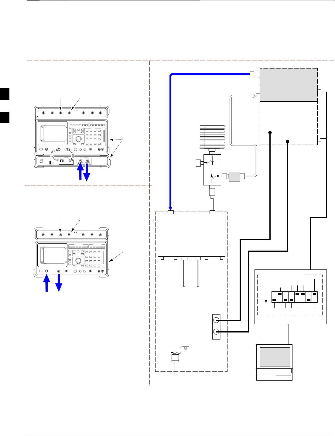
Agilent 8935 Series E6380A (formerly HP 8935)
DUPLEX OUT
TEST SETS Optimization/ATP SET UP
RF IN/OUT
HP–IB
TO GPIB
BOX
SYNC MONITOR
EVEN SEC TICK
PULSE REFERENCE
FROM CSM BOARD
FREQ MONITOR
19.6608 MHZ CLOCK
REFERENCE FROM
CSM BOARD
Figure 3-16: IS–95A/B and CDMA2000 1X Optimization/ATP Test Setup With DRDCs –
Agilent Test Equipment
RF INPUT
50 Ω
RF
OUTPUT
50 Ω
Agilent E4432B (Top) and E4406A (Bottom)
FREQ MONITOR
19.6608 MHZ CLOCK
REFERENCE FROM
CSM BOARD
SYNC MONITOR
EVEN SEC TICK
PULSE REFERENCE
FROM CSM BOARD
BNC
“T”
TO TRIGGER IN
ON REAR OF
TRANSMITTER
TESTER
TO PATTERN TRIG IN
ON REAR OF SIGNAL
GENERATOR
TO EXT REF IN
ON REAR OF
TRANSMITTER
TESTER
NOTE:
10 MHZ IN ON REAR OF SIGNAL GENERATOR IS CONNECTED TO
10 MHZ OUT (SWITCHED) ON REAR OF TRANSMITTER TESTER
(FIGURE F-5).
TO
MPC
TO LPA
TRUNKING
MODULE
RS232–GPIB
INTERFACE BOX
INTERNAL PCMCIA
ETHERNET CARD
GPIB
CABLE
UNIVERSAL TWISTED
PAIR (UTP) CABLE
(RJ45 CONNECTORS)
RS232 NULL
MODEM
CABLE
S MODE
DATA FORMAT
BAUD RATE
GPIB ADRS G MODE
ON
BTS
INTERNAL
TX
CABLE
CDMA
LMF
DIP SWITCH SETTINGS *
10BASET/
10BASE2
CONVERTER
LAN
B
LAN
A
COMMUNICATIONS
SYSTEM ANALYZER
GPIB
FREQ
MONITOR
SYNC
MONITOR
CSM
INTERNAL
RX
CABLE
DRDC
BTS
CPLD
ANT
CPLD
SIGNAL GENERATOR
GPIB
10 MHZ
IN
10 MHZ
OUT
TRIGGER IN
OR
EVEN SEC
SYNCH IN
EXT
REF
IN
BNC
“T”
PATTERN
TRIG IN
10 MHZ
REF OUT
* BLACK RECTANGLES
REPRESENT THE RAISED
PART OF SWITCHES
DUPLEXED
TX/RX
ANTENNA
CONNECTOR
RX TEST
CABLE
50 Ω
TERM
.
TX TEST
CABLE
DIRECTIONAL
COUPLER
(30 DB)
100–WATT (MIN.)
NON–RADIATING
RF LOAD
TX TEST
CABLE
2O DB IN–LINE
ATTENUATOR
NOTE:
THE AGILENT 8935 WITH OPTION 200 OR R2K CAN PERFORM 1X
TX ACCEPTANCE TESTING BUT NOT 1X RX ACCEPTANCE
TESTING. AN EXTERNAL SIGNAL GENERATOR MUST BE USED TO
PERFORM 1X RX TESTING.
RF IN/OUT
OR
RF INPUT
50 Ω
RF OUTPUT 50 Ω
OR DUPLEX OUT
3
Test Equipment Set–up – continued
SCt4812ET BTS Optimization/ATP — CDMA LMF Jan 2002
3-68
TEST SETS Optimization/ATP SET UP
Figure 3-17: IS–95A/B and CDMA2000 1X Optimization/ATP Test Setup With DRDCs –
Advantest R3267/3562 Test Equipment
INPUT 50 Ω
RF OUT
50 Ω
Advantest R3267 (Top) and R3562 (Bottom)
FREQ MONITOR
19.6608 MHZ CLOCK
REFERENCE FROM
CSM BOARD
SYNC MONITOR
EVEN SEC TICK
PULSE REFERENCE
FROM CSM BOARD
BNC
“T”
NOTE:
SYNTHE REF IN ON REAR OF SIGNAL GENERATOR IS
CONNECTED TO 10 MHZ REF OUT ON REAR OF
SPECTRUM ANALYZER
TO EXT TRIG
ON REAR OF
SPECTRUM
ANALYZER
TO
MPC
TO LPA
TRUNKING
MODULE
RS232–GPIB
INTERFACE BOX
INTERNAL PCMCIA
ETHERNET CARD
GPIB
CABLE
UNIVERSAL TWISTED
PAIR (UTP) CABLE
(RJ45 CONNECTORS)
RS232 NULL
MODEM
CABLE
S MODE
DATA FORMAT
BAUD RATE
GPIB ADRS G MODE
ON
BTS
INTERNAL
TX
CABLE
CDMA
LMF
DIP SWITCH SETTINGS
10BASET/
10BASE2
CONVERTER
LAN
B
LAN
A
INPUT
50 Ω
RF OUT
50 Ω
FREQ
MONITOR
SYNC
MONITOR
CSM
INTERNAL
RX
CABLE
DRDC
BTS
CPLD
ANT
CPLD
BNC
“T”
SPECTRUM
ANALYZER
GPIB
SIGNAL GENERATOR
GPIB
SYNTHE
REF
IN
10 MHZ
OUT
EXT
TRIG IN
MOD TIME
BASE IN
EXT TRIG
* BLACK RECTANGLES
REPRESENT THE RAISED
PART OF SWITCHES
DUPLEXED
TX/RX
ANTENNA
CONNECTOR
RX TEST
CABLE
50 Ω
TERM
.
TX TEST
CABLE
DIRECTIONAL
COUPLER
(30 DB)
100–WATT (MIN.)
NON–RADIATING
RF LOAD
TX TEST
CABLE
2O DB IN–LINE
ATTENUATOR
3
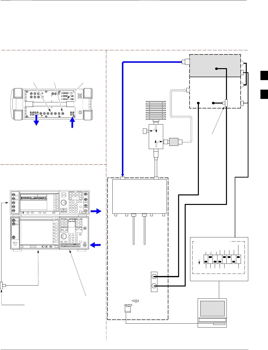
Test Equipment Set–up – continued
Jan 2002 3-69
SCt4812ET BTS Optimization/ATP — CDMA LMF
Agilent 8935 Model E6380A (formerly HP 8935)
DUPLEX OUT
TEST SETS Optimization/ATP SET UP
RF IN/OUT
HP–IB
TO GPIB
BOX
TO
MPC
TO LPA
TRUNKING
MODULE
RS232–GPIB
INTERFACE BOX
INTERNAL PCMCIA
ETHERNET CARD
GPIB
CABLE
UNIVERSAL TWISTED
PAIR (UTP) CABLE
(RJ45 CONNECTORS)
RS232 NULL
MODEM
CABLE
S MODE
DATA FORMAT
BAUD RATE
GPIB ADRS G MODE
ON
BTS
INTERNAL
TX
CABLE
CDMA
LMF
DIP SWITCH SETTINGS
10BASET/
10BASE2
CONVERTER
LAN
B
LAN
A
RX TEST
CABLE
COMMUNICATIONS
SYSTEM ANALYZER
GPIB
RF IN/OUT
OR RF INPUT 50 Ω
RF OUTPUT 50 Ω
OR DUPLEX OUT
RX
ANTENNA
CONNECTOR
FREQ
MONITOR
SYNC
MONITOR
CSM
SYNC MONITOR
EVEN SEC TICK
PULSE REFERENCE
FROM CSM BOARD
FREQ MONITOR
19.6608 MHZ CLOCK
REFERENCE FROM
CSM BOARD
INTERNAL
RX
CABLE
Figure 3-18: IS–95A/B and CDMA2000 1X Optimization/ATP Test Setup With TRDCs –
Agilent Test Equipment
TX
ANT
CPLD
RX
BTS
CPLD
TRDC
TX
BTS
CPLD
RX
ANT
CPLD
TX
ANTENNA
CONNECTOR
RF INPUT
50 Ω
RF
OUTPUT
50 Ω
Agilent E4432B (Top) and E4406A (Bottom)
FREQ MONITOR
19.6608 MHZ CLOCK
REFERENCE FROM
CSM BOARD
SYNC MONITOR
EVEN SEC TICK
PULSE REFERENCE
FROM CSM BOARD
BNC
“T”
TO TRIGGER IN
ON REAR OF
TRANSMITTER
TESTER
TO PATTERN TRIG IN
ON REAR OF SIGNAL
GENERATOR
TO EXT REF IN
ON REAR OF
TRANSMITTER
TESTER
NOTE:
10 MHZ IN ON REAR OF SIGNAL GENERATOR IS CONNECTED TO
10 MHZ OUT (SWITCHED) ON REAR OF TRANSMITTER TESTER
(FIGURE F-5).
SIGNAL GENERATOR
GPIB
10 MHZ
IN
10 MHZ
OUT
50 Ω
TERM
.
TX TEST
CABLE
DIRECTIONAL
COUPLER
(30 DB)
100–WATT (MIN.)
NON–RADIATING
RF LOAD
TRIGGER IN
OR
EVEN SEC
SYNCH IN
EXT
REF
IN
TX TEST
CABLE
BNC
“T”
PATTERN
TRIG IN
* BLACK RECTANGLES
REPRESENT THE RAISED
PART OF SWITCHES
2O DB IN–LINE
ATTENUATOR
NOTE:
THE AGILENT 8935 WITH OPTION 200 OR R2K CAN PERFORM 1X
TX ACCEPTANCE TESTING BUT NOT 1X RX ACCEPTANCE
TESTING. AN EXTERNAL SIGNAL GENERATOR MUST BE USED TO
PERFORM 1X RX TESTING.
3
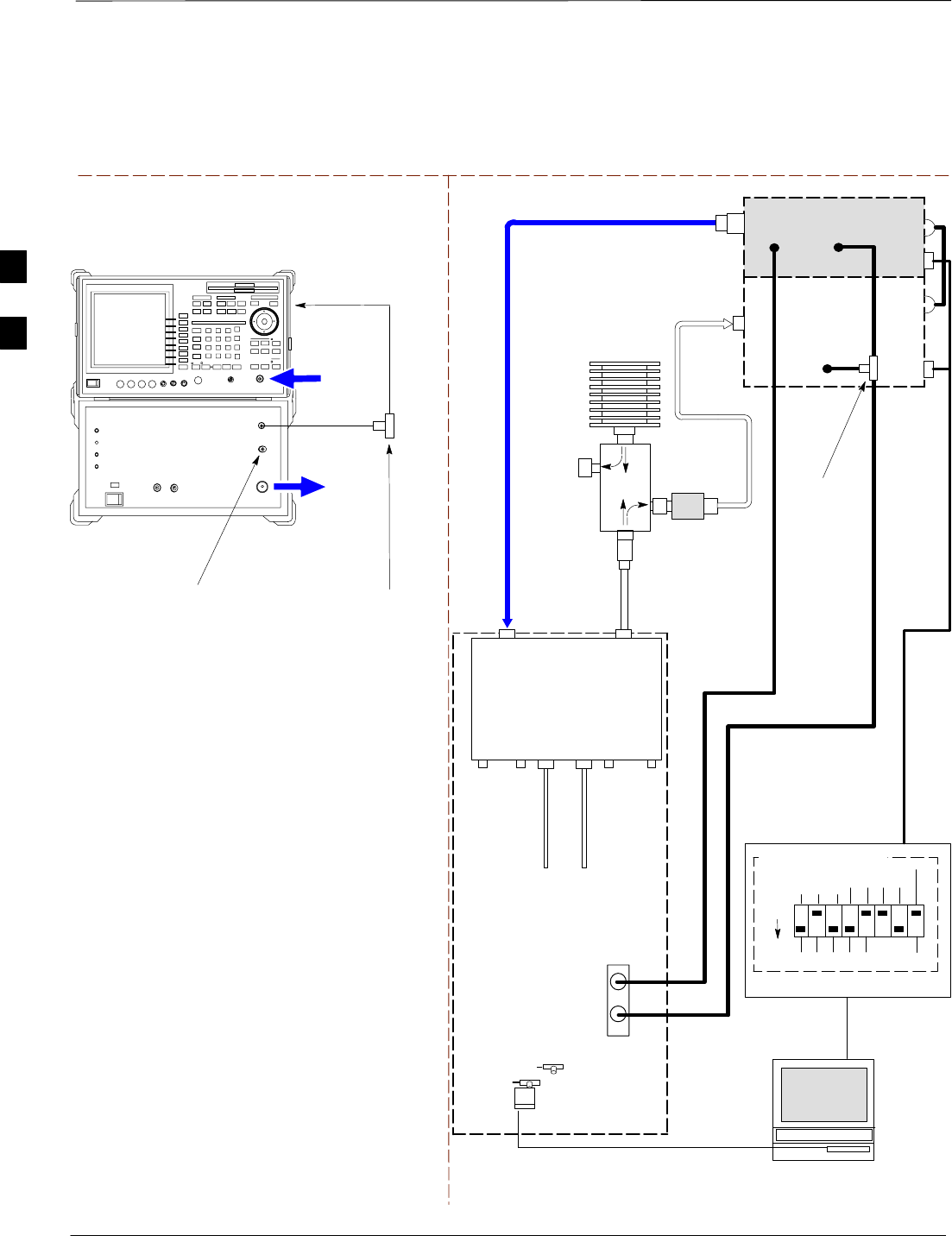
Test Equipment Set–up – continued
SCt4812ET BTS Optimization/ATP — CDMA LMF Jan 2002
3-70
TEST SETS Optimization/ATP SET UP
Figure 3-19: IS–95A/B and CDMA2000 1X Optimization/ATP Test Setup With TRDCs –
Advantest R3267/3562 Test Equipment
INPUT 50 Ω
RF OUT
50 Ω
Advantest R3267 (Top) and R3562 (Bottom)
FREQ MONITOR
19.6608 MHZ CLOCK
REFERENCE FROM
CSM BOARD
SYNC MONITOR
EVEN SEC TICK
PULSE REFERENCE
FROM CSM BOARD
BNC
“T”
NOTE:
SYNTHE REF IN ON REAR OF SIGNAL GENERATOR IS
CONNECTED TO 10 MHZ REF OUT ON REAR OF
SPECTRUM ANALYZER
TO EXT TRIG
ON REAR OF
SPECTRUM
ANALYZER
TO
MPC
TO LPA
TRUNKING
MODULE
RS232–GPIB
INTERFACE BOX
INTERNAL PCMCIA
ETHERNET CARD
GPIB
CABLE
UNIVERSAL TWISTED
PAIR (UTP) CABLE
(RJ45 CONNECTORS)
RS232 NULL
MODEM
CABLE
S MODE
DATA FORMAT
BAUD RATE
GPIB ADRS G MODE
ON
BTS
INTERNAL
TX
CABLE
CDMA
LMF
DIP SWITCH SETTINGS
10BASET/
10BASE2
CONVERTER
LAN
B
LAN
A
RX TEST
CABLE
SPECTRUM
ANALYZER
GPIB
INPUT
50 Ω
RF OUT
50 Ω
RX
ANTENNA
CONNECTOR
FREQ
MONITOR
SYNC
MONITOR
CSM
INTERNAL
RX
CABLE
TX
ANTENNA
CONNECTOR
SIGNAL GENERATOR
GPIB
SYNTHE
REF
IN
10 MHZ
OUT
50 Ω
TERM
.
TX TEST
CABLE
DIRECTIONAL
COUPLER
(30 DB)
100–WATT (MIN.)
NON–RADIATING
RF LOAD
EXT
TRIG IN
MOD TIME
BASE IN
TX TEST
CABLE
BNC
“T”
EXT TRIG
* BLACK RECTANGLES
REPRESENT THE RAISED
PART OF SWITCHES
TX
ANT
CPLD
RX
BTS
CPLD
TRDC
TX
BTS
CPLD
RX
ANT
CPLD
2O DB IN–LINE
ATTENUATOR
3
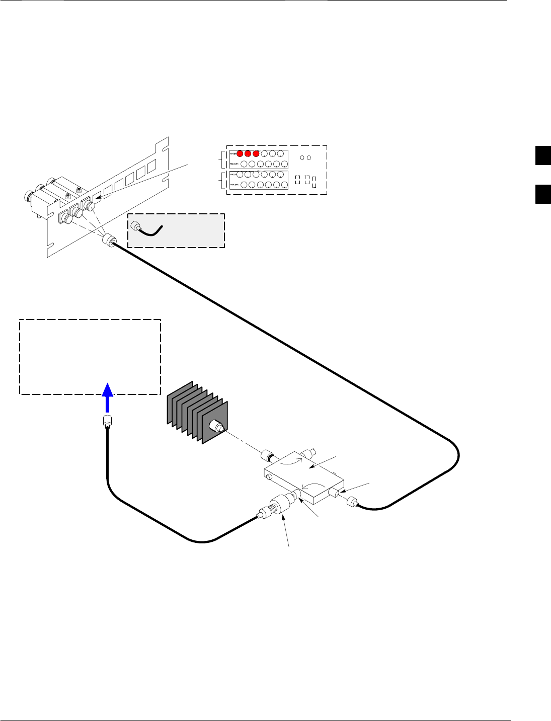
Test Equipment Set–up – continued
Jan 2002 3-71
SCt4812ET BTS Optimization/ATP — CDMA LMF
TX ATP Setup
Figure 3-20 shows a typical TX ATP setup.
Figure 3-20: Typical TX ATP Setup with Directional Coupler (shown with and without RFDS)
30 DB
DIRECTIONAL
COUPLER
40W NON–RADIATING
RF LOAD
OUTPUT
PORT
RVS (REFLECTED)
PORT 50–OHM
TERMINATION
FWD
(INCIDENT)
PORT
BTS INPUT
PORT TX TEST
CABLE
ONE 20 DB 20 W IN LINE
ATTENUATOR
Connect TX test cable between
the directional coupler input port
and the appropriate TX antenna
directional coupler connector.
TX ANTENNA DIRECTIONAL COUPLERS
RFDS RX (RFM TX) COUPLER
OUTPUTS TO RFDS FWD(BTS)
ASU2 (SHADED) CONNECTORS
RX
(RFM TX)
TX
(RFM RX)
COBRA RFDS Detail
1
23
RF FEED LINE TO
DIRECTIONAL
COUPLER
REMOVED
COMMUNICATIONS
TEST SET
IN
Appropriate test sets and the port
names for all model test sets are
described in Table 3-28.
TX
TEST
CABLE
TX RF FROM BTS FRAME
TEST
DIRECTIONAL
COUPLER
NOTE:
THIS SETUP APPLIES TO BOTH
STARTER AND EXPANSION FRAMES. FW00116
3
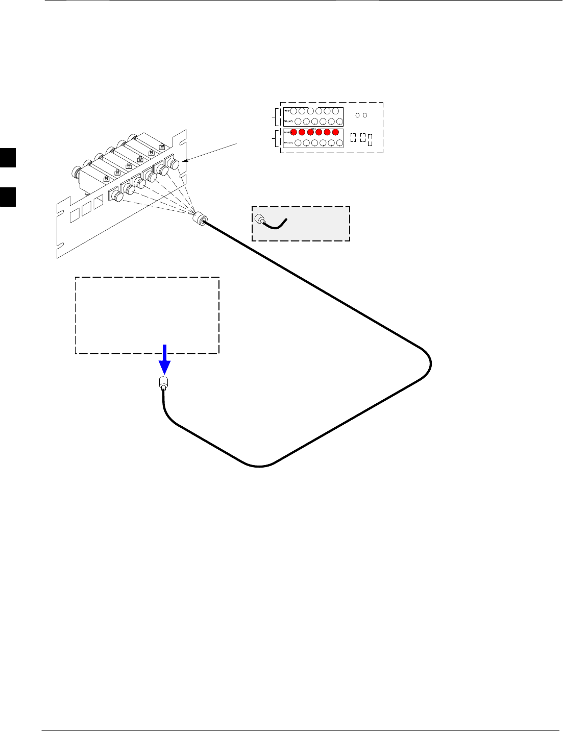
Test Equipment Set–up – continued
SCt4812ET BTS Optimization/ATP — CDMA LMF Jan 2002
3-72
Figure 3-21: Typical RX ATP Setup with Directional Coupler (shown with or without RFDS)
RX RF FROM BTS
FRAME
3
4
1
2
5
6
Connect RX test cable between
the test set and the appropriate
RX antenna directional coupler.
RX ANTENNA DIRECTIONAL COUPLERS
RF FEED LINE TO
TX ANTENNA
REMOVED
COMMUNICATIONS
TEST SET
RFDS TX (RFM RX) COUPLER
OUTPUTS TO RFDS FWD(BTS)
ASU1 (SHADED) CONNECTORS
RX
(RFM TX)
TX
(RFM RX)
COBRA RFDS Detail
OUT
Appropriate test sets and the port
names for all model test sets are
described in Table 3-28.
RX Test
Cable
NOTE:
THIS SETUP APPLIES TO BOTH
STARTER AND EXPANSION FRAMES.
FW00115
3
Test Set Calibration
Jan 2002 3-73
SCt4812ET BTS Optimization/ATP — CDMA LMF
Background
Proper test equipment setup ensures that the test equipment and
associated test cables do not introduce measurement errors, and that
measurements are correct.
If the test set being used to interface with the BTS has been
calibrated and maintained as a set, this procedure does not
need to be performed. (Test Set includes LMF terminal,
communications test set, additional test equipment,
associated test cables, and adapters.)
NOTE
This procedure must be performed prior to beginning the optimization.
Verify all test equipment (including all associated test cables and
adapters actually used to interface all test equipment and the BTS) has
been calibrated and maintained as a set.
If any piece of test equipment, test cable, or RF adapter,
that makes up the calibrated test equipment set, has been
replaced, re-calibration must be performed. Failure to do so
can introduce measurement errors, resulting in incorrect
measurements and degradation to system performance.
CAUTION
Calibration of the communications test set (or equivalent
test equipment) must be performed at the site before
calibrating the overall test set. Calibrate the test equipment
after it has been allowed to warm–up and stabilize for a
minimum of 60 minutes.
IMPORTANT
*
Purpose
These procedures access the CDMA LMF automated calibration routine
used to determine the path losses of the supported communications
analyzer, power meter, associated test cables, and (if used) antenna
switch that make up the overall calibrated test set. After calibration, the
gain/loss offset values are stored in a test measurement offset file on the
CDMA LMF.
3

Test Set Calibration – continued
SCt4812ET BTS Optimization/ATP — CDMA LMF Jan 2002
3-74
GPIB Addresses
GPIB addresses can range from 1 through 30. The LMF will accept any
address in that range, but the numbers entered in the LMF Options
window GPIB address box must match the addresses of the test
equipment. Motorola recommends using 1 for a CDMA signal generator,
13 for a power meter, and 18 for a communications system analyzer. To
verify and, if necessary, change the GPIB addresses of the test
equipment, refer to the Setting GPIB Addresses section of Appendix F.
Selecting Test Equipment
Use LMF Options from the Options menu list to select test equipment
automatically (using the autodetect feature) or manually.
Prerequisites
A Serial Connection and a Network Connection tab are provided for
test equipment selection. The Serial Connection tab is used when the
test equipment items are connected directly to the CDMA LMF
computer via a GPIB box (normal setup). The Network Connection tab
is used when the test equipment is to be connected remotely via a
network connection.
Ensure the following has been completed before selecting test
equipment:
STest equipment is correctly connected and turned on.
SCDMA LMF computer serial port and test equipment are connected to
the GPIB box.
Manually Selecting Test
Equipment in a Serial
Connection Tab
Test equipment can be manually specified before, or after, the test
equipment is connected. CDMA LMF does not check to see if the test
equipment is actually detected for manual specification.
Table 3-30: Selecting Test Equipment Manually in a Serial Connection Tab
Step Action
1From the Tools menu, select Options.
The LMF Options window appears.
2Click on the Serial Connection tab (if not in the forefront).
3Select the correct serial port in the COMM Port pick list (normally COM1).
4Click on the Manual Specification button (if not enabled).
5Click on the check box corresponding to the test item(s) to be used.
3
Test Set Calibration – continued
Jan 2002 3-75
SCt4812ET BTS Optimization/ATP — CDMA LMF
Table 3-30: Selecting Test Equipment Manually in a Serial Connection Tab
Step Action
6Type the GPIB address in the corresponding GPIB address box (refer to the Setting GPIB Addresses
section of Appendix F for directions on verifying and/or changing test equipment GPIB addresses).
Motorola–recommended addresses are:
1 = signal generator
13 = power meter
18 = communications system analyzer
* IMPORTANT
When test equipment items are manually selected by the operator, the LMF defaults to using a power
meter for RF power measurements. The LMF will use a communications system analyzer for RF
power measurements only if a power meter is not selected (power meter checkbox not checked).
7Click on Apply. (The button will darken until the selection has been committed.)
8Click on Dismiss to close the test equipment window.
3

Test Set Calibration – continued
SCt4812ET BTS Optimization/ATP — CDMA LMF Jan 2002
3-76
Automatically Selecting Test
Equipment in a Serial
Connection Tab When using the auto-detection feature to select test equipment, the
CDMA LMF examines which test equipment items are actually
communicating with CDMA LMF. Follow the procedure in Table 3-31
to use the auto-detect feature.
Table 3-31: Selecting Test Equipment Using Auto-Detect
Step Action
1From the Tools menu, select Options.
The LMF Options window appears.
2Click on the Serial Connection tab (if not in the forefront).
3Select the correct serial port in the COMM Port pick list (normally COM1).
4Click on Auto–Detection (if not enabled).
5Type in the GPIB addresses in the box labeled GPIB address to search (if not already displayed).
NOTE
Refer to the Setting GPIB addresses section of Appendix F for instructions on verifying or changing
test equipment GPIB addresses, if necessary.
When both a power meter and analyzer are selected, the first item listed in the GPIB addresses to
search box will be used for RF power measurements (i.e., TX calibration). The address for a signal
generator is normally 1, a power meter is normally 13 and the address for a CDMA analyzer is
normally 18. If 1, 13,18 are included in the GPIB addresses to search box, the power meter (13) will
be used for RF power measurements. If the test equipment items are manually selected the CDMA
analyzer is used only if a power meter is not selected.
6 Click Apply. The button will darken until the selection has been committed. A check mark will
appear in the Manual Configuration section for detected test equipment items.
7 Click Dismiss to close the LMF Options window.
3

Test Set Calibration – continued
Jan 2002 3-77
SCt4812ET BTS Optimization/ATP — CDMA LMF
Calibrating Test Equipment
The calibrate test equipment function zeros the power measurement level
of the test equipment item that is to be used for TX calibration and audit.
If both a power meter and an analyzer are connected, only the power
meter is zeroed.
Calibrate Test Equipment from the Util menu list is used to calibrate
test equipment item before being used for testing. The test equipment
must be selected before beginning calibration. Follow the procedure in
Table 3-32 to calibrate the test equipment.
Table 3-32: Test Equipment Calibration
Step Action
1From the Util menu, select Calibrate Test Equipment. A Directions window is displayed. Follow
the instructions provided.
2Follow the direction provided.
3Click on Continue to close the Directions window. A status window is displayed.
4Click on OK to close the status report window.
Calibrating Cables
The cable calibration function is used to measure the loss (in dB) for the
TX and RX cables that are to be used for testing. A CDMA analyzer is
used to measure the loss of each cable configuration (TX cable
configuration and RX cable configuration). The cable calibration
consists of the following procedures.
SMeasure the loss of a short cable. This is done to compensate for any
measurement error of the analyzer. The short cable, which is used only
for the calibration process, is used in series with both the TX and RX
cable configuration when they are measured. The measured loss of the
short cable is deducted from the measured loss of the TX and RX
cable configuration to determine the actual loss of the TX and RX
cable configurations. This deduction is done so any error in the
analyzer measurement will be adjusted out of both the TX and RX
measurements.
SMeasure the short cable plus the RX cable configuration loss is
measured. The RX cable configuration normally consists only of a
coax cable with type–N connectors that is long enough to reach from
the BTS RX port the test equipment.
SMeasure the short cable plus the TX cable configuration loss is
measured. The TX cable configuration normally consists of two coax
cables with type–N connectors and a directional coupler, a load, and
an additional attenuator if required by the BTS type. The total loss of
the path loss of the TX cable configuration must be as required for the
BTS (normally 30 or 50 dB). The Motorola Cybertest analyzer is
different in that the required attenuation/load is built into the test set
so the TX cable configuration consists only of the required length
coax cable.
3

Test Set Calibration – continued
SCt4812ET BTS Optimization/ATP — CDMA LMF Jan 2002
3-78
Calibrating Cables with a
CDMA Analyzer
The Cable Calibration menu item from the Util menu list is used to
calibrate both TX and RX test cables for use with CDMA LMF.
LMF cable calibration cannot be accomplished with an
HP8921A analyzer for 1.9 MHz. A different analyzer type
or the signal generator and spectrum analyzer method must
be used (refer to Table 3-34 and Table 3-35). Cable
calibration values must be manually entered if the signal
generator and spectrum analyzer method is used. For the
HP8921A, refer to Appendix F.
NOTE
The test equipment must be selected before this procedure can be started.
Follow the procedure in Table 3-33 to calibrate the cables.
Table 3-33: Cable Calibration
Step Action
1From the Util menu, select Cable Calibration. A Cable Calibration window is displayed.
2Enter a channel number(s) in the Channels box. Multiple channels numbers must be separated with a
comma, no space (i.e., 200,800). When two or more channels numbers are entered, the cables will be
calibrated for each channel. Interpolation will be accomplished for other channels as required for TX
calibration.
3 Select TX and RX CABLE CAL, TX CABLE CAL or RX CABLE CAL in the Cable Calibration
picklist.
4 Click OK. Follow the directions displayed for each step. A status report window will be displayed
with the results of the cable calibration.
3
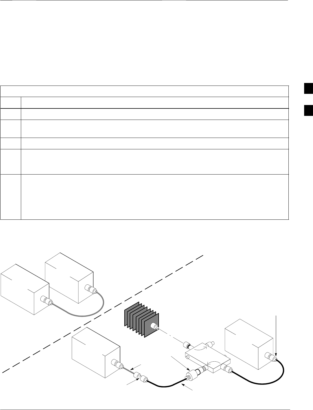
Test Set Calibration – continued
Jan 2002 3-79
SCt4812ET BTS Optimization/ATP — CDMA LMF
Calibrating TX Cables Using a
Signal Generator and
Spectrum Analyzer
Follow the procedure in Table 3-34 to calibrate the TX cables using the
signal generator and spectrum analyzer. Refer to Figure 3-22 for a
diagram of the signal generator and spectrum analyzer.
Table 3-34: Calibrating TX Cables Using Signal Generator and Spectrum Analyzer
Step Action
1Connect a short test cable between the spectrum analyzer and the signal generator.
2Set signal generator to 0 dBm at the customer frequency of 869–894 MHz for 800 MHz CDMA and
1930–1990 MHz band for North American PCS.
3Use spectrum analyzer to measure signal generator output (see Figure 3-22, “A”) and record the value.
4Connect the spectrum analyzer’s short cable to point “B”, as shown in the lower portion of the
diagram, to measure cable output at customer frequency (869–894 MHz for 800 MHz CDMA and
1930–1990 MHz for North American PCS) and record the value at point “B”.
5Calibration factor = A – B Example: Cal = –1 dBm – (–53.5 dBm) = 52.5 dB
NOTE
The short cable is used for calibration only. It is not part of the final test setup. After calibration is
completed, do not re-arrange any cables. Use the equipment setup, as is, to ensure test procedures use
the correct calibration factor.
Figure 3-22: Calibrating Test Equipment Setup for TX Cable Calibration
(Using Signal Generator and Spectrum Analyzer)
50 OHM
TERMINATION
30 DB
DIRECTIONAL
COUPLER
Spectrum
Analyzer
Signal
Generator
A
Spectrum
Analyzer
40W NON–RADIATING
RF LOAD
B
SHORT TEST CABLE
Signal
Generator
THIS WILL BE THE CONNECTION TO THE
POWER METER DURING TX CALIBRATION
AND TO THE CDMA ANALYZER DURING TX
ATP TESTS.
SHORT
TEST
CABLE THIS WILL BE THE CONNECTION
TO THE TX PORTS DURING TX
CALIBRATION AND TO THE TX/RX
PORTS DURING ATP TESTS.
SECOND RF
TEST CABLE.
ONE 20DB 20 W IN
LINE ATTENUATOR
FW00293
3
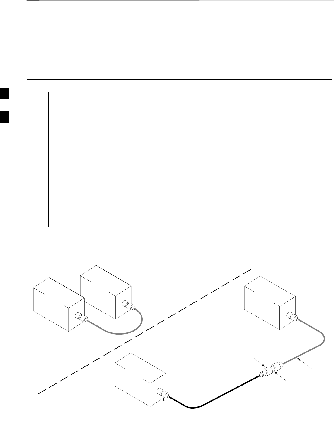
Test Set Calibration – continued
SCt4812ET BTS Optimization/ATP — CDMA LMF Jan 2002
3-80
Calibrating RX Cables Using a
Signal Generator and
Spectrum Analyzer Follow the procedure in Table 3-35 to calibrate the RX cables using the
signal generator and spectrum analyzer. Refer to Figure 3-23, if required.
Table 3-35: Calibrating RX Cables Using a Signal Generator and Spectrum Analyzer
Step Action
1Connect a short test cable to the spectrum analyzer and connect the other end to the Signal Generator.
2Set signal generator to –10 dBm at the customer’s RX frequency of 824–840 MHz for 800 MHz
CDMA and 1850–1910 MHz band for North American PCS.
3Use spectrum analyzer to measure signal generator output (see Figure 3-23, “A”) and record the value
for “A”.
4Connect the test setup, as shown in the lower portion of the diagram, to measure the output at the
customer’s RX frequency in the 1850–1910 MHz band. Record the value at point ‘‘B”.
5Calibration factor = A – B
Example: Cal = –12 dBm – (–14 dBm) = 2 dB
NOTE
The short test cable is used for test equipment setup calibration only. It is not be part of the final test
setup. After calibration is completed, do not re-arrange any cables. Use the equipment setup, as is, to
ensure test procedures use the correct calibration factor.
Figure 3-23: Calibrating Test Equipment Setup for RX ATP Test
(Using Signal Generator and Spectrum Analyzer)
Spectrum
Analyzer
Signal
Generator
A
B
Spectrum
Analyzer
SHORT
TEST
CABLE
SHORT TEST
CABLE
CONNECTION TO THE OUTPUT
PORT DURING RX MEASUREMENTS
Signal
Generator
BULLET
CONNECTOR
LONG
CABLE 2
CONNECTION TO THE RX PORTS
DURING RX MEASUREMENTS. FW00294
3

Test Set Calibration – continued
Jan 2002 3-81
SCt4812ET BTS Optimization/ATP — CDMA LMF
Setting Cable Loss Values Cable loss values for the TX and RX test cable configurations are
normally set by accomplishing cable calibration with use of the
applicable test equipment. The resulting values are stored in the cable
loss files. The cable loss values can also be set/changed manually.
Prerequisites
SLogged into the BTS
Table 3-36: Setting Cable Loss Values
Step Action
1Click on the Util menu.
2 Select Edit >Cable Loss > TX or RX. A data entry pop–up window will appear.
3Click on the Add Row button to add a new channel number. Then click in the Channel # and Loss
(dBm) columns and enter the desired values.
4To edit existing values click in the data box to be changed and change the value.
5To delete a row, click on the row and then click on the Delete Row button.
6Click on the Save button to save displayed values.
7Click on the Dismiss button to exit the window. Values that were entered/changed after the Save
button was used will not be saved.
NOTE
SIf cable loss values exist for two different channels the LMF will interpolate for all other channels.
SEntered values will be used by the LMF as soon as they are saved. You do not have to logout and
login.
3

Test Set Calibration – continued
SCt4812ET BTS Optimization/ATP — CDMA LMF Jan 2002
3-82
Setting Coupler Loss Value If an in–service coupler is installed the coupler loss (e.g., 30 dB) must be
manually entered so it will be included in the LMF TX calibration and
audit calculations and the RX FER test.
Prerequisites
SLogged into the BTS
Table 3-37: Setting Coupler Loss Values
Step Action
1Click on the Util menu.
2 Select Edit >Coupler Loss>TX or RX. A data entry pop–up window will appear.
3Click in the Loss (dBm) column for each carrier that has a coupler and enter the appropriate value.
4To edit existing values click in the data box to be changed and change the value.
5Click on the Save button to save displayed values.
6Click on the Dismiss button to exit the window. Values that were entered/changed after the Save
button was used will not be saved.
NOTE
SThe In–Service Calibration check box in the Tools>Options>BTS Options tab must checked
before entered coupler loss values will be used by the TX calibration and audit functions or RX Fer
test.
SEntered values will be used by the LMF as soon as they are saved. You do not have to logout and
login.
3

Bay Level Offset Calibration
Jan 2002 3-83
SCt4812ET BTS Optimization/ATP — CDMA LMF
Introduction
Calibration compensates for normal equipment variations within the
BTS and assures maximum measurement accuracy.
RF Path Bay Level Offset
Calibration
Calibration identifies the accumulated gain in every transmit path (BBX
slot) at the BTS site and stores that value in the CAL file. The BLOs are
subsequently downloaded to each BBX.
Each receive path starts at a BTS RX antenna port and terminates at a
backplane BBX slot. Each transmit path starts at a BBX backplane slot,
travels through the LPA, and terminates at a BTS TX antenna port.
Calibration identifies the accumulated gain in every transmit path (BBX
slot) at the BTS site and stores that value in the CAL file. Each transmit
path starts at a C–CCP shelf backplane BBX slot, travels through the
LPA, and ends at a BTS TX antenna port. When the TX path calibration
is performed, the RX path BLO will automatically be set to the default
value.
When to Calibrate BLOs Calibration of BLOs is required after initial BTS installation.
The BLO data of an operational BTS site must be re-calibrated once
each year. Motorola recommends re-calibrating the BLO data for all
associated RF paths after replacing any of the following components or
associated interconnecting RF cabling:
SBBX board
SC–CCP shelf
SCIO card
SCIO to LPA backplane RF cable
SLPA backplane
SLPA
STX filter / TX filter combiner
STX thru-port cable to the top of frame
3
Bay Level Offset Calibration – continued
SCt4812ET BTS Optimization/ATP — CDMA LMF Jan 2002
3-84
TX Path Calibration
The TX Path Calibration assures correct site installation, cabling, and the
first order functionality of all installed equipment. The proper function
of each RF path is verified during calibration. The external test
equipment is used to validate/calibrate the TX paths of the BTS.
Before installing any test equipment directly to any TX
OUT connector you must first verify that there are no
CDMA channels keyed. Have the OMC–R place the sector
assigned to the LPA under test OOS. Failure to do so can
result in serious personal injury and/or equipment damage.
WARNING
Always wear a conductive, high impedance wrist strap
while handling any circuit card/module. If this is not done,
there is a high probability that the card/module could be
damaged by ESD.
CAUTION
At new site installations, to facilitate the complete test of
each CCP shelf (if the shelf is not already fully populated
with BBX boards), move BBX boards from shelves
currently not under test and install them into the empty
BBX slots of the shelf currently being tested to insure that
all BBX TX paths are tested.
–This procedure can be bypassed on operational sites
that are due for periodic optimization.
–Prior to testing, view the CDF file to verify the
correct BBX slots are equipped. Edit the file as
required to include BBX slots not currently equipped
(per Systems Engineering documentation).
IMPORTANT
*
3
Bay Level Offset Calibration – continued
Jan 2002 3-85
SCt4812ET BTS Optimization/ATP — CDMA LMF
BLO Calibration Data File
During the calibration process, the LMF creates a calibration (BLO) data
file. After calibration has been completed, this offset data must be
downloaded to the BBXs using the Download BLO function. An
explanation of the file is shown below.
Due to the size of the file, Motorola recommends that you
print out a hard copy of a bts.cal file and refer to it for the
following descriptions.
NOTE
The CAL file is subdivided into sections organized on a per slot basis (a
slot Block).
Slot 1 contains the calibration data for the 12 BBX slots. Slot 20
contains the calibration data for the redundant BBX (see Table 3-39).
Each BBX slot header block contains:
SA creation Date and Time – broken down into separate parameters of
createMonth, createDay, createYear, createHour, and createMin.
SThe number of calibration entries – fixed at 720 entries corresponding
to 360 calibration points of the CAL file including the slot header and
actual calibration data.
SThe calibration data for a BBX is organized as a large flat array. The
array is organized by branch, BBX slot, and calibration point.
–The first breakdown of the array indicates which branch the
contained calibration points are for. The array covers transmit, main
receive and diversity receive offsets as follows:
Table 3-38: BLO BTS.cal file Array Branch Assignments
Range Assignment
C[1]–C[240] Transmit
C[241]–C[480] Receive
C[481]–C[720] Diversity Receive
3

Bay Level Offset Calibration – continued
SCt4812ET BTS Optimization/ATP — CDMA LMF Jan 2002
3-86
–The second breakdown of the array is per sector. Three sectors are
allowed.
Table 3-39: BTS.cal File Array (Per Sector)
BBX Sectorization TX RX RX Diversity
Slot[1] (Primary BBXs 1 through 12)
1 (Omni) 3–Sector, C[1]–C[20] C[241]–C[260] C[481]–C[500]
23–Sector,
1st C[21]–C[40] C[261]–C[280] C[501]–C[520]
36 Sector, Carrier C[41]–C[60] C[281]–C[300] C[521]–C[540]
41st
Carrier 3–Sector, C[61]–C[80] C[301]–C[320] C[541]–C[560]
5Carrier 3–Sector,
3rd C[81]–C[100] C[321]–C[340] C[561]–C[580]
6Carrier C[101]–C[120] C[341]–C[360] C[581]–C[600]
73–Sector, C[121]–C[140] C[361]–C[380] C[601]–C[620]
83–Sector,
2nd C[141]–C[160] C[381]–C[400] C[621]–C[640]
96 Sector, Carrier C[161]–C[180] C[401]–C[420] C[641]–C[660]
10 2nd
Carrier 3–Sector, C[181]–C[200] C[421]–C[440] C[661]–C[680]
11 Carrier 3–Sector,
4th C[201]–C[220] C[441]–C[460] C[681]–C[700]
12 Carrier C[221]–C[240] C[461]–C[480] C[701]–C[720]
Slot[20] (Redundant BBX–13)
1 (Omni) 3–Sector, C[1]–C[20] C[241]–C[260] C[481]–C[500]
23–Sector,
1st C[21]–C[40] C[261]–C[280] C[501]–C[520]
36 Sector, Carrier C[41]–C[60] C[281]–C[300] C[521]–C[540]
41st
Carrier 3–Sector, C[61]–C[80] C[301]–C[320] C[541]–C[560]
5Carrier 3–Sector,
3rd C[81]–C[100] C[321]–C[340] C[561]–C[580]
6Carrier C[101]–C[120] C[341]–C[360] C[581]–C[600]
73–Sector, C[121]–C[140] C[361]–C[380] C[601]–C[620]
83–Sector,
2nd C[141]–C[160] C[381]–C[400] C[621]–C[640]
96 Sector, Carrier C[161]–C[180] C[401]–C[420] C[641]–C[660]
10 2nd
Carrier 3–Sector, C[181]–C[200] C[421]–C[440] C[661]–C[680]
11 Carrier 3–Sector,
4th C[201]–C[220] C[441]–C[460] C[681]–C[700]
12 Carrier C[221]–C[240] C[461]–C[480] C[701]–C[720]
SRefer to the hard copy of the file. As you can see, 10 calibration
points per sector are supported for each branch. Two entries are
required for each calibration point.
SThe first value (all odd entries) refer to the CDMA channel
(frequency) the BLO is measured at. The second value (all even
entries) is the power set level. The valid range for PwrLvlAdj is from
2500 to 27500 (2500 corresponds to –125 dBm and 27500
corresponds to +125 dBm).
3

Bay Level Offset Calibration – continued
Jan 2002 3-87
SCt4812ET BTS Optimization/ATP — CDMA LMF
SThe 20 calibration entries for each slot/branch combination must be
stored in order of increasing frequency. If less than 10 points
(frequencies) are calibrated, the largest frequency that is calibrated is
repeated to fill out the 10 points.
Example:
C[1]=384, odd cal entry = 1 ‘‘calibration point”
C[2]=19102, even cal entry
C[3]=777,
C[4]=19086,
.
.
C[19]=777,
C[20]=19086, (since only two cal points were calibrated this
would be repeated for the next 8 points)
SWhen the BBX is loaded with BLO data, the cal file data for the BBX
is downloaded to the device in the order it is stored in the CAL file.
TxCal data is sent first, C[1] – C[60]. BBX slot 1’s 10 calibration
points are sent (C[1] – C[20]), followed by BBX slot 2’s 10
calibration points (C[21] – C[40]), etc. The RxCal data is sent next,
followed by the RxDCal data.
STemperature compensation data is also stored in the cal file for each
slot.
Test Equipment Setup:
RF Path Calibration
Follow the steps in Table 3-40 to set up test equipment.
Table 3-40: Test Equipment Setup (RF Path Calibration)
Step Action
NOTE
Verify the GPIB is properly connected and turned on.
! CAUTION
To prevent damage to the test equipment, all transmit (TX) test connections must be via the 30 dB
directional coupler for 800 MHz or via a 30 dB coupler with a 20 dB in–line attenuator for 1900 MHz.
1Connect the LMF computer terminal to the BTS LAN A connector on the BTS (if you have not
already done so). Refer to the procedure in Table 3-6.
SIf required, calibrate the test equipment per the procedure in Table 3-32.
SConnect the test equipment as shown in Figure 3-17, Figure 3-18 and Figure 3-19.
3

Bay Level Offset Calibration – continued
SCt4812ET BTS Optimization/ATP — CDMA LMF Jan 2002
3-88
Transmit (TX) Path Calibration
The assigned channel frequency and power level (as measured at the top
of the frame) for transmit calibration is derived from the site CDF file.
For each BBX, the channel frequency is specified in the ChannelList
CDF file parameter and the power is specified in the SIFPilotPwr
CDF file parameter for the sector associated with the BBX (located
under the ParentSECTOR field of the ParentCARRIER CDF file
parameter).
The calibration procedure attempts to adjust the power to within +0.5 dB
of the desired power. The calibration will pass if the error is less than
+1.5 dB.
The TX Bay Level Offset at sites WITHOUT the directional coupler
option, is approximately 42.0 dB ±3.0 dB.
SAt sites WITHOUT RFDS option, BLO is approximately
42.0 dB ±4.0 dB. A typical example would be TX output power
measured at BTS (36.0 dBm) minus the BBX TX output level
(approximately –6.0 dBm) would equate to 42 dB BLO.
The TX Bay Level Offset at sites WITH the directional coupler option,
is approximately 41.4 dB ±3.0 dB. TX BLO = Frame Power Output
minus BBX output level.
SExample: TX output power measured at RFDS TX coupler
(39.4 dBm) minus the BBX TX output level (approximately
–2.0 dBm) and RFDS directional coupler/cable (approximately
–0.6 dBm) would equate to 41.4 dB BLO.
The LMF Tests menu list items, TX Calibration and All Cal/Audit,
perform the TX BLO Calibration test for a XCVR(s). The All Cal/Audit
menu item performs TX calibration, downloads BLO, and performs TX
audit if the TX calibration passes. All measurements are made through
the appropriate TX output connector using the calibrated TX cable setup.
Test Pattern Drop–down Pick List
Pilot is shown as the default setting in this pick list box. The full range
of available selections and their descriptions are as follows:
Standard – performs calibration or audit using pilot, paging, synch, and
six traffic channels with IS–97–specified gain. This pattern setting
should be used for all non–in–service calibrations and audits. Using this
pattern setting requires the selection of both a BBX and at least one
MCC.
Pilot (default) – performs calibration using only the pilot channel. This
pattern setting should be used for in–service calibrations, and requires
selection of only a BBX.
CDFPilot –This pattern setting is for advanced users. It performs
calibration or audit using the CDF value for pilot gain and IS–97 gain
values for all the other channels included in the Standard pattern setting
(paging, synch, and six traffic). Using this pattern setting requires the
selection of both a BBX and at least one MCC.
3

Bay Level Offset Calibration – continued
Jan 2002 3-89
SCt4812ET BTS Optimization/ATP — CDMA LMF
CDF – This pattern setting is for advanced users who need to use CDF
gain settings for all channels included in the Standard pattern setting
(pilot, paging, synch, and six traffic). Using this pattern setting requires
the selection of both a BBX and at least one MCC.
Verify BLO
In both the TX Calibration and All Cal/Audit dialog boxes, a Verify
BLO checkbox is provided and checked by default. After the actual TX
calibration is completed during either the TX Calibration or All
Cal/Audit process, the BLO derived from the calibration is compared to
a standard, acceptable BLO tolerance for the BTS. In some installations,
additional items may be installed in the transmit path. The additional
change in gain from these items could cause BLO verification failure
and, therefore, failure of the entire calibration. In these cases, either the
Verify BLO checkbox should be unchecked or the additional path losses
should be added into each applicable sector using the
Util>Edit>TX Coupler Loss function.
Single–Sided BLO
Normally valid values are some value plus–or–minus some offset. If
single–sided BLO” is selected, the result will only be considered a
success if it’s in the lower half of the range. If it was normally success
from 37–47 (which is 42± 5), single–sided BLO” would make it a
success only if the result was from 37–42.
Prerequisites
Before running this test, ensure that the following have been done:
SCSM–1, GLIs, MCCs, and BBXs have correct code load and data
load.
SPrimary CSM and MGLI are INS.
SAll BBXs are OOS_RAM.
STest equipment and test cables are calibrated and connected for TX
BLO calibration.
SLMF is logged into the BTS.
Connect the test equipment as shown in Figure 3-11 and Figure 3-12 and
follow the procedure in Table 3-41 to perform the TX calibration test.
Before installing any test equipment directly to any TX
OUT connector, first verify there are no CDMA BBX
channels keyed. Failure to do so can result in serious
personal injury and/or equipment damage.
WARNING
3
Bay Level Offset Calibration – continued
SCt4812ET BTS Optimization/ATP — CDMA LMF Jan 2002
3-90
Verify all BBX boards removed and repositioned have been
returned to their assigned shelves/slots. Any BBX boards
moved since they were downloaded will have to be
downloaded again.
IMPORTANT
*
Table 3-41: BTS TX Path Calibration
nStep Action
1Select the BBX(s) to be calibrated.
NOTE
If STANDARD, CDF or CDFPILOT is selected for TEST PATTERN, then at least one MCC
must be also selected.
2From the Tests menu, select TX>TX Calibration.
3Select the appropriate carrier(s) displayed in the Channels/Carrier pick list. (Press and hold the
<Shift> or <Ctrl> key to select multiple items.)
4Type the appropriate channel number in the Carrier n Channels box.
5 Select Verify BLO (default) or Single–sided BLO.
NOTE
Single–sided BLO is only used when checking non–redundant transceivers.
6From the Test Pattern pick list, select a test pattern.
NOTE
SSelecting PILOT (default) performs tests using a pilot signal only.
SSelecting STANDARD performs tests using pilot, synch, paging and six traffic channels. This
requires an MCC to be selected.
SSelecting CDFPilot performs tests using the CDF value for pilot gain and IS–97 gain values for
all the other channels included in the Standard pattern setting (paging, synch, and six traffic).
Using this pattern setting requires the selection of both a BBX and at least one MCC.
SSelecting CDF performs tests using pilot, synch, paging and six traffic channels, however, the
gain for the channel elements is specified in the CDF file.
7Click on OK.
8Follow the cable connection directions as they are displayed.
A status report window displays the test results.
9Click on Save Results or Dismiss to close the status report window.
3
Bay Level Offset Calibration – continued
Jan 2002 3-91
SCt4812ET BTS Optimization/ATP — CDMA LMF
Exception Handling
In the event of a failure, the calibration procedure displays a FAIL
message in the status report window and provides information in the
Description field.
Recheck the test setup and connection and re–run the test. If the tests fail
again, note specifics about the failure, and refer to Chapter 6,
Troubleshooting.
Download BLO Procedure
After a successful TX path calibration, download the BLO calibration
file data to the BBXs. BLO data is extracted from the CAL file for the
BTS and downloaded to the selected BBX devices.
If a successful All Cal/Audit was completed, this
procedure does not need to be performed, as BLO is
downloaded as part of the All Cal/Audit.
NOTE
Prerequisites
Ensure the following prerequisites have been met before proceeding.
SBBXs being downloaded are OOS–RAM (yellow).
STX calibration is successfully completed.
Follow the steps in Table 3-42 to download the BLO data to the BBXs.
Table 3-42: Download BLO
Step Action
1Select the BBX(s) to be downloaded.
2From the Device menu, select Download>BLO.
A status report window displays the result of the download.
NOTE
Selected device(s) do not change color when BLO is downloaded.
3 Click OK to close the status report window.
3
Bay Level Offset Calibration – continued
SCt4812ET BTS Optimization/ATP — CDMA LMF Jan 2002
3-92
Calibration Audit Introduction
The BLO calibration audit procedure confirms the successful generation
and storage of the BLO calibrations. The calibration audit procedure
measures the path gain or loss of every BBX transmit path at the site. In
this test, actual system tolerances are used to determine the success or
failure of a test. The same external test equipment set up is used.
*RF path verification, BLO calibration, and BLO data
download to BBXs must have been successfully completed
prior to performing the calibration audit.
IMPORTANT
Transmit (TX) Path Audit
Perform the calibration audit of the TX paths of all equipped BBX slots,
per the steps in Table 3-43.
Before installing any test equipment directly to any TX
OUT connector, first verify there are no CDMA BBX
channels keyed. Failure to do so can result in serious
personal injury and/or equipment damage.
WARNING
If a successful All Cal/Audit was completed, this
procedure does not need to be performed, as BLO is
downloaded as part of the All Cal/Audit.
NOTE
3

Bay Level Offset Calibration – continued
Jan 2002 3-93
SCt4812ET BTS Optimization/ATP — CDMA LMF
TX Audit Test
The Tests menu item, TX Audit, performs the TX BLO Audit test for a
BBX(s). All measurements are made through the appropriate TX output
connector using the calibrated TX cable setup.
Prerequisites
Before running this test, the following should be done:
SCSM–1,GLI2s, BBXs have correct code load.
SPrimary CSM and MGLI2 are INS.
SAll BBXs are OOS_RAM.
STest equipment and test cables are calibrated and connected for TX
BLO calibration.
SLMF is logged into the BTS.
Follow the procedure in Table 3-43 to perform the BTS TX Path Audit
test.
3

Bay Level Offset Calibration – continued
SCt4812ET BTS Optimization/ATP — CDMA LMF Jan 2002
3-94
Table 3-43: BTS TX Path Audit
nStep Action
1Select the BBX(s) to be audited.
NOTE
If STANDARD or CDF is selected for Test Pattern, then at least one MCC must be also selected.
2From the Tests menu, select TX>TX Audit.
3Select the appropriate carrier(s) displayed in the Channels/Carrier pick list.
Press and hold the <Shift> or <Ctrl> key to select multiple items.
4Type the appropriate channel number in the Carrier n Channels box.
5 Select Verify BLO (default) or Single–sided BLO.
NOTE
Single–sided BLO is only used when checking non–redundant transceivers.
6From the Test Pattern pick list, select a test pattern.
NOTE
SSelecting PILOT (default) performs tests using a pilot signal only.
SSelecting STANDARD performs tests using pilot, synch, paging and six traffic channels. This
requires an MCC to be selected.
SSelecting CDFPILOT performs tests using the CDF value for pilot gain and IS–97 gain values
for all the other channels included in the Standard pattern setting (paging, synch, and six
traffic). Using this pattern setting requires the selection of both a BBX and at least one MCC.
SSelecting CDF performs tests using pilot, synch, paging and six traffic channels, however, the
gain for the channel elements is specified in the CDF file.
7Click on OK.
8Follow the cable connection directions as they are displayed.
A status report window displays the test results.
9Click on Save Results or Dismiss to close the status report window.
Exception Handling
In the event of a failure, the calibration procedure displays a FAIL
message in the status report window and provides information in the
Description field.
Recheck the test setup and connection and re–run the test. If the tests fail
again, note specifics about the failure, and refer to Chapter 6,
Troubleshooting.
3
Bay Level Offset Calibration – continued
Jan 2002 3-95
SCt4812ET BTS Optimization/ATP — CDMA LMF
All Cal/Audit Test
The Tests menu item, All Cal/Audit, performs the TX BLO Calibration
and Audit test for a XCVR(s). All measurements are made through the
appropriate TX output connector using the calibrated TX cable setup.
If the TX calibration portion of the test passed, the BLO
data will automatically be downloaded to the BBX(s)
before the audit portion of the test is run.
NOTE
Prerequisites
Before running this test, the following should be done:
SCSM–1, GLI2s, BBXs have correct code and data load.
SPrimary CSM and MGLI2 are INS.
SAll BBXs are OOS_RAM.
STest equipment and test cables are calibrated and connected for TX
BLO calibration.
SLMF is logged into the BTS.
Follow the procedures in Table 3-44 to perform the All Cal/Audit test.
Before installing any test equipment directly to any TX
OUT connector, first verify there are no CDMA BBX
channels keyed. Failure to do so can result in serious
personal injury and/or equipment damage.
WARNING
3

Bay Level Offset Calibration – continued
SCt4812ET BTS Optimization/ATP — CDMA LMF Jan 2002
3-96
Table 3-44: All Cal/Audit Test
nStep Action
1Select the BBX(s) to be tested.
NOTE
If STANDARD, CDF or CDFPILOT is selected for TEST PATTERN, then at least one MCC
must be also selected.
2From the Tests menu, select All Cal/Audit.
3Select the appropriate carrier(s) displayed in the Channels/Carrier pick list.
Press and hold the <Shift> or <Ctrl> key to select multiple items.
4Type the appropriate channel number in the Carrier n Channels box.
5 Select Verify BLO or Single–sided BLO.
NOTE
Single–sided BLO is only used when checking non–redundant transceivers.
6From the Test Pattern pick list, select a test pattern.
NOTE
SSelecting Pilot (default) performs tests using a pilot signal only.
SSelecting Standard performs tests using pilot, synch, paging and 6 traffic channels. This
requires an MCC to be selected.
SSelecting CDFPilot performs tests using the CDF value for pilot gain and IS–97 gain values for
all the other channels included in the Standard pattern setting (paging, synch, and six traffic).
Using this pattern setting requires the selection of both a BBX and at least one MCC.
SSelecting CDF performs tests using pilot, synch, paging and 6 traffic channels, however, the
gain for the channel elements is specified in the CDF file.
7Click on OK.
8Follow the cable connection directions as they are displayed.
A status report window displays the test results.
9Click on Save Results or Dismiss to close the status report window.
3
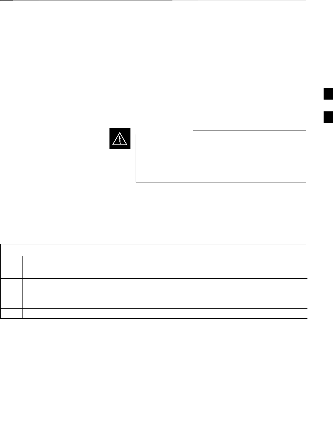
Bay Level Offset Calibration – continued
Jan 2002 3-97
SCt4812ET BTS Optimization/ATP — CDMA LMF
Create CAL File
The Create Cal File function gets the BLO data from BBXs and
creates/updates the CAL file for the BTS. If a CAL file does not exist a
new one is created. If a CAL file already exists it is updated. After a
BTS has been fully optimized a copy of the CAL file must exist so it can
be transferred to the CBSC. If TX calibration has been successfully
performed for all BBXs and BLO data has been downloaded, a CAL file
will exist. Note the following:
SThe Create Cal File function only applies to selected (highlighted)
BBXs.
Editing the CAL file is not encouraged as this action can
cause interface problems between the BTS and the LMF.
To manually edit the CAL file you must first logout of the
BTS. If you manually edit the CAL file and then use the
Create Cal File function the edited information will be lost.
WARNING
Prerequisites
Before running this test, the following should be done:
SLMF is logged in to the BTS
SBBXs are OOS_RAM with BLO downloaded
Table 3-45: Create CAL File
Step Action
1Select the applicable BBXs. The CAL file will only be updated for the selected BBXs.
2Click on the Device menu.
3Click on the Create Cal File menu item.
The status report window is displays the results of the action.
4 Click OK.
3

RFDS Setup and Calibration
SCt4812ET BTS Optimization/ATP — CDMA LMF Jan 2002
3-98
RFDS Description
The optional RFDS is used to perform RF tests of the site from the
CBSC or from the LMF. The RFDS contains the following FRUs:
SAntenna Select Unit (ASU)
SFixed Wireless Terminal Interface Card (FWTIC)
SSubscriber Unit Assembly (SUA)
For complete information regarding the RFDS, refer to the CDMA
CDMA RFDS Hardware Installation; 68P64113A93, CDMA RFDS
User’s Guide; 68P64114A51, and the LMF Help function on–line
documentation.
RFDS Parameters
The bts–#.cdf file includes RFDS parameter settings that must match the
installed RFDS equipment. The paragraphs below describe the editable
parameters and their defaults. Table 3-46 explains how to edit the
parameter settings.
SRfdsEquip – valid inputs are 0 through 2.
0 = (default) RFDS is not equipped
1 = Non-Cobra/Patzer box RFDS
2 = Cobra RFDS
STsuEquip – valid inputs are 0 or 1
0 = (default) TSU not equipped
1 = TSU is equipped in the system
SMC1....4 – valid inputs are 0 or 1
0 = (default) Not equipped
1 = Multicouplers equipped in RFDS system
(SC9600 internal RFDS only)
SAsu1/2Equip – valid inputs are 0 or 1
0 = (default) Not equipped
1 = Equipped
STestOrigDN – valid inputs are ’’’ (default) or a numerical string up to
15 characters. (This is the phone number the RFDS dials when
originating a call. A dummy number needs to be set up by the switch,
and is to be used in this field.)
Any text editor may be used to open the bts–#.cdf file to
verify, view, or modify data. Because the bts–#.cdf file is
generated on a Unix system, a more sophisticated editor,
such as MicroSoft WordPad, will display file content in a
more easily–read format than many simple text editors.
NOTE
Checking and Setting RFDS
Parameters
Follow the procedure in Table 3-46 to review and/or edit RFDS
parameters.
3

RFDS Setup and Calibration – continued
Jan 2002 3-99
SCt4812ET BTS Optimization/ATP — CDMA LMF
Table 3-46: RFDS Parameter Settings
Step Action
1* IMPORTANT
Log out of the BTS prior to perform this procedure.
Using a text editor, verify the following fields are set correctly in the bts–#.cdf file:
EXAMPLE:
Asu1Equip = 1
Asu2Equip = 0 (1 if system is non-duplexed)
Mc1Equip = 0
Mc2Equip = 0
Mc3Equip = 0
Mc4Equip = 0
RfdsEquip = 2
TestOrigDN = ’123456789’
TsuEquip = 1
NOTE
The above is an example of entries extracted from the bts–#.cdf file that should have been generated
by the OMC–R and copied to the LMF. These fields will have been set by the OMC–R if the
RFDSPARM database is modified for the RFDS.
2Save changes and/or quit the editor.
3Log into the BTS using an LMF GUI session(refer to Table 3-14).
4 If no changes were made to the bts–#.cdf file fields listed in step 1, proceed to Step 7. If changes were
made, continue with Step 5.
5* IMPORTANT
To make certain the complete data download is accepted, the MGLI should be OOS_RAM (yellow)
when RFDS parameter settings are downloaded.
When changes are made to RFDS parameters in the bts–#.cdf file, data must be downloaded to the
MGLI by performing the following:
5a –To be sure it does not take control when the MGLI is disabled, manually disable the redundant
GLI card by unseating it from the backplane connectors and sliding it partially out of the shelf
slot.
5b –Click on the MGLI.
5c –Click on Device in the BTS menu bar, and select Disable from the pull–down menu.
–– A status report window is displayed showing status of the operation.
5d –When the operation is complete, click OK to close the status report window.
5e –Click on the MGLI (now OOS_RAM (yellow)).
5f –Click on Device in the BTS menu bar, and select Download > Data from the pull–down menus
(selected devices do not change color when data is downloaded).
–– A status report window is displayed showing status of the download.
. . . continued on next page
3

RFDS Setup and Calibration – continued
SCt4812ET BTS Optimization/ATP — CDMA LMF Jan 2002
3-100
Table 3-46: RFDS Parameter Settings
Step Action
5g –Click OK to close the status report window.
5h –Click on the MGLI.
5i –Click on Device in the BTS menu bar, and select Enable from the pull–down menu.
–– A status report window is displayed showing status of the operation.
5j –When the operation is complete, click OK to close the status report window.
! CAUTION
When the MGLI changes to INS_ACT, data will automatically be downloaded to the RFDS. During
this process, the RFDS LED will slowly begin flashing red and green for approximately 2–3 minutes.
DO NOT attempt to perform any functions with the RFDS until the LED remains steady green.
5k –Re–seat the redundant GLI card into the backplane connectors and lock it in place with the ejector
tabs.
5l –Once the redundant GLI initializes, download data to it by selecting the card and, in the BTS
menu bar, clicking Device and selecting Download > Data from the pull–down menus.
6Any MCCs which were INS_ACT when the MGLI was disabled must be disabled, re–enabled, and
downloaded with code as follows:
6a –Select the devices to be reset by clicking on them or using Select from the BTS menu bar and
clicking on MCCs in the pull–down menu.
6b –In the BTS menu bar, click on Device and select Disable from the pull–down menu.
–– A status window report window is displayed showing status of the operation.
6c –Click OK to close the status report window.
6d –Download data to the MCCs by following the procedure in Table 3-21.
6e –When data download is complete, enable the MCCs by following the procedure in Table 3-24.
7Click on the RFDS tab.
8Status the RFDS TSU by performing the following:
8a –Click on the SUA to select it.
8b –Click on TSU in the BTS menu bar, and select Status TSU from the pull–down menu.
–– A status report is displayed showing the software version number for the TSIC and SUA.
. . . continued on next page
3
RFDS Setup and Calibration – continued
Jan 2002 3-101
SCt4812ET BTS Optimization/ATP — CDMA LMF
Table 3-46: RFDS Parameter Settings
Step Action
8c –Click OK to close the status report window.
* IMPORTANT
If the LMF displays an error message, check the following:
SEnsure AMR cable is correctly connected from the BTS to the RFDS.
SVerify RFDS has power.
SVerify RFDS status LED is green.
SVerify entries in RFDS fields of the bts–#.cdf file are correct (refer to step 1).
SStatus the MGLI and ensure it is communicating (by Ethernet) with the LMF, and is in the proper
state (INS_ACT (bright green)).
RFDS TSU NAM Programming
The Number Assignment Module (NAM) information needs to be
programmed into the TSU before it can receive and process test calls, or
be used for any type of RFDS test. The RFDS TSU NAM must be
programmed with the appropriate system parameters and phone number
during hardware installation. The TSU phone and TSU MSI must be
recorded for each BTS used for OMC–R RFDS software configuration.
The user will only need to program the NAM for the initial
installation of the RFDS.
NOTE
Explanation of Parameters
Used When Programming the
TSU NAM
Table 3-47 defines the parameters used when editing the tsu.nam file.
Table 3-47: Definition of Parameters
Access Overload Code
Slot Index
System ID
Network ID
These parameters are obtained from the switch.
Primary Channel A
Primary Channel B
Secondary Channel A
Secondary Channel B
These parameters are the channels which are to be used in operation
of the system.
Lock Code
Security Code
Service Level
Station Class Mark
Do NOT change.
3
RFDS Setup and Calibration – continued
SCt4812ET BTS Optimization/ATP — CDMA LMF Jan 2002
3-102
Table 3-47: Definition of Parameters
IMSI MCC
IMSI 11 12 These fields are obtained at the OMC using the following command:
OMC000>disp bts–# imsi
If the fields are blank, replace the IMSI fields in the NAM file to 0,
otherwise use the values displayed by the OMC.
MIN Phone Number These fields are the phone number assigned to the mobile. The ESN
and MIN must be entered into the switch as well.
NOTE
This field is different from the TODN field in the bts–#.cdf file. The
MIN is the phone number of the RFDS subscriber, and the TODN is
the number the subscriber calls.
Valid NAM Ranges Table 3-48 provides the valid NAM field ranges. If any of the fields are
missing or out-of–range, the RFDS will error out.
Table 3-48: Valid NAM Field Ranges
Valid Range
NAM Field Name Minimum Maximum
Access Overload Code 0 15
Slot Index 0 7
System ID 0 32767
Network ID 0 32767
Primary Channel A 25 1175
Primary Channel B 25 1175
Secondary Channel A 25 1175
Secondary Channel B 25 1175
Lock Code 0 999
Security Code 0 999999
Service Level N/A N/A
Station Class Mark 0 255
IMSI 11 12 0 99
IMSI MCC 0 999
MIN Phone Number N/A N/A
3

RFDS Setup and Calibration – continued
Jan 2002 3-103
SCt4812ET BTS Optimization/ATP — CDMA LMF
Set Antenna Map Data
The antenna map data must be entered manually if an RFDS is installed.
Antenna map data does not need to be entered if an RFDS is not
installed. The antenna map data is only used for RFDS tests and is
required if an RFDS is installed.
Prerequisite
SLMF is logged into the BTS
Follow the procedure in Table 3-49 to set antenna map data for the
RFDS.
Table 3-49: Set Antenna Map Data
Step Action
1Click on Util in the BTS menu bar, and select Edit > Antenna Map... from the pull–down menus.
–A tabbed data entry pop–up window will appear.
2In the data entry pop–up window, click on the TX Antenna Map or RX Antenna Map tab to select
the antenna map to be edited.
3Locate the carrier and sector number for which data is to be entered or edited, and click in the column
where entry or editing is needed.
4Enter/edit Antenna # and Antenna Label column data as needed for each carrier.
NOTE
Refer to the CDMA Help > Utility Menu > Edit–Antenna Map... section of LMF Help function
on–line documentation for antenna map examples.
5For each tab with changes, click on the Save button to save displayed values.
6Click on the Dismiss button to close the window.
NOTE
SValues entered or changed after the Save button was used will be lost when the window is
dismissed.
SEntered values will be used by the LMF as soon as they are saved. It is not necessary to log out and
log back into the LMF for changes to take effect.
3
RFDS Setup and Calibration – continued
SCt4812ET BTS Optimization/ATP — CDMA LMF Jan 2002
3-104
Set RFDS Configuration Data
If an RFDS is installed, the RFDS configuration data must be manually
entered.
Prerequisite
SLMF is logged into the BTS
The entered antenna# index numbers must correspond to
the antenna# index numbers used in the antenna maps.
IMPORTANT
*
Follow the procedure in Table 3-50 to set RFDS configuration data.
Table 3-50: Set RFDS Configuration Data
Step Action
1Click on Util in the BTS menu bar, and select Edit > RFDS Configuration... from the pull–down
menus.
–A tabbed data entry pop–up window will appear.
2In the data entry pop–up window, click on the TX RFDS Configuration or RX RFDS Configuration
tab, as required.
3To add a new antenna number, perform the following:
3a –Click on the Add Row button.
3b –Click in the Antenna #, Cal Antenna, Scap Antenna, or Populate [Y/N] columns, as required.
3c –Enter the desired data.
4To edit existing values click in the data box to be changed and change the value.
NOTE
Refer to the CDMA Help > Utility Menu > Edit–RFDS Configuration... section of LMF Help
function on–line documentation for RFDS configuration data examples.
5To delete a row, click on the row and then click on the Delete Row button.
6For each tab with changes, click on the Save button to save displayed values.
7Click on the Dismiss button to close the window.
NOTE
SValues entered or changed after the Save button was used will be lost when the window is
dismissed.
SEntered values will be used by the LMF as soon as they are saved. It is not necessary to log out and
log back into the LMF for changes to take effect.
3
RFDS Setup and Calibration – continued
Jan 2002 3-105
SCt4812ET BTS Optimization/ATP — CDMA LMF
RFDS Calibration
The RFDS Calibration option is used to calibrate the RFDS TX and RX
paths.
TX Path Calibration – For a TX antenna path calibration the BTS
XCVR is keyed at a pre–determined power level and the BTS power
output level is measured by the RFDS. The power level is then measured
at the TX antenna directional coupler by the power measuring test
equipment item being used (power meter or analyzer). The difference
(offset) between the power level at the RFDS and the power level at the
TX antenna directional coupler is used as the TX RFDS calibration
offset value.
RX Path Calibration – For an RX antenna path calibration the RFDS is
keyed at a pre–determined power level and the power input level is
measured by the BTS BBX. A CDMA signal at the same power level
measured by the BTS BBX is then injected at the RX antenna directional
coupler by the communications system analyzer. The difference (offset)
between the RFDS–keyed power level and power level measured at the
BTS BBX is the RFDS RX calibration offset value.
RFDS calibration and the CAL file – The TX and RX RFDS
calibration offset values are written to the CAL file in the slot[385]
Block.
TSIC channel frequency – For each RFDS TSIC, the channel
frequency is determined at the lower third and upper third of the
appropriate band using the frequencies listed in Table 3-51.
Table 3-51: RFDS TSIC Calibration Channel Frequencies
System Channel Calibration Points
800 MHz (A and B) 341 and 682
1.9 GHz 408 and 791
Before installing any test equipment directly to any TX
OUT connector, verify that there are no CDMA channels
keyed. Failure to do so can result in serious personal injury
and/or equipment damage.
WARNING
RFDS Calibration Procedure
Prerequisites
STest equipment has been selected.
STest equipment and test cables have been calibrated.
STX calibration has been performed and BLO data has been
downloaded to the BBXs.
3

RFDS Setup and Calibration – continued
SCt4812ET BTS Optimization/ATP — CDMA LMF Jan 2002
3-106
STest equipment and test cables are connected for TX calibration.
SAntenna map data has been entered for the site.
SBBXs are INS_TEST.
Follow the procedure in Table 3-52 to perform RFDS calibration.
Table 3-52: RFDS Calibration
Step Action
1In the LMF, select the FRAME tab.
2If it is not selected (no black dot showing), click on the B button in the BTS menu bar to select it.
3Select the BBX(s) assigned to the carrier(s) and sector(s) which will be used in RFDS calibration
(refer to Table 1-5 for BBX carrier and sector assignments).
4Click on RFDS in the BTS menu bar, and select RFDS Calibration... from the pull–down menu.
–An RFDS Calibration set–up window will be displayed.
5In the Tests to Perform box, select TX Calibration or RX Calibration, as required
6Enter the appropriate channel number(s) (refer to Table 3-51) in the Channel Field box.
STo enter more than one channel number, use the following methods:
–Separate non–sequential channel numbers with a comma and no spaces;
for example: 247,585,742.
–Enter a range of sequential channels by typing the first and last channel numbers in the range
separated by a dash and no spaces;
for example: 385–395.
7If the frame is equipped with TX combiners, click in the Has Combiners checkbox.
8Select the appropriate carrier(s) and sector(s) from the Carriers pick list (hold down the Shift or Ctrl
key while clicking on pick list items to select multiple carrier(s)–sector(s)).
9Select the appropriate RX branch (Both, Main, or Diversity) in the drop–down list.
10 In the Rate Set box, select the appropriate transfer rate (1=9600, 2=14400) from the drop–down list.
11 Click on the OK button.
–A status report window is displayed, followed by a Directions pop–up window.
12 Follow the cable connection directions as they are displayed.
13 When the test is completed, test results are displayed in the status report window.
14 Click on the OK button to close the status report window.
15 Click on the Frame tab.
16 Select the MGLI by clicking on it.
17 Download the CAL file, now updated with the RFDS offset data, to the MGLI by clicking on Device
on the BTS menu bar, and selecting Download > Data from the pull–down menus.
NOTE
The MGLI will automatically transfer the RFDS offset data from the CAL file to the RFDS.
3

RFDS Setup and Calibration – continued
Jan 2002 3-107
SCt4812ET BTS Optimization/ATP — CDMA LMF
Program TSU NAM
The NAM must be programmed before it can receive and process test
calls, or be used for any type of RFDS test.
Prerequisites
SMGLI is INS_ACT (bright green).
SSUA is powered up and has a code load.
Follow the procedure in Table 3-53 to program the TSU NAM.
Table 3-53: Program NAM Procedure
Step Action
1In the LMF, select the RFDS tab.
2Select the SUA by clicking on it.
3Click on TSU in the BTS menu bar, and select Program TSU NAM from the pull–down menu.
–A NAM programming window will appear.
4Enter the appropriate information in the boxes (see Table 3-47 and Table 3-48) .
5Click on the OK button to display the status report.
6Click on the OK button to close the status report window.
3

Alarms Testing
SCt4812ET BTS Optimization/ATP — CDMA LMF Jan 2002
3-108
Alarm Verification
The alarms testing should be performed at a convenient point in the
optimization/ATP process, since the LMF is necessary to ensure that the
RF cabinet is receiving the appropriate alarms from the power cabinet.
The SC 4812ET is capable of concurrently monitoring 10 customer
defined input signals and four customer defined outputs, which interface
to the 50–pin punchblock. All alarms are defaulted to “Not Equipped”
during ATP testing. Testing of these inputs is achieved by triggering the
alarms and monitoring the LMF for state–transition messages from the
active MGLI2.
All customer alarms are routed through the 50 pair punchblock located
in the I/O compartment at the back of the frame. Testing is best
accomplished by using a specialized connector that interfaces to the
50–pair punchblock. This connector is wired so that customer return 1 (2
for the B side) is connected to every input, CDI 0 through CDI 17.
Alarm Reporting Display
The Alarm Monitor window can be displayed to list alarms that occur
after the window is displayed. To access the Alarm Monitor window,
select Util>Alarm Monitor.
The following buttons are included:
SThe Options button allows for a severity level (Warning, Minor, and
Major) selection. The default is all levels. To change the level of
alarms reported click on the Options button and highlight the desired
alarm level(s). To select multiple levels press the Ctrl key (for
individual selections) or Shift key (for a range of selections) while
clicking on the desired levels.
SThe Pause button can be used to pause/stop the display of alarms.
When the Pause button is clicked the name of the button changes to
Continue. When the Continue button is click the display of alarms
will continue. Alarms that occur between the time the Pause button is
clicked and the Continue button is clicked will not be displayed.
SThe Clear button can be used to clear the Alarm Monitor display.
New alarms that occur after the Clear button is clicked will be
displayed.
SThe Dismiss button is used to dismiss/close the Alarm Monitor
display.
3

Alarms Testing – continued
Jan 2002 3-109
SCt4812ET BTS Optimization/ATP — CDMA LMF
Heat Exchanger Alarm Test
Table 3-54 gives instructions on testing the Heat Exchanger alarm.
Table 3-54: Heat Exchanger Alarm
Step Action
1Turn circuit breaker “B” of the Heat Exchanger circuit breakers OFF. This will generate a Heat
Exchanger alarm, ensure that the LMF reports the correct alarm condition in the RF Cabinet.
2Alarm condition will be reported as BTS Relay #25 – “Heat Exchanger Alarm” makes contact.
3Turn the circuit breaker “B” ON. Ensure that the alarm condition is now removed.
NOTE
The Heat Exchanger will go through the Start Up sequence.
Door Alarm
Table 3-55 gives instructions on testing the door alarms.
Table 3-55: Door Alarm
Step Action
1Close all doors on the power cabinet. Ensure that no alarms are reported on the LMF.
2Individually open and then close each power supply cabinet door. Ensure that the LMF reports an
alarm when each door is opened.
3Alarm condition will be reported as BTS Relay #27 “Door Alarm” makes contact.
AC Fail Alarm
Table 3-56 gives instructions on testing the AC Fail Alarm.
Table 3-56: AC Fail Alarm
Step Action
1NOTE
The batteries should have a stable charge before performing this test.
Turn the Main AC breaker on the power cabinet OFF. The LMF should report an alarm on an AC Fail
(Rectifier Fail, Minor Alarm & Major Alarm) condition.
2Alarm condition will be reported as BTS Relay #23, BTS # 21, BTS # 24 and BTS Relay # 29 “AC
Fail Alarm” makes contact respectively.
3Turn the Main AC breaker on the power cabinet ON. The AC Fail alarm should clear.
3

Alarms Testing – continued
SCt4812ET BTS Optimization/ATP — CDMA LMF Jan 2002
3-110
Minor Alarm
Table 3-57 gives instructions on testing minor alarm.
Table 3-57: Minor Alarm
Step Action
1Turn the Temperature Compensation Panel (TCP) power switch OFF. This will generate a minor
alarm. Verify that the minor alarm LED (amber) is illuminated on the Meter Alarm Panel and the
LMF reports this minor alarm.
2Alarm condition will be reported as BTS Relay #24 “Minor Alarm” makes contact.
3Turn the TCP power switch ON. The alarm condition should clear.
Rectifier Alarms
The following series of tests are for single rectifier modules in a multiple
rectifier system. The systems include a three rectifier and a six rectifier
system.
Single Rectifier Failure (Three
Rectifier System)
Table 3-58 gives instructions on testing single rectifier failure or minor
alarm in a three rectifier system.
Table 3-58: Single Rectifier Fail or Minor Alarm
Step Action
1Remove a single rectifier module and place it into the unused rectifier shelf #2.
2Turn the AC breaker OFF, for this 2nd shelf.
3Verify that a rectifier fail alarm is generated. The single rectifier module will lite two RED fail LED
(DC and Power), and the Meter Alarm Panel and LMF will also indicate a minor alarm and rectifier
fail status. The RECTIFIER FAIL LED will lite.
4Check that the LMF reports both of these alarm conditions.
NOTE
Alarm conditions reported as BTS #24 and BTS #21, contacts respectively.
5Turn the AC breaker for the 2nd shelf ON and verify that Rectifier Fail and minor alarm conditions
clear on the Meter Alarm Panel and LMF.
3

Alarms Testing – continued
Jan 2002 3-111
SCt4812ET BTS Optimization/ATP — CDMA LMF
Multiple Rectifier Failure
Table 3-59 gives instructions on testing multiple rectifier failure or major
alarm in a three rectifier system.
Table 3-59: Multiple Rectifier Failure or Major Alarm
Step Action
1With the rectifier module still in the unused shelf position fromTable 3-58 test procedures, turn the
AC breaker for the 1st shelf OFF.
2Verify that a rectifier alarm is generated. Each of the two rectifier modules will lite two RED fail LED
(DC and Power), and the Meter Alarm Panel and LMF will indicate a major alarm (Rectifier Fail and
Major Alarm). The RECTIFIER FAIL LED will lite.
3Verify that the LMF reports both alarm conditions. (BTS #29, BTS #21, and BTS #24)
4Turn the AC breaker for the 1st shelf ON. Verify that all alarms have cleared.
5Return the rectifier module to its original location. This completes the alarm test on the power cabinet.
Single Rectifier Failure
(Six Rectifier System)
Table 3-60 gives instructions on testing single rectifier failure or minor
alarm in a six rectifier system.
Table 3-60: Single Rectifier Fail or Minor Alarm
Step Action
1Remove two(2) rectifier modules from shelf #2.
2Turn the AC breaker OFF, for shelf #2.
3Verify that a rectifier fail alarm is generated. The single rectifier module will lite two RED fail LED
(DC and Power), and the Meter Alarm Panel and LMF will also indicate a minor alarm and rectifier
fail status. The RECTIFIER FAIL LED will lite.
4Check that the LMF reports both of these alarm conditions. (BTS #24 and BTS #21)
5Turn the AC breaker for this shelf ON and verify that Rectifier Fail and Minor Alarm conditions have
cleared.
3
Alarms Testing – continued
SCt4812ET BTS Optimization/ATP — CDMA LMF Jan 2002
3-112
Multiple Rectifier Failure (Six
Rectifier System)
Table 3-61 gives instructions on testing multiple rectifier failure or
major alarm in a six rectifier system.
Table 3-61: Multiple Rectifier Failure or Major Alarm
Step Action
1Replace one rectifier module previously removed and turn the AC breaker for this shelf, OFF.
2Verify that a rectifier alarm is generated. Each of the two rectifier modules will lite a RED fail LED,
and the Meter Alarm Panel will indicate a major alarm (Rectifier Fail, Major and Minor Alarm).The
RECTIFIER FAIL LED will lite.
3Verify that the LMF reports both alarm conditions. (BTS #29)
4Turn the AC breaker for this shelf ON. Verify that all alarms have cleared.
5Return all rectifier module to their original location. This completes the rectifier alarm tests on the
power cabinet.
Battery Over Temperature
Alarm (Optional)
Use special care to avoid damaging insulation on cables, or
damaging battery cases when using a power heat gun.
CAUTION
Table 3-62 gives instructions on testing the battery over temperature
alarm system.
Table 3-62: Battery Over Temperature Alarm
Step Action
1Use a low powered heat gun and gently heat the battery over temperature sensor (see location in
Figure 3-24). Do Not hold the hot air gun closer than 7.6 cm (3 in.) to the sensor. This will avoid
burning the cable insulation.
2When the sensor is heated to approximately 50° C, a battery Over Temperature alarm is generated.
NOTE
An audible click will sound as K1 contact engage and K2 contacts disengage.
3Visually inspect the K1 and K2 relays to verify state changes. The LMF should be displaying correct
alarms. (BTS #22)
4Verify that the CHARGE DISABLE LED (amber) on the Meter Alarm Panel and the BATTERY
MAIN LED (green) are both illuminated.
5Switch the hot air gun to cool. Cool the sensor until the K1 and K2 contact return to normal position
(K1 open and K2 closed). Use the LMF verify that all alarms have cleared.
3
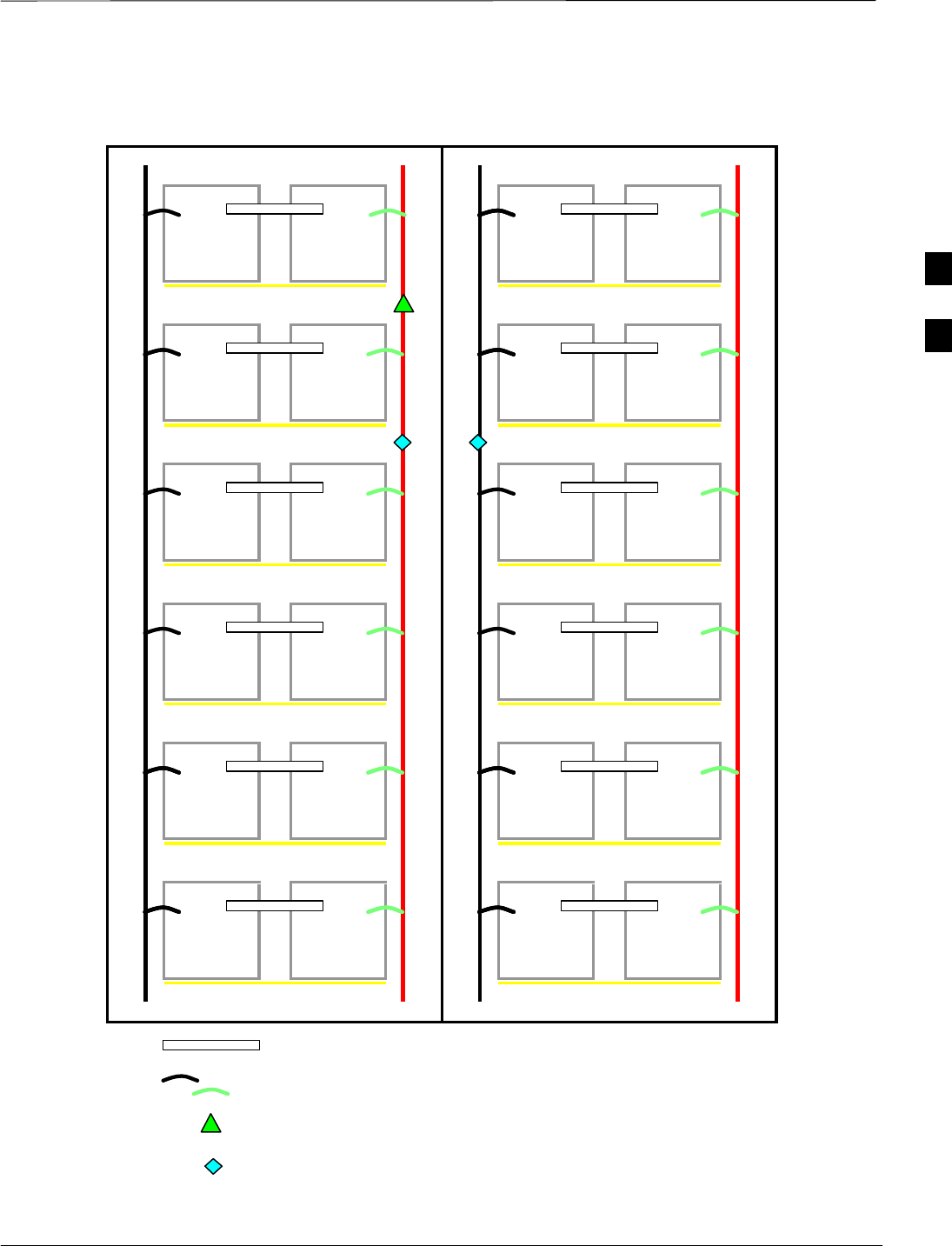
Alarms Testing – continued
Jan 2002 3-113
SCt4812ET BTS Optimization/ATP — CDMA LMF
Figure 3-24: Battery Overtemperature Sensor
Buss Bar
6 AWG Cables
Battery Overtemp Sensor
Negative Temperature Compensation Sensor
FW00408
3
Alarms Testing – continued
SCt4812ET BTS Optimization/ATP — CDMA LMF Jan 2002
3-114
Rectifier Over Temperature
Alarm
This is connector J8 on the rear of the Meter Alarm Panel
itself, this is not connector J8 on the connector bulkhead at
the rear of the cabinet.
NOTE
Table 3-63 gives instructions on testing the battery over temperature
alarm system.
Table 3-63: Rectifier Over Temperature Alarm
Step Action
1Remove the J8 link on the rear of the Meter Alarm Panel (see Figure 3-25 for J8 location).
NOTE
This is the J8 on the rear of the Meter Alarm Panel itself, this is not connector J8 on the connector
bulkhead at the rear of the cabinet.
2Verify that RECTIFIER OVERTEMP LED (red) is lite. Contacts on K1 and K2 change states (K1
now closed and K2 open).
3Verify that the LMF has reported an alarm condition. (BTS #26)
4Reinstall J8 connector and verify that all alarm conditions have cleared. K1 and K2 should now be in
their normal states (K1 open and K2 closed).
5This completes the system tests of the SC 4812ET power cabinet.
3
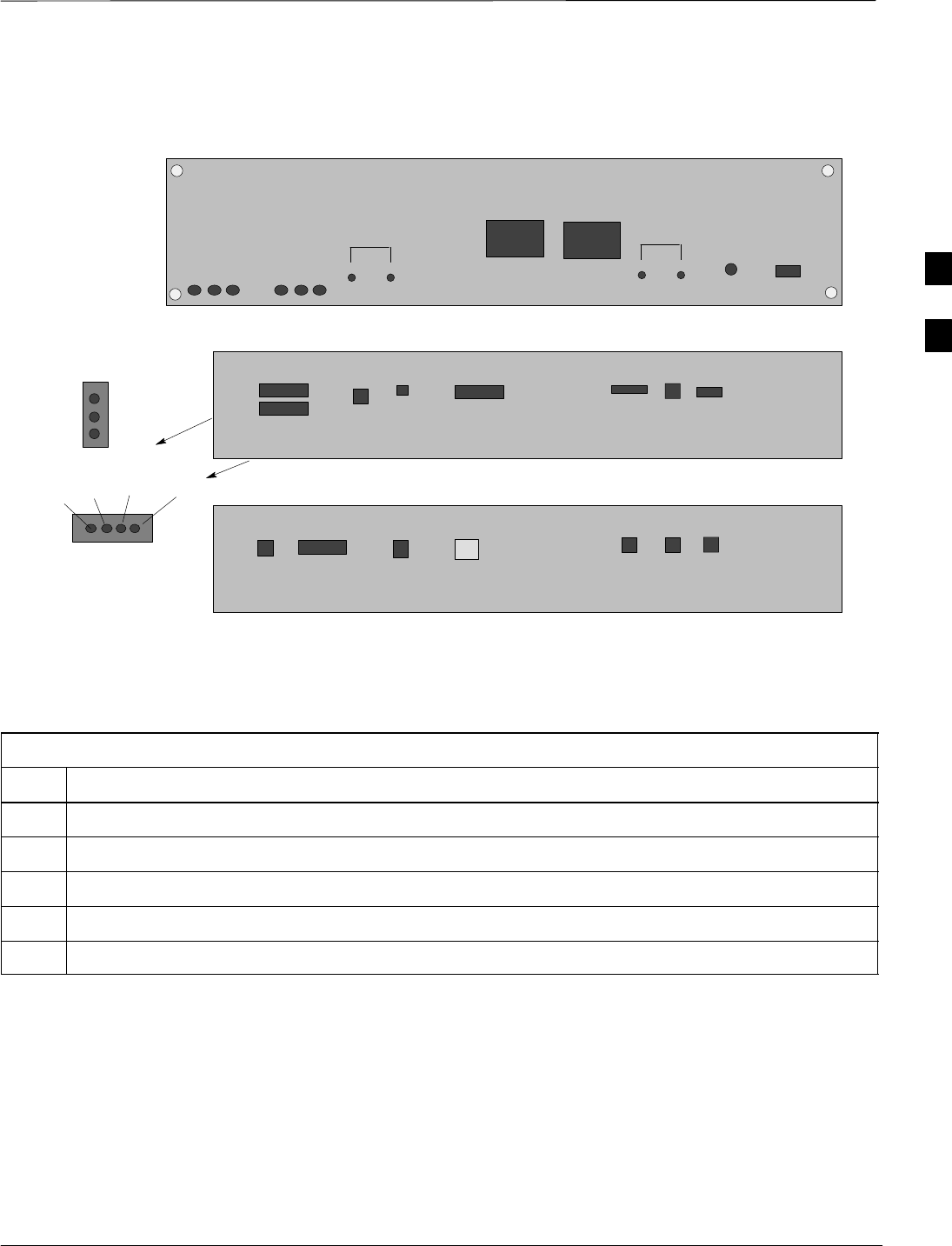
Alarms Testing – continued
Jan 2002 3-115
SCt4812ET BTS Optimization/ATP — CDMA LMF
Figure 3-25: Location of Connector J8 on the Meter Alarm Panel
OFF
VOLT
VOLT
–
+
TEST POINTS
AMPS
–
+
TEST POINTS
AMP
PWR
ON
RED
YEL
BLK
OR
VIOLENT
OR BRWN
Terminal Block
FRONT VIEW
J9
J1
J2
J3 J8 J5
J6 J4
REAR VIEW
Terminal Block
J1 J2
Not
Used
J6
J5 J3
Rear Connector Panel
J4
FW00245
Before Leaving the site
Table 3-64 gives instructions on what to check before leaving the site.
Table 3-64: Check Before Leaving the Site
Step Action
1Verify that ALL battery circuit breakers (for occupied shelves) are CLOSED (pushed in).
2Verify that the Heat Exchanger is running.
3Verify that the Meter Alarm Panel and TCP modules are switched ON.
4Verify that the Battery Test Switch on the Meter Alarm Panel is in the OFF position.
5Verify that no alarm conditions are being reported (with all doors closed).
3

Alarms Testing – continued
SCt4812ET BTS Optimization/ATP — CDMA LMF Jan 2002
3-116
Notes
3

Jan 2002 SCt4812ET BTS Optimization/ATP — CDMA LMF
Chapter 4: Automated Acceptance Test Procedure (ATP)
Table of Contents
Automated Acceptance Test Procedures – Overview 4-1. . . . . . . . . . . . . . . . . . . . .
Introduction 4-1. . . . . . . . . . . . . . . . . . . . . . . . . . . . . . . . . . . . . . . . . . . . . .
ATP Tests Prerequisites 4-2. . . . . . . . . . . . . . . . . . . . . . . . . . . . . . . . . . . . .
TX/RX OUT Connections 4-2. . . . . . . . . . . . . . . . . . . . . . . . . . . . . . . . . . .
ATP Test Procedure 4-3. . . . . . . . . . . . . . . . . . . . . . . . . . . . . . . . . . . . . . . .
CDMA 2000 Testing 4-3. . . . . . . . . . . . . . . . . . . . . . . . . . . . . . . . . . . . . . .
Individual Acceptance Tests 4-4. . . . . . . . . . . . . . . . . . . . . . . . . . . . . . . . .
TX Spectral Purity Transmit Mask Acceptance Test 4-6. . . . . . . . . . . . . . . . . . . . .
Background: Tx Mask Test 4-6. . . . . . . . . . . . . . . . . . . . . . . . . . . . . . . . . .
TX Waveform Quality (rho) Acceptance Test 4-8. . . . . . . . . . . . . . . . . . . . . . . . . .
Background: Rho Test 4-8. . . . . . . . . . . . . . . . . . . . . . . . . . . . . . . . . . . . . .
TX Pilot Time Offset Acceptance Test 4-9. . . . . . . . . . . . . . . . . . . . . . . . . . . . . . . .
Background: Pilot Offset Acceptance Test 4-9. . . . . . . . . . . . . . . . . . . . . .
TX Code Domain Power Acceptance Test 4-10. . . . . . . . . . . . . . . . . . . . . . . . . . . . .
Background: Code Domain Power Test 4-10. . . . . . . . . . . . . . . . . . . . . . . .
RX Frame Error Rate (FER) Acceptance Test 4-12. . . . . . . . . . . . . . . . . . . . . . . . . .
Background: FER Test 4-12. . . . . . . . . . . . . . . . . . . . . . . . . . . . . . . . . . . . . .
Generate an ATP Report 4-13. . . . . . . . . . . . . . . . . . . . . . . . . . . . . . . . . . . . . . . . . . .
Background 4-13. . . . . . . . . . . . . . . . . . . . . . . . . . . . . . . . . . . . . . . . . . . . . .
ATP Report 4-13. . . . . . . . . . . . . . . . . . . . . . . . . . . . . . . . . . . . . . . . . . . . . .
4

Table of Contents – continued
SCt4812ET BTS Optimization/ATP — CDMA LMF Jan 2002
Notes
4
Automated Acceptance Test Procedures – Overview
Jan 2002 4-1
SCt4812ET BTS Optimization/ATP — CDMA LMF
Introduction
The Automated Acceptance Test Procedure (ATP) allows Motorola
Cellular Field Engineers (CFEs) to run automated acceptance tests on all
equipped BTS subsystem devices using the Local Maintenance Facility
(LMF) and supported test equipment per the current Cell Site Data File
(CDF) assignment.
The results of these tests (at the option of the operator) are written to a
file that can be printed. All tests are controlled via the LMF platform
using the GPIB interface, therefore, only recommended test equipment
supported by the LMF can be used.
This chapter describes the tests run from the GUI environment, which is
the recommended method. The GUI provides the advantages of
simplifying the LMF user interface, reducing the potential for miskeying
commmands and associated parameters, and speeding up the execution
of complex operations involving multiple command strings. If you feel
the command line interface (CLI) will provide additional insight into the
progress of ATPs and problems that could possibly be encountered, refer
to LMF CLI Commands.
Before using the LMF, use an editor to view the
”CAVEATS” section in the ”readme.txt” file in the c:\wlmf
folder for any applicable information.
The ATP test is to be performed on out-of-service sectors
only.
DO NOT substitute test equipment with other models not
supported by the LMF.
IMPORTANT
*
4

Automated Acceptance Test Procedure – Overview – continued
SCt4812ET BTS Optimization/ATP — CDMA LMF Jan 2002
4-2
Reduced ATP
Equipment has been factory–tested for FCC compliance. If
license–governing bodies require documentation
supporting SITE compliance with regulations, a full ATP
may be necessary. Perform the Reduced ATP only if
reports for the specific BTS site are NOT required.
NOTE
After downloading the proper operational software to the BTS, the
Cellular Field Engineer (CFE) must perform these procedures (minimal
recommendation):
1 Verify the TX/RX paths by performing TX Calibration, TX Audit
and FER tests.
2 Retrieve Calibration Data required for normal site operation.
Should failures occur while performing the specified tests, refer to the
Basic Troubleshooting section of this manual for help in determining the
failure point. Once the point of failure has been identified and corrected,
refer to the BTS Optimization and ATP Test Matrix section (Table B-1)
to determine the applicable test that must be performed.
In the unlikely event that the BTS passes these tests but has a forward
link problem during normal operation, the CFE should then perform the
additional TX tests for troubleshooting: TX spectral mask, TX rho, and
TX code domain.
Refer to Chapter 3 for detailed information on test set
connections for calibrating equipment, cables and other test
set components, if required.
NOTE
Customer requirements determine which ATP tests to are to be
performed and the field engineer selects the appropriate ATP tests to run.
The tests can be run individually or as one of the following groups:
SAll TX: TX tests verify the performance of the BTS transmit line up.
These include the GLI2, MCC, BBX, and CIO cards, the LPAs and
passive components including splitters, combiners, bandpass filter,
and RF cables.
SAll RX: RX tests verify the performance of the BTS receiver line up.
These includes the MPC (for starter frames), EMPC (for expansion
frames), CIO, BBX, MCC, and GLI2 cards and the passive
components including RX filter (starter frame only), and RF cables.
SAll TX/RX: Executes all the TX and RX tests.
4
Automated Acceptance Test Procedure – Overview – continued
Jan 2002 4-3
SCt4812ET BTS Optimization/ATP — CDMA LMF
SFull Optimization: Executes the TX calibration, download BLO, and
TX audit before running all of the TX and RX tests.
ATP Test Prerequisites
Before attempting to run any ATP tests, ensure the following:
SBTS has been optimized and calibrated (see Chapter 3).
SLMF is logged into the BTS.
SCSMs, GLI2s, BBXs, MCCs and TSU (if the RFDS is installed)have
correct code load and data load
SPrimary CSM and GLI2 are INS_ACT
SMCCs are INS_ACT.
SBBXs are OOS-RAM.
SBBXs are calibrated and BLOs are downloaded.
STest cables are calibrated.
STest equipment is selected.
STest equipment is connected for ATP tests.
STest equipment has been warmed up 60 minutes and calibrated.
SGPIB is on.
Before the FER is run, be sure that all LPAs are turned
OFF (circuit breakers pulled) or that all transmitter ports
are properly terminated.
All transmit ports must be properly terminated for all ATP
tests.
Failure to observe these warnings may result in bodily
injury or equipment damage.
WARNING
TX/RX OUT Connections
Many of the acceptance test procedures require taking
measurements at the TX OUT (BTS/RFDS) connector. At
sites with RFDS, all measurements are through the RFDS
directional coupler TX OUT connector.
IMPORTANT
*
4
Automated Acceptance Test Procedure – Overview – continued
SCt4812ET BTS Optimization/ATP — CDMA LMF Jan 2002
4-4
ATP Test Procedure
There are three different ATP testing options that can be performed to
completely test a BTS. Depending on your requirements, one of the
following ATP testing options should be run. Table 4-1 provides the
procedure to execute an ATP test. To completely test a BTS, run the ATP
tests according to one of the following ATP testing options.
ATP Testing Option 1
SAll TX/RX test
ATP Testing Option 2
SAll TX test
SAll RX test
ATP Testing Option 3
STX Mask test
SRho test
SPilot Time Offset test
SCode Domain Power test
SFER test
The Full Optimization test can be run if you want the TX
path calibrated before all the TX and RX tests are run.
NOTE
If manual testing has been performed with the HP analyzer,
remove the manual control/system memory card from the
card slot and set the IO CONFIG to the Talk & Listen
mode before starting the automated testing.
IMPORTANT
*
CDMA 2000 Testing
Software release 2.16.x supports two new pieces of test equipment.
These are the Agilent E4406A with E4432B, as well as the Advantest
R3267 with R3562. The E4406A/E4432B pair, or the R3267/R3562
pair, should be connected together using a GPIB cable. This test
equipment is capable of performing tests in both IS95 mode as well as
cdma2000 mode if the required options are installed:
The HP 8935 with option 200 or R2k for 1X TX and with Agilent
E4432B Signal Generator for 1X FER
4

Automated Acceptance Test Procedure – Overview – continued
Jan 2002 4-5
SCt4812ET BTS Optimization/ATP — CDMA LMF
Individual Acceptance Tests The following individual ATP tests can be used to verify the results of
specific tests:
Spectral Purity TX Mask
This test verifies that the transmitted CDMA carrier waveform,
generated on each sector, meets the transmit spectral mask specification
with respect to the assigned CDF file values.
Waveform Quality (rho)
This test verifies that the transmitted Pilot channel element digital
waveform quality (rho) exceeds the minimum specified value in
ANSI–J_STD–019. “Rho” represents the correlation between actual and
perfect CDMA modulation spectrum. A rho value of 1.0000 represents
100% (or perfect correlation).
Pilot Time Offset
The Pilot Time Offset is the difference between the CDMA analyzer
measurement interval (based on the BTS system time reference) and the
incoming block of transmitted data from the BTS (Pilot only, Pilot
Gain = 262, PN Offset = 0).
Code Domain Power
This test verifies code domain power levels, which have been set for all
ODD numbered Walsh channels, using the OCNS command. This is
done by verifying that the ratio of PILOT divided by OCNS is equal to
10.2 + 2 dB, and, that the noise floor of all EVEN numbered “OFF”
Walsh channels measures < –27 dB .
Frame Error Rate
The Frame Error Rate (FER) test verifies RX operation of the entire
CDMA Reverse Link using all equipped MCCs assigned to all
respective sector/antennas. The test verifies the BTS sensitivity on all
traffic channel elements currently configured on all equipped MCCs at
an RF input level of –119 dBm (or –116 dBm if using TMPC). Follow
the procedure in Table 4-1 to perform any ATP test.
The STOP button can be used to stop the testing process.
NOTE
4

Automated Acceptance Test Procedure – Overview – continued
SCt4812ET BTS Optimization/ATP — CDMA LMF Jan 2002
4-6
ATP Test Procedure Table 4-1 describes the step–by–step procedures to run any APT Test.
Table 4-1: ATP Test Procedure
Step Action
1Select the device(s) to be tested.
2From the Tests menu, select the desired test.
3Select the appropriate carrier(s) (carrier – bts# – sector# – carrier#) displayed in the Channels/Carrier
pick list.
To select multiple items, hold down the <Shift> or <Ctrl> key while making the selections.
4Type the appropriate channel number in the Carrier n Channels box.
The default channel number displayed is determined by the CdmaChans[n] number in the cbsc–n.cdf
file for the BTS.
5If applicable, select Verify BLO (default) or Single–sided BLO.
NOTE
Single–sided BLO is only used when checking non–redundant transceivers.
6For RX select the appropriate RX branch (Both, Main, or Diversity) in the drop–down list.
7In the Rate Set box, select the appropriate data rate (1=9600, 2=14400, 3=9600 1X) from the
drop–down list.
NOTE
The Rate Set selection of 3 is only available if 1X cards are selected for the test.
8In the Test Pattern box, select the test pattern to use for the calibration from the drop–down list: Pilot
(default), CDF, CDFPilot or Standard.
9 Click OK.
The status report window and a Directions pop-up are displayed.
10 Follow the cable connection directions as they are displayed.
11 Click Save Results or Dismiss to close the status report window.
If Dismiss is used the test results will not be saved in the test report file.
4

TX Spectral Purity Transmit Mask Acceptance Test
Jan 2002 4-7
SCt4812ET BTS Optimization/ATP — CDMA LMF
Background: Tx Mask Test
This test verifies the spectral purity of each BBX2 carrier keyed up at a
specific frequency, per the current CDF file assignment. All tests are
performed using the external calibrated test set, controlled by the same
command. All measurements are through the appropriate TX OUT
(BTS/RFDS) connector.
The Pilot Gain is set to 541 for each antenna and all channel elements
from the MCCs are forward-link disabled. The BBX2 is keyed up, using
both bbxlvl and bay level offsets, to generate a CDMA carrier (with pilot
channel element only). BBX2 power output is set to obtain +40 dBm as
measured at the TX OUT connector (on either the BTS or RFDS
directional coupler).
TX output power is set to +40 dBm by setting BTS power
level to +33.5 dBm to compensate for 6.5 dB increase from
pilot gain set to 541.
NOTE
The calibrated communications test set measures and returns the
attenuation level of all spurious and IM products in a 30 kHz resolution
bandwidth with respect to the mean power of the CDMA channel,
measured in a 1.23 MHz bandwidth, in dB, verifying that results meet
system tolerances at the following test points:
S1.9 GHz
–at least –45 dB @ + 900 kHz from center frequency
–at least –45 dB @ – 900 kHz from center frequency
S800 MHz:
–at least –45 dB @ + 750 kHz from center frequencY
–at least –45 dB @ – 750 kHz from center frequency
–at least –60 dB @ – 1980 kHz from center frequency
–at least –60 dB @ – 1980 kHz from center frequency
The BBX2 then de-keys, and, if selected, the MCC is re-configured to
assign the applicable redundant BBX2 to the current TX antenna path
under test. The test is then repeated.
4
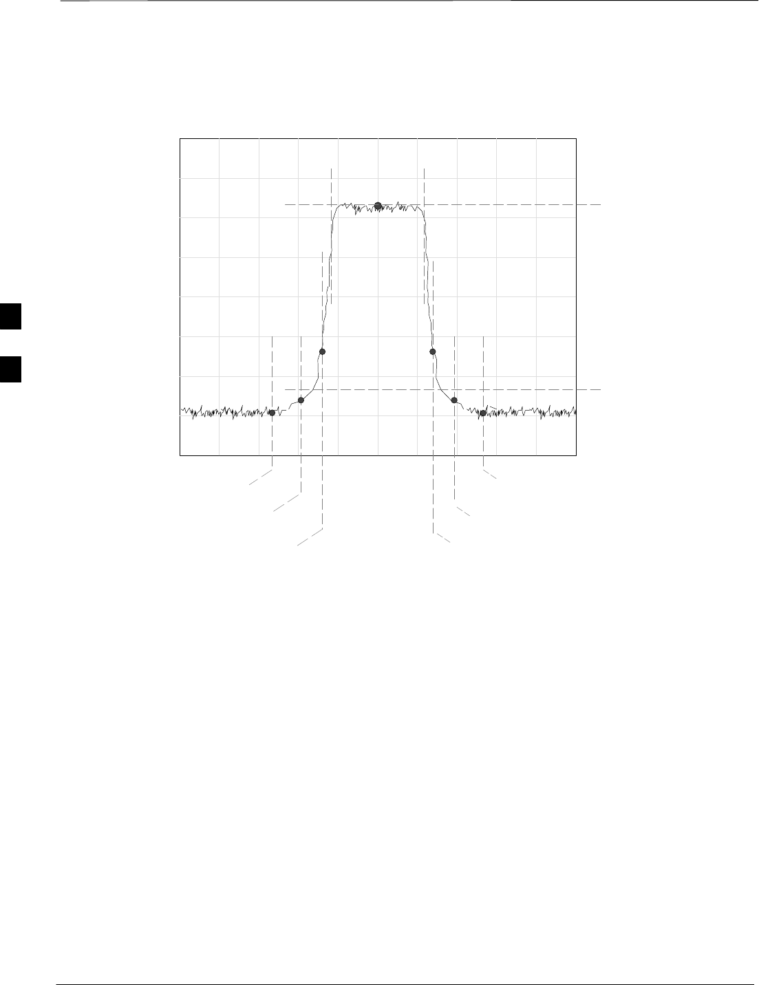
TX Spectral Purity Transmit Mask Acceptance Test – continued
SCt4812ET BTS Optimization/ATP — CDMA LMF Jan 2002
4-8
Figure 4-1: TX Mask Verification Spectrum Analyzer Display
– 900 kHz + 900 kHz
Center Frequency
Reference
Attenuation level of all
spurious and IM products
with respect to the mean
power of the CDMA channel
.5 MHz Span/Div
Ampl 10 dB/Div
Mean CDMA Bandwidth
Power Reference
+750 kHz
+ 1980 kHz
– 750 kHz
– 1980 kHz
FW00282
4

TX Waveform Quality (rho) Acceptance Test
Jan 2002 4-9
SCt4812ET BTS Optimization/ATP — CDMA LMF
Background: Rho Test
This test verifies the transmitted Pilot channel element digital waveform
quality of each BBX2 carrier keyed up at a specific frequency per the
current CDF file assignment. All tests are performed using the external
calibrated test set controlled by the same command. All measurements
are via the appropriate TX OUT (BTS/RFDS) connector.
The Pilot Gain is set to 262 for each antenna, and all channel elements
from the MCCs will be forward link disabled. The BBX2 is keyed up
using both bbxlvl and bay level offsets, to generate a CDMA carrier
(with pilot channel element only, Walsh code 0). BBX2 power output is
set to 40 dBm as measured at the TX OUT connector (on either the BTS
or RFDS directional coupler).
The calibrated communications test set measures and returns the Pilot
channel element digital waveform quality (rho) in dB, verifying that
result meets system tolerances Waveform quality (rho) should
be > 0.912 (–0.4 dB).
The BBX2 then de-keys and the applicable redundant BBX2 is assigned
to the current TX antenna path under test. The test is then repeated.
The LMF Tests menu list item, Rho, performs the waveform quality test
for a XCVR(s). All measurements are made through the appropriate TX
output connector using the calibrated TX cable setup.
4

TX Pilot Time Offset Acceptance Test
SCt4812ET BTS Optimization/ATP — CDMA LMF Jan 2002
4-10
Background: Pilot Offset
Acceptance Test
This test verifies the transmitted Pilot channel element Pilot Time Offset
of each BBX2 carrier keyed up at a specific frequency per the current
CDF file assignment. All tests are performed using the external
calibrated test set controlled by the same command. All measurements
will be via the appropriate TX OUT (BTS/RFDS) connector.
The Pilot Gain is set to 262 for each antenna and all TCH elements from
the MCCs are forward link disabled. The BBX is keyed up using both
bbxlvl and bay level offsets to generate a CDMA carrier (with pilot
channel element only, Walsh code 0). BBX power output is set to
40 dBm as measured at the TX OUT connector (on either the BTS or
RFDS directional coupler).
The calibrated communications test set measures and returns the Pilot
Time Offset in uS, verifying results meet system tolerances: Pilot Time
Offset should be within < 3 µs of the target PT Offset (0 mS).
The BBX2 then de-keys, and the applicable redundant BBX2 is assigned
to the current TX antenna path under test. The test is then repeated.
4

TX Code Domain Power Acceptance Test
Jan 2002 4-11
SCt4812ET BTS Optimization/ATP — CDMA LMF
Background: Code Domain
Power Test
This test verifies the Code Domain Power/Noise of each BBX2 carrier
keyed up at a specific frequency per the current CDF file assignment.
All tests are performed using the external calibrated test set controlled by
the same command. All measurements are via the appropriate TX OUT
(BTS/RFDS) connector.
For each sector/antenna under test, the Pilot Gain is set to 262 and all
MCC channel elements under test are configured to generate Orthogonal
Channel Noise Source (OCNS) on different odd Walsh codes, and are
assigned a full–rate gain of 81. The maximum number of MCC/CEs to
be tested an any one time is 32 (32 odd Walsh codes). If more than 32
CEs exist, then multiple sets of measurements are made, so all channel
elements are verified on all sectors.
BBX2 power output is set to 40 dBm as measured at the TX OUT
connector (on either the BTS or RFDS directional coupler).
Code domain power levels, which have been set for all ODD numbered
Walsh channels, are verified using the OCNS command. This is done by
verifying that Pilot Power (dBm) minus OCNS Power (dBm) is equal to
10.2 + 2 dB and that the noise floor of all “OFF” Walsh channels
measures < –27 dB (with respect to total CDMA channel power).
The BBX2 then de-keys and, the applicable redundant BBX2 is assigned
to the current TX antenna path under test. The test is then repeated.
Upon completion of the test, OCNS is disabled on the specified
MCC/CE.
4
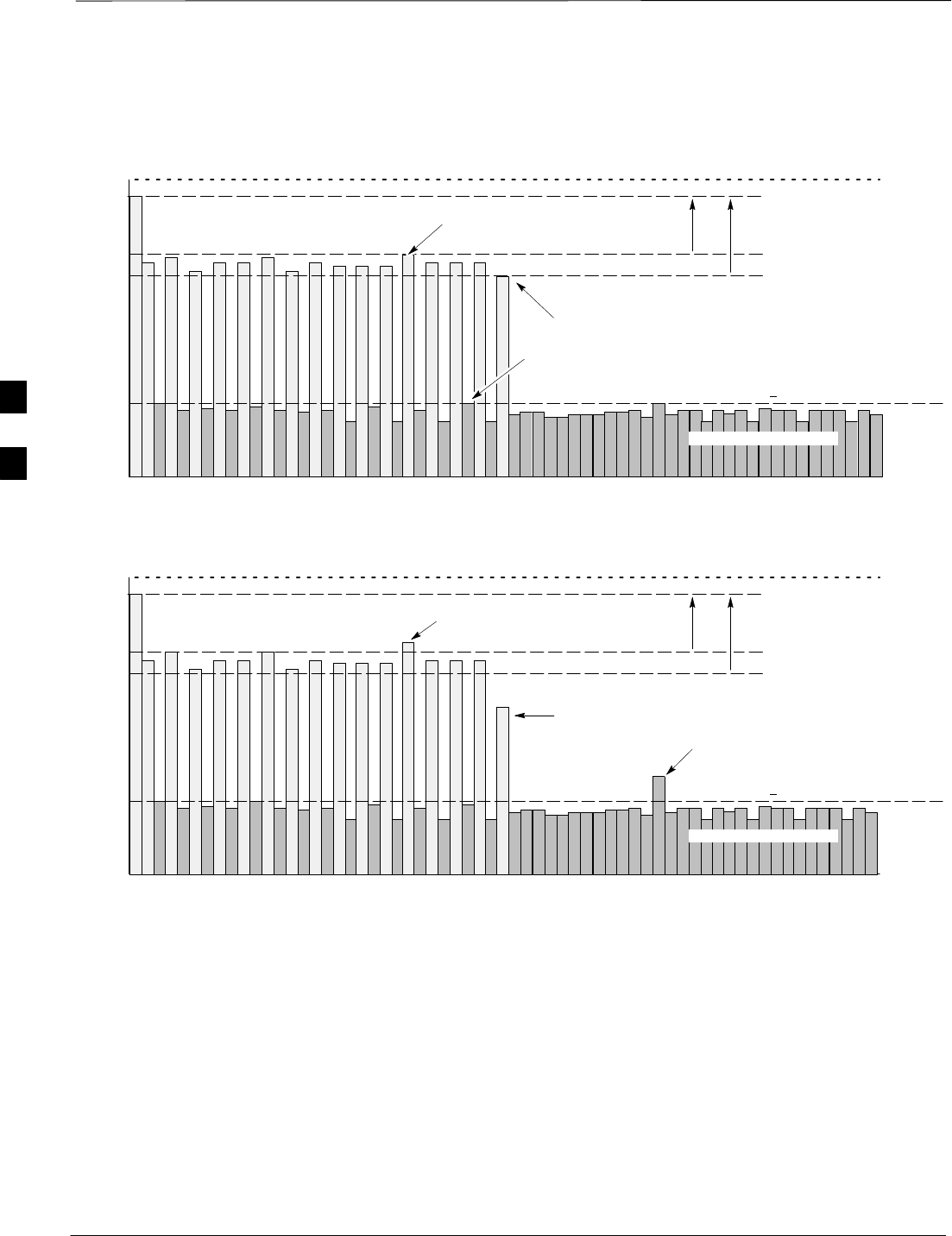
TX Code Domain Power Acceptance Test – continued
SCt4812ET BTS Optimization/ATP — CDMA LMF Jan 2002
4-12
Pilot Channel
Active channels
PILOT LEVEL
MAX OCNS SPEC.
MIN OCNS SPEC.
MAXIMUM NOISE FLOOR:
< –27 dB SPEC.
Inactive channels
Walsh 0 1 2 3 4 5 6 7 ... 64
MAX OCNS
CHANNEL
MIN OCNS
CHANNEL
8.2 dB 12.2 dB
MAX NOISE
FLOOR
Pilot Channel
Active channels
PILOT LEVEL
MAX OCNS SPEC.
MIN OCNS SPEC.
MAXIMUM NOISE FLOOR:
< –27 dB
Inactive channels
Walsh 0 1 2 3 4 5 6 7 ... 64
FAILURE – DOES NOT
MEET MIN OCNS SPEC.
FAILURE – EXCEEDS
MAX OCNS SPEC. 8.2 dB 12.2 dB
FAILURE – EXCEEDS MAX
NOISE FLOOR SPEC.
Showing all OCNS Passing
Indicating Failures
Figure 4-2: Code Domain Power and Noise Floor Levels
FW00283
4

RX Frame Error Rate (FER) Acceptance Test
Jan 2002 4-13
SCt4812ET BTS Optimization/ATP — CDMA LMF
Background: FER Test
This test verifies the BTS FER on all traffic channel elements currently
configured on all equipped MCCs (full rate at 1% FER) at an RF input
level of –119 dBm [or –116 dBm if using Tower Top Amplifier
(TMPC)]. All tests are performed using the external calibrated test set as
the signal source controlled by the same command. All measurements
will be via the LMF.
The pilot gain is set to 262 for each TX antenna and all channel elements
from the MCCs are forward-link disabled. The BBX2 is keyed up using
only bbxlvl level offsets, to generate a CDMA carrier (with pilot channel
element only). BBX2 power output is set to –20 dBm as measured at the
TX OUT connector (on either the BTS or RFDS directional coupler).
The BBX2 must be keyed in order to enable the RX receive circuitry.
The LMF prompts the MCC/CE under test to measure all zero longcode
and provide the FER report on the selected active MCC on the reverse
link for both the main and diversity RX antenna paths, verifying the
results meet the following specification: FER returned less than 1% and
total frames measured is 1500.
All MCC/CEs selected are tested on the specified RX antenna path. The
BBX then de-keys and, the applicable redundant BBX2 is assigned to
the current RX antenna paths under test. The test is then repeated.
4

Generate an ATP Report
SCt4812ET BTS Optimization/ATP — CDMA LMF Jan 2002
4-14
Background
Each time an ATP test is run, an ATP report is updated to include the
results of the most recent ATP tests if the Save Results button is used to
close the status report window. The ATP report will not be updated if the
status reports window is closed with use of the Dismiss button.
ATP Report
A separate report is created for each BTS and includes the following for
each test:
STest name
SBBX number
SChannel number
SCarrier number
SSector number
SUpper test limit
SLower test limit
STest result
SPASS or FAIL
SDescription information (if applicable)
STime stamp
SDetails/Warning information (if applicable)
Follow the procedure in the Table 4-2 to view and create a printable file
for the ATP report of a BTS.
Table 4-2: Generate an ATP Report
Step Action
1Click on the Login tab if it is not in the forefront.
2Select the desired BTS from the Available Base Stations pick list.
3Click on the Report button.
4Sort the report if desired by clicking on a column heading.
5Click on the Dismiss button if you do not want to create a printable file copy.
6To create a printable file, select the desired file type in the picklist and then click on the Save button.
4

Jan 2002 SCt4812ET BTS Optimization/ATP — CDMA LMF
Chapter 5: Leaving the Site
Table of Contents
External Test Equipment Removal 5-1. . . . . . . . . . . . . . . . . . . . . . . . . . . . . . . . . . .
Reset All Devices 5-1. . . . . . . . . . . . . . . . . . . . . . . . . . . . . . . . . . . . . . . . . . . . . . . .
Updating BTS CAL LMF Files in the CBSC 5-1. . . . . . . . . . . . . . . . . . . . . . . . . .
BTS Site Span Configuration Verification 5-3. . . . . . . . . . . . . . . . . . . . . . . . . . . . .
Set BTS Site Span Configuration 5-4. . . . . . . . . . . . . . . . . . . . . . . . . . . . . . . . . . . .
Re–connect BTS T1 Spans and Integrated Frame Modem 5-6. . . . . . . . . . . . . . . .
LMF Removal 5-6. . . . . . . . . . . . . . . . . . . . . . . . . . . . . . . . . . . . . . . . . . . . . . . . . . .
Reestablish OMC-R Control/ Verifying T1/E1 5-7. . . . . . . . . . . . . . . . . . . . . . . . . 5

Table of Contents – continued
SCt4812ET BTS Optimization/ATP — CDMA LMF Jan 2002
Notes
5