Nokia Solutions and Networks T5CT1 Cellular CDMA base station User Manual IHET5CT1 GLI2 Manual 5 of 6
Nokia Solutions and Networks Cellular CDMA base station IHET5CT1 GLI2 Manual 5 of 6
Contents
- 1. IHET5CT1 GLI2 Manual 1 of 6
- 2. IHET5CT1 GLI2 Manual 2 of 6
- 3. IHET5CT1 GLI2 Manual 3 of 6
- 4. IHET5CT1 GLI2 Manual 4 of 6
- 5. IHET5CT1 GLI2 Manual 5 of 6
- 6. IHET5CT1 GLI2 Manual 6 of 6
- 7. IHET5CT1 GLI3 Manual 1 of 6
- 8. IHET5CT1 GLI3 Manual 4 of 6
- 9. IHET5CT1 GLI3 Manual 5 of 6
- 10. IHET5CT1 GLI3 Manual 6 of 6
IHET5CT1 GLI2 Manual 5 of 6
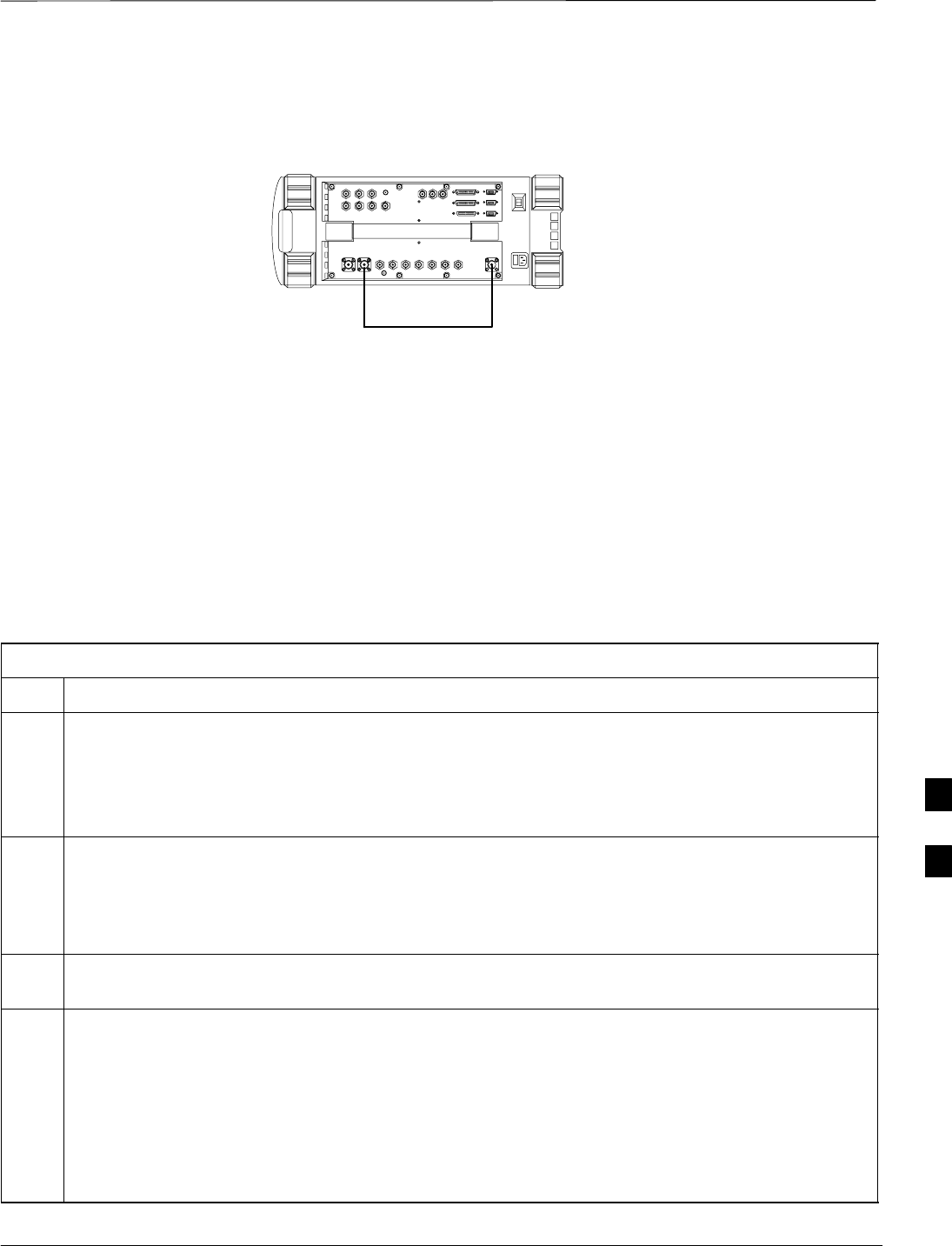
Test Equipment Preparation – continued
SCt4812ET BTS Optimization/ATP — CDMA LMF Jan 2002
F-10
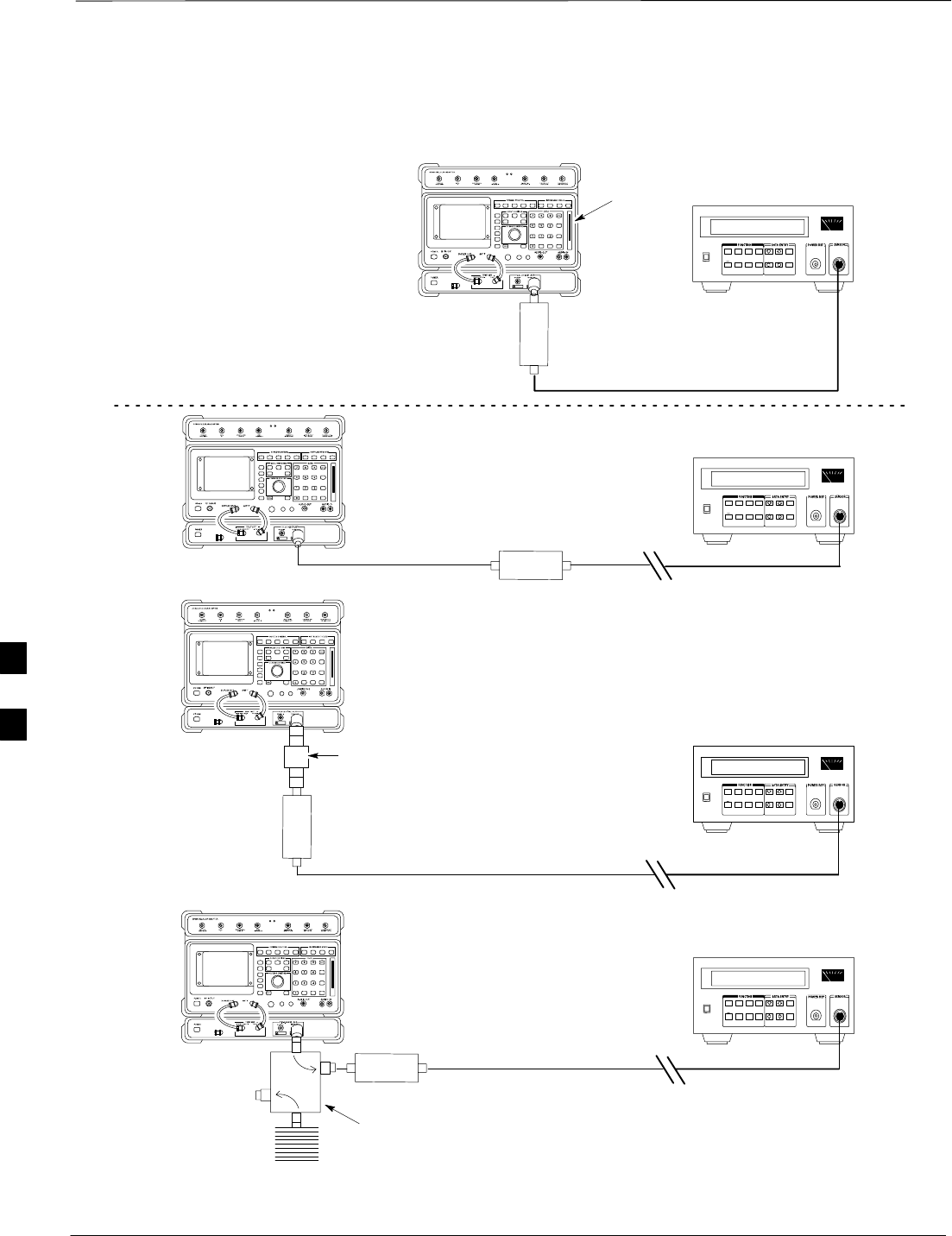
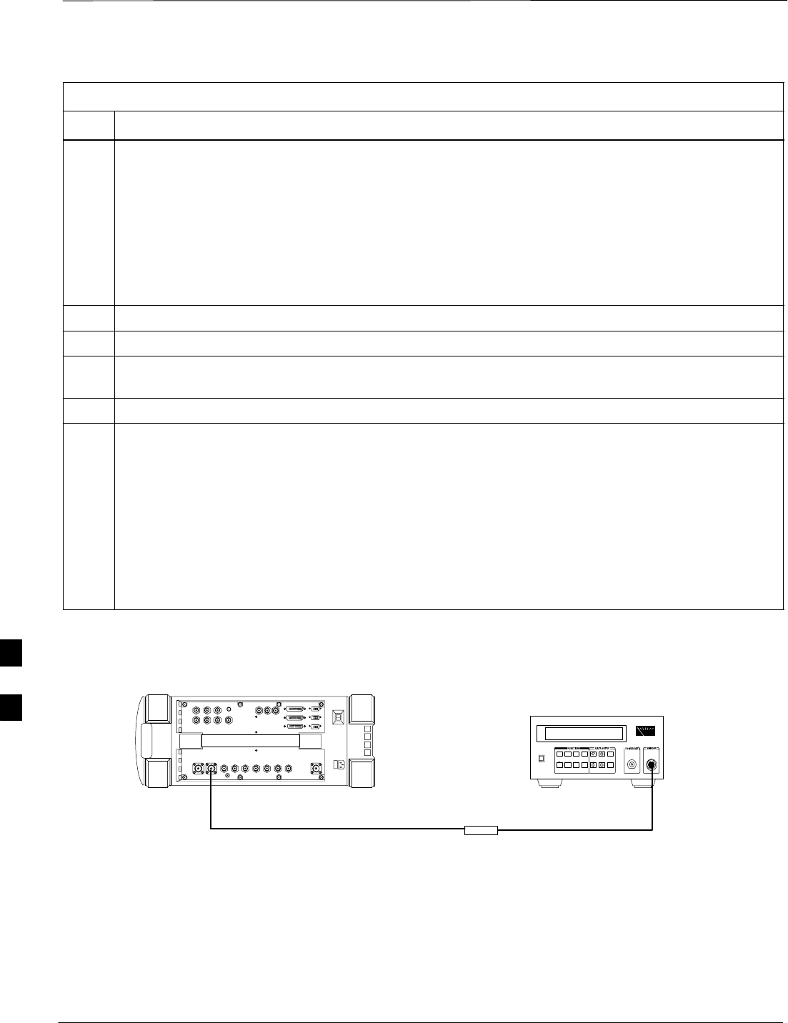
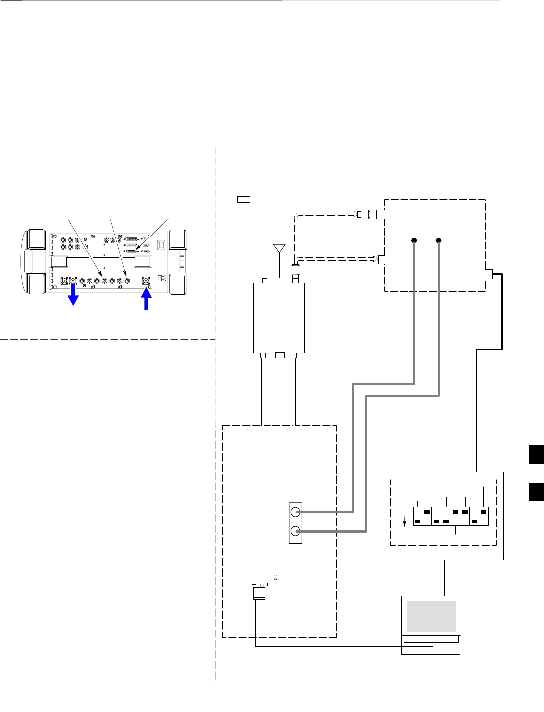
Agilent E4406A/E4432B Test
Equipment Interconnection
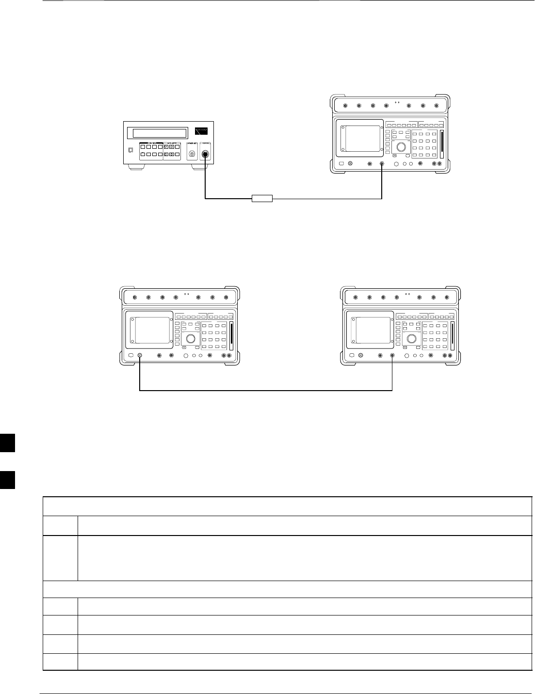
To provide proper operation during testing when both units are required,
the 10 MHz reference signal from the E4406A transmitter test set must
be provided to the E4432B signal generator. Connect a BNC (M)–BNC
(M) cable from the E4406A 10 MHz OUT (SWITCHED) connector to
the E4432B 10MHz IN connector as shown in Figure F-5.
Figure F-5: Agilent 10 MHz Reference Connections
E4406A
10 MHz OUT
(SWITCHED)
E4432B
10 MHz IN
TO GPIB BOX
F
Manual Cable Calibration
Jan 2002 F-11
SCt4812ET BTS Optimization/ATP — CDMA LMF
Calibrating Test Cable Setup
using HP PCS Interface (HP83236)
Table F-9 covers the procedure to calibrate the test equipment using
the HP8921 Cellular Communications Analyzer equipped with the
HP83236 PCS Interface.
This calibration method must be executed with great care.
Some losses are measured close to the minimum limit of
the power meter sensor (–30 dBm).
NOTE
Prerequisites
Ensure the following prerequisites have been met before proceeding:
STest equipment to be calibrated has been connected correctly for cable
calibration.
STest equipment has been selected and calibrated.
Table F-9: Calibrating Test Cable Setup (using the HP PCS Interface)
Step Action
NOTE
Verify that GPIB controller is turned off.
1Insert HP83236 Manual Control System card into memory card slot.
2Press the Preset pushbutton.
3 Under Screen Controls, press the TESTS pushbutton to display the TESTS (Main Menu) screen.
4Position the cursor at Select Procedure Location and select it. In the Choices selection box, select
CARD.
5Position the cursor at Select Procedure Filename and select it. In the Choices selection box, select
MANUAL.
6Position the cursor at RUN TEST and select it. HP must be in Control Mode Select YES.
7If using HP 83236A:
Set channel number=<chan#>:
–Position cursor at Channel
Number and select it.
–Enter the chan# using the numeric
keypad; press [Enter] and the
screen will go blank.
–When the screen reappears, the
chan# will be displayed on the
channel number line.
If using HP 83236B:
Set channel frequency:
–Position cursor at Frequency Band and press Enter.
–Select User Defined Frequency.
–Go Back to Previous Menu.
–Position the cursor to 83236 generator frequency and
enter actual RX frequency.
–Position the cursor to 83236 analyzer frequency and
enter actual TX frequency.
. . . continued on next page
F

Manual Cable Calibration – continued
SCt4812ET BTS Optimization/ATP — CDMA LMF Jan 2002
F-12
Table F-9: Calibrating Test Cable Setup (using the HP PCS Interface)
Step Action
8Set RF Generator level:
–Position the cursor at RF Generator Level and select it.
–Enter –10 using the numeric keypad; press [Enter] and the screen will go blank.
–When the screen reappears, the value –10 dBm will be displayed on the RF Generator Level line.
9Set the user fixed Attenuation Setting to 0 dBm:
–Position cursor at Analyzer Attenuation and select it
–Position cursor at User Fixed Atten Settings and select it.
–Enter 0 (zero) using the numeric keypad and press [Enter].
10 Select Back to Previous Menu.
11 Record the HP83236 Generator Frequency Level:
Record the HP83236B Generator Frequency Level:
–Position cursor at Show Frequency and Level Details and select it.
–Under HP83236 Frequencies and Levels, record the Generator Level.
–Under HP83236B Frequencies and Levels, record the Generator Frequency Level (1850 – 1910
MHz).
–Position cursor at Prev Menu and select it.
12 Click on Pause for Manual Measurement.
13 Connect the power sensor directly to the RF OUT ONLY port of the PCS Interface.
14 On the HP8921A, under To Screen, select CDMA GEN.
15 Move the cursor to the Amplitude field and click on the Amplitude value.
16 Increase the Amplitude value until the power meter reads 0 dBm ±0.2 dB.
NOTE
The Amplitude value can be increased coarsely until 0 dBM is reached; then fine tune the amplitude
by adjusting the Increment Set to 0.1 dBm and targeting in on 0 dBm.
17 Disconnect the power sensor from the RF OUT ONLY port of the PCS Interface.
* IMPORTANT
The Power Meter sensor’s lower limit is –30 dBm. Thus, only components having losses ≤30 dB
should be measured using this method. For further accuracy, always re-zero the power meter
before connecting the power sensor to the component being calibrated. After connecting the
power sensor to the component, record the calibrated loss immediately.
18 Disconnect all components in the test setup and calibrate each one separately by connecting each
component, one-at-a-time, between the RF OUT ONLY PORT and the power sensor. Record the
calibrated loss value displayed on the power meter.
SExample: (A) Test Cable(s) = –1.4 dB
(B) 20 dB Attenuator = –20.1 dB
(B) Directional Coupler = –29.8 dB
. . . continued on next page
F

Manual Cable Calibration – continued
Jan 2002 F-13
SCt4812ET BTS Optimization/ATP — CDMA LMF
Table F-9: Calibrating Test Cable Setup (using the HP PCS Interface)
Step Action
19 After all components are calibrated, reassemble all components together and calculate the total test
setup loss by adding up all the individual losses:
SExample: Total test setup loss = –1.4 –29.8 –20.1 = –51.3 dB.
This calculated value will be used in the next series of tests.
20 Under Screen Controls press the TESTS button to display the TESTS (Main Menu) screen.
21 Select Continue (K2).
22 Select RF Generator Level and set to –119 dBm.
23 Click on Pause for Manual Measurement.
24 Verify the HP8921A Communication Analyzer/83203A CDMA interface setup is as follows (fields
not indicated remain at default):
SVerify the GPIB (HP–IB) address:
–under To Screen, select More
–select IO CONFIG
–Set HP–IB Adrs to 18
–set Mode to Talk&Lstn
SVerify the HP8921A is displaying frequency (instead of RF channel)
–Press the blue [SHIFT] button, then press the Screen Control [DUPLEX] button; this switches to
the CONFIG (CONFIGURE) screen.
–Use the cursor control to set RF Display to Freq
25 Refer toChapter 3 for assistance in setting the cable loss values into the LMF.
F
Manual Cable Calibration – continued
SCt4812ET BTS Optimization/ATP — CDMA LMF Jan 2002
F-14
(A)
(C)
POWER
SENSOR
(A)
POWER
SENSOR
(C)
30 dB
DIRECTIONAL
COUPLER
150 W
NON–RADIATING
RF LOAD
POWER
SENSOR
(B)
POWER
SENSOR
(B)
MEMORY
CARD
SLOT
20 dB / 20 WATT
ATTENUATOR
FW00292
Figure F-6: Cable CalibrationUsing HP8921 with PCS Interface
F

Manual Cable Calibration – continued
Jan 2002 F-15
SCt4812ET BTS Optimization/ATP — CDMA LMF
Calibrating Test Cable Setup
using Advantest R3465
Be sure the GPIB Interface is OFF for this procedure.
NOTE
Advantest R3465 Manual Test setup and calibration must be performed
at both the TX and RX frequencies.
Table F-10: Procedure for Calibrating Test Cable Setup Using Advantest R3465
Step Action
* IMPORTANT
–This procedure can only be performed after test equipment has been allowed to warm–up and
stabilize for a minimum of 60 minutes.
1Press the SHIFT and the PRESET keys located below the display
2Press the ADVANCE key in the MEASUREMENT area of the control panel.
3Select the CDMA Sig CRT menu key
4Select the Setup CRT menu key
5Using the vernier knob and the cursor keys set the following parameters
NOTE
Fields not listed remain at default
Generator Mode: SIGNAL
Link: FORWARD
Level Unit: dBm
CalCorrection: ON
Level Offset: OFF
6Select the return CRT menu key
7 Press FREQ key in the ENTRY area
8Set the frequency to the desired value using the keypad entry keys
9Verify that the Mod CRT menu key is highlighting OFF; if not, press the Mod key to toggle it OFF.
10 Verify that the Output CRT menu key is highlighting OFF; if not, press the Output key to toggle it
OFF.
11 Press the LEVEL key in the ENTRY area.
12 Set the LEVEL to 0 dBm using the key pad entry keys.
13 Zero power meter. Next connect the power sensor directly to the “RF OUT” port on the R3561L
CDMA Test Source Unit.
14 Press the Output CRT menu key to toggle Output to ON.
15 Record the power meter reading ________________________
. . . continued on next page
F

Manual Cable Calibration – continued
SCt4812ET BTS Optimization/ATP — CDMA LMF Jan 2002
F-16
Table F-10: Procedure for Calibrating Test Cable Setup Using Advantest R3465
Step Action
16 Disconnect the power meter sensor from the R3561L RF OUT jack.
* IMPORTANT
The Power Meter sensor’s lower limit is –30 dBm. Thus, only components having losses < 30 dB
should be measured using this method. For best accuracy, always re–zero the power meter before
connecting the power sensor to the component being calibrated. Then, after connecting the
power sensor to the component, record the calibrated loss immediately.
17 Disconnect all components in the the test setup and calibrate each one separately. Connect each
component one–at–a–time between the “RF OUT” port and the power sensor (see Figure F-7, “Setups
A, B, and C”). Record the calibrated loss value displayed on the power meter for each connection.
Example: (A) 1st Test Cable = –0.5 dB
(B) 2nd Test Cable = –1.4 dB
(C) 20 dB Attenuator = –20.1 dB
(D) 30 dB Directional Coupler = –29.8 dB
18 Press the Output CRT menu key to toggle Output OFF.
19 Calculate the total test setup loss by adding up all the individual losses:
Example: Total test setup loss = 0.5 + 1.4 + 20.1 + 29.8 = 51.8 dB
This calculated value will be used in the next series of tests.
20 Press the FREQ key in the ENTRY area
21 Using the keypad entry keys, set the test frequency to the RX frequency
22 Repeat steps 9 through 19 for the RX frequency.
23 Refer to Chapter 3 for assistance in setting the cable loss values into the LMF.
F
Manual Cable Calibration – continued
Jan 2002 F-17
SCt4812ET BTS Optimization/ATP — CDMA LMF
POWER
SENSOR
20 DB / 2 WATT
ATTENUATOR
(A)
(C)
POWER
SENSOR
(D)
30 DB
DIRECTIONAL
COUPLER
(C)
100 W
NON–RADIATING
RF LOAD
POWER
SENSOR
RF OUT
POWER
SENSOR
& (B)
FW00320
Figure F-7: Cable Calibration using Advantest R3465
F
Manual Cable Calibration – continued
SCt4812ET BTS Optimization/ATP — CDMA LMF Jan 2002
F-18
Calibrating HP 437 Power
Meter
Precise transmit output power calibration measurements are made using
a bolometer–type broadband power meter with a sensitive power sensor.
Follow the steps outlined in Table F-11 to enter information unique to
the power sensor before calibrating the test setup. Refer to Figure F-8 as
required.
This procedure must be done in conjunction with the
automated calibration to enter power sensor specific
calibration values.
IMPORTANT
*
CONNECT POWER
SENSOR WITH POWER
METER TURNED OFF
CONNECT POWER SENSOR
TO POWER REFERENCE
WHEN CALIBRATING UNIT.
POWER REFERENCE IS
ENABLED USING THE SHIFT '
KEYS
SHIFT (BLUE) PUSHBUTTON –
ACCESSES FUNCTION AND
DATA ENTRY KEYS IDENTIFIED
WITH LIGHT BLUE TEXT ON
THE FRONT PANEL ABOVE
THE BUTTONS
FW00308
Figure F-8: Power Meter Detail
Table F-11: Power Meter Calibration Procedure
Step Action
! CAUTION
Do not connect/disconnect the power meter sensor cable with ac power applied to the meter.
Disconnection could result in destruction of the sensing element or mis–calibration.
1–Make sure the power meter AC LINE pushbutton is OFF.
–Connect the power sensor cable to the SENSOR input.
2Set the AC LINE pushbutton to ON.
NOTE
The calibration should be performed only after the power meter and sensor have been allowed to
warm–up and stabilize for a minimum of 60 minutes.
3Perform the following to set or verify the GPIB address:
–To enter the SPECIAL data entry function, press [SHIFT] then [PRESET].
–Use the [y] or [b] button to select HP–IB ADRS; then press [ENTER].
–Use the [y] or [b] button to select HP–IB ADRS 13; then press [ENTER].
–To EXIT the SPECIAL data entry function press [SHIFT] then [ENTER].
. . . continued on next page
F
Manual Cable Calibration – continued
Jan 2002 F-19
SCt4812ET BTS Optimization/ATP — CDMA LMF
Table F-11: Power Meter Calibration Procedure
Step Action
4Perform the following to set or verify the correct power sensor model:
–Press [SHIFT] then [a] to select SENSOR.
–Identify the power sensor model number from the sensor label. Use the [y] or [b] button to
select the appropriate model; then press [ENTER].
NOTE
Be sure the PWR REF (power reference) output is OFF (observe that the triangular indicator is NOT
displayed as shown in Step 7). If on, press [SHIFT] then ['] to turn it off.
5 Press [ZERO]. Display will show “Zeroing ******.” Wait for process to complete.
6Connect the power sensor to the POWER REF output.
7To turn on the PWR REF, perform the following:
–Press [SHIFT] then ['].
–Verify that the triangular indicator (below) appears in the display above “PWR REF”.
8Perform the following to set the REF CF %:
–Press ([SHIFT] then [ZERO]) for CAL.
–Enter the sensor’s REF CF % from the sensor’s decal using the arrow keys and press [ENTER].
(The power meter will display ”CAL *****” for a few seconds.)
NOTE
If the REF CAL FACTOR (REF CF) is not shown on the power sensor, assume it to be 100%.
9Perform the following to set the CAL FAC %:
–Press [SHIFT] then [FREQ] for CAL FAC.
–On the sensor’s decal, locate an approximate calibration percentage factor (CF%) at 2 GHz. Enter
the sensor’s calibration % (CF%) using the arrow keys and press [ENTER].
When complete, the power meter will typically display 0.05 dBm. (Any reading between 0.00 and
0.10 is normal.)
10 To turn off the PWR REF, perform the following:
–Press [SHIFT] then ['].
–Disconnect the power sensor from the POWER REF output.
F

Manual Cable Calibration – continued
SCt4812ET BTS Optimization/ATP — CDMA LMF Jan 2002
F-20
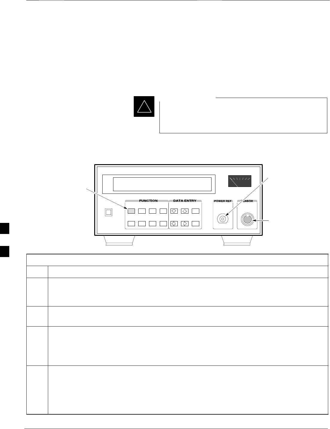
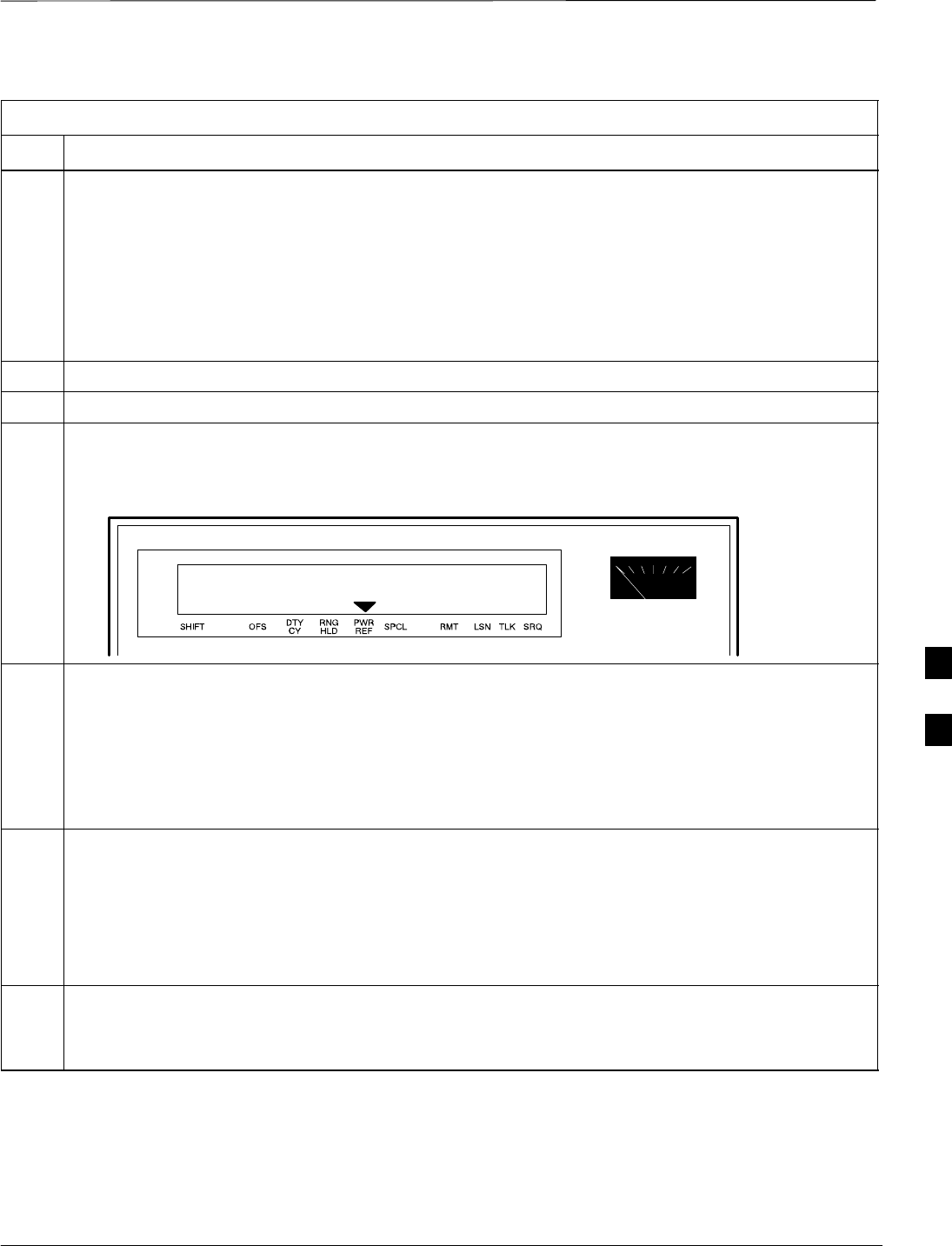
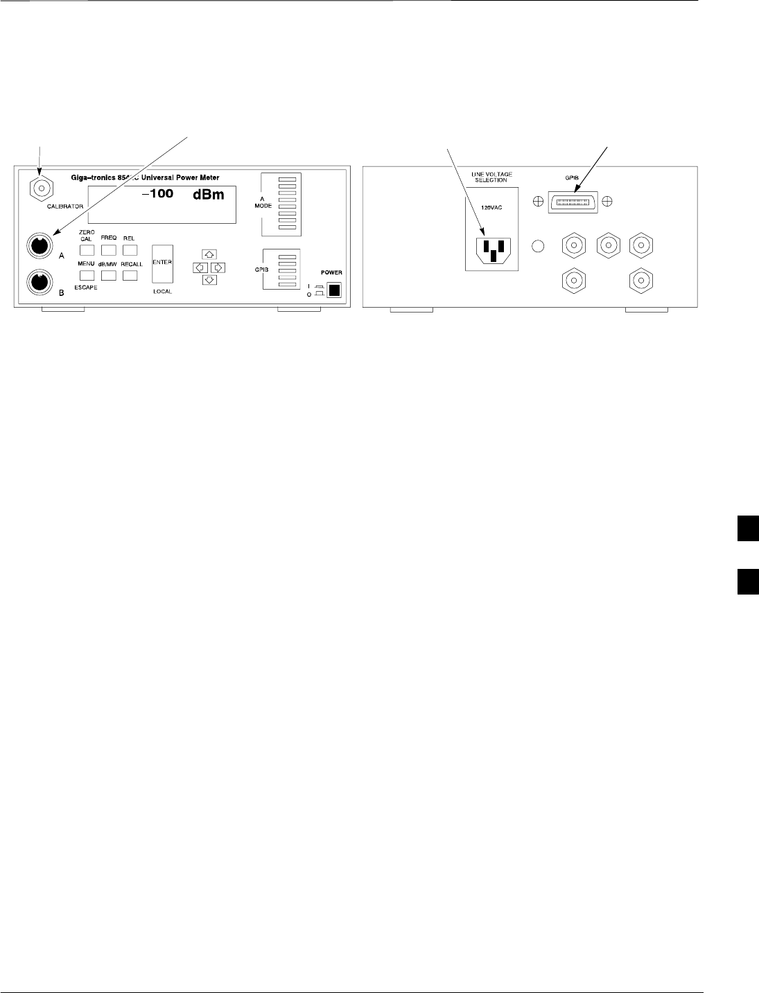
Calibrating Gigatronics 8541C
power meter
Precise transmit output power calibration measurements are made using
a bolometer–type broadband power meter with a sensitive power sensor.
Follow the steps in Table F-12 to enter information unique to the power
sensor.
Table F-12: Calibrate Gigatronics 8541C Power Meter
Step Action
! CAUTION
Do not connect/disconnect the power meter sensor cable with AC power applied to the meter.
Disconnection could result in destruction of the sensing element or miscalibration.
NOTE
Allow the power meter and sensor to warm up and stabilize for a minimum of 60 minutes before
performing the calibration procedure.
1SMake sure the power meter POWER pushbutton is OFF.
SConnect the power sensor cable to the SENSOR input.
SSet the POWER pushbutton to ON.
2Verify the Power GPIB mode and address:
SPress MENU. Use the b arrow key to select CONFIG MENU, and press ENTER.
SUse the b arrow key to select GPIB, and press ENTER.
SUse the by arrow keys to set MODE to 8541C.
SPress ' and use the by arrow keys as required to set ADDRESS to 13.
SPress ENTER.
3SConnect the power sensor to the CALIBRATOR output connector.
SPress ZERO.
SWait for the process to complete. Sensor factory calibration data is read to power meter during this
process.
SDisconnect the power sensor from the CALIBRATOR output.
F
Manual Cable Calibration – continued
Jan 2002 F-21
SCt4812ET BTS Optimization/ATP — CDMA LMF
Figure F-9: Gigatronics 8541C Power Meter Detail
CONNECT POWER SENSOR
WITH POWER METER
TURNED OFF
CONNECT POWER SENSOR TO
CALIBRATOR POWER REFERENCE
WHEN CALIBRATING/ZEROING UNIT
FRONT View REAR View
GPIB CONNECTIONAC POWER
FW00564
F

Manual Cable Calibration – continued
SCt4812ET BTS Optimization/ATP — CDMA LMF Jan 2002
F-22
Notes
F

Jan 2002 SCt4812ET BTS Optimization/ATP — CDMA LMF
Appendix G: In–Service Calibration
Appendix Content
Introduction G-1. . . . . . . . . . . . . . . . . . . . . . . . . . . . . . . . . . . . . . . . . . . . . . . . . . . . .
Purpose G-1. . . . . . . . . . . . . . . . . . . . . . . . . . . . . . . . . . . . . . . . . . . . . . . . .
Equipment Warm up G-1. . . . . . . . . . . . . . . . . . . . . . . . . . . . . . . . . . . . . . .
Power Delta Calibration G-2. . . . . . . . . . . . . . . . . . . . . . . . . . . . . . . . . . . . . . . . . . .
Power Delta Calibration Introduction G-2. . . . . . . . . . . . . . . . . . . . . . . . . .
HP8921A Power Delta Calibration G-2. . . . . . . . . . . . . . . . . . . . . . . . . . . .
Advantest R3465 Power Delta Calibration G-4. . . . . . . . . . . . . . . . . . . . . .
HP8935 Power Delta Calibration G-7. . . . . . . . . . . . . . . . . . . . . . . . . . . . .
Agilent E4406A Power Delta Calibration G-9. . . . . . . . . . . . . . . . . . . . . . .
In–Service Calibration G-12. . . . . . . . . . . . . . . . . . . . . . . . . . . . . . . . . . . . . . . . . . . .
G

Table of Contents – continued
SCt4812ET BTS Optimization/ATP — CDMA LMF Jan 2002
Notes
G
Introduction
Jan 2002 G-1
SCt4812ET BTS Optimization/ATP — CDMA LMF
Purpose
This procedure is a guide to expanding your system with multiple
carriers while the system remains in service. This procedure also allows
you to perform on site maintenance (replace defective boards and
recalibrate) while the remainder of the site stays in service.
Motorola recommends that you perform this procedure during a
maintenance window.
This procedure cannot be performed on BTSs with 4–to–1 combiners.
The procedure can only be performed on one side of the BTS at one
time. That is, LPAs 1, 2 ,3, 7, 8, 9 (feed antennas 1, 2, 3) can be
calibrated while LPAs 6, 7, 8, 10, 11, 12 (feed antennas 4, 5, 6) remain
in service and vice versa.
Equipment Warm up
Calibration of the communications test set (or equivalent
test equipment) must be performed at the site before
calibrating the overall test set. Calibrate the test equipment
after it has been allowed to warm-up and stabilize for a
minimum of 60 minutes.
IMPORTANT
*
If any piece of test equipment (i.e., test cable, RF adapter)
has been replaced, re-calibration must be performed.
Failure to do so could introduce measurement errors,
causing incorrect measurements and degradation to system
performance.
CAUTION
G
Power Delta Calibration
SCt4812ET BTS Optimization/ATP — CDMA LMF Jan 2002
G-2
Power Delta Calibration
Introduction
The In–service calibration procedure has several differences from a
normal calibration procedure. One of these is the use of a spectrum
analyzer instead of a power meter to measure power. Power meters are
broadband measurement devices and cannot be used to measure power
during In–service Calibration since other carriers are operating. A
spectrum analyzer can be used because it measures power at a given
frequency. However, measuring power using a spectrum analyzer is less
accurate than using a power meter. Therefore, you must compensate for
the difference (delta) between the power meter and the spectrum
analyzer.
HP8921A Power Delta
Calibration
Use the HP8921A Spectrum Analyzer to measure power during
In–Service Calibration for 800 MHz systems. After the offset value has
been calculated, add it to the TX cable loss value.
Follow the procedure in Table G-1 to perform the HP8921A Power Delta
Calibration procedure.
This procedure requires two HP8921As.
NOTE
Table G-1: HP8921A Power Delta Calibration Procedure
Step Action
* IMPORTANT
Perform this procedure after test equipment has been allowed to warm–up and stabilize for a minimum
of 60 minutes.
1Connect a short RF cable between the HP8921A Duplex Out port and the HP437B power sensor (see
Figure G-1).
2Set the HP8921A signal source as follows:
–Measure mode to CDMA Generator
–Frequency to the CDMA Calibration target frequency
–CW RF Path to IQ
–Output Port to Dupl
–Data Source to Random
–Amplitude to 0 dBm
3Measure and record the power value reading on the HP437B Power Meter.
4Record the Power Meter reading as result A ________________________.
. . . continued on next page
G

Power Delta Calibration – continued
Jan 2002 G-3
SCt4812ET BTS Optimization/ATP — CDMA LMF
Table G-1: HP8921A Power Delta Calibration Procedure
Step Action
5Turn off the source HP8921A signal output, and disconnect the HP437B.
NOTE
Leave the settings on the source HP8921A for convenience in the following steps.
6Connect the short RF cable between the source HP8921A Duplex Out port and the measuring
HP8921A RF–IN port (see Figure G-2).
7Ensure that the source HP8921A settings are the same as in Step 2.
8Set the measuring HP8921A as follows:
–Measure mode to CDMA Anl
–Frequency to the CDMA calibration target frequency
–Input Attenuation to 0 dB
–Input port to RF–IN
–Gain to Auto
–Analyzer Direction to Fwd
9Turn on the source HP8921A signal output.
10 Measure and record the channel power reading on the measuring HP8921A as result
B ________________________.
11 Turn off the source HP8921A signal output and disconnect the equipment.
12 Compute the delta between HP437B and HP8921A using the following formula:
Delta = A – B
Example: Delta = –0.70 dBm – (–1.25 dBm) = 0.55 dBm
Example: Delta = 0.26 dBm – 0.55 dBm = –0.29 dBm
These examples are included to show the mathematics and do not represent actual readings.
NOTE
Add this delta value to the TX Cable Loss value during In–Service Calibration.
G
Power Delta Calibration – continued
SCt4812ET BTS Optimization/ATP — CDMA LMF Jan 2002
G-4
Figure G-1: Delta Calibration Setup – HP8921A to HP437B
Short RF Cable
HP 8921A
DUPLEX
OUT
HP437B
Power
Sensor
SENSOR
FW00801
Figure G-2: Delta Calibration Setup – HP8921A to
HP8921A Measurement HP8921A Source HP8921A
Short RF Cable
DUPLEX
OUT
RF
IN/OUT
FW00802
Advantest R3465 Power Delta
Calibration
Follow the procedure in Table G-2 to perform the Advantest 3465 Power
Delta Calibration procedure.
Table G-2: Advantest Power Delta Calibration Procedure
Step Action
* IMPORTANT
Perform this procedure after test equipment has been allowed to warm–up and stabilize for a minimum
of 60 minutes.
On the Advantest R3465:
1Press the SHIFT and the PRESET keys located below the CRT display.
2Press the ADVANCE key in the Measurement area of the control panel.
3Press the CDMA Sig CRT menu key.
4Press the FREQ key in the Entry area of the control panel.
. . . continued on next page
G

Power Delta Calibration – continued
Jan 2002 G-5
SCt4812ET BTS Optimization/ATP — CDMA LMF
Table G-2: Advantest Power Delta Calibration Procedure
Step Action
5Set the frequency to the desired value using the keypad entry keys.
6Press the LEVEL key in the Entry area of the control panel.
7Set the LEVEL to 0 dBm using the keypad entry keys.
8Verify the Mod CRT menu key is highlighting OFF, if not press the Mod key to toggle it OFF.
9Verify the Output CRT menu key is highlighting OFF, if not press the Output key to toggle it OFF.
On the HP 437 Power Meter:
10 Zero the Power Meter prior to connecting the power sensor to the RF cable from the signal generator.
* IMPORTANT
For best accuracy, always re–zero the power meter before connecting the power sensor to the
component being calibrated.
11 Connect the RF cable from the R3561L CDMA Test Source Unit RF OUT port to the power sensor,
refer to Figure G-3.
12 Press the Output CRT menu key to toggle the Output to ON.
13 Record the Power Meter reading as result A ________________________.
14 Press the Output CRT menu key to toggle the Output to OFF.
15 Connect the RF cable from the R3561L CDMA Test Source Unit RF OUT port to the Spectrum
Analyzer INPUT Port, refer to Figure G-4.
16 Press the Output CRT menu key to change the Output to ON.
17 Press the CW key in the Measurement area of the control panel.
18 Press the LEVEL key in the Entry area of the control panel.
19 Set the REF LEVEL to 10 dBm using the keypad entry keys.
20 Press the dB/div CRT menu key.
21 Press the 10 dB/div CRT menu key.
22 Press the FREQ key in Entry area of the control panel.
23 Set the frequency to the desired value using the keypad entry keys.
24 Press the more 1/2 CRT menu key.
25 Press the Preselector CRT menu key to highlight 3.0G.
26 Press the FORMAT key in the Display Control area of the control panel.
27 Press the TRACE CRT menu key.
28 Press the AVG A CRT menu key.
29 Set AVG to 20 using keypad entry keys.
. . . continued on next page
G
Power Delta Calibration – continued
SCt4812ET BTS Optimization/ATP — CDMA LMF Jan 2002
G-6
Table G-2: Advantest Power Delta Calibration Procedure
Step Action
30 Press the return CRT menu key.
31 Press the SPAN key in the Entry area of the control panel.
32 Press the Zero Span CRT menu key.
33 Press the BW key in the Entry area of the control panel.
34 Press the RBW CRT menu key to highlight MNL. using keypad entry keys enter 30 kHz.
35 Set RBW to 30 kHz using keypad entry keys.
36 Press the VBW CRT menu key to highlight MNL.
37 Set VBW to 1 MHz using keypad entry keys.
38 Press the Marker ON key in the Display Control area of the control panel.
39 Record the Marker Level reading as result B ________________________.
40 Calculate the Power Calibration Delta value. The delta value is the power meter measurement minus
the Advantest measurement.
Delta = A – B
Example: Delta = –0.70 dBm – (–1.25 dBm) = 0.55 dBm
Example: Delta = 0.26 dBm – 0.55 dBm = –0.29 dBm
These examples are included to show the mathematics and do not represent actual readings.
NOTE
Add this delta value to the TX Cable Loss value during In–Service Calibration.
Figure G-3: Delta Calibration Setup – R3561L to HP437B
Advantest Power
Sensor
RF OUT
Short RF Cable
HP437B
SENSOR
R3561L
FW00803
G
Power Delta Calibration – continued
Jan 2002 G-7
SCt4812ET BTS Optimization/ATP — CDMA LMF
Figure G-4: Delta Calibration Setup – R3561L to R3465
R3561L
RF OUT
INPUT
Short RF Cable
R3465
FW00804
HP8935 Power Delta
Calibration
Follow the procedure in Table G-3 to perform the HP8935 Power Delta
Calibration procedure.
Table G-3: HP8935 Power Delta Calibration Procedure
Step Action
* IMPORTANT
Perform this procedure after test equipment has been allowed to warm–up and stabilize for a minimum
of 60 minutes.
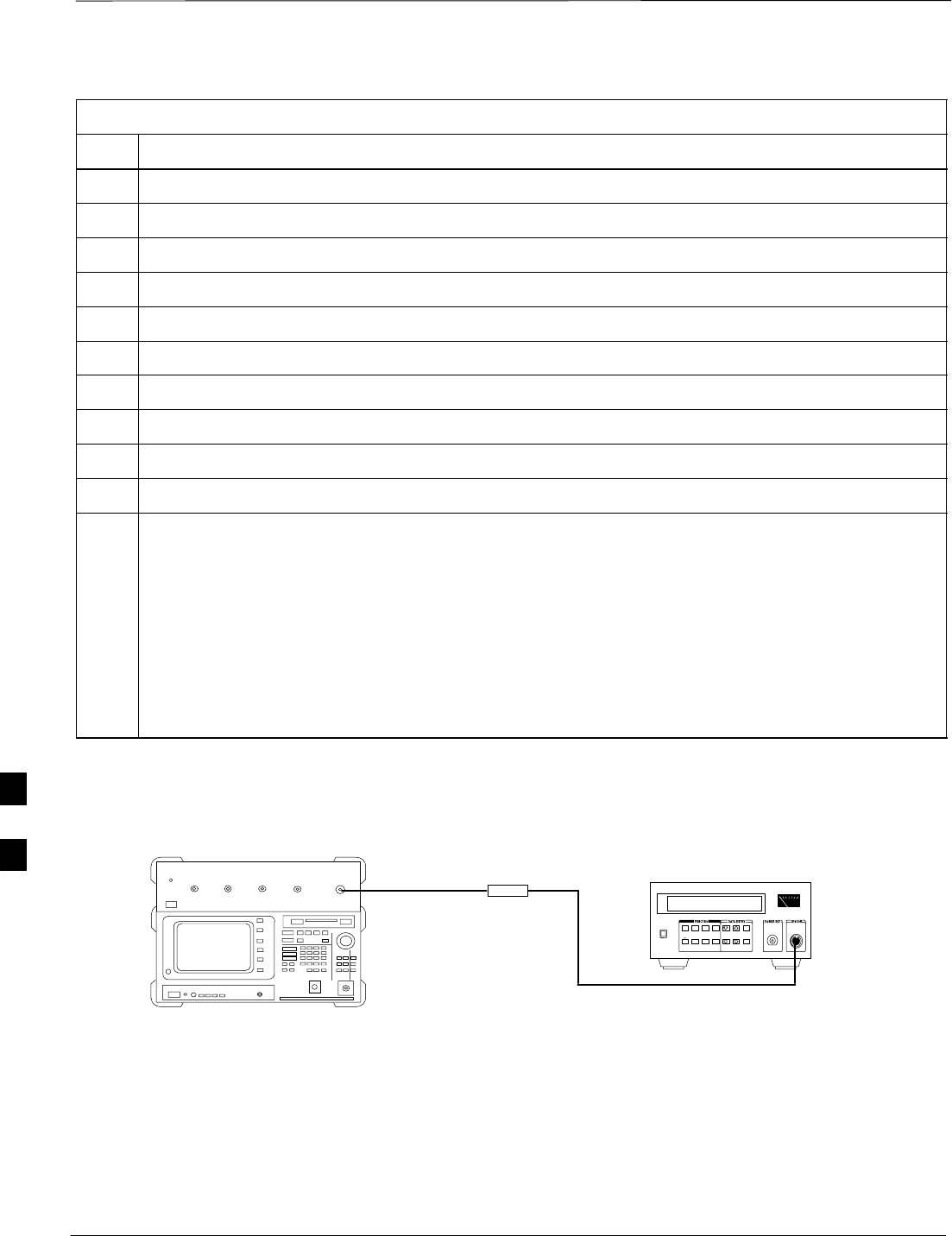
1Connect a short RF cable between the HP8935 Duplex Out port and the HP437B power sensor (see
Figure G-5).
2Set the HP8935 signal source as follows:
–Measure mode to CDMA Gen
–Frequency to the CDMA Calibration target frequency
–CW RF Path to IQ
–Output Port to Dupl
–Data Source to Random
–Amplitude to 0 dBm
3Measure and record the power value reading on the HP437B Power Meter.
4Record the Power Meter reading as result A ________________________.
5Turn off the source HP8935 signal output, and disconnect the HP437B.
NOTE
Leave the settings on the source HP8935 for convenience in the following steps.
6Connect the short RF cable between the source HP8935 Duplex Out port and the RF–IN/OUT port
(see Figure G-6).
7Ensure that the source HP8935 settings are the same as in Step 2.
. . . continued on next page
G
Power Delta Calibration – continued
SCt4812ET BTS Optimization/ATP — CDMA LMF Jan 2002
G-8
Table G-3: HP8935 Power Delta Calibration Procedure
Step Action
8Set the measuring HP8935 as follows:
–Measure mode to CDMA Anl
–Frequency to the CDMA calibration target frequency
–Input Attenuation to 0 dB
–Input port to RF–IN
–Gain to Auto
–Anl Dir to Fwd
9Turn on the source HP8935 signal output.
10 Set the Chn Pwr Cal to Calibrate and select to calibrate.
11 Measure and record the channel power reading on the measuring HP8935 as result
B ________________________.
12 Turn off the source HP8935 signal output and disconnect the equipment.
13 Calculate the Power Calibration Delta value. The delta value is the power meter measurement minus
the Advantest measurement.
Delta = A – B
Example: Delta = –0.70 dBm – (–1.25 dBm) = 0.55 dBm
Example: Delta = 0.26 dBm – 0.55 dBm = –0.29 dBm
These examples are included to show the mathematics and do not represent actual readings.
NOTE
Add this delta value to the TX Cable Loss value during In–Service Calibration.
Figure G-5: Delta Calibration Setup – HP8935 to HP437B
Power
Sensor
Hewlett–Packard Model HP 8935
DUPLEX OUT
Short RF Cable
HP437B
SENSOR
FW00805
G
Power Delta Calibration – continued
Jan 2002 G-9
SCt4812ET BTS Optimization/ATP — CDMA LMF
Figure G-6: Delta Calibration Setup – HP8935 to HP8935
Hewlett–Packard Model HP 8935
Short RF Cable
DUPLEX OUT RF IN/OUT
FW00806
Agilent E4406A Power Delta
Calibration
The Agilent E4406A transmitter tester and E4432B signal generator test
equipment combination can be used for CDMA 2000 as well as
IS–95A/B operation modes. The power delta calibration is performed on
the E4406A, but the E4432B is required to generate the reference signal
used to calculate the power delta offset. After the offset value has been
calculated, add it to the TX cable loss value in the LMF.
Follow the procedure in Table G-4 to perform the Agilent E4406A
Power Delta Calibration procedure.
Table G-4: Agilent E4406A Power Delta Calibration Procedure
Step Action
* IMPORTANT
Perform this procedure after test equipment has been allowed to warm–up and stabilize for a minimum
of 60 minutes. After it is warmed up and stabilized, calibrate the test equipment as described in the
“Test Set Calibration” section of the Optimization/Calibration chapter in the SC 4812ET
Optimization/ATP manual.
1Zero the Power Meter prior to connecting the power sensor to the RF cable from the signal generator.
* IMPORTANT
For best accuracy, always re–zero the power meter before connecting the power sensor to the
component being calibrated.
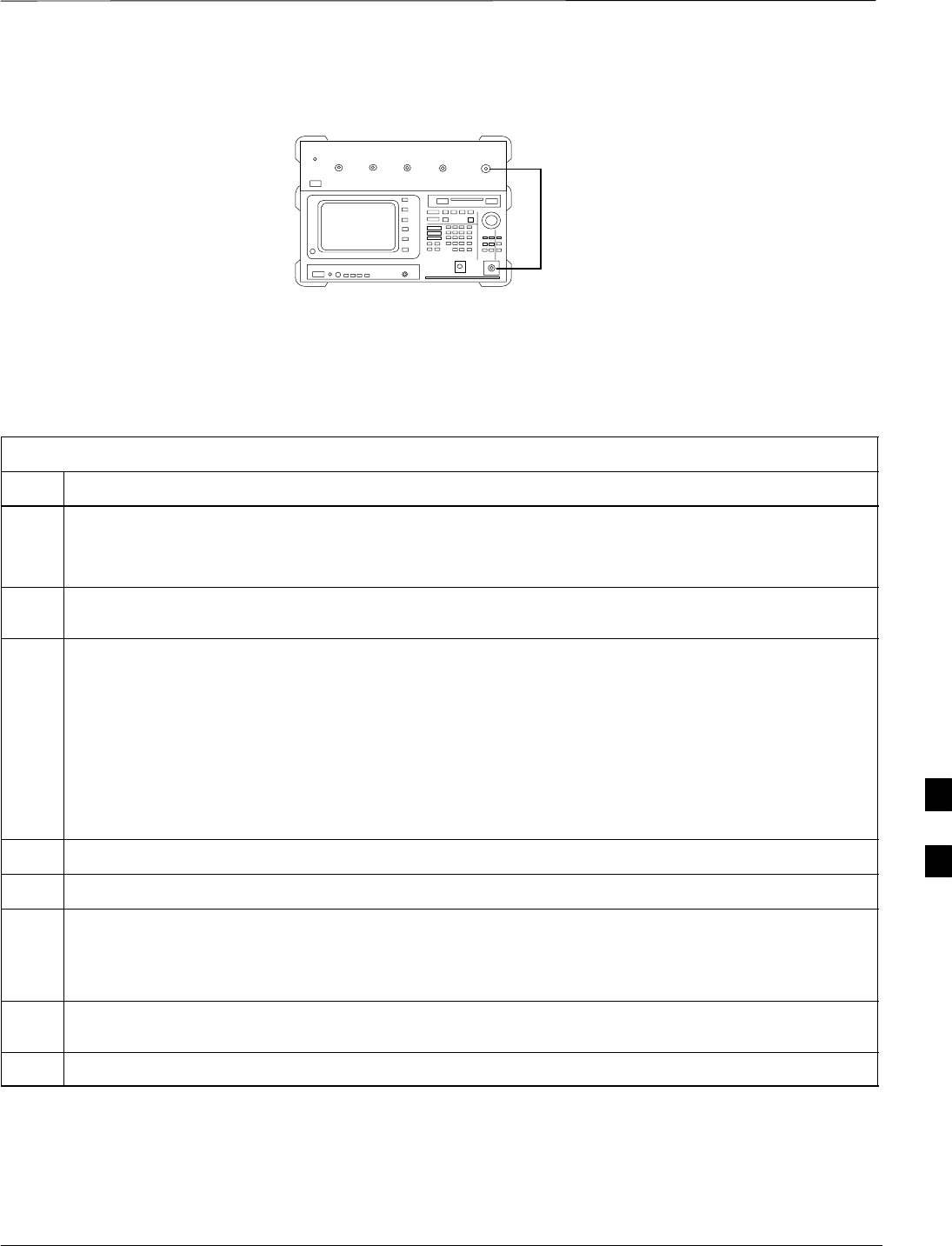
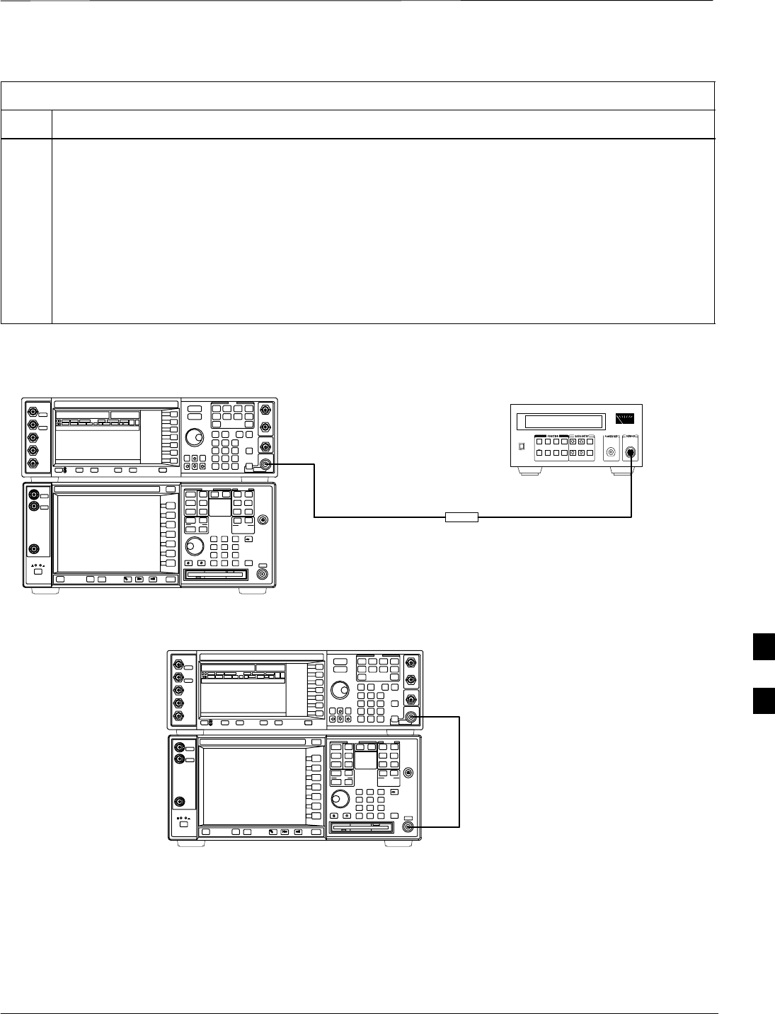
2Connect a short RF cable from the E4432B RF OUTPUT connector the HP437 power meter power
sensor (see Figure G-7).
3Set the E4432B signal generator as follows:
–Press Preset to exit any modes for which the signal generator is configured.
–Press Frequency and enter the frequency of the channel to be calibrated on the numeric keypad.
–Using the soft keys to the right of the screen, select the frequency range to be measured; for
example MHz.
–Press Amplitude and, using the numeric keypad, set signal amplitude to 0 (zero).
–Using the soft keys, set the measurement type to dBm.
. . . continued on next page
G

Power Delta Calibration – continued
SCt4812ET BTS Optimization/ATP — CDMA LMF Jan 2002
G-10
Table G-4: Agilent E4406A Power Delta Calibration Procedure
Step Action
4On the E4432B, press RF On/Off to toggle the RF output to RF ON.
–Note that the RF On/Off status in the screen display changes.
5Measure and record the value reading on the HP437 power meter as result A____________________.
6On the E4432B, press RF On/Off to toggle the RF output to RF OFF.
–Note that the RF On/Off status in the screen display changes.
7Disconnect the short RF cable from the HP437 power meter power sensor, and connect it to the RF
INPUT connector on the E4406A transmitter tester (see Figure G-8).
8* IMPORTANT
Do not change the frequency and amplitude settings on the E4432B when performing the following
steps.
Set the E4406A as follows:
–Press Preset to exit any modes for which the transmitter tester is configured
–Press MODE and, using the soft keys to the right of the screen, select cdmaOne
–Press MEASURE and, using the soft keys, select spectrum
–Press Frequency and, using the soft keys, select Center Frequency
–Enter the frequency of the channel to be calibrated using the numeric keypad
–Using the soft keys, select the frequency range to be measured; for example, MHz
–Press Input/Output and, using the soft keys, select Input Atten
–Using the numeric keypad, set Input Atten to 0 (zero) and, using the soft keys, select dB
–Using the soft keys, select External Atten and then select Mobile
–Using the numeric keypad, set Mobile to 0 (zero) and, using the soft keys, select dB
–Using the soft keys, select Base
–Using the numeric keypad, set Base to 0 (zero) and, using the soft keys, select dB
–Press MEASURE and, using the soft keys, select Channel Power
9On the E4432B signal generator, press RF On/Off to toggle the RF output to RF ON.
–Note that the RF On/Off status in the screen display changes.
10 Read the measured Channel Power from the E4406A screen display and record it as
result B____________________.
11 On the E4432B, press RF On/Off to toggle the RF output to RF OFF.
–Note that the RF On/Off status in the screen display changes.
. . . continued on next page
G
Power Delta Calibration – continued
Jan 2002 G-11
SCt4812ET BTS Optimization/ATP — CDMA LMF
Table G-4: Agilent E4406A Power Delta Calibration Procedure
Step Action
12 Calculate the Power Calibration Delta value. The delta value is the power meter measurement minus
the Agilent measurement.
Delta = A – B
Example: Delta = –0.70 dBm – (–1.25 dBm) = 0.55 dBm
Example: Delta = 0.26 dBm – 0.55 dBm = –0.29 dBm
These examples are included to show the mathematics and do not represent actual readings.
NOTE
Add this delta value to the TX Cable Loss value during In–Service Calibration.
Figure G-7: Delta Calibration Setup – Agilent E4432B to HP437
Power
Sensor
AGILENT E4432B AND E4406A
Short RF Cable
HP437B
SENSOR
RF OUTPUT
FW00858
Figure G-8: Delta Calibration Setup – Agilent E4432B to Agilent E4406A
Short RF
Cable
RF INPUT
AGILENT E4432B AND E4406A
RF OUTPUT
FW00859
G
In–Service Calibration
SCt4812ET BTS Optimization/ATP — CDMA LMF Jan 2002
G-12
In–Service Calibration
This feature does NOT have fault tolerance at this time.
The system has no safe–guards to stop you from doing
something that will take the BTS out of service. If
possible, perform this procedure during a maintenance
window.
Follow the procedures in this section precisely, otherwise
the entire BTS will most likely go OUT OF SERVICE.
At the CBSC, only perform operations on expansion
hardware when it is in the OOS_MANUAL state.
The operator must be trained in the LMF operation prior to
performing this procedure.
IMPORTANT
*
Prerequisites
SExpansion hardware has been added in the CBSC database, and the
CDF file has been generated.
SThe expansion devices have been inserted into the C–CCP cage and
are in the OOS_MANUAL state at the CBSC.
SThe site specific cdf (with the expansion hardware) and cal files have
been loaded onto the LMF.
SThe LMF has the same code and dds files as the CBSC to download.
Do not download code or data to any cards other than those
you are working on. Downloading code or data to other
cards will take the site OUT OF SERVICE.
The code file version numbers must match the version
numbers on the other cards in the frame. If the numbers do
not match, the site may go OUT OF SERVICE.
The BTS–#.cdf, CBSC–#.cdf, and CAL files for this BTS
must have come from the CBSC.
IMPORTANT
*
STest equipment has been configured per Figure G-9 or Figure G-10.
SAn RFDS (or at a minimum a directional coupler), whose loss is
already known, must be in line to perform the in–service calibration.
STest equipment has been calibrated after 1 hour warm up.
SA short RF cable and two BNC–N adapters are available to perform
Cable Calibration.
. . . continued on next page
G
In–Service Calibration – continued
Jan 2002 G-13
SCt4812ET BTS Optimization/ATP — CDMA LMF
SThe Power Delta Calibration has been performed (see Table G-1,
Table G-2, or Table G-3).
TX
TEST
CABLE
Hewlett–Packard Model HP 8935
DUPLEX OUT
TEST SETS Optimization/ATP SET UP
RF IN/OUT
HP–IB
TO GPIB
BOX
RX ANTENNA
PORT TX ANTENNA
PORT
RS232–GPIB
INTERFACE BOX
INTERNAL PCMCIA
ETHERNET CARD
GPIB
CABLE
UNIVERSAL TWISTED
PAIR (UTP) CABLE
(RJ45 CONNECTORS)
RS232 NULL
MODEM
CABLE
S MODE
DATA FORMAT
BAUD RATE
GPIB ADRS G MODE
ON
BTS
TX
TEST
CABLE
CDMA
LMF
DIP SWITCH SETTINGS
10BASET/
10BASE2
CONVERTER
LAN
B
LAN
A
RX
TEST
CABLE
COMMUNICATIONS
TEST SET
IEEE 488
GPIB BUS
RF IN/OUT
NOTE: IF BTS RX/TX SIGNALS ARE
DUPLEXED: BOTH THE TX AND RX TEST
CABLES CONNECT TO THE DUPLEXED
ANTENNA GROUP.
ANTENNA
RFDS
DUPLEXER
DIRECTIONAL
COUPLER
EVEN
SECOND/
SYNC IN
EXT
REF
IN
FREQ
MONITOR
SYNC
MONITOR
CSM
REF FW00759
SYNC MONITOR
EVEN SEC TICK
PULSE REFERENCE
FROM CSM BOARD
FREQ MONITOR
19.6608 MHZ CLOCK
REFERENCE FROM
CSM BOARD
RX
TEST
CABLE
FWD
COUPLED
PORT
Figure G-9: Optimization/ATP Test Setup Using RFDS
20 DB PAD
(FOR 1.7/1.9 GHZ)
10 DB PAD
(FOR 800 MHZ)
20 DB PAD
(FOR 1.7/1.9 GHZ)
10 DB PAD
(FOR 800 MHZ)
DUPLEX
OUT
G
In–Service Calibration – continued
SCt4812ET BTS Optimization/ATP — CDMA LMF Jan 2002
G-14
TEST SETS Optimization/ATP SET UP
Figure G-10: IS–95 A/B/C Optimization/ATP Test Setup Using RFDS
RF
INPUT 50
OHMS
RF
OUT 50
OHMS
Agilent E4432B (Top) and E4406A (Bottom)
FREQ MONITOR
19.6608 MHZ CLOCK
REFERENCE FROM
CSM BOARD
SYNC MONITOR
EVEN SEC TICK
PULSE REFERENCE
FROM CSM BOARD
BNC
“T”
TO TRIGGER IN
ON REAR OF
TRANSMITTER
TESTER
TO PATTERN TRIG IN
ON REAR OF SIGNAL
GENERATOR
TO 10 MHZ IN
(EXT REF IN)
ON REAR OF
TRANSMITTER
TESTER
INPUT 50
OHM
RF OUT
50 OHM
Advantest R3267 (Top) and R3562 (Bottom)
FREQ MONITOR
19.6608 MHZ CLOCK
REFERENCE FROM
CSM BOARD
SYNC MONITOR
EVEN SEC TICK
PULSE REFERENCE
FROM CSM BOARD
BNC
“T”
NOTE:
SYNTHE REF IN ON REAR OF SIGNAL GENERATOR IS
CONNECTED TO 10 MHZ OUT ON REAR OF SPECTRUM
ANALYZER
TO EXT TRIG
ON REAR OF
SPECTRUM
ANALYZER
TX
TEST
CABLE
RX ANTENNA
PORT TX ANTENNA
PORT
RS232–GPIB
INTERFACE BOX
INTERNAL PCMCIA
ETHERNET CARD
GPIB
CABLE
UNIVERSAL TWISTED
PAIR (UTP) CABLE
(RJ45 CONNECTORS)
RS232 NULL
MODEM
CABLE
S MODE
DATA FORMAT
BAUD RATE
GPIB ADRS G MODE
ON
BTS
TX
CABLE
CDMA
LMF
DIP SWITCH SETTINGS
10BASET/
10BASE2
CONVERTER
LAN
B
LAN
A
RX
TEST
CABLE
COMMUNICATIONS
TEST SET
IEEE 488
GPIB BUS
RF
INPUT
50
OHMS
RF OUT 50
OHMS
NOTE: IF BTS RX/TX SIGNALS ARE
DUPLEXED: BOTH THE TX AND RX TEST
CABLES CONNECT TO THE DUPLEXED
ANTENNA GROUP.
ANTENNA
RFDS
DUPLEXER
DIRECTIONAL
COUPLER
EVEN
SECOND/
SYNC IN
EXT
REF
IN
FREQ
MONITOR
SYNC
MONITOR
CSM
REF. FW00759
RX
CABLE
FWD
COUPLED
PORT
SIGNAL
GENERATOR
EXT TRIG IN
MOD TIME BASE IN
(EXT REF IN)
19.6608
MHZ
CLOCK
20 DB PAD
(FOR 1.7/1.9 GHZ)
10 DB PAD
(FOR 800 MHZ)
BNC
“T”
G

In–Service Calibration – continued
Jan 2002 G-15
SCt4812ET BTS Optimization/ATP — CDMA LMF
Follow the procedure in Table G-5 to perform the In–Service
Calibration.
Table G-5: In–Service Calibration
Step Action
* IMPORTANT
Perform this procedure after test equipment has been allowed to warm–up and stabilize for a minimum
of 60 minutes.
1Set up the LMF for In–Service Calibration:
–Start the LMF by double–clicking the LMF icon on the Windows desktop.
–Click Tools>Options from the menu bar at the login screen.
–Check the applicable spectrum analyzer check box and the signal generator check box on the Test
Equipment tab.
Ensure that the GPIB address is 18 for the CDMA analyzer and 1 for the signal generator.
–Uncheck any other other equipment that is selected.
–Click the Apply button.
–Select the BTS Options tab in the LMF Option window.
–Check the In–Service Calibration check box.
–Click the Apply button.
–Click the Dismiss button to close the LMF Option window.
2Login to the target BTS:
–Select the target BTS icon.
–Click the Login button at the login screen.
3Measure the Cable Loss using the Cable Calibration function:
–Click Util>Cable Calibration from the menu bar at the main window.
–Set the desired channel(s) and select TX and RX CABLE CAL at the cable calibration pop up
window.
–Click the OK button to perform cable calibration.
–Follow the on–screen instructions to complete the cable loss measurement.
NOTE
–The measured value is input automatically to the cable loss file.
–To view the cable loss file, click Util>Examine>Cable Loss>TX or RX.
. . . continued on next page
G

In–Service Calibration – continued
SCt4812ET BTS Optimization/ATP — CDMA LMF Jan 2002
G-16
Table G-5: In–Service Calibration
Step Action
4Add the spectrum analyzer power delta to the Cable Loss.
–To view the cable loss file, click Util>Examine>Cable Loss>TX or RX.
–Add the value computed in Table G-1, Table G-2, or Table G-3 to the TX Cable Loss.
NOTE
Be sure to include the sign of the value. The following examples are included to show the mathematics
and do not represent actual readings:
–Example: 5.65 dBm + 0.55 dBm = 6.20 dBm
–Example: 5.65 dBm + (–0.29 dBm) = 5.36 dBm
–Example: –5.65 dBm + 0.55 dBm = –5.10 dBm
–Example: –5.65 dBm + (–0.29 dBm) = –5.94 dBm
5Input the Coupler Loss for the TX and RX tests:
–Click Util>Edit>Coupler Loss>TX or RX from the menu bar at the main window.
–Input the appropriate coupler loss for the target carrier(s) by referring to the information taken at
the time of BTS installation.
–Click the Save button.
–Click the Dismiss button to close the window.
–To view the coupler loss file, click Util>Examine>Coupler Loss>TX or RX.
6Have the CBSC operator put the redundant BBX OOS_MANUAL.
! CAUTION
Be sure to download OOS devices only. Loading in–service devices takes them OUT OF SERVICE
and can result in dropped calls.
The code file version numbers must match the version numbers on the other cards in the frame. If the
numbers do not match, the site may go OUT OF SERVICE.
NOTE
Be sure to include the redundant BBX in steps 9, 10, and 11.
7Download code and data to the target devices:
–Click Tools>Update NextLoad>CDMA to set the code version that will be downloaded.
–Select the BTS(s) you need, check the appropriate code version in the pop up window, and click
the Save button to close.
–Select the target BBX(s) on the C–CCP cage picture.
–Click Device>Download>Code/Data to start downloading code.
–Select the target BBX(s) on the C–CCP cage picture.
–Click Device>Download>Data to start downloading data.
. . . continued on next page
G

In–Service Calibration – continued
Jan 2002 G-17
SCt4812ET BTS Optimization/ATP — CDMA LMF
Table G-5: In–Service Calibration
Step Action
! CAUTION
Perform the In–service Calibration procedure on OOS devices only.
8Select the desired test:
–Select the target BBX(s) on the C–CCP cage picture.
–Click Tests>[desired test] from the menu bar at the main window.
–Select the target carrier and confirm the channel number in the pop up window.
–Leave the Verify BLO check box checked.
–From the Test Pattern pick list, select a test pattern.
–Click the OK button to start calibration.
–Follow the on–screen instructions, except, do not connect to the BTS antenna port, connect to the
directional coupler (fwd) port associated with the on screen prompt antenna port.
NOTE
SSelecting Pilot (default) performs tests using a pilot signal only.
SSelecting Standard performs tests using pilot, synch, paging and six traffic channels. This requires
an MCC to be selected.
SSelecting CDFPilot performs tests using the CDF value for pilot gain and IS–97 gain values for all
the other channels included in the Standard pattern setting (paging, synch, and six traffic). Using
this pattern setting requires the selection of both a BBX and at least one MCC.
SSelecting CDF performs tests using pilot, synch, paging and six traffic channels, however, the gain
for the channel elements is specified in the CDF file.
9Save the result and download the BLO data to the target BBX(s):
–Click the Save Result button on the result screen.
The window closes automatically.
10 Logout from the BTS and close the LMF session:
–Click BTS>Logout to close the BTS connection.
–Close the LMF window.
11 Restore the new “bts–*.cal” file to the CBSC.
12 Enable the target device(s) from the CBSC.
G

In–Service Calibration – continued
SCt4812ET BTS Optimization/ATP — CDMA LMF Jan 2002
G-18
Notes
G

Jan 2002 SCt4812ET BTS Optimization/ATP — CDMA LMF
Appendix H: RF Cabinet Interconnect Cables
Appendix Content
SC 4812ET Inter−Cabinet Cabeling HĆ1. . . . . . . . . . . . . . . . . . . . . . . .
C−CCP Cables and Cable Connectors HĆ4. . . . . . . . . . . . . . . . . . . . . .
RF Cabinet LPA Cables HĆ7. . . . . . . . . . . . . . . . . . . . . . . . . . . . . . . . . . .
LPAC Cabling HĆ11. . . . . . . . . . . . . . . . . . . . . . . . . . . . . . . . . . . . . . . . . . .
ETIB Cables and Cable Connectors HĆ12. . . . . . . . . . . . . . . . . . . . . . . . .
SPAN I/O Cable Connection Diagram HĆ13. . . . . . . . . . . . . . . . . . . . . . .
DRDC/TRDC Cables and Cable Connections HĆ15. . . . . . . . . . . . . . . .
MPC to DRDC Cabling HĆ20. . . . . . . . . . . . . . . . . . . . . . . . . . . . . . . . . . .
RFDS Cabling Details HĆ22. . . . . . . . . . . . . . . . . . . . . . . . . . . . . . . . . . . .
50 Pair Punchblock HĆ25. . . . . . . . . . . . . . . . . . . . . . . . . . . . . . . . . . . . . . .
H

Table of Contents – continued
SCt4812ET BTS Optimization/ATP — CDMA LMF Jan 2002
Notes
H
RF Cabinet Interconnect Cables
Jan 2002 H-1
SCt4812ET BTS Optimization/ATP — CDMA LMF
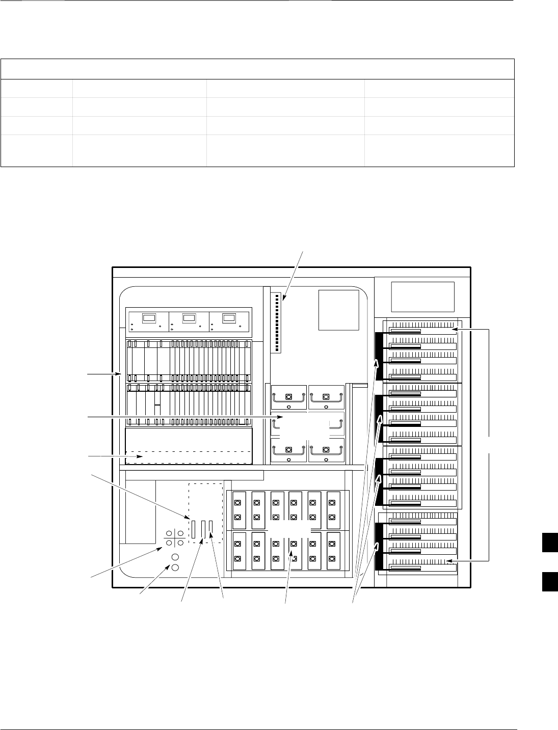
SC 4812ET Intra–Cabinet
Cabling
This appendix provides the identification and location of the cables
connecting the components which make up the SC 4812ET RF cabinet.
The number of cables and components incorporated in the RF cabinet
will vary depending on the the manner in which the cabinet is equipped.
For example, a 3 sector, 2 carrier system will require less components
and less cables than a 6 sector 2 carrier system.
Refer to Table H-1 and Figure H-1 through Figure H-19 for the cable
you wish to research.
In some cases cables with the same number are used to
connect two different signalling paths. These cables are
designated A & B and the point they connect to and from
is also designated A & B. Ensure the correct cable (A or B)
is connected to the correct designation (A or B) connector
or plug.
IMPORTANT
*
Table H-1 : 4812ET RF CABINET INTER–CONNECT CABLES
DRDC, Combiner, Trunking Backplane Cables
CABLE # FROM NOTE’sTO
3064795A05 TX CIO Figure H-6 Trunking BP
3064735A10 TX Trunking BP Figure H-5 Combiner Connector Pnl
3064735A07 TX Combiner See Figure H-1, Figure H-11,
Figure H-12, Figure H-13, and
Figure H-14
DRDC
3064735A11 TX Combiner (See Above) DRDC
3064735A12 TX Combiner (See Above) DRDC
3064795A07 TX CIO Figure H-11 Trunking BP
3086435H01 TX Combiner QDS PkZ Adptr
3086435H02 TX Combiner QDS PkZ Adptr
3086435H03 TX Combiner QDS PkZ Adptr
3086168H01 Power LPA PDA Figure H-5 Trunk BP
C–CCP Cables
CABLE # FROM NOTE’sTO
3064809A01 Power CCCP/PDA See Figure H-1 & Figure H-5 C–CCP Backplane
3064899A04 LAN I/O A in See Figure H-1 & Figure H-5 C–CCP LAN I/O A In
. . . continued on next page
H

RF Cabinet Interconnect Cables – continued
SCt4812ET BTS Optimization/ATP — CDMA LMF Jan 2002
H-2
Table H-1 : 4812ET RF CABINET INTER–CONNECT CABLES
C–CCP Cables (cont)
CABLE # FROM NOTEs TO
3064899A04 LAN I/O B in See Figure H-1 & Figure H-5 C–CCP LAN I/O B In
3086033H03 GPS Surge Arrestor See Figure H-1 & Figure H-5 C–CCPBackplane
3064899A04 LAN I/O B in See Figure H-1 & Figure H-5 C–CCP LAN I/O B In
3064899A03 C–CCP LAN I/O A Out See Figure H-1 & Figure H-5 LAN I/O A Out
3064899A03 C–CCP LAN I/O B Out See Figure H-1 & Figure H-5 LAN I/O B Out
3064899A07 Sync CSM See Figure H-1 I/O
3086000H02 Site I/O C–CCP See Figure H-9 J2 on ETIB
3086001H02 A SPAN I/O BlkHd See Figure H-1 & Figure H-5 C–CCP/A SPAN I/O
3086001H02 B SPAN I/O BlkHd See Figure H-1 & Figure H-5 C–CCP/B SPAN I/O
3086086H02 Alarm C–CCP See Figure H-1 & Figure H-9 J1 on ETIB
3086366H02 HSO/LFR See Figure H-1 & Figure H-5 C–CCP HSO/LFR
4886044H01 LBD See Figure H-1 & Figure H-5 C–CCP Backplane
Span I/O Board Cables
CABLE # FROM NOTEs TO
3086601H01 SPAN I/O Pblock See Figure H-1 & Figure H-10 CSU
3086601H02 SPAN CSU See Figure H-1 & Figure H-10 A & B SPAN I/O BRD
3086001H02 SPAN CSU See Figure H-1 & Figure H-10 A & B SPAN Connector on
C–CCP Backplane
RFDS Cables
CABLE # FROM NOTE’sTO
3064238A17 RFDS/ASU–1Figure H-16 & Figure H-17 DRDC
3064238A18 RFDS/ASU–2Figure H-16 & Figure H-17 DRDC
3064238A19 RFDS/ASU–1Figure H-16 & Figure H-17 DRDC
3064238A20 RFDS/ASU–2Figure H-16 & Figure H-17 DRDC
ETIB/LPAC Cables
CABLE # FROM NOTE’sTO
3064794A03 LPAC See Figure H-8 C–CCP Bkpln
3064794A05 ETIB See Figure H-9 & Figure H-16 RFDS
3086433H04 RGPS I/O See Figure H-1 & Figure H-9 ETIB (15 position)
3086169H01 Power, Heat Exchanger,
PDA See Figure H-1 & Figure H-9 ETIB, OPT, HX, EBA
3086500H01 Alm/Ctrl ETIB See Figure H-1 & Figure H-9 HX/LPA
. . . continued on next page
H
RF Cabinet Interconnect Cables – continued
Jan 2002 H-3
SCt4812ET BTS Optimization/ATP — CDMA LMF
Table H-1 : 4812ET RF CABINET INTER–CONNECT CABLES
3086505H01 DC Cable (DC Power Dist) See Figure H-1 & Figure H-19 EBA Blower Assembly
3086566H01 LPAC See Figure H-1 & Figure H-8 1 Cable to each LPA Bk Pln
3086569H01 Door Intrusion Alarm See Figure H-5 & Figure H-19 Door Switch
3086655H02 LPAC See Figure H-8, Figure H-5 &
Figure H-19 ETIB
Figure H-1: 4812ET RF Cabinet Internal FRU Locations
LPA’s
LPA Trunking
Backplane
RFDS
DC
Power
Dist.
Punch
Block
(back)
EBA
OPTIONAL AREA
Span I/O
Alarm to
ETIB
ETIB
LPAC
SPAN I/O
A
B
IN
OUT
LAN
19 MHz
2 Sec
CSU
(See Figure H-8,
Figure H-9), and
Figure H-10)
(See Figure H-4,
Figure H-5, Figure H-6
and Figure H-8)
DRDC
FW00698
SYS
Sync LPA Trunking
Backplane
RFDS
DC
Power
Dist.
Punch
Block
(back)
EBA
C–CCP Shelf
Combiner
Cage
OPTIONAL AREA
Span I/O
to C–CCP Alarm to
ETIB
ETIB
LPAC
SPAN I/O
A
B
IN
OUT
LAN
LAN I/O
19 MHz
2 Sec
CSU
(See Figure H-2
and Figure H-5)
(See Figure H-11,
Figure H-12,
Figure H-13, and
Figure H-14)
(See Figure H-11)
(See Figure H-10)
DRDC
FW00698
SYS
Sync
(See Figure H-5
and Figure H-10)
Modem
To
H

RF Cabinet Interconnect Cables – continued
SCt4812ET BTS Optimization/ATP — CDMA LMF Jan 2002
H-4
C–CCP Cables and Cable
Connectors
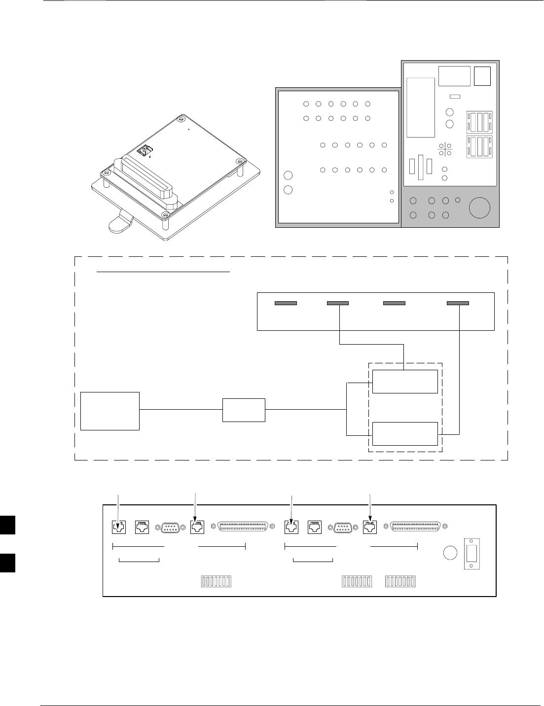
The C-CCP Shelf assembly consists of the C-CCP Shelf and the attached
backplane with cables and connectors (see Figure H-2 and Figure H-3).
The C–CCP shelf contains all of the CDMA unique functions within the
SC 4812ET RF frame. The C–CCP shelf contains the following
components:
SBroadband Transceiver (BBX) cards
SMulti–Channel CDMA (MCC) cards
SCombiner Input/Output (CIO) card
SPower Supply cards
SGroup Line Interface (GLI2) cards
SAlarm Monitor Reporting (AMR) cards
SClock Synchronization Modules (CSM)
SHigh Stability Oscillator/Low frequency Receiver (HSO/LFR)
SMulticoupler Preselector Cards (MPC)
SCDMA Clock Distribution (CCD) card
SIntegrated Frame Modem (IFM) card
SSwitch card
SC–CCP Fan Modules
H
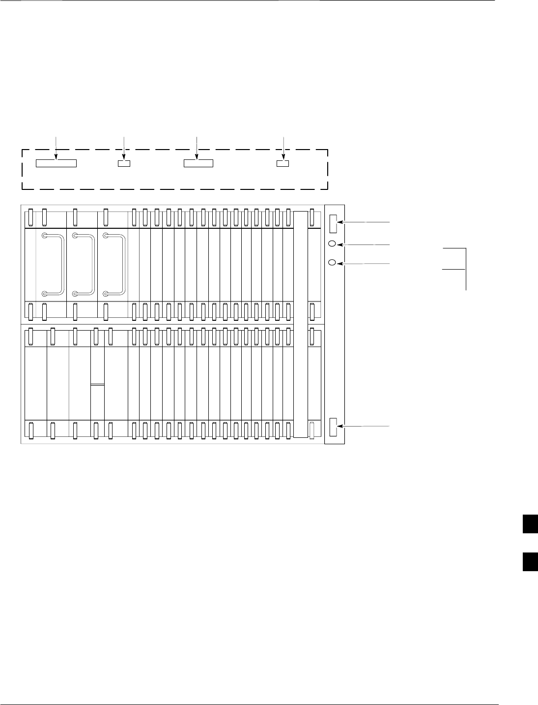
RF Cabinet Interconnect Cables – continued
Jan 2002 H-5
SCt4812ET BTS Optimization/ATP — CDMA LMF
Figure H-2: C-CCP Shelf Cable Numbers and Connectors
PS–3
AMR–1
HSO/LFR
CSM–1
CSM–2
FILLER
AMR–2
GLI2–1GLI2–2
MCC24–6
BBX2–1
BBX2–2
BBX2–3
BBX2–4
BBX2–5
BBX2–6
BBX2–13Switch Card
MPC/EMPC–1MPC/EMPC–2
CIO
BBX2–7
BBX2–8
BBX2–9
BBX2–10
BBX2–11
BBX2–12
MCC24–5
MCC24–4
MCC24–3
MCC24–2
MCC24–1
MCC24–12
MCC24–11
MCC24–10
MCC24–9
MCC24–8
MCC24–7
PS–2
PS–1
CCD–2 CCD–1
19 mm Filter Panel
C–CCP Shelf
SPAN A SPAN B
Cable #
3064794A03
Cable #
3086366H02
Cable #
3064899A04
Cable #
3064899A04
LPAC
ALARMS SITE I/O
HSO/LFR
LAN I/O A
LAN I/O B
Cable #
3086001H02
Cable #
3086000H02
Cable #
3086001H02
Cable #
3086086H02
To LAN I/O
connectors on
the Bulkhead
(To J1
connector on
the ETIB)
(To SPAN A I/O
connector on
the Bulkhead)
(To SPAN B I/O
connector on the
Bulkhead)
(To J2
connector on
the ETIB)
(To the C–CCP
connector on the
LPAC Module)
FW00699
H
RF Cabinet Interconnect Cables – continued
SCt4812ET BTS Optimization/ATP — CDMA LMF Jan 2002
H-6
SYSTEM
LED
LAN OUT B
GPS
Figure H-3: C–CCP Backplane
FW00700
Cable #
3064794A03
Cable #
3086366H02
Cable #
3064899A04
Cable #
3064899A04
LPAC
HSO/LFR
LAN IN A
LAN IN B
Cable #
3086001H02
Cable #
3086000H02
Cable #
3086001H02
Cable #
3086086H02
To LAN I/O
connectors on
the Bulkhead
(To J1
connector on
the ETIB)
(To SPAN A I/O
connector on
the Bulkhead)
(To SPAN B I/O
connector on the
Bulkhead)
(To J2
connector on
the ETIB)
(To the C–CCP
connector on the
LPAC Module)
CCCP Power
3064809A01
LAN OUT A Cable #
3064899A03
Cable #
3064899A03
Cable #
3086033H03
Cable #
4886044H01
H
RF Cabinet Interconnect Cables – continued
Jan 2002 H-7
SCt4812ET BTS Optimization/ATP — CDMA LMF
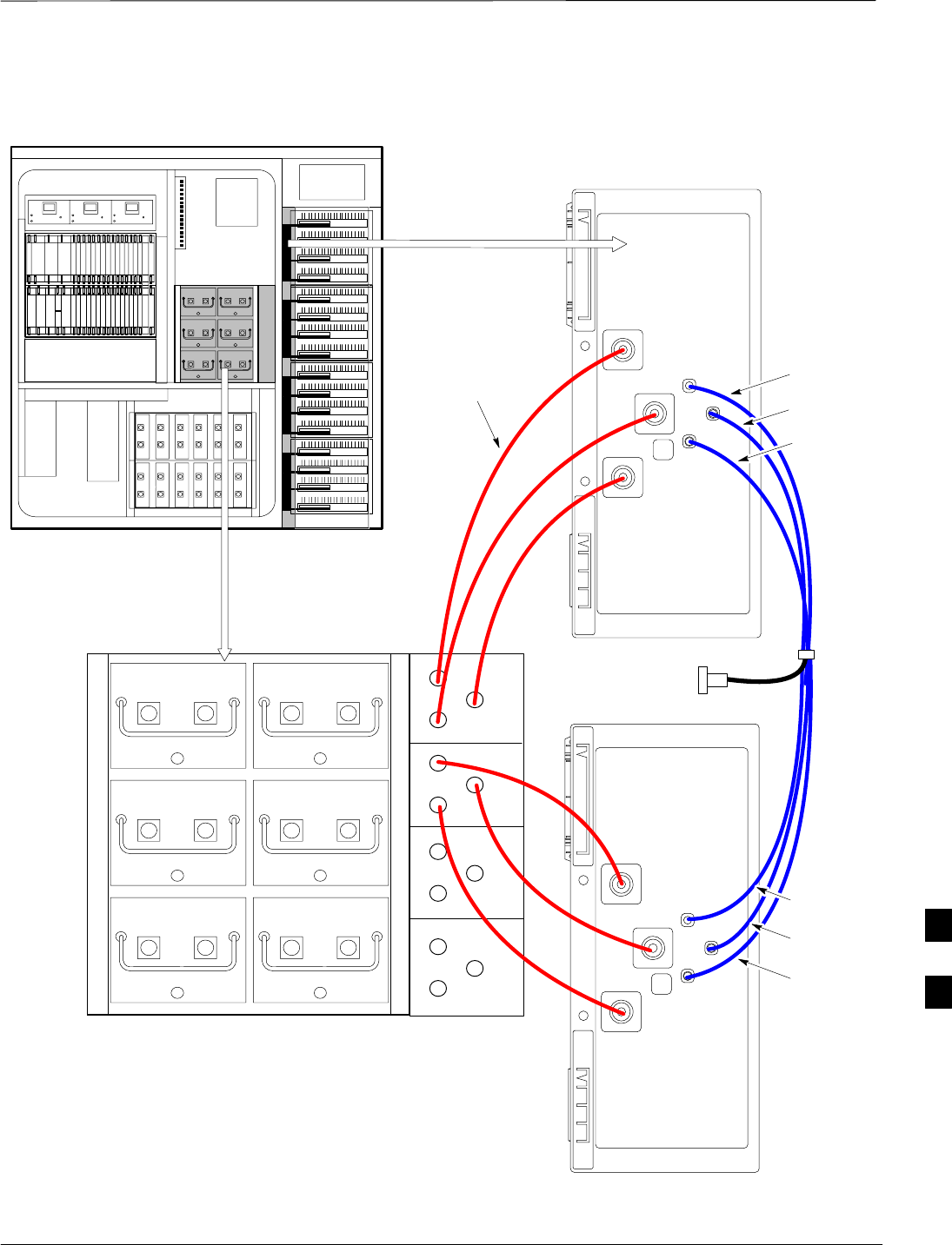
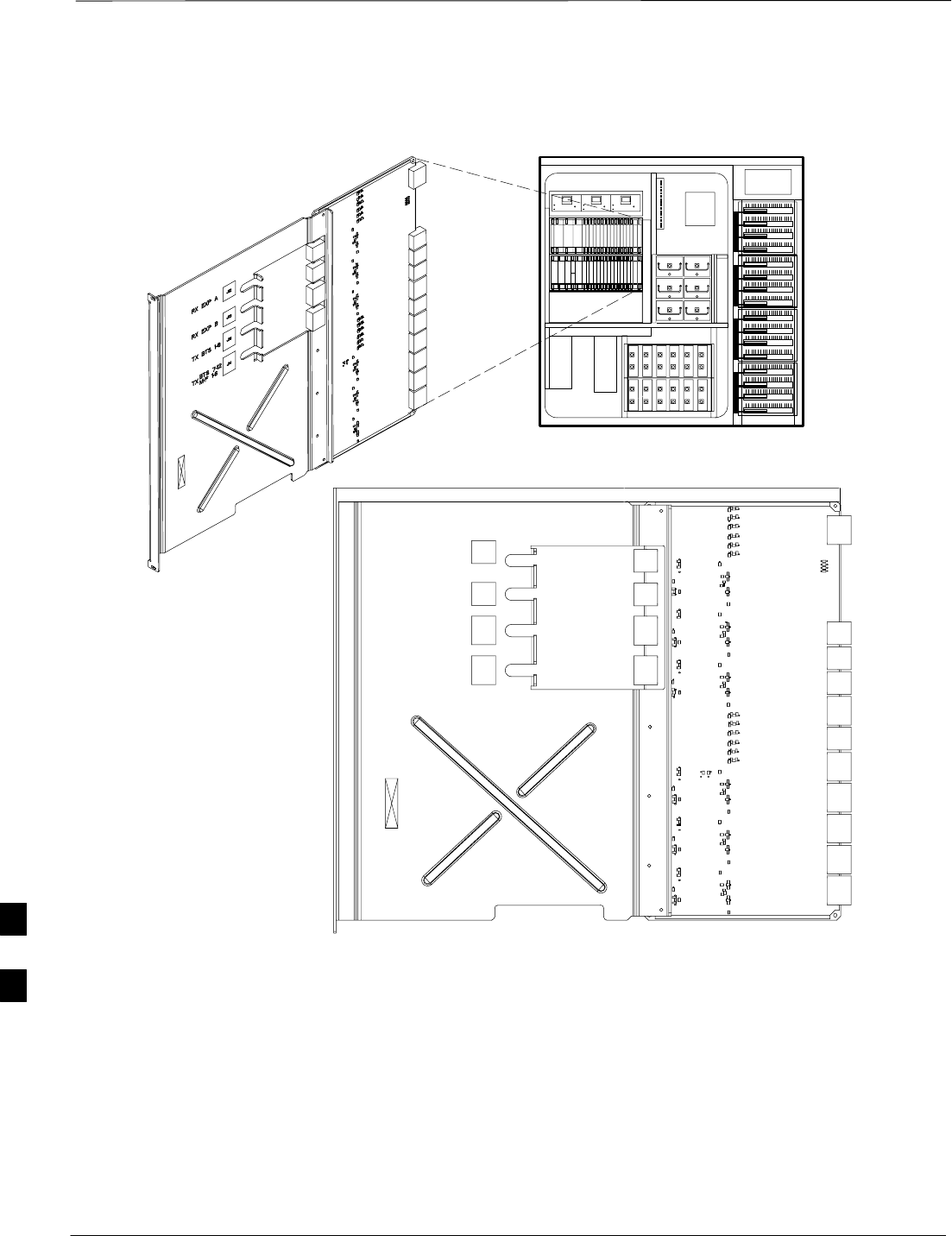
RF Cabinet LPA Cables
There can be a maximum of 16 LPAs in an RF cabinet. The connections
shown are for one LPA backplane which controls four LPAs. The
remaining LPAs are connected in the same manner. Refer to Figure H-4,
through Figure H-8 for the cables connected to the LPAs in the 4812ET
RF cabinet.
Figure H-4: LPAs for the SC 4812ET
5 RU RACK
SPACE
RFDS
EBA
ETIB
Unpopulated
LPA Shelf Cover
LPA Module
(4–Each Cage)
External Blower
Assembly (EBA)
Note:
LPA Component door
not shown for clarity
SC 4812ET BTS RF Cabinet
FW00173
H
RF Cabinet Interconnect Cables – continued
SCt4812ET BTS Optimization/ATP — CDMA LMF Jan 2002
H-8
5 RU RACK SPACE
RFDS
EBA
ETIB
SC 4812ET BTS
RF Cabinet
FW00708–REF
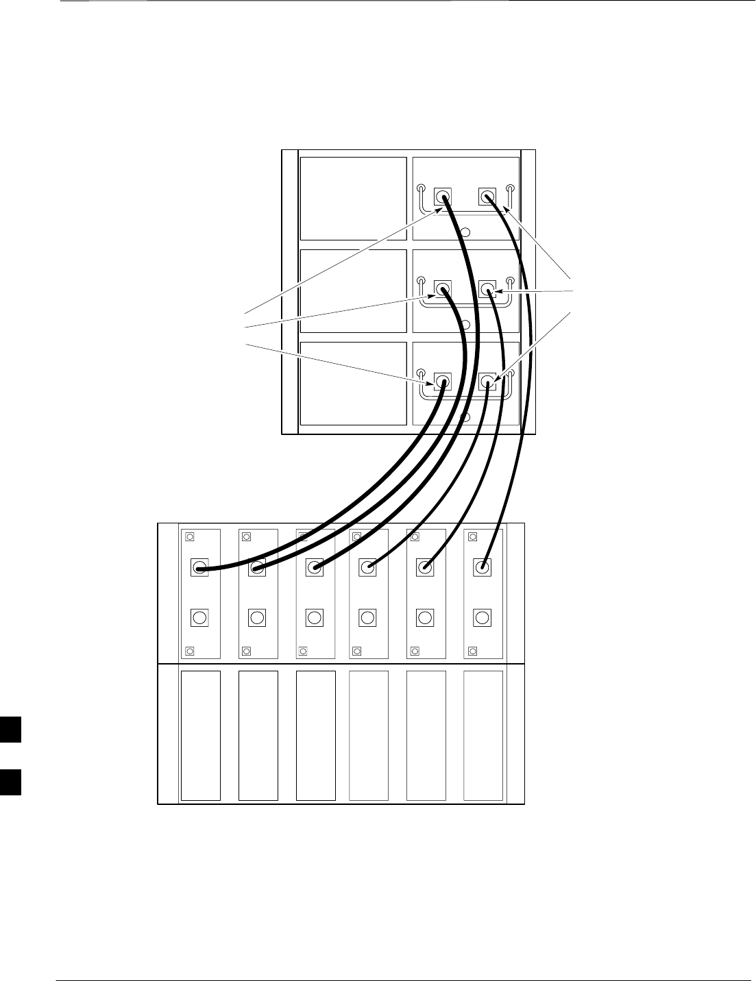
Figure H-5: BTS Combiner to LPA Backplane Cables
C1
C2
C3
C4
S1
S2
S3
LPA–1
LPA–2
LPA–3
LPA–4
TX
OUT1
TX
OUT2
TX
OUT3
TX
IN 3
TX
IN2
TX
IN 1
Cable
3064735A10
(3 each)
LPA
Backplane
4A4B
5A
5B
6A6B
1A1B
2A2B
3A3B
S1
S2
S3
S1
S2
S3
S1
S2
S3
BACK
LPA–1
LPA–2
LPA–3
LPA–4
FROM APPROPRIATE
LPA LPA 1, LPA 2,
LPA 3, LPA 4
H
RF Cabinet Interconnect Cables – continued
Jan 2002 H-9
SCt4812ET BTS Optimization/ATP — CDMA LMF
TO J15 on CIO Board
(See Figure H-7)
5 RU RACK SPACE
RFDS
EBA
ETIB
SC 4812ET BTS
RF Cabinet
FW00711
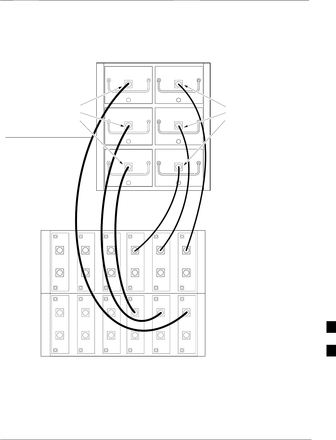
Figure H-6: Combiner to LPA Backplane/LPA Backplane To CIO Board Cables
C1
C2
C3
C4
S1
S2
S3
LPA–1
LPA–2
LPA–3
LPA–4
TX
OUT1
TX
OUT2
TX
OUT3
TX
IN 3
TX
IN2
TX
IN 1
Cable 3064735A10
(3 each)
LPA
Backplane 1
4A4B
5A
5B
6A6B
1A1B
2A2B
3A3B
S1
S2
S3
S1
S2
S3
S1
S2
S3 BLUE
GREEN
VIOLET
LPA–1
LPA–2
LPA–3
LPA–4
TX
OUT1
TX
OUT2
TX
OUT3
TX
IN 3
TX
IN2
TX
IN 1
LPA
Backplane 2
RED
YELLOW
ORANGE
Cable 3064795A05
H
RF Cabinet Interconnect Cables – continued
SCt4812ET BTS Optimization/ATP — CDMA LMF Jan 2002
H-10
Figure H-7: Components Located on CIO Card
RX EXP A
RX EXP B
TX BTS 1–6
J12
J13
J14
J15
BTS 7–12
M/F 1–6
TX
SC 4812ET RF Cabinet
FW00237
5 RU RACK
SPACE
RFDS
EBA
ETIB
H
RF Cabinet Interconnect Cables – continued
Jan 2002 H-11
SCt4812ET BTS Optimization/ATP — CDMA LMF
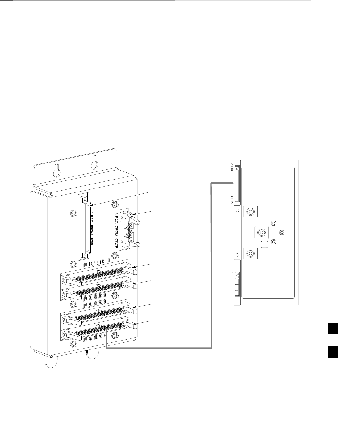
LPAC Cabling
The LPAC module provides the communication interface from the ETIB
and C–CCP to the LPA through the trunking backplane. The LPAC
interface board is contained in a protective housing which is mounted on
the RF cabinet frame behind the ETIB module. See Figure H-3,
Figure H-8 and Figure H-9 for connecting cables and connector
locations.
The LPAC is located internally to the frame as shown in Figure H-1.
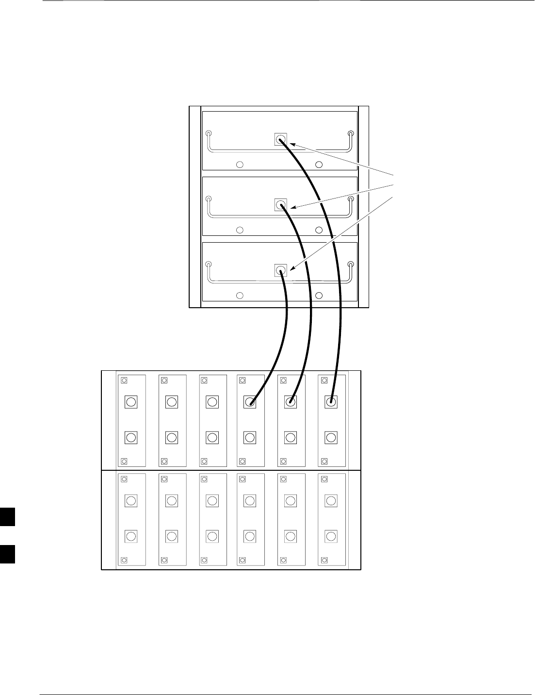
Figure H-8: LPAC Interface Board Connectors and Attaching Cable Numbers
NOTE: The LPAC is Located
Behind the ETIB Module
LPAC INTERFACE
BOARD
LPA 1A, 1B 1C, 1D
RIBBON CABLE
3086566H01
LPA 2A, 2B 2C, 2D
RIBBON CABLE
3086566H01
LPA 3A, 3B 3C, 3D
RIBBON CABLE
3086566H01
LPA 4A, 4B 4C, 4D
RIBBON CABLE
3086566H01
LPA–1
LPA–2
LPA–3
LPA–4
FRONT
TX
OUT1
TX
OUT2
TX
OUT3
TX IN 3
TX
IN2
TX IN
1
LPA BACKPLANE
1, 2, 3, & 4
Cable # 3086566H01
(4 Connections each Side)
ALARM RIBBON
CABLE TO ETIB
3086655H02
RIBBON CABLE TO
C–CCP BACKPLANE
3064794A03
FW00702
H
RF Cabinet Interconnect Cables – continued
SCt4812ET BTS Optimization/ATP — CDMA LMF Jan 2002
H-12
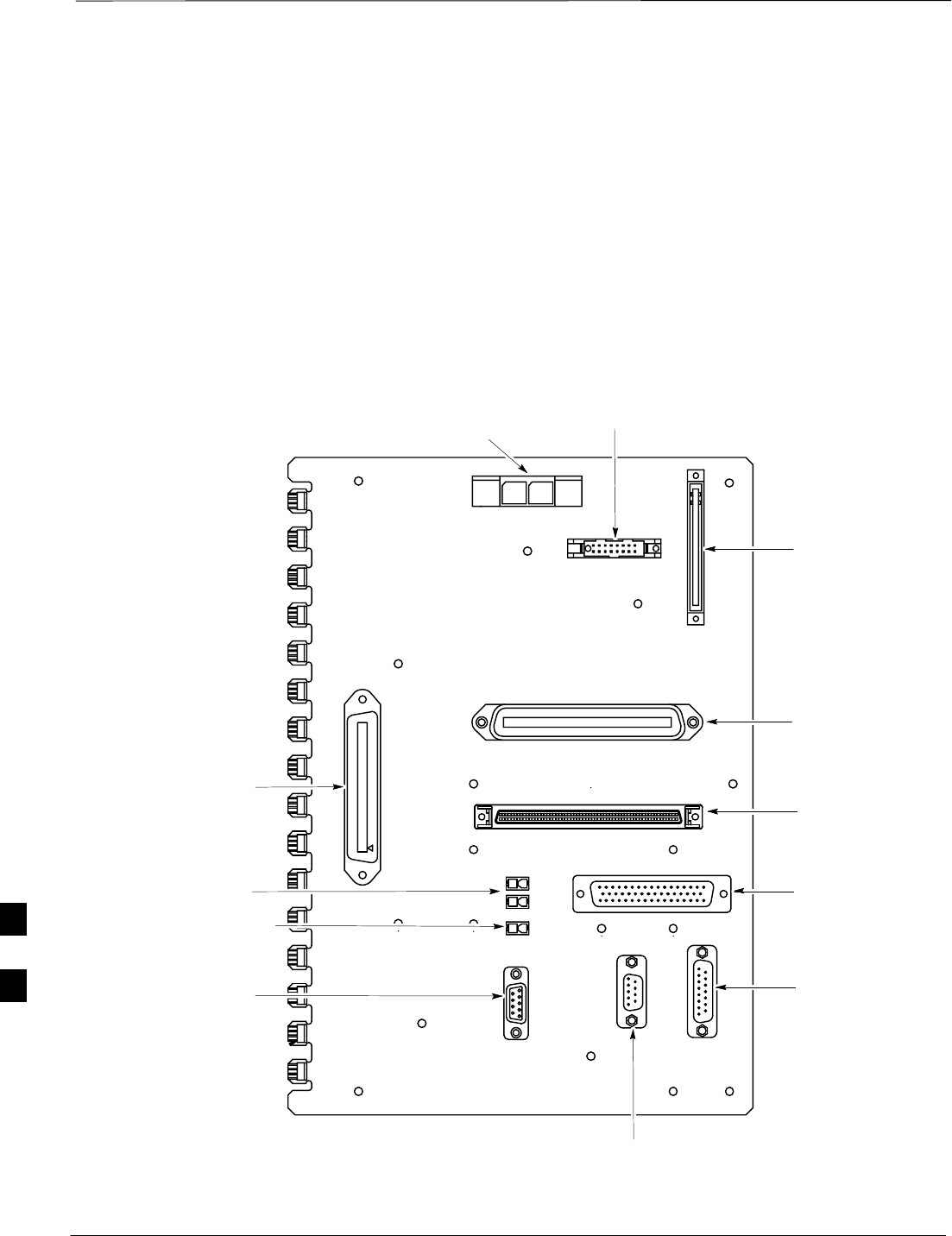
ETIB Cables and Cable
Connectors
The ETIB module (see Figure H-9) provides the interface for the LPA’s
through the LPAC, punchblock, heat exchanger and alarms to the
C–CCP backplane. The ETIB interface board is contained in a protective
housing which is mounted on the RF cabinet frame.
The ETIB is located internally to the frame as shown in Figure H-1.
SITE I/O (C–CCP Backplane)
Figure H-9: ETIB I/O Connectors and Attaching Cable Numbers
FW00701
P7
RFDS
J6
DC POWER
(Reserved) J1 To ALARMS OUT
(C–CCP Backplane)
P2
LPAC
P9 ALARMS IN
(From Bulkhead )
RGD/RGPS
P8 OPTIONS
RECEPTACLE
Cable #
3064794A05
Cable #
3086655H02
Cable #
3064534A08
Cable #
3086086H02
Cable #
3086000H02
Cable #
3086433H04
Cable #
3086366H02
J2
J5
LFR/HSO
J3
J4
HEAT EXCH
(See Figure H-16)
See Figure 2-5
and Figure H-3
See Figure 2-5
and Figure H-3
See Figure 2-5
and Figure H-3
Cable #
3086500h01
(See Figure H-8)
(See Figure H-1)
(See Figure H-1)
Cable #
3086168H01
Cable #
3086569h01
DOOR INTRUSION ALARM
H

RF Cabinet Interconnect Cables – continued
Jan 2002 H-13
SCt4812ET BTS Optimization/ATP — CDMA LMF
SPAN I/O Cable Connection
Diagram
The SPAN I/O card provides the frame interface and secondary surge
protection for the T1 lines. There are two span cards in an RF cabinet.
SPAN I/O A supports spans A, C, and E. SPAN I/O B supports span B,
D, and F. See Figure H-10 for SPAN cables and cable connections.
The SPAN I/O is located internally to the frame as shown in Figure H-1.
. . . continued on next page
H
RF Cabinet Interconnect Cables – continued
SCt4812ET BTS Optimization/ATP — CDMA LMF Jan 2002
H-14
Figure H-10: SPAN I/O Cables and Connectors
SPAN I/O (A & B)
Interface Module
RF Expansion Ports
Punch
Block Power Input
27V Ret
Antenna’s
1A 2A 3A 1B 2B 3B
4A 5A 6A 4B 5B 6B
1A 2A 3A 1B 2B 3B
4A 5A 6A 4B 5B 6B
1
2
Remote
ASU
GND
Lugs
50 Pair
(Alarms/
Punchblock
20 Pair
(RGPS)
RGD
Board
RGD/RGPS
Power Input
+27V
Micro–
wave
RF
GPS
A
B
IN OUT
LAN
19 MHz
2 Sec
Spans
Alams
Modem
Spans)
SLOT 1SLOT 2 T1 TERMINAL T1 TERMINAL
CONTROL
PORT GROUP
ADDRESS SHELF
ADDRESS
T1 DDS T1 DDS
DTE DCEDATA PORT DATA PORT
CSU Back View
NETWORK NETWORK
To/From
Network
To/From
GLI To/From
Network
To/From
GLI
Bulkhead
SPAN I/O
Connector
3086601H01 CSU 3086601H02
SPAN I/O BSPAN I/O A
3086001H02
SPAN I/O WIRING DIAGRAM
C–CCP
Backplane
4812ET Rear Connector Panel
(Located Behind
the LPAC Module,
See Figure H-1)
SPAN I/O A
3086001H02
SPAN I/O B
Bulkhead
FW00703
H

RF Cabinet Interconnect Cables – continued
Jan 2002 H-15
SCt4812ET BTS Optimization/ATP — CDMA LMF
DRDC/TRDC Cables and Cable
Connections
The DRDC is a Duplexer, RX Filter, and Directional Coupler which
provides the RF interface at the rear of the cabinet. The connections are
the antenna connection (outside rear), transmit into the DRDC TX filter.
Receive out of DRDC (RX filter), and Directional coupler.
The TRDC is a TX filter/RX filter/Directional Coupler that is the same
as the DRDC except the TRDC has two antenna outputs (TX only and
RX only) The TRDC is not available in the 1.9 GHz band.
See Figure H-11, Figure H-12, Figure H-13, and Figure H-14 for the
cable diagram that fits the configuration of your BTS site.
. . . continued on next page
H
RF Cabinet Interconnect Cables – continued
SCt4812ET BTS Optimization/ATP — CDMA LMF Jan 2002
H-16
COMBINER CAGE
FW00704
Figure H-11: 3 Sector, 2 Carrier BTS Combiner DRDC/TRDC Cable Connection
1A1B
2A2B
3A3B
1A2A3A1B2B3B
3 Sector, 2 Carrier Maximum
1–1B 3064735A11 3 SEC
2–2B 3064735A07 3 SEC
3–3B 3064735A07 3 SEC
1–1A 3064735A11 3 SEC
2–2A 3064735A07 3 SEC
3–3A 3064735A07 3 SEC
Add the following
cables for 2nd Carrier
DRDCs
Dual Bandpass Filters
H
RF Cabinet Interconnect Cables – continued
Jan 2002 H-17
SCt4812ET BTS Optimization/ATP — CDMA LMF
* FOR 3 SECTOR–4 CARRIER
Connect Combiner 4 to 1B
Combiner 5 to 2B
Combiner 6 to 3B
COMBINER CAGE
FW00705
14
25
3
6
1A2A3A1B2B3B
2 to 1 Combiners
2 Carrier – 6 Sector
4–4A 3064735A12 6 SEC
5–5A 3064735A11 6 SEC
6–6A 3064735A07 6 SEC
1–1A 3064735A11 3/6 SEC
2–2A 3064735A07 3/6 SEC
3–3A 3064735A07 3/6 SEC
DRDCs
Figure H-12: BTS 2 to 1, 3 or 6 Sector Combiner DRDC/TRDC Cable Connection
4A5A6A4B5B6B
H
RF Cabinet Interconnect Cables – continued
SCt4812ET BTS Optimization/ATP — CDMA LMF Jan 2002
H-18
FW00706
1A
2A
3A
1A2A3A1B2B3B
4 to 1 Combiners
3 Sector
1–1A 3064735A11 3 SEC
2–2A 3064735A07 3 SEC
3–3A 3064735A07 3 SEC
COMBINER CAGE
DRDCs
Figure H-13: BTS Combiner DRDC/TRDC Cable Connection
4A5A6A4B5B6B
H