Nokia Solutions and Networks T5CT1 Cellular CDMA base station User Manual IHET5CT1 GLI3 Manual 6 of 6
Nokia Solutions and Networks Cellular CDMA base station IHET5CT1 GLI3 Manual 6 of 6
Contents
- 1. IHET5CT1 GLI2 Manual 1 of 6
- 2. IHET5CT1 GLI2 Manual 2 of 6
- 3. IHET5CT1 GLI2 Manual 3 of 6
- 4. IHET5CT1 GLI2 Manual 4 of 6
- 5. IHET5CT1 GLI2 Manual 5 of 6
- 6. IHET5CT1 GLI2 Manual 6 of 6
- 7. IHET5CT1 GLI3 Manual 1 of 6
- 8. IHET5CT1 GLI3 Manual 4 of 6
- 9. IHET5CT1 GLI3 Manual 5 of 6
- 10. IHET5CT1 GLI3 Manual 6 of 6
IHET5CT1 GLI3 Manual 6 of 6
Intra-Cabinet Cabling68P09255A57-2
Aug 2002 SCt4812ET Optimization/ATP Manual Software Release R16.1.x.x
PRELIMINARY
H-17
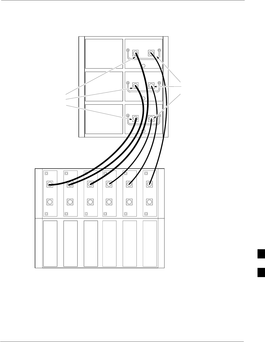
Figure H-11: 3 Sector, 2 Carrier BTS Combiner DRDC/TRDC Cable Connection
COMBINER CAGE
FW00704
1A1B
2A2B
3A3B
1A2A3A1B2B3B
3 Sector, 2 Carrier Maximum
1-1B 3064735A11 3 SEC
2-2B 3064735A07 3 SEC
3-3B 3064735A07 3 SEC
1-1A 3064735A11 3 SEC
2-2A 3064735A07 3 SEC
3-3A 3064735A07 3 SEC
Add the following
cables for 2nd Carrier
DRDCs
Dual Bandpass Filters
H
Intra-Cabinet Cabling 68P09255A57-2
Aug 2002
SCt4812ET Optimization/ATP Manual Software Release R16.1.x.x
PRELIMINARY
H-18
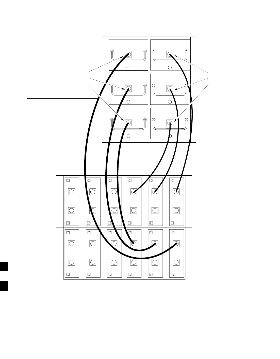
Figure H-12: BTS 2 to 1, 3 or 6 Sector Combiner DRDC/TRDC Cable Connection
* FOR 3 SECTOR-4 CARRIER
Connect Combiner 4 to 1B
Combiner 5 to 2B
Combiner 6 to 3B
COMBINER CAGE
FW00705
14
25
3
6
1A2A3A1B2B3B
2 to 1 Combiners
2 Carrier - 6 Sector
4-4A 3064735A12 6 SEC
5-5A 3064735A11 6 SEC
6-6A 3064735A07 6 SEC
1-1A 3064735A11 3/6 SEC
2-2A 3064735A07 3/6 SEC
3-3A 3064735A07 3/6 SEC
DRDCs
4A5A6A4B5B6B
H
Intra-Cabinet Cabling68P09255A57-2
Aug 2002 SCt4812ET Optimization/ATP Manual Software Release R16.1.x.x
PRELIMINARY
H-19
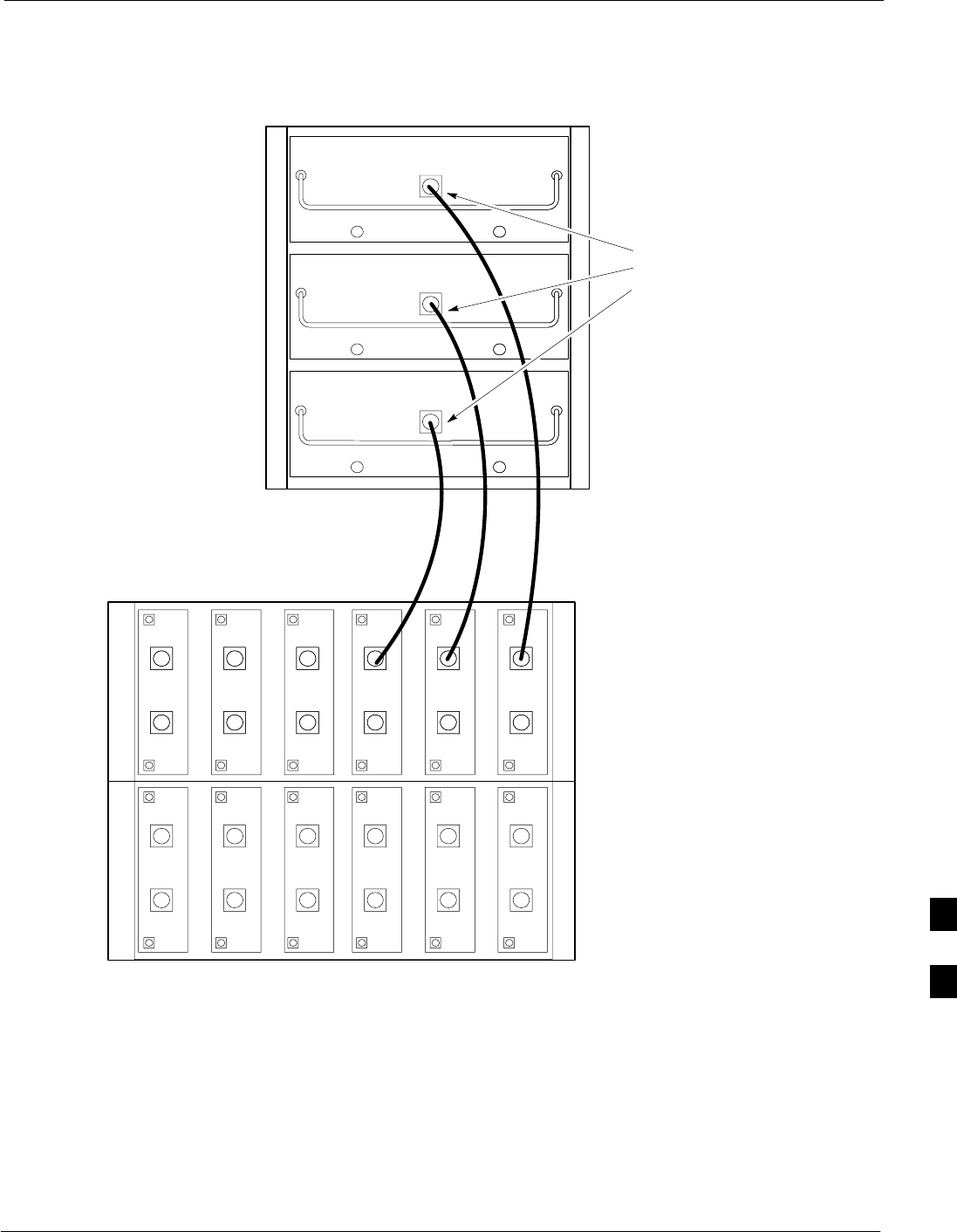
Figure H-13: BTS Combiner DRDC/TRDC Cable Connection
FW00706
1A
2A
3A
1A2A3A1B2B3B
4 to 1 Combiners
3 Sector
1-1A 3064735A11 3 SEC
2-2A 3064735A07 3 SEC
3-3A 3064735A07 3 SEC
COMBINER CAGE
DRDCs
4A5A6A4B5B6B
H
Intra-Cabinet Cabling 68P09255A57-2
Aug 2002
SCt4812ET Optimization/ATP Manual Software Release R16.1.x.x
PRELIMINARY
H-20
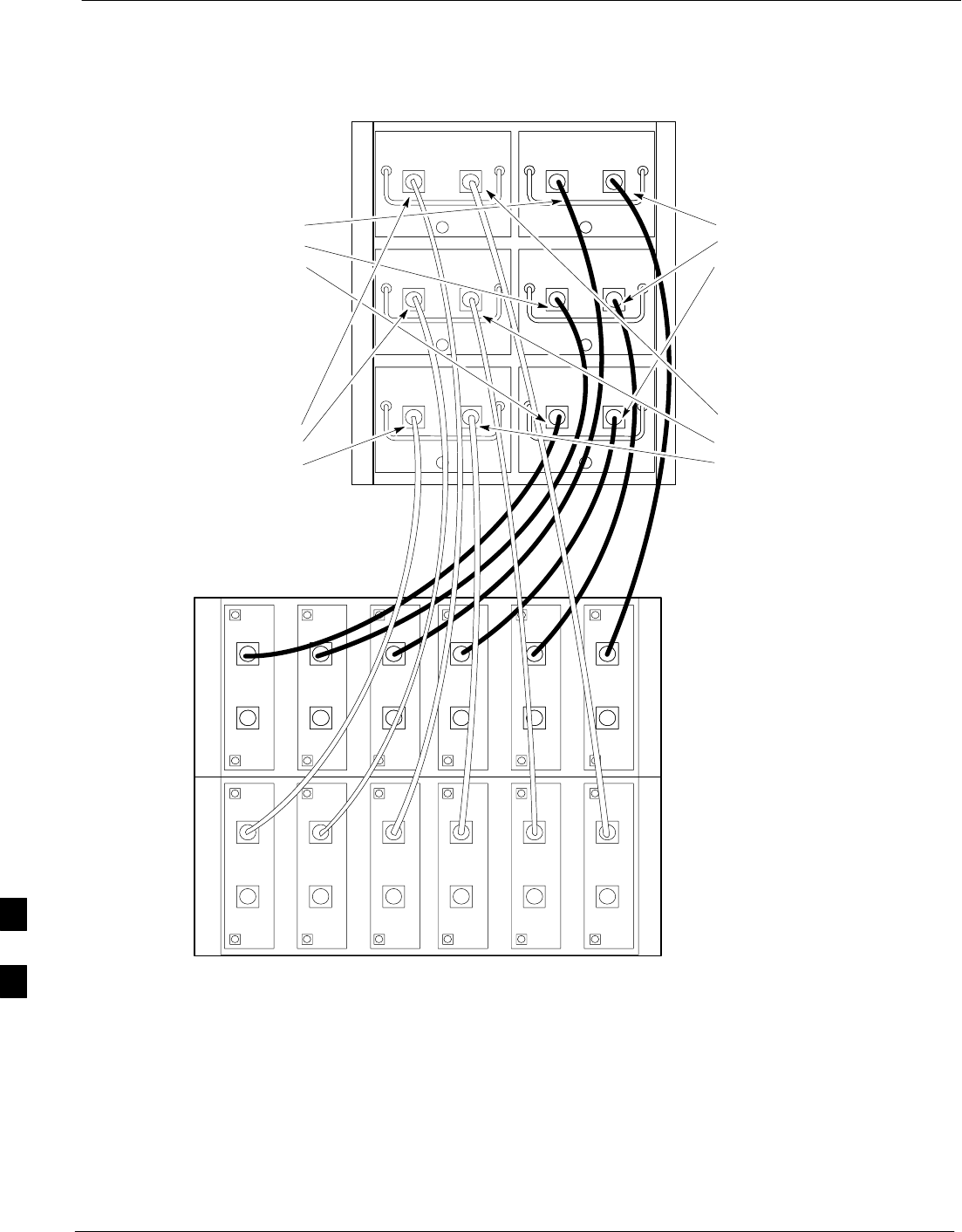
Figure H-14: SC 4812ET BTS Combiner DRDC/TRDC Cable Connection
4A4B
5A
5B
6A6B
FW00707
1A1B
2A2B
3A3B
1A2A3A1B2B3B
Dual Bandpass Filter
6 Sector - 1 or 2 Carrier
1-1B 3064735A11 6 Sec
2-2B 3064735A07 6 Sec
3-3B 3064735A07 6 Sec
1-1A 3064735A11 6 Sec
2-2A 3064735A07 6 Sec
3-3A 3064735A07 6 Sec
COMBINER CAGE
DRDCs
4A5A6A4B5B6B
4-4A 3064735A12 6 Sec
5-5A 3064735A11 6 Sec
6-6A 3064735A07 6 Sec
4-4B 3064735A12 6 Sec
5-5B 3064735A11 6 Sec
6-6B 3064735A07 6 Sec
H

Intra-Cabinet Cabling68P09255A57-2
Aug 2002 SCt4812ET Optimization/ATP Manual Software Release R16.1.x.x
PRELIMINARY
H-21
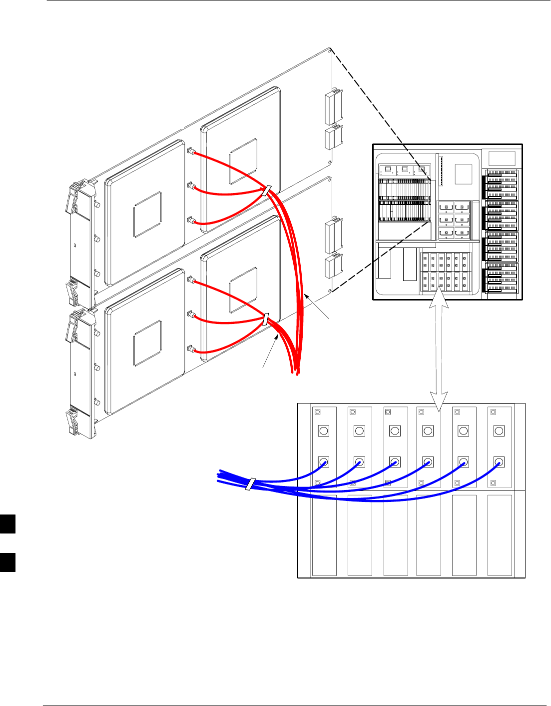
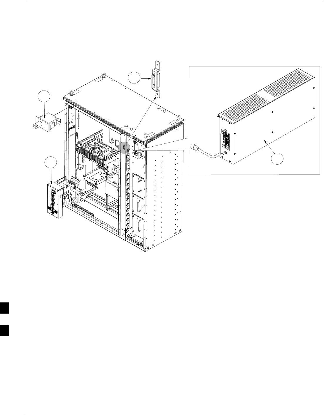
MPC Functional Description
The MPC card provides (see Figure H-15) low-noise amplification for
all RX path signals. The low noise, high gain design improves frame RX
sensitivity and overcomes the splitting loss in the receive path. DC
voltages are monitored on the RF devices and regulators and are used to
generate hard and soft alarms. The MPC is not redundant at the
card-level, but includes dual-path amplifiers which provide soft-fail
redundancy for all sectors.
MPC to DRDC Cabling
The cables connecting the MPC cards to the DRDCs for a three sector
RF cabinet are shown in Figure H-15. A six sector RF cabinet would
have six more DRDC’s and they would be connected to the front of the
MPC cards.
H
Intra-Cabinet Cabling 68P09255A57-2
Aug 2002
SCt4812ET Optimization/ATP Manual Software Release R16.1.x.x
PRELIMINARY
H-22
Figure H-15: DRDC To C-CCP Cage MPC Boards Cable Connections
5 RU RACK
SPACE
RFDS
EBA
ETIB
SC 4812ET
RF Cabinet
FW00710
1A2A3A1B2B3B
1A - 3A: CABLE # 3086659H01
1B - 3B: CABLE # 3086659H01
DRDC CAGE
CABLES CONNECT
1A, 2A, 3A TO TOP
MPC BOARD
# 3086659H01
MPC BOARDS
CABLES CONNECT
1B, 2B, 3B TO
BOTTOM MPC BOARD
# 3086659H01
* Use Cable 3086659H02
For Sectors 4 - 6
H
Intra-Cabinet Cabling68P09255A57-2
Aug 2002 SCt4812ET Optimization/ATP Manual Software Release R16.1.x.x
PRELIMINARY
H-23
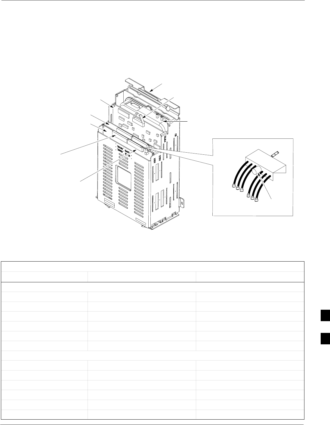
RFDS Cabling Details
Figure H-16 shows the components of the RFDS. Table H-2 depicts the
cabling for a 3-Sector Duplexed configuration and Table H-3 depicts the
cabling for a 6-Sector Duplexed configuration. Figure H-17 shows the
connection of the RFDS to the BTS combiners.
Figure H-16: RFDS Component Identification
ASU1
REFL/ANT PORTS 1
THROUGH 6
SUBSCRIBER
UNIT ASSEMBLY
AMR BUS/POWER
CONNECTOR (LR485)
FWTIC
FWD/BTS PORTS
1 THROUGH 6
HANDLE
ASU2
P2
P3
MCX
CONNECTOR
TO ASU
SMA CONNECTORS
TO DRDC BTS OR
ANT PORTS
MCX CABLE DETAIL
KNURLED
LOCK
SCREWS
CONNECTS to P2 AND
P3 OF ASU1 AND ASU2
FW00217-REF
Cable #
3064794A05
(See Figure H-9)
(See Figure H-17)
(See Figure H-17)
(See Figure H-17)
Table H-2: SC 4812ET Series 3-Sector Duplexed Directional Coupler to RFDS Cabling Table
DRDC Label Directional Coupler Port Cobra RFDS Port
ASU 1 - FWD (six pack MCX)
1A BTS Sector 1 Main BTS ASU1-FWD BTS-1
1B BTS Sector 1 Diversity BTS ASU1-FWD BTS-2
2A BTS Sector 2 Main BTS ASU1-FWD BTS-3
2B BTS Sector 2 Diversity BTS ASU1-FWD BTS-4
3A BTS Sector 3 Main BTS ASU1-FWD BTS-5
3B BTS Sector 3 Diversity BTS ASU1-FWD BTS-6
ASU 1 - REF (six pack MCX)
1A ANT Sector 1 Main ANT ASU1-REF ANT-1
1B ANT Sector 1 Diversity ANT ASU1-REF ANT-2
2A ANT Sector 2 Main ANT ASU1-REF ANT-3
2B ANT Sector 2 Diversity ANT ASU1-REF ANT-4
3A ANT Sector 3 Main ANT ASU1-REF ANT-5
3B ANT Sector 3 Diversity ANT ASU1-REF ANT-6
H

Intra-Cabinet Cabling 68P09255A57-2
Aug 2002
SCt4812ET Optimization/ATP Manual Software Release R16.1.x.x
PRELIMINARY
H-24
Table H-3: SC 4812ET Series 6-Sector Duplexed Directional Coupler to RFDS Cabling Table
DRDC Label Directional Coupler Port Cobra RFDS Port
ASU 1 - FWD (six pack MCX)
1A BTS Sector 1 Main BTS ASU1-FWD BTS-1
1B BTS Sector 1 Diversity BTS ASU1-FWD BTS-2
2A BTS Sector 2 Main BTS ASU1-FWD BTS-3
2B BTS Sector 2 Diversity BTS ASU1-FWD BTS-4
3A BTS Sector 3 Main BTS ASU1-FWD BTS-5
3B BTS Sector 3 Diversity BTS ASU1-FWD BTS-6
ASU 2 - FWD (six pack MCX)
4A BTS Sector 4 Main BTS ASU2-FWD BTS-1
4B BTS Sector 4 Diversity BTS ASU2-FWD BTS-2
5A BTS Sector 5 Main BTS ASU2-FWD BTS-3
5B BTS Sector 5 Diversity BTS ASU2-FWD BTS-4
6A BTS Sector 6 Main BTS ASU2-FWD BTS-5
6B BTS Sector 6 Diversity BTS ASU2-FWD BTS-6
ASU 1 - REF (six pack MCX)
1A ANT Sector 1 Main ANT ASU1-REF ANT-1
1B ANT Sector 1 Diversity ANT ASU1-REF ANT-2
2A ANT Sector 2 Main ANT ASU1-REF ANT-3
2B ANT Sector 2 Diversity ANT ASU1-REF ANT-4
3A ANT Sector 3 Main ANT ASU1-REF ANT-5
3B ANT Sector 3 Diversity ANT ASU1-REF ANT-6
ASU 2 - REF (six pack MCX)
4A ANT Sector 4 Main ANT ASU2-REF ANT-1
4B ANT Sector 4 Diversity ANT ASU2-REF ANT-2
5A ANT Sector 5 Main ANT ASU2-REF ANT-3
5B ANT Sector 5 Diversity ANT ASU2-REF ANT-4
6A ANT Sector 6 Main ANT ASU2-REF ANT-5
6B ANT Sector 6 Diversity ANT ASU2-REF ANT-6
H
Intra-Cabinet Cabling68P09255A57-2
Aug 2002 SCt4812ET Optimization/ATP Manual Software Release R16.1.x.x
PRELIMINARY
H-25
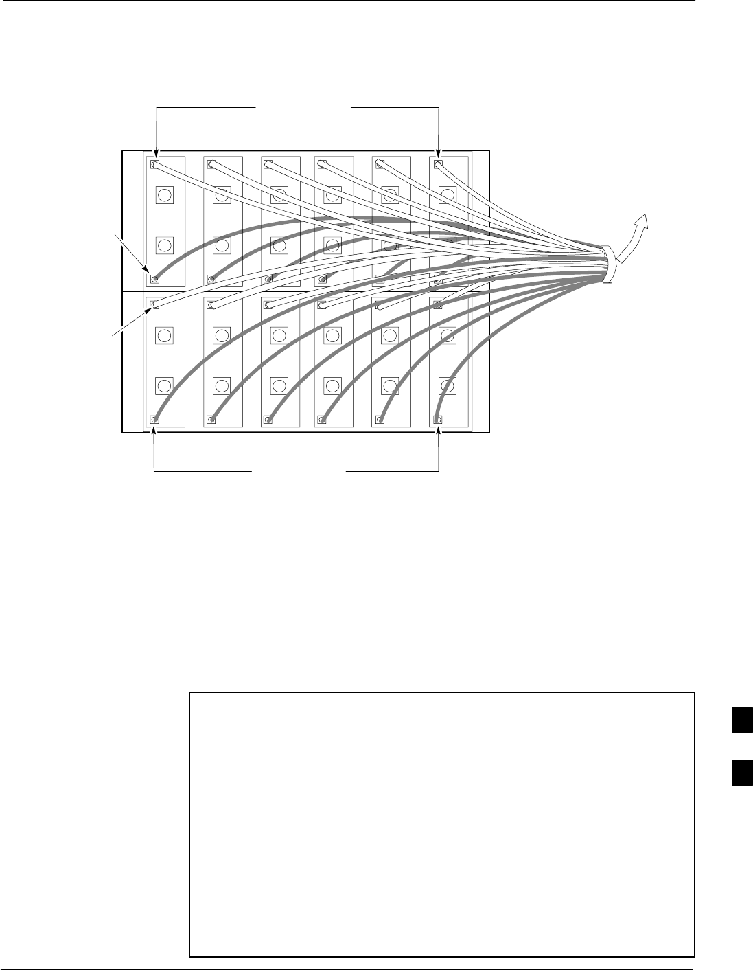
Figure H-17: SC 4812ET BTS Combiner DRDC/TRDC RFDS Cable Connection
1A2A3A1B2B3B
4A5A6A4B5B6B
FW00709
ANT COUPLED
TO RFDS ASU 1
ANT COUPLED
TO RFDS ASU 2
(See Figure H-16)
(See Figure H-16)
DRDC CAGE
BTS COUPLED
TO RFDS ASU 2
(See Figure H-16)
BTS COUPLED
TO RFDS ASU 1
(See Figure H-16)
TO RFDS
ASU1 & ASU2
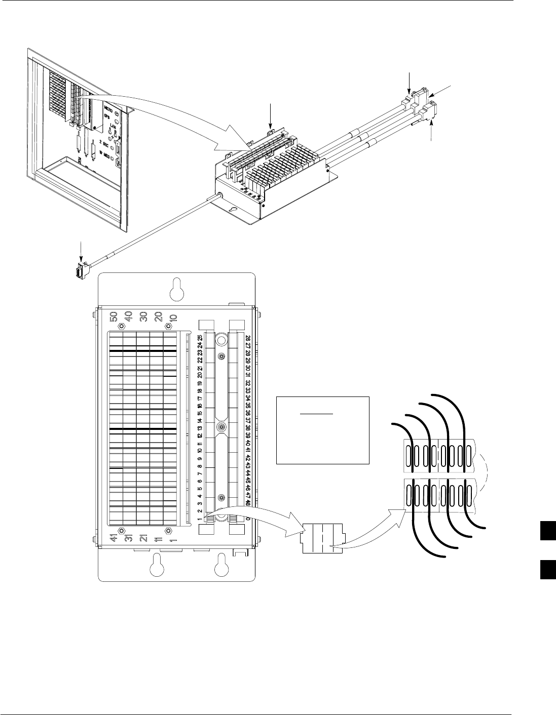
50 Pair Punchblock
The 50 pair punchblock is the main interface point for RGPS, span lines,
customer I/O, Power Cabinet alarm lines, and the modem. The
punchblock provides primary protection for all lines. Refer to
Figure H-18 and Table H-4 for punchblock pin-out.
CAUTION SC4812ET Span Line Labeling for Span B and Span C is
swapped
- On the SC4812ET’s, the span cabel internal to the base station
that connects the 50 pin header on the I/O plate to the CSU has
Span B and Span C (RJ-45) connectors mis-labeled.
- CFE will punch down the span on the 50 pair bunchblock as
per Motorola documentation and punchdown chart. When con-
ecting the span input to the CSU re-label “Span B” cable
to”Span C” cable to “Span B”. Connect to CSU as per docu-
mentation
- Note: The labeling issue on the cable from the I/O plate to the
CSU Part Number 3086601H01 Rev C shall be corrected on
revision “D” to address this issue. The cut over date to Rev. D
will be approximately January 30, 2001.
H

Intra-Cabinet Cabling 68P09255A57-2
Aug 2002
SCt4812ET Optimization/ATP Manual Software Release R16.1.x.x
PRELIMINARY
H-26
CAUTION A wiring discrepancy exists between the manuals and the frame
for remote GPS.
- The TX and RX are reversed in the ETIB, leading to inoper-
ability of the RGPS. The RGPS will not work in either a single
standalone or multiple frame configuration.
- Swap the White and White/Bk wires to punch pins 44T and
44R. The Green and Green/Bk go to 45T and 45R. This will
correct non-expansion configurations.
- Single frame and expansion BTSs without RGPS can use this
workaround as a permanent solution.
- For expansion with RGPS required a new cable (P/N
3086433H10 ) will correct the problem.
H
Intra-Cabinet Cabling68P09255A57-2
Aug 2002 SCt4812ET Optimization/ATP Manual Software Release R16.1.x.x
PRELIMINARY
H-27
Figure H-18: 50 Pair Punchblock
TOP VIEW OF
PUNCH BLOCK
STRAIN RELIEVE
INCOMING CABLE TO
BRACKET WITH TIE WRAPS
2T
1T 1R 2T 2R
12
1R
2R
LEGEND
1T = PAIR 1 - TIP
1R = PAIR 1 -RING
” ”
” ”
” ”
RF Cabinet I/O Area
50R
50T
49R
49T
1T
FW00162-REF
TO SPAN
CONNECTOR
TO ALARMS
CONNECTOR
TO MODEM
CONNECTOR
TO RGD/RGPS
CONNECTOR
SeeTable H-4
for Pin-Out.
H

Intra-Cabinet Cabling 68P09255A57-2
Aug 2002
SCt4812ET Optimization/ATP Manual Software Release R16.1.x.x
PRELIMINARY
H-28
Alarm and Span Line Cable Pin/Signal Information
Table H-4 lists the complete pin/signal identification for the 50-pin
punch block.
Table H-4: Pin-Out for 50-Pair Punchblock
Punchblock
Cable
Connector Function Signal Name Punch Pin Ext. Cable Wire
Color
Power Cab Control - NC 1T Blue
Power Cab Control - NO 1R Blk/Blue
Power Cab Control-Com 2T Yellow
Reserved 2R N/C
Rectifier Fail 3T Blk/Yellow
AC Fail 3R Green
Power Cabinet Power Cab Exchanger Fail 4T Blk/Grn
Power Cab Door Alarm 4R White
Power Cab Major Alarm 5T Blk/White
Battery Over Temp 5R Red
Power Cab Minor Alarm 6T Blk/Red
Reticifier Over Temp 6R Brown
Power Cab Alarm Rtn 7T Blk/Brn
ALARM LFR_HSO_GND 7R
HSO/LFR EXT_1PPS_POS 8T
Extension EXT_1PPS_NEG 8R
CAL_+ 9T
CAB_- 9R
LFR Antenna LORAN_+ 10T
LORAN_- 10R
Pilot Beacon Alarm - Minor 11T
Pilot Beacon Alarm - Rtn 11R
Pilot Beacon Alarm - Major 12T
Pilot Beacon Pilot Beacon Control-NO 12R
Pilot Beacon Control - COM 13T
Pilot Beacon Control - NC 13R
. . . continued on next page
H

Intra-Cabinet Cabling68P09255A57-2
Aug 2002 SCt4812ET Optimization/ATP Manual Software Release R16.1.x.x
PRELIMINARY
H-29
Table H-4: Pin-Out for 50-Pair Punchblock
Punchblock
Cable
Connector
Ext. Cable Wire
Color
Punch PinSignal Name
Function
Customer Outputs 1 - NO 14T
Customer Outputs 1 - COM 14R
Customer Outputs 1 - NO 14T
Customer Outputs 1 - COM 14R
Customer Outputs 1 - NC 15T
Customer Outputs 2 - NO 15R
Customer Outputs 2 - COM 16T
ALARM Customer Outputs Customer Outputs 2 - NC 16R
Customer Outputs 3 - NO 17T
Customer Outputs 3 - COM 17R
Customer Outputs 3 - NC 18T
Customer Outputs 4 - NO 18R
Customer Outputs 4-COM 19T
Customer Outputs 4 - NC 19R
Customer Inputs 1 20T
Cust_Rtn_A_1 20R
Customer Inputs 2 21T
Cust_Rtn_A_2 21R
Customer Inputs 3 22T
Cust_Rtn_A_3 22R
Customer Inputs 4 23T
Cust_Rtn_A_4 23R
Customer Inputs 5 24T
Cust_Rtn_A_5 24R
ALARM Customer Inputs Customer Inputs 6 25T
Cust_Rtn_A_6 25R
Customer Inputs 7 26T
Cust_Rtn_A_7 26R
Customer Inputs 8 27T
Cust_Rtn_A_8 27R
Customer Inputs 9 28T
Cust_Rtn_A_9 28R
Customer Inputs 10 29T
Cust_Rtn_A_10 29R
. . . continued on next page
H

Intra-Cabinet Cabling 68P09255A57-2
Aug 2002
SCt4812ET Optimization/ATP Manual Software Release R16.1.x.x
PRELIMINARY
H-30
Table H-4: Pin-Out for 50-Pair Punchblock
Punchblock
Cable
Connector
Ext. Cable Wire
Color
Punch PinSignal Name
Function
RCV_TIP_A 30T
RCV_RING_A 30R
Span 1 XMIT_TIP_A 31T
XMIT_RING_A 31R
RCV_TIP_B 32T
RCV_RING_B 32R
Span 2 XMIT_TIP_B 33T
XMIT_RING_B 33R
RCV_TIP_C (Note) 34T
RCV_RING_C (Note) 34R
Span 3 XMIT_TIP_C (Note) 35T
XMIT_RING_C(Note) 35R
RCV_TIP_D (Note) 36T
SPAN I/O RCV_RING_D (Note) 36R
Span 4 XMIT_TIP_D (Note) 37T
XMIT_RING_D(Note) 37R
RCV_TIP_E (Note) 38T
RCV_RING_E (Note) 38R
Span 5 XMIT_TIP_E (Note) 39T
XMIT_RING_E(Note) 39R
RCV_TIP_F (Note) 40T
RCV_RING_F (Note) 40R
Span 6 XMIT_TIP_F (Note) 41T
XMIT_RING_F(Note) 41R
NOTE
Span 3 through 6 are spares for expansion purposes
. . . continued on next page
H

Intra-Cabinet Cabling68P09255A57-2
Aug 2002 SCt4812ET Optimization/ATP Manual Software Release R16.1.x.x
PRELIMINARY
H-31
Table H-4: Pin-Out for 50-Pair Punchblock
Punchblock
Cable
Connector
Ext. Cable Wire
Color
Punch PinSignal Name
Function
GPS_Power_A 42T Yellow
For frame GPS_Power_A_Return 42R Yellow/Black
without RGD GPS_Power_B 43T Blue
Expansion
Punchblock GPS_Power_B_Return 43R Blue/Black
Single Frame GPS_TXD+ 44T White
RGD/RGPS BTS;RGPS Head GPS_TXD- 44R White/Black
Connection GPS_RXD+ 45T Green
OR
Multiple Frame GPS_RXD- 45R Green/Black
Multiple Frame
BTS; RGD Signal Ground (TDR+) 46T Red
Connection at Signal Ground (TDR-) 46R Red/Black
RGPS Secondary
Frame GPS_1PPS+ 47T Brown
GPS_1PPS- 47R Brown/Black
GPS_Power_A 42T Yellow
GPS_Power_A_Return 42R Yellow/Black
GPS_Power_B 43T Blue
For frame with GPS_Power_B_Return 43R Blue/Black
RGD Expansion
Punchblock GPS_TXD+ 44T White
OR GPS_TXD- 44R White/Black
RGD/RGPS Multiple Frame
BTS; RGPS Head GPS_RXD+ 45T Green
BTS; RGPS Head
Connection at GPS_RXD- 45R Green/Black
RGPS Primary
Frame Signal Ground (TDR+) 46T Red
Master Frame (TDR-) 46R Red/Black
GPS_1PPS+ 47T Brown
GPS_1PPS- 47R Brown/Black
Reserved 48T
MODEM Reserved 48R
RGD/RGPS Chassis Ground 49T N/A
None No Connection 49R None
Reserved 50T None
ALARM Reserved 50R None
H
Intra-Cabinet Cabling 68P09255A57-2
Aug 2002
SCt4812ET Optimization/ATP Manual Software Release R16.1.x.x
PRELIMINARY
H-32
RF Cabinet Parts Locator
Figure H-19 illustrates the location of door switch interlocks, DC Power
distribution and the EBA blower assembly.
Figure H-19: SC 4812ET RF Cabinet Parts Locator
FW00440-REF
2
34
1
INDEX:
1. Door Switch
2. Door Switch (Main)
3. DC Power Distribution
4. EBA Blower Assembly
H

Aug 2002 SCt4812ET Optimization/ATP Manual Software Release R16.1.x.x
PRELIMINARY
I-1
Appendix I
GPIB Addressing
I
GPIB 68P09255A57-2
Aug 2002
SCt4812ET Optimization/ATP Manual Software Release R16.1.x.x
PRELIMINARY
I-2
GPIB
GPIB Introduction
Use the procedures in this appendix to verify and/or change the GPIB
addresses of the applicable test equipment.
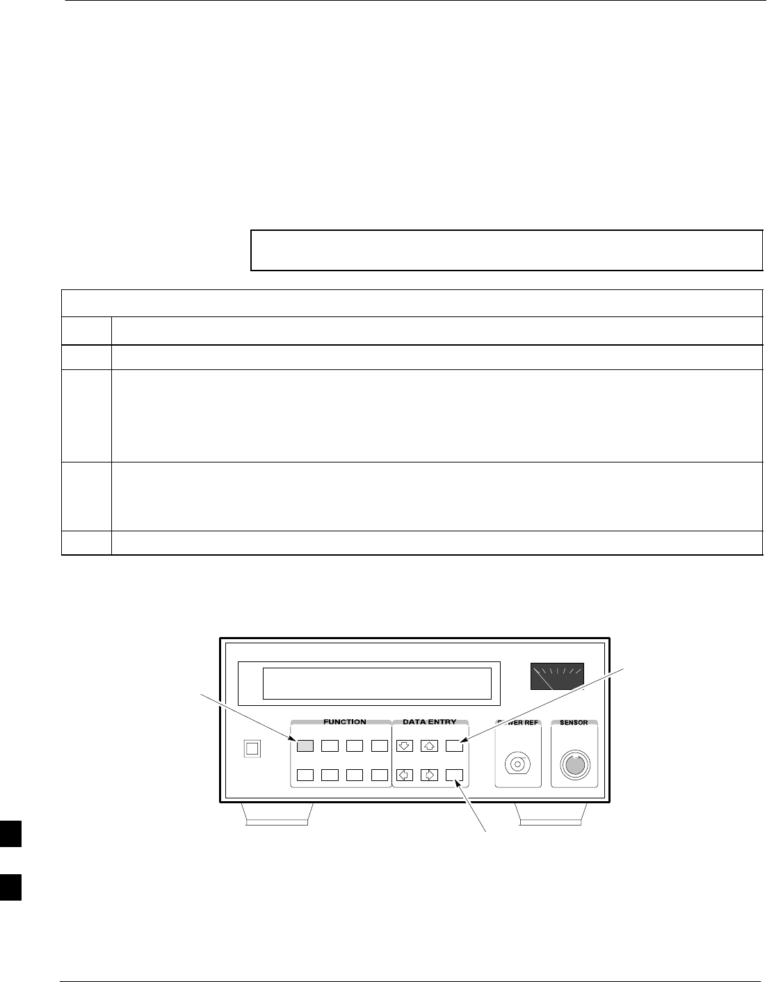
HP437 Power Meter GPIB Address
Follow the steps in Table I-1 to verify and, if necessary, change the
HP437 GPIB address.
NOTE This procedure assumes that the test equipment is set up and
ready for testing.
Table I-1: Verify and/or Change HP437 Power Meter GPIB Address
Step Action
1 Press Shift and PRESET (see Figure I-1).
2Use the y arrow key to navigate to HP-IB ADRS and press ENTER.
The HP-IB address is displayed.
NOTE
HP-IB is the same as GPIB.
3If the current GPIB address is not set to 13, perform the following to change it:
- Use the y b arrow keys to change the HP-IB ADRS to 13.
- Press ENTER to set the address.
4 Press Shift and ENTER to return to a standard configuration.
Figure I-1: HP437 Power Meter
ENTER
PRESET
SHIFT (BLUE) PUSHBUTTON -
ACCESSES FUNCTION AND
DATA ENTRY KEYS IDENTIFIED
WITH LIGHT BLUE TEXT ON
THE FRONT PANEL ABOVE
THE BUTTONS
FW00308REF
I
GPIB68P09255A57-2
Aug 2002 SCt4812ET Optimization/ATP Manual Software Release R16.1.x.x
PRELIMINARY
I-3
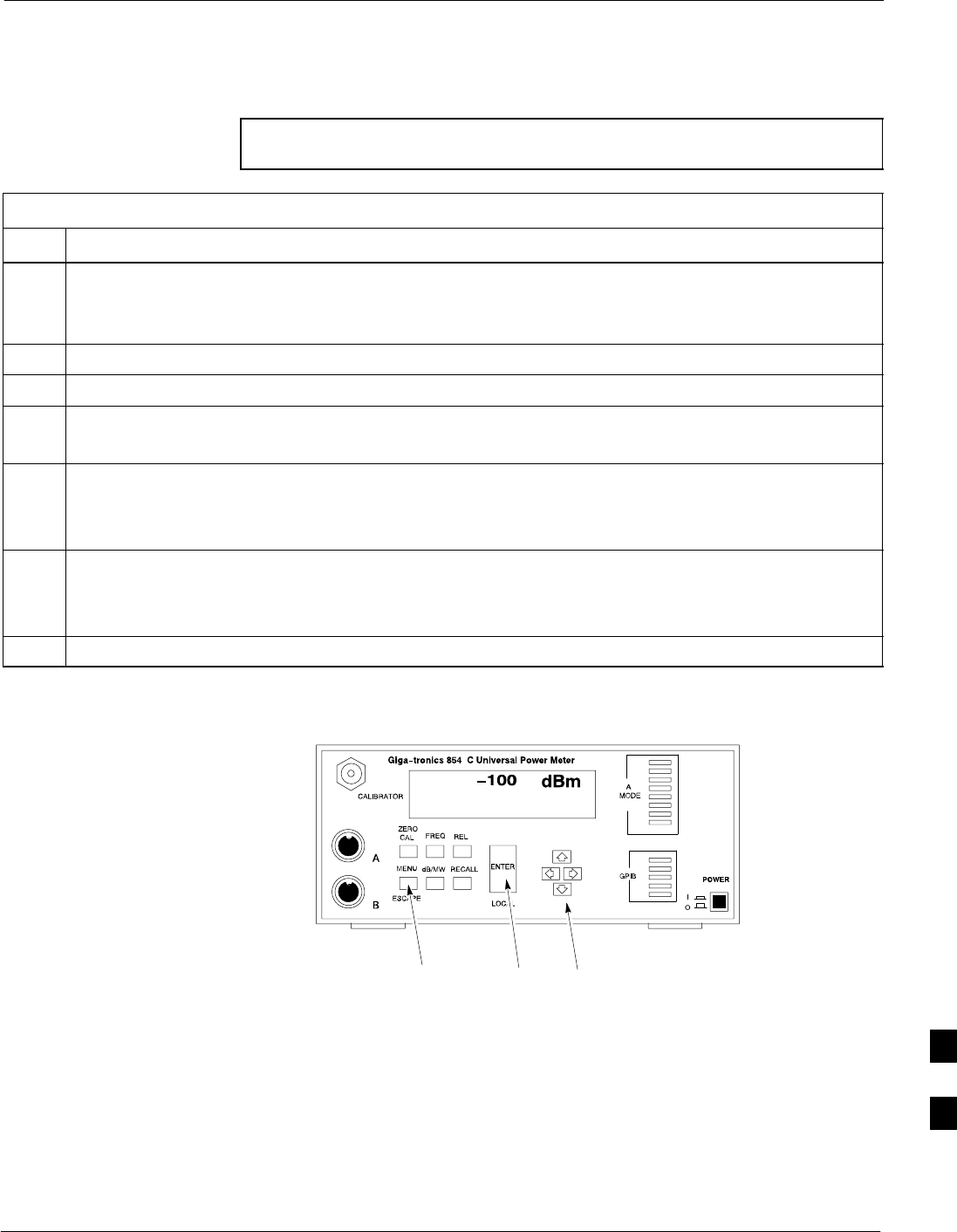
Gigatronics 8541C Power Meter GPIB Address
Follow the steps in Table I-2 to verify and, if necessary, change the
Gigatronics 8541C power meter GPIB address.
NOTE This procedure assumes that the test equipment is set up and
ready for testing.
Table I-2: Verify and/or Change Gigatronics 8541C Power Meter GPIB Address
Step Action
! CAUTION
Do not connect/disconnect the power meter sensor cable with AC power applied to the meter.
Disconnection could result in destruction of the sensing element or miscalibration.
1 Press MENU (see Figure I-2).
2Use the b arrow key to select CONFIG MENU and press ENTER.
3Use the b arrow key to select GPIB and press ENTER.
The current Mode and GPIB Address are displayed.
4If the Mode is not set to 8541C, perform the following to change it:
Use the a ' arrow keys as required to select MODE.
Use the by arrow keys as required to set MODE to 8541C.
5If the GPIB address is not set to 13, perform the following to change it:
Use the ' arrow key to select ADDRESS.
Use the by arrow keys as required to set the GPIB address to 13.
6 Press ENTER to return to normal operation.
Figure I-2: Gigatronics 8541C Power Meter Detail
MENU ENTER ARROW
KEYS REF FW00564
1
I

GPIB 68P09255A57-2
Aug 2002
SCt4812ET Optimization/ATP Manual Software Release R16.1.x.x
PRELIMINARY
I-4
Motorola CyberTest GPIB Address
Follow the steps in Table I-3 to verify and, if necessary, change the
GPIB address on the Motorola CyberTest. Changing the GPIB address
requires the following items:
SMotorola CyberTest communications analyzer
SComputer running Windows 3.1/Windows 95
SMotorola CyberTAME software program “TAME”
SParallel printer port cable (shipped with CyberTest)
NOTE This procedure assumes that the test equipment is set up and
ready for testing.
Table I-3: Verify and/or Change Motorola CyberTest GPIB Address
Step Action
1On the LMF desktop, locate the CyberTAME icon. Double click on the icon to run the CyberTAME
application.
2In the CyberTAME window taskbar, under Special, select IEEE.488.2.
3CyberTAME software will query the CyberTest Analyzer for its current GPIB address. It then will
open the IEEE 488.2 dialog box. If the current GPIB address is not 18, perform the following
procedure to change it:
- Use the up or down increment arrows, or double-click in the field and type the number.
- Click on the OK button.
The new address will be written to the CyberTest via the parallel port and saved.
NOTE
Verify that the address has been set by repeating steps 2 and 3. The new address should now appear in
the IEEE 488.2 dialog box Address field.
HP8935 Test Set GPIB Address
Follow the procedure in Table I-4 to verify and, if necessary, change the
HP8935 GPIB address.
NOTE This procedure assumes that the test equipment is set up and
ready for testing.
Table I-4: Verify and/or Change HP8935 GPIB Address
Step Action
* IMPORTANT
The HP I/O configuration MUST be set to Talk & Listen, or NO device on the GPIB bus will be
accessible. (Consult test equipment OEM documentation for additional information as required.)
1To verify that the GPIB addresses are set correctly, press Shift and LOCAL on the HP8935 (see
Figure I-3). The current HP-IB address is displayed at the top of the screen.
NOTE
HP-IB is the same as GPIB.
I
GPIB68P09255A57-2
Aug 2002 SCt4812ET Optimization/ATP Manual Software Release R16.1.x.x
PRELIMINARY
I-5
Table I-4: Verify and/or Change HP8935 GPIB Address
Step Action
2If the current GPIB address is not set to 18, perform the following to change it:
- Press Shift and Inst Config.
- Turn the Cursor Control knob to move the cursor to the HP-IB Adrs field.
- Press the Cursor Control knob to select the field.
- Turn the Cursor Control knob as required to change the address to 18.
- Press the Cursor Control knob to set the address.
3SPress Preset to return to normal operation.
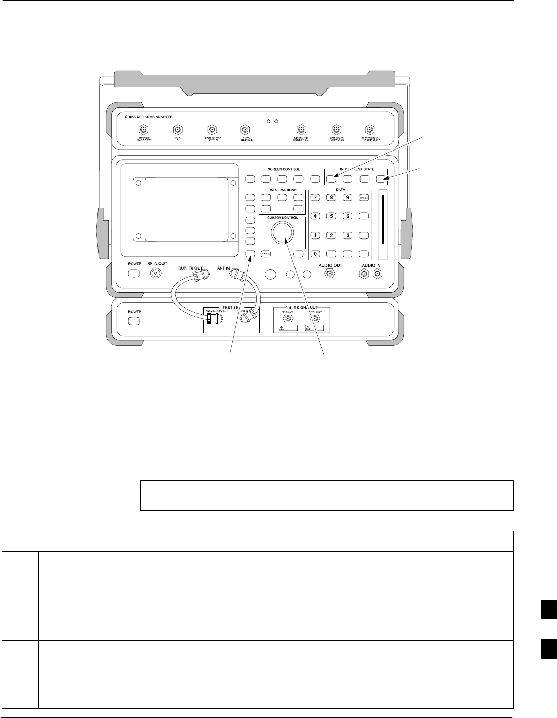
Figure I-3: HP8935 Test Set
FW00885
Preset
Cursor Control
Shift
Inst Config
Local
I

GPIB 68P09255A57-2
Aug 2002
SCt4812ET Optimization/ATP Manual Software Release R16.1.x.x
PRELIMINARY
I-6
Setting HP8921A and HP83236A/B GPIB Address
Follow the procedure in Table I-5 to verify and, if necessary, change the
HP8921A HP83236A GPIB addresses.
NOTE This procedure assumes that the test equipment is set up and
ready for testing.
Table I-5: Verify and/or Change HP8921A and HP83236A GPIB Addresses
Step Action
1To verify that the GPIB addresses are set correctly, press Shift and LOCAL on the HP8921A (see
Figure I-4). The current HP-IB address is displayed at the top of the screen.
NOTE
HP-IB is the same as GPIB.
2If the current HP-IB address is not set to 18, perform the following to change it:
- Turn the Cursor Control knob to move the cursor to More and press the knob to select the field.
- Turn the Cursor Control knob to move the cursor to I/O Config and press the knob to select the
field.
- Turn the Cursor Control knob to move the cursor to Adrs and press the knob to select the field.
- Turn the Cursor Control knob to change the HP-IB address to 18 and press the knob to set the
address.
- Press Shift and Preset to return to normal operation.
3To set the HP83236A (or B) PCS Interface GPIB address=19, set the dip switches as follows:
- A1=1, A2=1, A3=0, A4=0, A5=1, HP-IB/Ser = 1
I
GPIB68P09255A57-2
Aug 2002 SCt4812ET Optimization/ATP Manual Software Release R16.1.x.x
PRELIMINARY
I-7
Figure I-4: HP8921A and HP83236A/B
Preset
Cursor ControlShift
Local
Advantest R3465 GPIB Address
Table I-6 describes the steps to verify and, if necessary, change the GPIB
address for the Advantest R3465.
NOTE This procedure assumes that the test equipment is set up and
ready for testing.
Table I-6: Verify and/or Change Advantest R3465 GPIB Address
Step Action
1To verify that the GPIB address is set correctly, perform the following procedure:
- Press SHIFT then PRESET (see Figure I-5).
- Press LCL.
- Press the GPIB and Others CRT menu key to view the current address.
2If the current GPIB address is not set to 18, perform the following to change it:
- Turn the vernier knob as required to select 18.
- Press the vernier knob to set the address.
3To return to normal operation, press Shift and Preset.
I
GPIB 68P09255A57-2
Aug 2002
SCt4812ET Optimization/ATP Manual Software Release R16.1.x.x
PRELIMINARY
I-8
Figure I-5: R3465 Communications Test Set
BNC
“T”
REF UNLOCK EVEN
SEC/SYNC IN CDMA
TIME BASE IN
POWER
OFF ON
REF FW00337
LCL Shift Preset
GPIB and others
Vernier
Knob
RS232 GPIB Interface Box
Ensure that the RS232 GPIB interface box dip switches are set as shown
in Figure I-6.
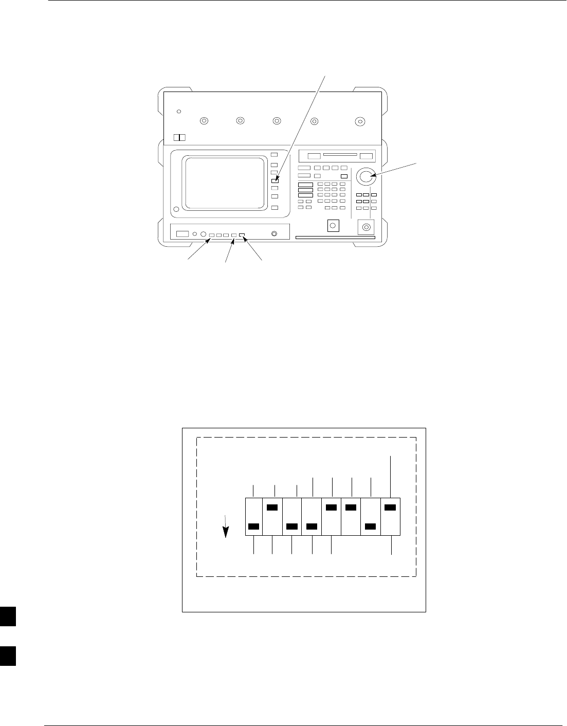
Figure I-6: RS232 GPIB Interface Box
RS232-GPIB
INTERFACE BOX
S MODE
DATA FORMAT
BAUD RATE
GPIB ADRS
ON
DIP SWITCH SETTINGS
G MODE
Advantest R3267 Spectrum Analyzer GPIB Address
Perform the procedure in Table I-7 and refer to Figure I-7 to verify and,
if necessary, change the Advantest R3267 spectrum analyzer GPIB
address.
I
GPIB68P09255A57-2
Aug 2002 SCt4812ET Optimization/ATP Manual Software Release R16.1.x.x
PRELIMINARY
I-9
Table I-7: Verify and Change Advantest R3267 GPIB Address
Step Action
1If the REMOTE LED is lighted, press the LCL key.
- The LED turns off.
2Press the CONFIG key.
- The CONFIG softkey labels will appear in the softkey label display area of the instrument
display.
- The current GPIB address will be displayed below the GPIB Address softkey label.
3
3a
If the current GPIB address is not set to 18, perform the following to change it:
- Press the GPIB Address softkey.
-- A GPIB Address entry window will open in the instrument display showing the current
GPIB address.
3b - Enter 18 on the keypad in the ENTRY section of the instrument front panel.
-- Characters typed on the keypad will replace the address displayed in the GPIB Address
entry window.
NOTE
To correct an entry, press the BS (backspace) key at the lower right of the keypad to delete one
character at a time.
3c - Press the ENTR key to the lower right of the keypad to enter the address.
-- The GPIB Address entry window closes.
-- The new address is diplayed in the bottom portion of the GPIB Address softkey label.
Figure I-7: Setting Advantest R3267 GPIB Address
onREMOTE
LED
LCL Key
CONFIG
Key
Softkey Lable
Display Area Softkey
Buttons
Keypad BS
Key ENTR
Key
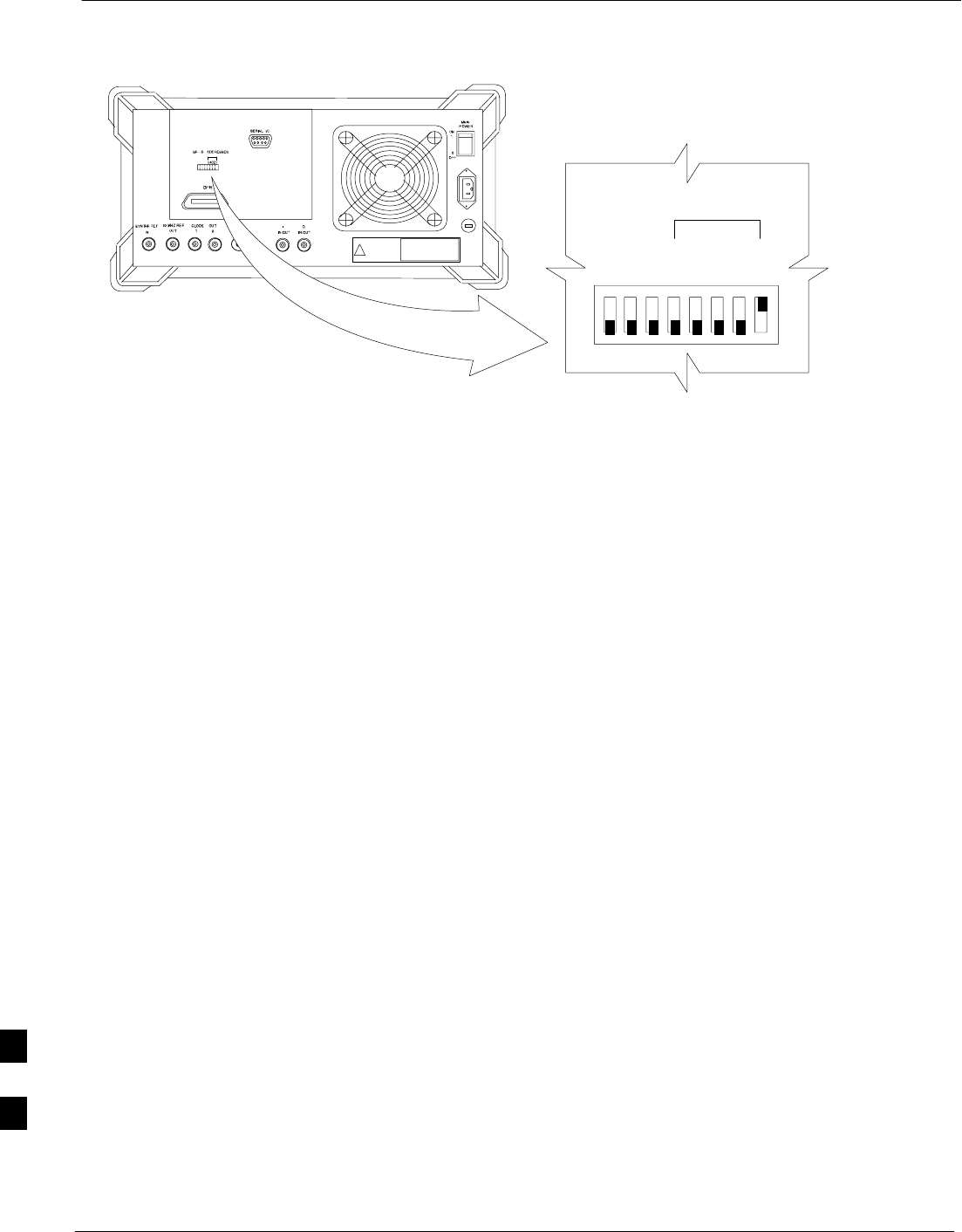
Advantest R3562 Signal Generator GPIB Address
Set the GP-IB ADDRESS switch on the rear of the Advantest R3562
signal generator to address 1 as shown in Figure I-8.
I
GPIB 68P09255A57-2
Aug 2002
SCt4812ET Optimization/ATP Manual Software Release R16.1.x.x
PRELIMINARY
I-10
Figure I-8: Advantest R3562 GPIB Address Switch Setting
12345678
54321
GP-IP ADDRESS
1
0
GPIB Address set to “1”
I

GPIB68P09255A57-2
Aug 2002 SCt4812ET Optimization/ATP Manual Software Release R16.1.x.x
PRELIMINARY
I-11
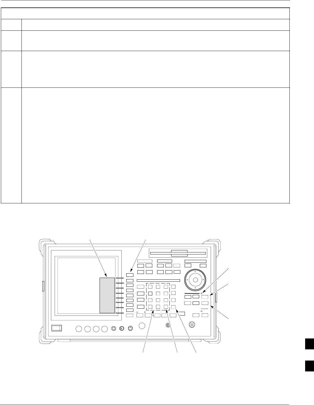
Agilent E4406A Transmitter Tester GPIB Address
Follow the procedure in Table I-8 and refer to Figure I-9 to verify and, if
necessary, change the Agilent E4406A GPIB address.
Table I-8: Verify and Change Agilent E4406A GPIB Address
Step Action
1In the SYSTEM section of the instrument front panel, press the System key.
- The softkey labels displayed on the right side of the instrument screen will change.
2Press the Config I/O softkey button to the right of the instrument screen.
- The softkey labels will change.
- The current instrument GPIB address will be displayed below the GPIB Address softkey label.
3If the current GPIB address is not set to 18, perform the following to change it:
3a - Press the GPIB Address softkey button.
-- In the on-screen Active Function Area, GPIB Address will be displayed followed by the
current GPIB address.
3b - On the front panel Data Entry keypad, enter the communications system analyzer GPIB address of
18.
-- The GPIB Address label will change to Enter.
-- Digits entered with the keypad will replace the current GPIB address in the display.
NOTE
To correct an entry, press the Bk Sp key at the upper right of the keypad to delete one character at a
time.
3c - Press the Enter softkey button or the keypad Enter key to set the new GPIB address.
-- The Config I/O softkey labels will reappear.
-- The new GPIB address will be displayed under the GPIB Address softkey label.
I
GPIB 68P09255A57-2
Aug 2002
SCt4812ET Optimization/ATP Manual Software Release R16.1.x.x
PRELIMINARY
I-12
Figure I-9: Setting Agilent E4406A GPIB Address
System
Key Bk Sp
Key
Enter
Key
Data Entry
Keypad
Softkey
Buttons
Softkey Label
Display Area
Active Function
Area
Agilent E4432B Signal Generator GPIB Address
Follow the procedure in Table I-9 and refer to Figure I-10 to verify and,
if necessary, change the Agilent E4432B GPIB address.
Table I-9: Verify and Change Agilent E4432B GPIB Address
Step Action
1In the MENUS section of the instrument front panel, press the Utility key.
- The softkey labels displayed on the right side of the instrument screen will change.
2Press the GPIB/RS232 softkey button to the right of the instrument screen.
- The softkey labels will change.
- The current instrument GPIB address will be displayed below the GPIB Address softkey label.
3If the current GPIB address is not set to 1, perform the following to change it:
3a - Press the GPIB Address softkey button.
-- The GPIB Address label and current GPIB address will change to boldface.
-- In the on-screen Active Entry Area, Address: will be displayed followed by the current
GPIB address.
. . . continued on next page
I
GPIB68P09255A57-2
Aug 2002 SCt4812ET Optimization/ATP Manual Software Release R16.1.x.x
PRELIMINARY
I-13
Table I-9: Verify and Change Agilent E4432B GPIB Address
Step Action
3b - On the front panel Numeric keypad, enter the signal generator GPIB address of 1.
-- The GPIB Address label will change to Enter.
-- Digits entered with the keypad will replace the current GPIB address in the Active Entry
display.
NOTE
To correct an entry, press the backspace key at the lower right of the keypad to delete one character at
a time.
3c - Press the Enter softkey button to set the new GPIB address.
-- The new GPIB address will be displayed under the GPIB Address softkey label.
Figure I-10: Setting Agilent E4432B GPIB Address
Numeric
Keypad
Softkey
Buttons
Softkey Label
Display Area
Active Entry
Area
Backspace
Key
Utility
Key
I

GPIB 68P09255A57-2
Aug 2002
SCt4812ET Optimization/ATP Manual Software Release R16.1.x.x
PRELIMINARY
I-14
Notes
I

Aug 2002 SCt4812ET Optimization/ATP Manual Software Release R16.1.x.x
PRELIMINARY
J-1
Appendix J
Downloading ROM
J

Downloading ROM Code 68P09255A57-2
Aug 2002
SCt4812ET Optimization/ATP Manual Software Release R16.1.x.x
PRELIMINARY
J-2
Downloading ROM Code
Exception Procedure - Downloading ROM Code
This procedure is not part of a normal optimization.
Perform this procedure only on an exception basis when no alternative
exists to load a BTS device with the correct version of ROM code.
NOTE One GLI must be INS_ACT (bright green) before ROM code
can be downloaded to non-GLI devices.
CAUTION The correct ROM and RAM codes for the software release used
on the BSS must be loaded into BTS devices. To identify the
correct device ROM and RAM code loads for the software
release being used on the BSS, refer to the Version Matrix
section of the SCt CDMA Release Notes (supplied on the tape
or CD-ROM containing the BSS software).
All devices in a BTS must be loaded with the ROM and RAM
code specified for the software release used on the BSS before
any optimization or ATP procedures can be performed.
If a replacement device is loaded with ROM code which is not
compatible with the BSS software release being used, the device
ROM code can be changed using the LMF before performing the
BTS optimization and ATPs. A device loaded with later release
ROM code can not be converted back to a previous release ROM
code in the field without Motorola assistance
If it is necessary to download ROM code to a device from the LMF, the
procedure in Table J-1 includes steps for both ROM and RAM code
download using LMF.
Prerequisites
Prior to performing this procedure, ensure the correct ROM and RAM
code files exist in the LMF computer’s applicable lmf home directory
code folder for each of the devices to be loaded.
CAUTION The Release level of the ROM code to be downloaded must be
the one specified for the software release installed in the BSS.
The release level of the ROM code resident in the other devices
in the BTS must also be correct for the BSS software release
being used. ROM code must not be downloaded to a frame
loaded with code for a BSS software release with which it is not
compatible.
This procedure should only be used to upgrade replacement
devices for a BTS. It should NOT be used to upgrade all devices
in a BTS. If a BTS is to be upgraded from R15.x to R16.0, the
upgrade should be done by the OMC-R using the DownLoad
Manager.
J

Downloading ROM Code68P09255A57-2
Aug 2002 SCt4812ET Optimization/ATP Manual Software Release R16.1.x.x
PRELIMINARY
J-3
Table J-1: Download ROM and RAM Code to Devices
Step Action
1Click on the device to be loaded.
NOTE
More than one device of the same type can be selected for download by either clicking on each one to
be downloaded or from the BTS menu bar Select pull-down menu, select the device item that applies.
Where: device = the type of device to be loaded (BBX, CSM, MCC)
2From the BTS menu bar Device pull-down menu, select Status.
- A status report window will appear.
3Make a note of the number in the HW Bin Type column.
NOTE
“HW Bin Type” is the Hardware Binary Type for the device. This code is used as the last four digits in
the filename of a device’s binary ROM code file. Using this part of the filename, the ROM code file
can be matched to the device in which it is to be loaded.
4 Click OK to close the status window.
5Click on the device to be loaded.
6* IMPORTANT
The LMF will not automatically select ROM code files for download. ROM code files must be
selected manually.
From the BTS menu bar Device pull-down menus, select Download > Code Manual.
- A file selection window will appear.
7Double-click on the version folder with the desired version number for the ROM code file (for
example 2.16.0.x).
8Double-click the Code folder.
- A list of ROM and RAM code files will be displayed.
! CAUTION
A ROM code file with the correct HW Bin Type must be chosen. Using a file with the wrong HW Bin
Type can result in unpredictable operation and damage to the device.
9Click on the ROM code file with the filename which matches the device type and HW Bin Type
number noted in step 3 (for example, file bbx_rom.bin.0604 is the ROM code file for a BBX with a
HW Bin Type of 0604).
- The file should be highlighted.
10 Click on the Load button.
- A status report window is displayed showing the result of the download.
NOTE
If the ROM load failed for some devices, load them individually by clicking on one device, perform
steps 6 through 10 for it, and repeat the process for each remaining device.
11 Click OK to close the status window.
12 From the LMF window menu bar Tools pull-down menus, select Update NextLoad > CDMA.
13 In the left-hand pane of the window which opens, click on the BTS number for the frame being loaded
(for example, BTS-14 ).
. . . continued on next page
J

Downloading ROM Code 68P09255A57-2
Aug 2002
SCt4812ET Optimization/ATP Manual Software Release R16.1.x.x
PRELIMINARY
J-4
Table J-1: Download ROM and RAM Code to Devices
Step Action
14 On the list of versions displayed in the right-hand pane, click the button next to the version number of
the folder that was used for the ROM code download (for example, 2.16.0.x) and click Save.
- A pop-up message will appear showing the CDF has been updated.
15 Click on the OK button to dismiss the pop-up message.
16 Click on the device that was loaded with ROM code.
NOTE
RAM code is automatically selected for download.
17 From the BTS menu bar Device pull-down menus, select Download > Code/Data to download RAM
code and dds file data.
- A status report is displayed showing the result of the download.
18 Click OK to close the status window.
19 Observe the downloaded non-GLI device to ensure it is OOS_RAM (yellow).
20 Click on the device which was loaded with code.
21 From the BTS menu bar Device pull-down menu, select Status.
Verify that the correct ROM and RAM version numbers are displayed in the status report window.
22 Click OK to close the status window.
J

Aug 2002 SCt4812ET Optimization/ATP Manual Software Release R16.1.x.x
PRELIMINARY
K-1
Appendix K
Companion Frame Optimization
K
Optimizing the Companion Frame 68P09255A57-2
Aug 2002
SCt4812ET Optimization/ATP Manual Software Release R16.1.x.x
PRELIMINARY
K-2
Optimizing the Companion Frame
Optimizing the TX section
The optimization/ATP procedure for the transmit side of the Companion
Frame is identical to that of the SC4812ET BTS.
Table K-1: Optimizing the TX section of the Companion Frame
nStep Action
1Please refer to the TX Optimization/ATP - Chapter 3 of this manual for step-by-step TX
Optimization/ATP instructions for the standalone frame
2Run the TX tests.
SC4812ET Companion
C1 C2
C3 C4
RX
TX1
S
S
RX
TX2
RX
TX3
MPC-A
EMPC-B
1 A
2 A
3 A
RX1A
RX3A
RX2A
RX1A
RX2A
RX3A
Ant-1A
1 B
2 B
3 B
Ant-2A
Ant-3A
Figure K-1: Cabling of SC 4812ET Companion BTS to SC 4812ET Companion BTS (3 Sector)
C1 C2
C3 C4
C1 C2
C3 C4
FW00407
SC4812ET Companion
RX
TX1
S
S
RX
TX2
RX
TX3
MPC-A
EMPC-B
RX1A
RX3A
RX2A
RX1A
RX2A
RX3A
Ant-1A
Ant-2A
Ant-3A
C5
C6 C7
C8
RX EXPANSION
1 A
2 A
3 A
1 B
2 B
3 B
SURGE
ARRESTORS
(Starter)
C5
C6 C7
C8
C5
C6 C7
C8
K

Optimizing the Companion Frame68P09255A57-2
Aug 2002 SCt4812ET Optimization/ATP Manual Software Release R16.1.x.x
PRELIMINARY
K-3
Optimizing the RX section
RX (Main) Optimization/ATP
To test the RX Main antenna system follow the instructions in Table K-2
and refer to illustration Figure K-1(3-sector configuration).
Table K-2: Optimizing the RX (Main) section of the Companion Frame
nStep Action
1Connect the RX test cables to the antenna ports 1A-3A (for 3-sector optimization) or
antenna ports 1A-6A (for 6-sector optimization).
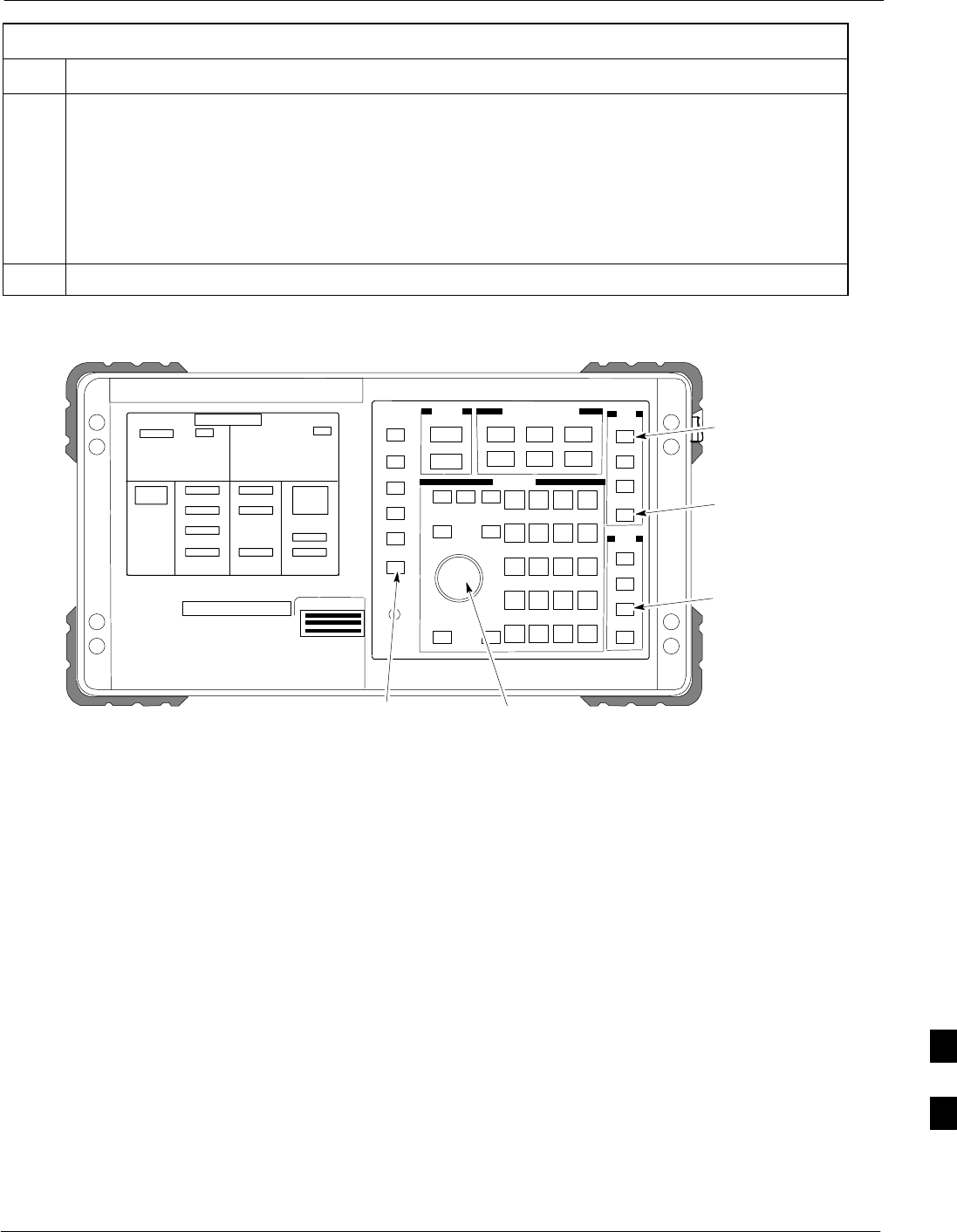
2Login the LMF and select MPC (see Figure K-2 for display screen and field location).
3Run the RX tests.
RX (Diversity) Optimization/ATP (Single Frame)
To test the RX Diversity antenna system follow the instructions in
Table K-3.
Table K-3: Optimizing the RX (Diversity) on a Single Frame
nStep Action
1Connect the RX test cables to the expansion ports on the I/O plates labeled 1B-3B (for
3-sector optimization) or expansion ports 1B-6B (for 6-sector optimization).
2Login the LMF under EMPC (see Figure K-2 for display screen and field location).
3Run the RX tests.
RX (Diversity) Optimization/ATP (Two Frame)
To test the RX Diversity antenna configuration on a two frame
Companion BTS system follow the instructions in Table K-4.
Table K-4: Optimizing the RX (Diversity) on a Two Frame Companion Site
nStep Action
1Connect RX expansion cables from the expansion ports on the other Companion frame
labeled 1A-3A (for 3-sector optimization) or expansion ports 1A-6A (for 6-sector
optimization) to the 1B-3B (for 3-sector optimization) or expansion ports 1B-6B (for
6-sector optimization) see Figure K-1 for an illustration of the configuration.
NOTE
Connect the cables from the 2nd frame A ports to the B ports of the 1st frame.
2Login using the LMF select MPC (see Figure K-2 for field location on LMF display screen)
NOTE
- Although the test will be done to one frame, the RX cable will be connected to the
other frame’s corresponding antenna ports.
- The other frame has to be powered up and include all the RX Path Components.
K
Optimizing the Companion Frame 68P09255A57-2
Aug 2002
SCt4812ET Optimization/ATP Manual Software Release R16.1.x.x
PRELIMINARY
K-4
Figure K-2: WinLMF Display Screen
K

PRELIMINARY
Aug 2002 SCt4812ET Optimization/ATP Manual Software Release R16.1.x.x Index-1
Index

Index 68P09255A57-2
SCt4812ET Optimization/ATP Manual Software Release R16.1.x.x
PRELIMINARY
Aug 2002
Index-2
Numbers
10BaseT/10Base2 Converter, 1-12
2-way Splitter, 1-15
3-Sector Duplexed Directional Coupler to RFDS
Cabling Table, H-23
4812ET RF Cabinet Internal FRU Locations, H-4
6-Sector Duplexed Directional Coupler to RFDS
Cabling Table, H-24
A
Acceptance Test Procedures ATP , 1-3
Acronyms, 1-16
ACTIVE LED
GLI, 6-41
MCC, 6-44
Advantest R3465, 3-64
GPIB, I-9
Alarm and Span Line Cable Pin/Signal Information,
3-8
ALARM LED, GLI, 6-41
Alarm Monitor window, 3-130
Alarm Reporting Display, 3-130
All Cal/Audit Test, 3-113
All inclusive, TX ATP test outline - CCP shelf 1,
primary, 4-18
All tests fail on a single antenna, Troubleshooting,
RFDS, 6-35
AMR, 1-21
Applying AC Power, 2-6
ATP
generate failure report, 4-17
generate report, 4-17
test matrix/detailed optimization, B-3
ATP - Reduced, 4-3
ATP Report, 4-18
ATP Test Procedure, 4-9
B
Basic Troubleshooting Overview, 6-2
Battery Charge Test (Connected Batteries), 2-12
Battery Discharge Test, 2-12
Bay Level offset calibration failure, 6-10
BBX, gain set point vs SIF output considerations, C-2
BBX2, 1-21
BBX2 Connector, 6-25
BBX2 LED Status Combinations, 6-43
Broad Band Receiver. See BBX
BTS
download, 3-42
Ethernet LAN interconnect diagram, 3-25
LMF connection, 3-12, 3-24
system software download, 3-3
BTS Cabinet, 1-28
BTS directory, create, 3-28
Create CAL File, 3-114
C
C-CCP Backplane, H-7
C-CCP Backplane Troubleshooting, Procedure, 6-26
C-CCP shelf, 1-21
cable calibration, automatic, test set-up, 3-72
Advantest R3267/R3562, 3-72
Advantest R3465, 3-71
Agilent 8935, 3-71
Agilent E4406A/E4432B, 3-72
CyberTest, 3-71
HP 8921A, 3-71
Cables Connection for 10 MHz Signal and GPIB ,
F-4, F-6
Calibrate BLO, 3-98
Calibrating Cables, 3-90
Calibrating Test Cable Setup, PCS Interface
HP83236B, F-16
Calibrating Test Equipment, 3-89
Calibration
data file calibration, BLO, 3-100
In-Service, G-18
power meter, Gigatronics 8542B, F-25
Calibration Audit failure, 6-11
calibration data file, description of, BLO, 3-100
Cannot communicate to Communications Analyzer,
6-5
Cannot communicate to Power Meter, 6-4
Cannot Download DATA to any device card, 6-6, 6-7
Cannot ENABLE device, 6-8
Cannot Log into cell-site, 6-3

Index
68P09255A57-2
PRELIMINARY
Aug 2002 SCt4812ET Optimization/ATP Manual Software Release R16.1.x.x Index-3
Cannot perform carrier measurement, 6-16
Cannot perform Code Domain Noise Power
measurement, 6-15
Cannot perform Rho or pilot time offset
measurement, 6-14
Cannot perform Txmask measurement, 6-13
CCD, 1-21
CCP, shelf 1 - all inclusive TX ATP test outline,
primary, 4-18
CDF
site configuration, 3-3
site equipage verification, 3-4
site type and equipage data information, 2-2
CDF file
create, 3-31
update device load version, 3-32, 3-33
CDMA
allocation diagram for the North American, cellular
telephone frequency spectrum, D-6
optimization/ATP test matrix, B-2
cdpower test, 4-14
Cell Site
equipage verification, 2-2
types configuration, 3-3
Cell Site Data File. See CDF
Cell Site Field Engineer CFE, 1-3
Channel Service Unit, 3-6
CIO, 1-21
CIO Connectors, 6-25
CLI, 1-4
Clock Sync Module. See CSM
Code Domain Power and Noise Floor Levels, 4-15
Code Domain Power/Noise, 4-14
Communication test set, rear panel, F-4, F-6
Communications System Analyzer, 1-13
Communications system analyzer , 1-13
Components Located on CIO Card, H-11
Connecting test equipment to the BTS, 3-62
Connector Functionality
Backplane, Troubleshooting, 6-24
Troubleshooting, Backplane, 6-24
Copy CAL Files From Diskette to the CBSC, 5-4
Copy CDF Files from CBSC, 3-19
Copy Files from LMF to Diskette, 5-4
Copying CAL files from CDMA LMF to the CBSC,
5-4
Copying CAL files to the CBSC, 5-4
create
BTS directory, 3-28
CDF file, 3-31
master-bts-cdma, 3-28
CSM, 1-21
and LFR primary functions, 3-52
CSM frequency verification, 3-54
CSM LED Status Combinations, 6-39
Customer I/O, 1-21
CyberTest, 3-64
CyberTest Communication Analyzer, 1-13
D
DC Power Pre-test (BTS Frame), 2-8
DC Power Problems, C-CCP Backplane
Troubleshooting, 6-30
DC/DC Converter LED Status Combinations, 6-38
Detailed, optimization/ATP test matrix, B-3
Devices, download. See Download
Digital Control Problems, 6-27
C-CCP Backplane Troubleshooting, 6-27
Digital Multimeter, 1-14
Directional Coupler, 1-14
Download
See also Devices
BTS, 3-42
BTS system software, 3-3
Download BLO Procedure, 3-106
download ROM and RAM code. See ROM code
Download/Enable MCCs, 3-51
Download/Enable MGLIs, 3-45
Duplexer/Directional Coupler DDC, 1-20, 1-21, 1-22,
1-30
E
Enable CSMs & BDCs, 3-49
Equipment Overview, 1-18
Equipment warm-up, 3-68
Ethernet LAN
interconnect diagram, 3-25
transceiver, 1-12
ETIB I/O Connectors, H-13

Index 68P09255A57-2
SCt4812ET Optimization/ATP Manual Software Release R16.1.x.x
PRELIMINARY
Aug 2002
Index-4
Every test fails, Troubleshooting, RFDS, 6-33
F
fer test, 4-16
Files, calibration data file, BLO, 3-100
Folder Structure Overview, 3-21, 3-23
Foreword, xx
FREQ Monitor Connector, CSM, 6-40
Frequency counter, optional test equipment, 1-15
G
Gain set point, C-2
General Safety, xxii
General optimization checklist, test data sheets, A-6
Gigatronics 8542B power meter, illustration, F-25,
I-4
Gigatronics Power Meter, 3-64
GLI. See Master (MGLI2) and Slave (SGLI2) Group
Line Interface
GLI Connector, 6-25
GLI Ethernet A and B Connections, 6-25
GLI LED Status Combinations, 6-41
GLI Pushbuttons and Connectors, 6-42
GLI2, 1-21
GLI2 Front Panel Operating Indicators, 6-42
GPIB, F-3, F-7, F-11
Advantest R3465, I-9
HP83236A/B, I-7
HP8921A, I-7
HP8935, I-6
power meter
Gigatronics 8542B, I-4
HP437B, I-3
set address, Motorola CyberTest, I-5
GPIB Cables, 1-13
GPS, receiver operation, test data sheets, A-7
GPS Initialization/Verification
estimated position accuracy, 3-55
surveyed position accuracy, 3-55
GPS satellite system, 3-49
Graphical User Interface Overview , 3-34, 3-35
Group Line Interface. See GLI
H
Hardware Requirements, 1-9
High Stability 10 MHz Rubidium Standard, 1-15
High-impedance Conductive Wrist Strap, 1-14
HP 437B, 3-64
HP 83236A, F-7
HP 8921, 3-64
HP83236A/B, GPIB, I-7
HP8921A, F-7
GPIB, I-7
HP8935, GPIB, I-6
HP8935 Analyzer, 1-13
HSO, 1-21
HSO Initialization/Verification, 3-53
I
I and Q values, E-3
In-Service Calibration, G-18
Initial HP8921A setup, F-16
Initial Installation of Boards/Modules, preliminary
operations, 2-2
Initial power tests, test data sheets, A-5
Installation and Update Procedures, 3-16
Intercabinet I/O, 1-22
Internal FRU, 1-29
Internal FRUs, 1-20
IS-97 specification, E-3
ISB Inter Shelf Bus connectors, 6-24
L
LAN, BTS frame interconnect, illustration, 3-25

Index
68P09255A57-2
PRELIMINARY
Aug 2002 SCt4812ET Optimization/ATP Manual Software Release R16.1.x.x Index-5
LED Status Combinations for all Modules except
GLI2 CSM BBX2 MCC24 MCC8E, 6-37
LFR, 1-21
receiver operation, test data sheets, A-8
Line Build Out parameters
configure, 5-8
verify, 5-6
LMF, F-3, F-11
to BTS connection, 3-12, 3-24
view CDF information, 3-4
LMF Removal, 5-12
Load Center Wiring, 2-5
Local Area Network (LAN) Tester, 1-15
Log into the BTS, 3-27
Log into the LMF, 3-27
Logging In to a BTS, 3-36
Logging Out, 3-39
LORAN-C Initialization/Verification, 3-60
LPA errors, 6-9
LPA Module LED, 6-45
LPA Shelf LED Status Combinations, 6-45
LPAC Interface Board, H-12
M
major components, 1-19
Manual, layout, 1-2
Master Group Line Interface. See MGLI
MASTER LED, GLI, 6-41
master-bts-cdma directory, create, 3-28
MCC LED Status Combinations, 6-44
MCC/CE, 4-14
MGLI2, board detail, MMI port connections, 5-7
MMI common connections, 3-41
MMI Connection, 3-41
MMI Connector
CSM, 6-40
GLI, 6-42
MMI Connectors, MCC, 6-44
MMI equipment setup, 3-41
Model SLN2006A MMI Interface Kit, 1-13
Module status indicators, 6-36
Motorola, SC9600 Base Transceiver Subsystem, 1-2
MPC, 1-21
Multi Channel Card. See MCC
Multi-FER test Failure, 6-17
N
New Installations, 1-6
No AMR control, 6-28
No BBX2 control in the shelf, 6-28
No DC input voltage to Power Supply Module, 6-30
No DC voltage +5 +65 or +15 Volts to a specific
GLI2 BBX2 or Switch board, 6-31
No GLI2 Control through span line connection, 6-27
No GLI2 Control via LMF, 6-27
No or missing MCC24 channel elements, 6-29
No or missing span line traffic, 6-28
North American, cellular telephone system frequency
spectrum, CDMA allocation, D-6
Null modem cable detail, 1-12
O
Online Help, 1-4
Optimization, 1-3
optimization/ATP, test set-up, 3-76
Advantest R3267/R3562
DRDCs, 3-79
TRDCs, 3-81
Advantest R3465, 3-76
Agilent 8935
DRDCs, 3-78
TRDCs, 3-80
Agilent E4406A/E4432B
DRDCs, 3-78
TRDCs, 3-80
CyberTest, 3-76
HP 8921A, 800 MHz, 3-77
HP 8921A, 1.9 GHz, 3-77
Optimization/ATP Test Matrix, 1-6
Optional Test Equipment, 1-15
Optional test equipment, frequency counter, 1-15
Oscilloscope, 1-15
P
Pilot Time Offset. See PN
Ping, 3-25

Index 68P09255A57-2
SCt4812ET Optimization/ATP Manual Software Release R16.1.x.x
PRELIMINARY
Aug 2002
Index-6
PN
offset programming information, E-2
offset usage, E-3
PN offset per sector, E-3
PN Offset Usage , E-3
Power Delta Calibration
Advantest, G-7
HP8921A, G-4
HP8935, G-10
Power Input, 6-24
Power Meter, 1-13
illustration, F-23, I-3
Pre-calibration, F-23
Power meter
calibration, Gigatronics 8542B, F-25
GPIB
Gigatronics 8542B, I-4
HP437B, I-3
illustration, Gigatronics 8542B, F-25, I-4
Power Supply Module Interface, 6-24
Pre-calibration, Power Meter, F-23
Pre-power tests, test data sheets, A-5
Preliminary operations
cell Site types, 2-2
test data sheets, A-4
Prepare to Leave the Site
External test equipment removal, 5-2
LMF Removal, 5-12
Reestablish OMC-R control, 5-13
Verify T1/E1, 5-13
Prepare to leave the site
re-connect BTS IFM connector, 5-11
re-connect BTS T1 spans, 5-11
Procedures to Copy CAL Files From Diskette to the
CBSC, 6-3, 6-4, 6-5, 6-6, 6-7
Product Description, 1-4
Pseudorandom Noise. See PN
ptoff test, 4-13
Punch Block, 3-8
PWR/ALM and ACTIVE LEDs, MCC, 6-44
PWR/ALM LED
BBX2, 6-43
CSM, 6-39
DC/DC Converter, 6-38
generic, 6-37
MCC, 6-44
MPC and EMPC Card, H-21
R
RAM code, described, 3-42
Re-connect BTS IFM connector, 5-11
Re-connect BTS T1 Spans, 5-11
Receive Distribution Card RXDC, 1-30
Reduced ATP, 4-3
Reduced ATP passes but forward link problem
prevails, 6-12
Reestablish OMC-R control, 5-13
Removing and Installing LPAs for the SC 4812ET,
H-8
Required documents, 1-7, 1-29
Required Test Equipment
Ethernet LAN transceiver, 1-12
substitute equipment, 1-8
RESET Pushbutton, GLI, 6-42
Resetting BTS modules, 5-3
Revision History, xxiv
RF Adapters, 1-14
RF Attenuators, 1-14
50 Pair Punchblock, H-27
RF Path Bay Level Offset Calibration, 3-97
RF Test Cable, 1-15
RFDS Cabling Details, H-23
RFDS calibration
description, 3-125
procedure, 3-126
RFDS FRU, H-15
RFDS Location, SC 4812ET, 1-24
RFDS parameters, 3-116
checking, 3-117
setting, 3-117
RFDS Test Subscriber Unit, 3-43
RFDS TSU Calibration Channel Frequencies, 3-125
rho test, 4-12
ROM code
described, 3-42
downloading, J-2, K-2, K-3
procedure, J-3

Index
68P09255A57-2
PRELIMINARY
Aug 2002 SCt4812ET Optimization/ATP Manual Software Release R16.1.x.x Index-7
RS-232 to GPIB Interface, 1-12
Rubidium Standard Timebase, 3-64
RX, antenna VSWR, test data sheets, A-18
RX and TX paths fail, Troubleshooting, RFDS, 6-34
S
SC 4812 BTS Optimization/ATP Test Matrix, B-4
SC 4812ET BTS Combiner, H-9, H-10, H-17, H-18,
H-19, H-20, H-22, H-23, H-25
SCLPA, convergence test data sheets, A-9
Selecting Test Equipment, 3-85
Set Antenna Map Data, 3-123
Set RFDS Configuration Data, 3-124
Set Span Parameter Configuration, procedure, 5-8
Setting Cable Loss Values, 3-94
Setting Control Port, 3-6
Setting Coupler Loss Value, 3-95
SGLI2, board detail, MMI port connections, 5-7
SIF, output considerations vs BBX gain set point, C-2
Site, equipage verification, 3-4
Site checklist, verification data sheets, A-3
site equippage, CDF file, 3-3
Site Specific BTS Files, 3-28
Span Framing Format
configure, 5-8
verify, 5-6
SPAN I/O Functional Description, Introduction, H-14
Span Line (T1/E1) Verification Equipment, 1-15
Span Line connector , 6-24
Span Parameter Configuration
set, procedure, 5-8
verification, procedure, 5-6
Span Problems no control link, Troubleshooting, 6-46
SPANS LED, 6-41
Spectrum Analyzer, 1-15
Spectrum Analyzer , HP8594E, 3-64
STATUS LED, GLI, 6-41
SYNC Monitor Connector, CSM, 6-40
System Connectivity Test, F-7
T
T1, isolate BTS from the T1 spans, 3-5, 3-14
Telco Interface Board TIB, 1-30
Test data sheets
Alarm verification, A-19
general optimization checklist, A-6
GPS receiver operation, A-7
initial power tests, A-5
LFR receiver operation, A-8
pre-power tests, A-5
preliminary operations, A-4
RX antenna VSWR, A-18
SCLPA convergence, A-9
site checklist, A-3
TX antenna VSWR, A-16
TX BLO, A-10, A-15
verification of test equipment used, A-2
Test equipment, verification data sheets, A-2
Test equipment connections , F-3
preliminary Agilent E4406A/E4432B set-up, F-15
Test Equipment Policy, 1-8
Test Equipment Setup Calibration for TX Bay Level
Offset, 3-93, F-20
Test Equipment Setup Chart, 3-66
Test equipment setup RF path calibration, 3-103
Timing Reference Cables, 1-13
Transmit TX path audit, 3-109
Transmit TX path calibration, 3-104
Transmit/Receive Module TRX, 1-29
Troubleshooting
DC Power Problems, 6-30
Span Problems no control link, 6-46
Troubleshooting Forward Link Failure (BTS Passed
Reduced ATP), 6-12
TSU NAM, programming
description, 3-120
parameter ranges, 3-122
parameters, 3-121
procedure, 3-128
TX
antenna VSWR, test data sheets, A-16, A-19
BLO test data sheets, A-10, A-15
TX and RX Frequency vs Channel , D-4
TX Audit Test, 3-110
TX Bay Level Offset and TX ATP test equipment
setup calibration, 3-92

Index 68P09255A57-2
SCt4812ET Optimization/ATP Manual Software Release R16.1.x.x
PRELIMINARY
Aug 2002
Index-8
TX calibration, set-up, 3-73
Advantest R3267, 3-75
Advantest R3465, 3-74
Agilent 8935, 3-73
Agilent E4406A, 3-75
CyberTest, 3-73
HP 8921A, 3-74
tx fine adjust, E-3
TX Mask Verification, spectrum analyzer display,
illustration, 4-11
TX Output Acceptance Tests - Introduction
Code domain power, 4-8
Pilot time offset, 4-8
Spectral purity TX mask, 4-8
Waveform Quality (rho), 4-8
TX Path Calibration, 3-99
TX/RX OUT Connections, 4-5
txmask test, 4-10
U
Updating CDMA LMF Files, 5-4
V
Verify, test equipment used, test data sheets, A-2
Verify GLI ROM code load, 3-44
Verify Span Parameter Configuration, procedure, 5-6
W
Walsh channels, 4-14
X
XCVR Backplane Troubleshooting, 6-24
Xircom Model PE3-10B2, LMF to BTS connection,
3-24