Nokia Solutions and Networks T5JX1 UBS CDMA XMI Transceiver at 800 MHz User Manual Exhibit 8b
Nokia Solutions and Networks UBS CDMA XMI Transceiver at 800 MHz Exhibit 8b
Contents
Exhibit 8b

APPLICANT: MOTOROLA
Cellular Networks
FCC ID: IHET5JX1
FRU Manual Exhibit
UBS CDMA XMI Transceiver at 800MHz
FCC Filing – UBS CDMA XMI Transceiver at 800MHz (cover page)

1X UBS Macro BTS FRU
68P09283A64 -3 SEP 2007
FOA
© 2007 Motorola, Inc. All Rights R eserv ed

Accuracy
While reasonable efforts have been made to assure the accuracy of this document, Motorola, Inc. assumes no
liability resulting from any inaccuracies or omissions in this document, or from use of the information obtained
herein. Motorola, Inc. reserves the right to make changes to any products described herein to improve reliability ,
function, or design, and reserves the right to revise this document and to make changes from time to time in content
hereof with no obligation to notify any person of revisions or changes. Motorola, Inc. does not assume any liability
arising out of the application or use of any product, software, or circuit described herein; neither does it convey
license under its patent rights or the rights of others. It is possible that this publication may contain references to, or
information about Motorola products (machines and programs), programming, or services that are not announced
in your country . Such references or information must not be construed to mean that Motorola intends to announce
such Motorola products, programming, or services in your country .
Copyrights
This document, Motorola products, and 3rd P arty Software products described in this document may include
or describe copyrighted Motorola and other 3rd P arty supplied computer programs stored in semiconductor
memories or other media. Laws in the United States and other countries preserve for Motorola, its licensors, and
other 3rd P arty supplied software certain exclusive rights for copyrighted material, including the exclusive right
to copy , reproduce in any form, distribute and make derivative works of the copyrighted material. Accordingly ,
any copyrighted material of Motorola, its licensors, or the 3rd P arty software supplied material contained in the
Motorola products described in this document may not be copied, reproduced, reverse engineered, distributed,
merged or modified in any manner without the express written permission of Motorola. Furthermore, the purchase
of Motorola products shall not be deemed to grant either directly or by implication, estoppel, or otherwise, any
license under the copyrights, patents or patent applications of Motorola or other 3rd P arty supplied software,
except for the normal non-exclusive, royalty free license to use that arises by operation of law in the sale of a
product.
A list of 3rd P arty supplied software copyrights are contained in the Supplemental information section of this
document.
Restrictions
Software and documentation are copyrighted materials. Making unauthorized copies is prohibited by law . No part
of the software or documentation may be reproduced, transmitted, transcribed, stored in a retrieval system, or
translated into any language or computer language, in any form or by any means, without prior written permission
of Motorola, Inc.
License Agreements
The software described in this document is the property of Motorola, Inc and its licensors. It is furnished by express
license agreement only and may be used only in accordance with the terms of such an agreement.
High Risk Materials
Components, units, or 3rd P arty products used in the product described herein are NOT fault-tolerant and are NOT
designed, manufactured, or intended for use as on-line control equipment in the following hazardous environments
requiring fail-safe controls: the operation of Nuclear F acilities, Aircraft Navigation or Aircraft Communication
Systems, Air Traffic Control, Life Support, or W eapons Systems (High Risk Activities). Motorola and its supplier(s)
specifically disclaim any expressed or implied warranty of fitness for such High Risk Activities.
T rademarks
Motorola and the Stylized M Logo are registered in the US P atent & Trademark Office. All other product or service
names are the property of their respective owners.
The CE mark confirms Motorola, Inc. statement of compliance with EU directives applicable to this product. Copies
of the Declaration of Compliance and installation information in accordance with the requirements of EN50385 can
be obtained from the local Motorola representative or by contacting the Customer Network Resolution Center
(CNRC). The 24 hour telephone numbers are listed at h t t p s : / / m y n e t w o r k s u p p o r t . m o t o r o l a . c o m . Select Customer
Network Resolution Center contact information. Alternatively if you do not have access to CNRC or the
internet, contact the Local Motorola Office.
FOA SEP 2007

T a b l e
o f
C o n t e n t s
Contents
■■■■■■■■■■■■■■■■■■■■■■■■■■■■■■■■■■■■■■■■■■■■■■■■■■■■■■■■■■■■■■
■
■
■
■
1X UBS Macro BTS FRU
Revision history ......................................... 2
Version information ..................................... 2
Resolution of Service Requests . . . . . . . . . . . . . . . . . . . . . . . . . . . . . . . 2
Incorporation of Change Notices . . . . . . . . . . . . . . . . . . . . . . . . . . . . . . . 2
General information ....................................... 3
Purpose ........................................... 3
Cross references ....................................... 3
Text conventions ....................................... 4
Contacting Motorola ....................................... 5
24–hour support ....................................... 5
Questions and comments .................................. 5
Errors ............................................ 5
Security advice .......................................... 6
W arnings, cautions, and notes . . . . . . . . . . . . . . . . . . . . . . . . . . . . . . . . . . 7
W arnings ........................................... 7
Cautions ........................................... 7
Notes ............................................ 7
Safety .............................................. 8
General safety ........................................ 8
Electromagnetic energy ................................... 8
Caring for the environment . . . . . . . . . . . . . . . . . . . . . . . . . . . . . . . . . . . 9
In EU countries ....................................... 9
In non -EU countries ..................................... 9
CMM labeling and disclosure table . . . . . . . . . . . . . . . . . . . . . . . . . . . . . . . 10
Motorola document set ..................................... 11
Ordering documents and CD -ROMs . . . . . . . . . . . . . . . . . . . . . . . . . . . . . 11
Document banner definitions . . . . . . . . . . . . . . . . . . . . . . . . . . . . . . . . 11
Data encryption ....................................... 11
Third P arty Computer Software and Trademarks . . . . . . . . . . . . . . . . . . . . . . . . 12
Computer Software ..................................... 12
Trademarks ......................................... 12
FCC Requirements ........................................ 13
Content ........................................... 13
FCC Part 15 Requirements .................................. 13
Chapter 1: Overview
Information Overview ...................................... 1 - 2
Organization of manual ................................... 1 - 2
How to use this manual ................................... 1 - 5
Required manuals ...................................... 1 - 5
FRU locations ........................................ 1 - 5
68P09283A64 -3 i
SEP 2007 FOA
Contents
Recommended tools ..................................... 1 - 6
Abbreviations and Acronyms . . . . . . . . . . . . . . . . . . . . . . . . . . . . . . . . . 1 - 6
UBS Macro BTS FRU Replacement Preview . . . . . . . . . . . . . . . . . . . . . . . . . . . 1 - 10
Passive and DC operation .................................. 1 - 10
FRU backup ......................................... 1 - 10
Service affecting FRUs .................................... 1 - 10
Shutdown and restore signaling . . . . . . . . . . . . . . . . . . . . . . . . . . . . . . . 1 - 10
T esting/reoptimization . . . . . . . . . . . . . . . . . . . . . . . . . . . . . . . . . . . . 1 - 10
FRU replacement conditions and sequence . . . . . . . . . . . . . . . . . . . . . . . . . 1 - 11
UBS Macro BTS Product Overview . . . . . . . . . . . . . . . . . . . . . . . . . . . . . . . . 1 - 15
Introduction ......................................... 1 - 15
UBS Macro BTS Frame Overview . . . . . . . . . . . . . . . . . . . . . . . . . . . . . . 1 - 15
UBS Macro BTS Frame Standard Equipment . . . . . . . . . . . . . . . . . . . . . . . . 1 - 16
UBS Macro BTS Frame Optional Equipment . . . . . . . . . . . . . . . . . . . . . . . . . 1 - 21
UBS Macro BTS Frame Optional External Equipment . . . . . . . . . . . . . . . . . . . . 1 - 23
UBS Macro BTS FRU List .................................. 1 - 23
UBS Macro BTS Equipment Identification . . . . . . . . . . . . . . . . . . . . . . . . . . . . 1 - 26
Low and mid capacity UBS Macro BTS Frames . . . . . . . . . . . . . . . . . . . . . . . 1 - 26
External GPS (E -GPS) Equipment Identification . . . . . . . . . . . . . . . . . . . . . . . . . 1 - 31
E -GPS I/O Details ...................................... 1 - 31
Integrated Duplexer RX Filter (IDRF) Equipment Identification . . . . . . . . . . . . . . . . . 1 - 32
IDRF I/O Details ....................................... 1 - 32
Site Span I/O (S SI) Module Equipment Identification . . . . . . . . . . . . . . . . . . . . . . 1 - 34
SSI I/O Details ........................................ 1 - 34
Transceiver Module Internal (XMI) Equipment Identification . . . . . . . . . . . . . . . . . . 1 - 37
XMI I/O Details ....................................... 1 - 37
Digital Module Internal (DMI) Equipment Identification . . . . . . . . . . . . . . . . . . . . . 1 - 40
DMI I/O Panel ........................................ 1 - 40
P ower Distribution Unit (PDU) Equipment Identification . . . . . . . . . . . . . . . . . . . . . 1 - 42
PDU I/O Panels ........................................ 1 - 42
RX Splitter Equipment Identification . . . . . . . . . . . . . . . . . . . . . . . . . . . . . . . 1 - 44
RX Splitter I/O Panel ..................................... 1 - 44
P ower Supply Module (PSM) Shelf Equipment Identification . . . . . . . . . . . . . . . . . . 1 - 45
PSM I/O Panels ....................................... 1 - 45
Optional RGPS Head Equipment Identification . . . . . . . . . . . . . . . . . . . . . . . . . . 1 - 49
RGPS Head Mounting Method . . . . . . . . . . . . . . . . . . . . . . . . . . . . . . . . 1 - 49
RGPS Head Details ..................................... 1 - 50
Chapter 2: Reference Procedures Performed At BTS Site
Reference Procedures P erformed at BTS Site . . . . . . . . . . . . . . . . . . . . . . . . . . 2 - 2
Introduction ......................................... 2 - 2
Frame P ower Down & P ower -Up Procedures . . . . . . . . . . . . . . . . . . . . . . . . . . . 2 - 3
P owering Down the Frame . . . . . . . . . . . . . . . . . . . . . . . . . . . . . . . . . . 2 - 3
Power -up the Frame ..................................... 2 - 3
Chapter 3: Reference Procedures Performed At OMCR
Reference procedures performed at OMCR . . . . . . . . . . . . . . . . . . . . . . . . . . . 3 - 2
Introduction ......................................... 3 - 2
Accessing OMCR CLI window . . . . . . . . . . . . . . . . . . . . . . . . . . . . . . . . . . 3 - 3
Accessing OMCR CLI window . . . . . . . . . . . . . . . . . . . . . . . . . . . . . . . . 3 - 3
P acket BTS shutdown procedures . . . . . . . . . . . . . . . . . . . . . . . . . . . . . . . . 3 - 4
Shutdown site signaling functions for a packet BTS . . . . . . . . . . . . . . . . . . . . . 3 - 4
P acket BTS start -up procedures . . . . . . . . . . . . . . . . . . . . . . . . . . . . . . . . . 3 - 10
Restore site signaling operations for a packet BTS . . . . . . . . . . . . . . . . . . . . . . 3 - 10
ii 68P09283A64 -3
FOA SEP 2007
1X UBS Macro B T S FRU Contents
Chapter 4: E -GPS (External -GPS) Replacement Procedures
E -GPS (External -GPS) ...................................... 4 - 2
E -GPS Description ...................................... 4 - 2
System Impact/Considerations . . . . . . . . . . . . . . . . . . . . . . . . . . . . . . . . 4 - 2
Required Items ....................................... 4 - 3
Prerequisite ......................................... 4 - 4
E -GPS Replacement Procedure . . . . . . . . . . . . . . . . . . . . . . . . . . . . . . . 4 - 4
Optimization Required .................................... 4 - 5
Chapter 5: IDRF Replacement Procedure
IDRF (Integrated Duplexer RX Filter) . . . . . . . . . . . . . . . . . . . . . . . . . . . . . . 5 - 2
IDRF Description ...................................... 5 - 2
System Impact/Considerations . . . . . . . . . . . . . . . . . . . . . . . . . . . . . . . . 5 - 2
Required Items ....................................... 5 - 3
Prerequisite ......................................... 5 - 4
IDRF Replacement Procedure . . . . . . . . . . . . . . . . . . . . . . . . . . . . . . . . 5 - 4
Optimization Required .................................... 5 - 5
Chapter 6: SSI Replacement Procedures
S SI (Site Span I/O) Module . . . . . . . . . . . . . . . . . . . . . . . . . . . . . . . . . . . . 6 - 2
SSI Description ....................................... 6 - 2
System impact/considerations . . . . . . . . . . . . . . . . . . . . . . . . . . . . . . . . 6 - 3
SSI LEDs ........................................... 6 - 4
Required items ........................................ 6 - 5
Prerequisite ......................................... 6 - 6
S SI replacement procedure . . . . . . . . . . . . . . . . . . . . . . . . . . . . . . . . . 6 - 6
Optimization Required .................................... 6 - 8
Unbalanced E1 Daughter Card . . . . . . . . . . . . . . . . . . . . . . . . . . . . . . . . . . 6 - 9
Unbalanced E1 Daughter Card Description . . . . . . . . . . . . . . . . . . . . . . . . . 6 - 9
System impact/considerations . . . . . . . . . . . . . . . . . . . . . . . . . . . . . . . . 6 - 9
Required items ........................................ 6 - 10
Prerequisite ......................................... 6 - 10
E1 daughter card replacement procedure . . . . . . . . . . . . . . . . . . . . . . . . . . 6 - 11
QHSO (Quartz High Stability Oscillator) . . . . . . . . . . . . . . . . . . . . . . . . . . . . . 6 - 13
QHSO Description ...................................... 6 - 13
System impact/considerations . . . . . . . . . . . . . . . . . . . . . . . . . . . . . . . . 6 - 13
Required items ........................................ 6 - 14
Prerequisites ......................................... 6 - 14
QHSO replacement procedure . . . . . . . . . . . . . . . . . . . . . . . . . . . . . . . . 6 - 15
Optimization required .................................... 6 - 16
Chapter 7: XMI Replacement Procedures
XMI (Transceiver Module Internal) Module . . . . . . . . . . . . . . . . . . . . . . . . . . . 7 - 2
XMI Description ....................................... 7 - 2
System Impact/Considerations . . . . . . . . . . . . . . . . . . . . . . . . . . . . . . . . 7 - 7
Required items ........................................ 7 - 8
XMI I/O P anel Connectors/P orts & LEDs . . . . . . . . . . . . . . . . . . . . . . . . . . . 7 - 9
XMI “HOT" W arning Label Details . . . . . . . . . . . . . . . . . . . . . . . . . . . . . . 7 - 12
Prerequisites ......................................... 7 - 13
XMI Replacement Procedures . . . . . . . . . . . . . . . . . . . . . . . . . . . . . . . . 7 - 14
XMI Fan Tray Assembly ..................................... 7 - 22
XMI F an Tray Assembly Description . . . . . . . . . . . . . . . . . . . . . . . . . . . . . 7 - 22
System Impact/Considerations . . . . . . . . . . . . . . . . . . . . . . . . . . . . . . . . 7 - 22
XMI Fan Tray Diagrams ................................... 7 - 23
68P09283A64 -3 iii
SEP 2007 FOA
Contents
Required Items ....................................... 7 - 26
Prerequisites ......................................... 7 - 26
XMI F an Tray Assembly Replacement . . . . . . . . . . . . . . . . . . . . . . . . . . . . 7 - 27
Chapter 8: DMI Replacement Procedures
DMI Replacement Procedures . . . . . . . . . . . . . . . . . . . . . . . . . . . . . . . . . . 8 - 2
Introduction ......................................... 8 - 2
DMI (Digital Module Internal) Assembly . . . . . . . . . . . . . . . . . . . . . . . . . . . . . 8 - 3
DMI Description ....................................... 8 - 3
System impact/considerations . . . . . . . . . . . . . . . . . . . . . . . . . . . . . . . . 8 - 5
Required items ........................................ 8 - 5
DMI I/O P anel Connectors/P orts & LEDs . . . . . . . . . . . . . . . . . . . . . . . . . . . 8 - 7
Prerequisites ......................................... 8 - 9
Reference Diagrams ..................................... 8 - 12
DMI Replacement Procedure . . . . . . . . . . . . . . . . . . . . . . . . . . . . . . . . 8 - 14
Optimization Recommended . . . . . . . . . . . . . . . . . . . . . . . . . . . . . . . . . 8 - 17
Dismantling the failed DMI assembly in the Field . . . . . . . . . . . . . . . . . . . . . . 8 - 18
Modem Boards .......................................... 8 - 20
1X Modem Board Description . . . . . . . . . . . . . . . . . . . . . . . . . . . . . . . . 8 - 20
System impact/considerations . . . . . . . . . . . . . . . . . . . . . . . . . . . . . . . . 8 - 21
Required items ........................................ 8 - 22
Prerequisites ......................................... 8 - 22
Modem Board Replacement Procedure . . . . . . . . . . . . . . . . . . . . . . . . . . . 8 - 23
Reference Diagrams ..................................... 8 - 27
Optimization Recommended . . . . . . . . . . . . . . . . . . . . . . . . . . . . . . . . . 8 - 29
Chapter 9: PDU Replacement Procedures
P ower Distribution Unit (PDU) . . . . . . . . . . . . . . . . . . . . . . . . . . . . . . . . . . 9 - 2
PDU Description ....................................... 9 - 2
System impact/considerations . . . . . . . . . . . . . . . . . . . . . . . . . . . . . . . . 9 - 3
Required items ........................................ 9 - 3
Prerequisites ......................................... 9 - 4
PDU replacement procedure . . . . . . . . . . . . . . . . . . . . . . . . . . . . . . . . . 9 - 4
Breaker Module Assembly (BMA) . . . . . . . . . . . . . . . . . . . . . . . . . . . . . . . . 9 - 7
BMA Description ....................................... 9 - 7
System impact/considerations . . . . . . . . . . . . . . . . . . . . . . . . . . . . . . . . 9 - 7
Required items ........................................ 9 - 8
Prerequisites ......................................... 9 - 9
BMA replacement procedure . . . . . . . . . . . . . . . . . . . . . . . . . . . . . . . . . 9 - 9
Reference diagrams ..................................... 9 - 11
Chapter 10: PSM Shelf Replacement Procedures
–48 V DC P ower Supply Module (PSM) Shelf . . . . . . . . . . . . . . . . . . . . . . . . . . . 10 - 2
–48 V DC PSM Shelf Description . . . . . . . . . . . . . . . . . . . . . . . . . . . . . . . 10 - 2
System impact/considerations . . . . . . . . . . . . . . . . . . . . . . . . . . . . . . . . 10 - 3
Required items ........................................ 10 - 4
Prerequisites ......................................... 10 - 4
–48 V DC PSM shelf replacement procedure . . . . . . . . . . . . . . . . . . . . . . . . . 10 - 5
220 V AC P ower Supply Module (PSM) Shelf . . . . . . . . . . . . . . . . . . . . . . . . . . . 10 - 8
220 V AC PSM Shelf Description . . . . . . . . . . . . . . . . . . . . . . . . . . . . . . . 10 - 8
System impact/considerations . . . . . . . . . . . . . . . . . . . . . . . . . . . . . . . . 10 - 10
Required items ........................................ 10 - 11
Prerequisites ......................................... 10 - 11
220 V AC PSM shelf replacement procedure . . . . . . . . . . . . . . . . . . . . . . . . . 10 - 12
P ower Supply Modules (PSMs) . . . . . . . . . . . . . . . . . . . . . . . . . . . . . . . . . . 10 - 16
iv 68P09283A64 -3
FOA SEP 2007
Contents
PSM Descriptions ...................................... 10 - 16
System impact/considerations . . . . . . . . . . . . . . . . . . . . . . . . . . . . . . . . 10 - 18
PSM Front and Rear P anel Details . . . . . . . . . . . . . . . . . . . . . . . . . . . . . . 10 - 19
Required items ........................................ 10 - 23
Prerequisites ......................................... 10 - 24
PSM replacement procedure . . . . . . . . . . . . . . . . . . . . . . . . . . . . . . . . . 10 - 24
Chapter 11: RX Splitter Replacement Procedure
RX Splitter ............................................ 11 - 2
RX Splitter Description ................................... 11 - 2
System impact/considerations . . . . . . . . . . . . . . . . . . . . . . . . . . . . . . . . 11 - 2
Required Items ....................................... 11 - 3
Prerequisite ......................................... 11 - 4
RX Splitter Replacement Procedure . . . . . . . . . . . . . . . . . . . . . . . . . . . . . 11 - 4
Optimization Required .................................... 11 - 5
Chapter 12: RGPS Head Replacement Procedure
RGPS (Remote GPS) Head .................................... 12 - 2
RGPS Head Description ................................... 12 - 2
Motorola RGPS Heads .................................... 12 - 2
System Impact/Considerations . . . . . . . . . . . . . . . . . . . . . . . . . . . . . . . . 12 - 3
Required Items ....................................... 12 - 3
Prerequisite ......................................... 12 - 4
RGPS head Replacement Procedure . . . . . . . . . . . . . . . . . . . . . . . . . . . . . 12 - 4
Optimization Required .................................... 12 - 7
68P09283A64 -3 v
SEP 2007 FOA
Contents
vi 68P09283A64 -3
FOA SEP 2007

L i s t
o f
F i g u r e s
List of Figures
■■■■■■■■■■■■■■■■■■■■■■■■■■■■■■■■■■■■■■■■■■■■■■■■■■■■■■■■■■■■■■
■
■
■
■
Figure 1 -1: UBS Macro BTS low -tier/low -capacity frame (1000 mm rack) . . . . . . . . . . . . 1 - 27
Figure 1 -2: Low capacity UBS Macro BTS starter frame (1800 mm rack) . . . . . . . . . . . . 1 - 28
Figure 1 -3: UBS Macro BTS mid -capacity frame (1800 mm rack) . . . . . . . . . . . . . . . . 1 - 30
Figure 1 -4: E -GPS I/O Details . . . . . . . . . . . . . . . . . . . . . . . . . . . . . . . . . . 1 - 31
Figure 1 -5: 800 MHz IDRF I/O Details . . . . . . . . . . . . . . . . . . . . . . . . . . . . . . 1 - 32
Figure 1 -6: 1.9 GHz IDRF I/O Details . . . . . . . . . . . . . . . . . . . . . . . . . . . . . . 1 - 33
Figure 1 -7: S SI front panel details . . . . . . . . . . . . . . . . . . . . . . . . . . . . . . . . 1 - 35
Figure 1 -8: S SI rear panel details . . . . . . . . . . . . . . . . . . . . . . . . . . . . . . . . 1 - 36
Figure 1 -9: 800 MHz XMI Module Front P anel I/O Detail . . . . . . . . . . . . . . . . . . . . 1 - 38
Figure 1 -10: 1.9 GHz XMI Module Front P anel I/O Detail . . . . . . . . . . . . . . . . . . . . 1 - 39
Figure 1 -11: DMI Module Front P anel Detail . . . . . . . . . . . . . . . . . . . . . . . . . . 1 - 41
Figure 1 -12: PDU front panel detail . . . . . . . . . . . . . . . . . . . . . . . . . . . . . . . 1 - 42
Figure 1 -13: PDU rear panel detail . . . . . . . . . . . . . . . . . . . . . . . . . . . . . . . 1 - 43
Figure 1 -14: RX splitter front panel detail . . . . . . . . . . . . . . . . . . . . . . . . . . . . 1 - 44
Figure 1 -15: –48 V DC and 220 V AC PSM shelves front panel detail . . . . . . . . . . . . . . 1 - 46
Figure 1 -16: –48 V DC PSM shelf rear panel detail . . . . . . . . . . . . . . . . . . . . . . . 1 - 47
Figure 1 -17: 220 V AC PSM shelf rear panel detail . . . . . . . . . . . . . . . . . . . . . . . 1 - 48
Figure 1 -18: RGPS Head Mounting Details . . . . . . . . . . . . . . . . . . . . . . . . . . . 1 - 50
Figure 1 -19: RGPS Head Equipment . . . . . . . . . . . . . . . . . . . . . . . . . . . . . . . 1 - 51
Figure 7 -1: XMI “HOT” W arning Label Details . . . . . . . . . . . . . . . . . . . . . . . . . . 7 - 12
Figure 7 -2: T wo P eople Properly Removing/Installing an XMI (removable XMI handle
attached) ............................................. 7 - 17
Figure 7 -3: T wo P eople Properly Carrying an XMI (removable XMI handle attached) . . . . . . 7 - 18
Figure 7 -4: XMI F an Tray Assembly (Removal & Installation) . . . . . . . . . . . . . . . . . . 7 - 24
Figure 7 -5: XMI F an Tray Assembly (External & Internal V iews) . . . . . . . . . . . . . . . . . 7 - 25
Figure 8 -1: Removing and installing Modem 1 . . . . . . . . . . . . . . . . . . . . . . . . . . 8 - 13
Figure 8 -2: Removing and installing Modem 2 . . . . . . . . . . . . . . . . . . . . . . . . . . 8 - 14
Figure 8 -3: Removing and installing Modem 1 . . . . . . . . . . . . . . . . . . . . . . . . . . 8 - 28
Figure 8 -4: Removing and installing Modem 2 . . . . . . . . . . . . . . . . . . . . . . . . . . 8 - 29
Figure 9 -1: PDU Front P anel Removal/Installation Detail . . . . . . . . . . . . . . . . . . . . 9 - 12
Figure 9 -2: PDU Front P anel (cover removed) . . . . . . . . . . . . . . . . . . . . . . . . . . 9 - 12
Figure 10 -1: –48 V DC PSM Front & Rear Details . . . . . . . . . . . . . . . . . . . . . . . . 10 - 20
Figure 10 -2: 220 V AC PSM Front & Rear Details . . . . . . . . . . . . . . . . . . . . . . . . 10 - 22
68P09283A64 -3 vii
SEP 2007 FOA
List of Figures
viii 68P09283A64 -3
FOA SEP 2007

L i s t
o f
T a b l e s
List of Tables■■■■■■■■■■■■■■■■■■■■■■■■■■■■■■■■■■■■■■■■■■■■■■■■■■■■■■■■■■■■■■
■
■
■
■
T able 1: Manual version history . . . . . . . . . . . . . . . . . . . . . . . . . . . . . . . . . 2
T able 1 -1: Abbreviations and Acronyms . . . . . . . . . . . . . . . . . . . . . . . . . . . . . 1 - 6
T able 1 -2: FRU replacement conditions and sequence . . . . . . . . . . . . . . . . . . . . . . 1 - 11
T able 1 -3: UBS Macro BTS FRUs . . . . . . . . . . . . . . . . . . . . . . . . . . . . . . . . 1 - 24
T able 4 -1: FRU Replacement Conditions . . . . . . . . . . . . . . . . . . . . . . . . . . . . . 4 - 3
T able 4 -2: Item Number Replacement List . . . . . . . . . . . . . . . . . . . . . . . . . . . . 4 - 4
T able 5 -1: IDRF Replacement Conditions . . . . . . . . . . . . . . . . . . . . . . . . . . . . 5 - 3
T able 5 -2: Item Number Replacement List . . . . . . . . . . . . . . . . . . . . . . . . . . . . 5 - 4
T able 6 -1: S SI Replacement Conditions . . . . . . . . . . . . . . . . . . . . . . . . . . . . . 6 - 4
T able 6 -2: S SI LEDs States and Indications . . . . . . . . . . . . . . . . . . . . . . . . . . . 6 - 4
T able 6 -3: Item Number Replacement List . . . . . . . . . . . . . . . . . . . . . . . . . . . . 6 - 6
T able 6 -4: E1 Daughter Card Replacement Conditions . . . . . . . . . . . . . . . . . . . . . . 6 - 9
T able 6 -5: Item Number Replacement List . . . . . . . . . . . . . . . . . . . . . . . . . . . . 6 - 10
T able 6 -6: FRU replacement conditions . . . . . . . . . . . . . . . . . . . . . . . . . . . . . 6 - 14
T able 6 -7: Item number replacement list . . . . . . . . . . . . . . . . . . . . . . . . . . . . . 6 - 14
T able 7 -1: FRU Replacement Conditions . . . . . . . . . . . . . . . . . . . . . . . . . . . . . 7 - 8
T able 7 -2: XMI LEDs States and Indications . . . . . . . . . . . . . . . . . . . . . . . . . . . 7 - 11
T able 7 -3: Item Number Replacement List . . . . . . . . . . . . . . . . . . . . . . . . . . . . 7 - 14
T able 7 -4: FRU Replacement Conditions . . . . . . . . . . . . . . . . . . . . . . . . . . . . . 7 - 23
T able 7 -5: Item Number Replacement List . . . . . . . . . . . . . . . . . . . . . . . . . . . . 7 - 27
T able 8 -1: DMI Replacement Conditions . . . . . . . . . . . . . . . . . . . . . . . . . . . . . 8 - 5
T able 8 -2: DMI LEDs States and Indications . . . . . . . . . . . . . . . . . . . . . . . . . . . 8 - 8
T able 8 -3: Item Number Replacement List . . . . . . . . . . . . . . . . . . . . . . . . . . . . 8 - 9
T able 8 -4: Modem Board Replacement Conditions . . . . . . . . . . . . . . . . . . . . . . . . 8 - 21
T able 8 -5: Item Number Replacement List . . . . . . . . . . . . . . . . . . . . . . . . . . . . 8 - 23
T able 9 -1: PDU Replacement Conditions . . . . . . . . . . . . . . . . . . . . . . . . . . . . . 9 - 3
T able 9 -2: Item number replacement list . . . . . . . . . . . . . . . . . . . . . . . . . . . . . 9 - 4
T able 9 -3: PDU Replacement Conditions . . . . . . . . . . . . . . . . . . . . . . . . . . . . . 9 - 8
T able 9 -4: Item number replacement list . . . . . . . . . . . . . . . . . . . . . . . . . . . . . 9 - 9
T able 10 -1: –48 V DC PSM Shelf Replacement Conditions . . . . . . . . . . . . . . . . . . . . 10 - 4
T able 10 -2: Item number replacement list . . . . . . . . . . . . . . . . . . . . . . . . . . . . 10 - 5
T able 10 -3: 220 V AC PSM Shelf Replacement Conditions . . . . . . . . . . . . . . . . . . . . 10 - 10
T able 10 -4: Item number replacement list . . . . . . . . . . . . . . . . . . . . . . . . . . . . 10 - 12
T able 10 -5: FRU replacement conditions . . . . . . . . . . . . . . . . . . . . . . . . . . . . . 10 - 18
T able 10 -6: Item number replacement list . . . . . . . . . . . . . . . . . . . . . . . . . . . . 10 - 24
T able 11 -1: FRU Replacement Conditions . . . . . . . . . . . . . . . . . . . . . . . . . . . . 11 - 3
T able 11 -2: Item Number Replacement List . . . . . . . . . . . . . . . . . . . . . . . . . . . 11 - 4
T able 12 -1: FRU Replacement Conditions . . . . . . . . . . . . . . . . . . . . . . . . . . . . 12 - 3
T able 12 -2: Item Number Replacement List . . . . . . . . . . . . . . . . . . . . . . . . . . . 12 - 4
68P09283A64 -3 ix
SEP 2007 FOA
List of T ables
x 68P09283A64 -3
FOA SEP 2007

A b o u t
T h i s
M a n u a l
1X UBS Macro BTS FRU■■■■■■■■■■■■■■■■■■■■■■■■■■■■■■■■■■■■■■■■■■■■■■■■■■■■■■■■■■■■■■
■
■
■
■
What is covered in this manual?
The 1X Motorola Universal Base Station (UBS) Macro BTS FRU - Software Release 2.20.0.x
- manual provides information to disassemble and/or replace the various cards, modules and
components of the UBS Macro CDMA Base Transceiver Subsystem (BTS) configured as a "1X
P acket BTS" with packet backhaul. Low and mid capacity configurations of single band 800
MHz and 1.9 GHz frames are covered.
68P09283A64 -3 1
SEP 2007 FOA

R evision history
Revision history■■■■■■■■■■■■■■■■■■■■■■■■■■■■■■■■■■■■■■■■■■■■■■■■■■■■■■■■■■■■■■
■
■
The following shows the issue status of this manual since it was first released.
Version information
Table 1 Manual v ersion history
Manual
issue
Date of issue
Remarks
1 AUG 2007
DRAFT ; for SME review
2 SEP 2007
PRELIMINAR Y ; Added issue 1 review comments and
Breaker Module Assembly (BMA) replacement section.
F or SME review and Deployment.
3 SEP 2007
FOA (First Office Application)
Resolution of Service Requests
The following Service Requests are resolved in this document:
Service Request CMBP Number
Remarks
NA NA NA
Incorporation of Change Notices
The following Change Notices (CN) are incorporated in this document:
CN Date CN Number
T itle
NA NA NA
2 68P09283A64 -3
FOA SEP 2007

Gener al information
General information
■■■■■■■■■■■■■■■■■■■■■■■■■■■■■■■■■■■■■■■■■■■■■■■■■■■■■■■■■■■■■■
■
■
Purpose
Motorola cellular communications documents are intended to instruct and assist personnel in
the operation, installation and maintenance of the Motorola cellular infrastructure equipment
and ancillary devices. It is recommended that all personnel engaged in such activities be
properly trained by Motorola.
Motorola disclaims all liability whatsoever , implied or express, for any risk of damage, loss or
reduction in system performance arising directly or indirectly out of the failure of the customer ,
or anyone acting on the customer’s behalf , to abide by the instructions, system parameters,
or recommendations made in this document.
These documents are not intended to replace the system and equipment training offered by
Motorola. They can be used to supplement and enhance the knowledge gained through such
training.
If this document was obtained when attending a Motorola training course, it will
not be updated or amended by Motorola. It is intended for TRAINING P URPOSES
ONL Y . If it was supplied under normal operational circumstances, to support a major
software release, then corrections are supplied automatically by Motorola and posted
on the Motorola customer website.
Cross references
References made to external publications are shown in italics. Other cross references,
emphasized in blue text in electronic versions, are active links to the references.
This document is divided into numbered chapters that are divided into sections. Sections are
not numbered, but are individually named at the top of each page, and are listed in the table of
contents.
68P09283A64 -3 3
SEP 2007 FOA

Gener al information
Text conventions
The following conventions are used in the Motorola cellular infrastructure documents to
represent keyboard input text, screen output text, and special key sequences.
Input
Characters typed in at the keyboard are shown like this.
Items of interest within a command appear like this.
Output
Messages, prompts, file listings, directories, utilities, and environmental
variables that appear on the screen are shown like this.
Items of interest within a screen display appear like this.
Special key sequences
Special key sequences are represented as follows:
CTRL-c or CTRL+C
Press the Ctrl and Ckeys at the same time.
CTRL-SHIFT-c or
CTRL+SHIFT+C
Press the Ctrl ,Shift , and Ckeys at the same time.
ALT-f or ALT+F
Press the Alt and Fkeys at the same time.
ALT+SHIFT+F11
Press the Alt ,Shift and F11 keys at the same time.
¦Press the pipe symbol key .
RETURN or ENTER
Press the Return or Enter key .
4 68P09283A64 -3
FOA SEP 2007
Contacting Motorola
Contacting Motorola■■■■■■■■■■■■■■■■■■■■■■■■■■■■■■■■■■■■■■■■■■■■■■■■■■■■■■■■■■■■■■
■
■
Motorola appreciates feedback from the users of our documents.
24–hour support
If you have problems regarding the operation of your equipment, contact the Customer Network
Resolution Center (CNRC) for immediate assistance. The 24–hour telephone numbers are listed
at https://mynetworksupport.motorola.com . Select Customer Network Resolution Center
contact information . Alternatively if you do not have access to CNRC or the internet, contact
the Local Motorola Office.
Questions and comments
Send questions and comments regarding user documentation to the email address:
mydocs@motorola.com .
Errors
T o report a documentation error , call the CNRC (Customer Network Resolution Center) and
provide the following information to enable CNRC to open an SR (Service Request):
•The document type
•The document title, part number , and revision character
•The page number with the error
•A detailed description of the error and if possible the proposed solution
68P09283A64 -3 5
SEP 2007 FOA
Securit y advice
Security advice■■■■■■■■■■■■■■■■■■■■■■■■■■■■■■■■■■■■■■■■■■■■■■■■■■■■■■■■■■■■■■
■
■
Motorola systems and equipment provide security parameters that can be configured by the
operator based on their particular operating environment. Motorola recommends setting and
using these parameters following industry recognized security practices. Security aspects
to be considered are protecting the confidentiality , integrity , and availability of information
and assets. Assets include the ability to communicate, information about the nature of the
communications, and information about the parties involved.
In certain instances, Motorola makes specific recommendations regarding security practices.
The implementation of these recommendations and final responsibility for the security of the
system lies with the operator of the system.
Contact the Customer Network Resolution Center (CNRC) for assistance. The 24–hour
telephone numbers are listed at https://mynetworksupport.motorola.com . Select Customer
Network Resolution Center contact information , from the menu located to the left of the
Login box. Alternatively if you do not have access to CNRC or the internet, contact the Local
Motorola Office.
6 68P09283A64 -3
FOA SEP 2007

W arnings, cautions, and notes
Warnings, cautions, and notes■■■■■■■■■■■■■■■■■■■■■■■■■■■■■■■■■■■■■■■■■■■■■■■■■■■■■■■■■■■■■■
■
■
The following describes how warnings and cautions are used in this document and in all
documents of this Motorola document set.
Warnings
W arnings precede instructions that contain potentially hazardous situations. W arnings are
used to alert the reader to possible hazards that could cause loss of life or physical injury . A
warning has the following format:
W arning text and consequence for not following the instructions in the w arning.
Cautions
Cautions precede instructions and are used when there is a possibility of damage to systems,
software, or individual items of equipment within a system. However , this damage presents
no danger to personnel. A caution has the following format:
Caution text and consequence for not following the instructions in the caution.
Notes
A note means that there is a possibility of an undesirable situation or provides additional
information to help the reader understand a topic or concept. A note has the following format:
Note text.
68P09283A64 -3 7
SEP 2007 FOA

Safet y
Safety
■■■■■■■■■■■■■■■■■■■■■■■■■■■■■■■■■■■■■■■■■■■■■■■■■■■■■■■■■■■■■■
■
■
General safety
The following general safety guidelines apply to Motorola equipment:
•The power jack and mating plug of the power cable must meet International
Electrotechnical Commission (IEC) safety standards.
Refer to
Grounding Guideline for Cellular R adio Installations – 68P81150E62
.
•P ower down or unplug the equipment before servicing.
•Using non -Motorola parts for repair could damage the equipment or void warranty .
Contact Motorola W arranty and Repair for service and repair instructions.
•P ortions of Motorola equipment may be damaged from exposure to electrostatic discharge.
Use precautions to prevent damage.
Electromagnetic energy
Relevant standards (USA and EC) applicable when working with RF equipment are:
•
ANSI IEEE C95.1 -1991, IEEE Standard for Safety Levels with Respect to Human Exposure
to R adio Frequency Electromagnetic Fields, 3 kHz to 300 GHz.
•Council recommendation of 12 July 1999 on the limitation of exposure of the general
public to electromagnetic fields (0 Hz to 300 GHz) (1999/519/EC) and respective national
regulations.
•
Directive 2004/40/EC of the European P arliament and of the Council of 29 April 200
4 on
the minimum health and safety requirements regarding the exposure of workers to the
risks arising from physical agents (electromagnetic fields) (18th individual Directive within
the meaning of Article 16(1) of Directive 89/391/EEC).
8 68P09283A64 -3
FOA SEP 2007

Caring for the en vironment
Caring for the environment■■■■■■■■■■■■■■■■■■■■■■■■■■■■■■■■■■■■■■■■■■■■■■■■■■■■■■■■■■■■■■
■
■
The following information describes national or regional requirements for the disposal of
Motorola supplied equipment and for the approved disposal of surplus packaging.
Contact the Customer Network Resolution Center (CNRC) for assistance. The 24–hour
telephone numbers are listed at https://mynetworksupport.motorola.com . Select Customer
Network Resolution Center contact information . Alternatively if you do not have access
to CNRC or the internet, contact the Local Motorola Office.
In EU countries
The following information is provided to enable regulatory compliance with the European Union
(EU) directives identified and any amendments made to these directives when using Motorola
equipment in EU countries.
Disposal of Motorola equipment
European Union (EU) Directive 2002/96/EC W aste Electrical and Electronic Equipment (WEEE)
Do not dispose of Motorola equipment in landfill sites. In the EU , Motorola in conjunction
with a recycling partner ensures that equipment is collected and recycled according to the
requirements of EU environmental law .
Disposal of surplus packaging
European P arliament and Council Directive 94/62/EC P ackaging and P ackaging W aste
Do not dispose of surplus packaging in landfill sites. In the EU , it is the individual recipient’s
responsibility to ensure that packaging materials are collected and recycled according to the
requirements of EU environmental law .
In non -EU countries
In non -EU countries, dispose of Motorola equipment and all surplus packaging in accordance
with national and regional regulations.
68P09283A64 -3 9
SEP 2007 FOA
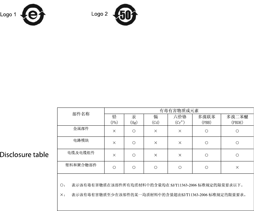
CMM labeling and disclosure table
CMM labeling and disclosure table■■■■■■■■■■■■■■■■■■■■■■■■■■■■■■■■■■■■■■■■■■■■■■■■■■■■■■■■■■■■■■
■
■
The P eople’s Republic of China require that our products comply with China Management
Methods (CMM) environmental regulations. (China Management Methods refers to the
regulation
Management Methods for Controlling P ollution by Electronic Information Products
).
T wo items are used to demonstrate compliance; the label and the disclosure table.
The label is placed in a customer visible position on the product.
•Logo 1 means the product contains no substances in excess of the maximum concentration
value for materials identified in the China Management Methods regulation.
•Logo 2 means that the product may contain substances in excess of the maximum
concentration value for materials identified in the China Management Methods regulation,
and has an Environmental Friendly Use P eriod (EFUP) in years, fifty years in the example
shown.
Logo 1 Logo 2
The Environmental Friendly Use P eriod (EFUP) is the period (in years) during which the T oxic
and Hazardous Substances (T&HS) contained in the Electronic Information Product (EIP)
will not leak or mutate causing environmental pollution, or bodily injury from the use of the
EIP . The EFUP indicated by the Logo 2 label applies to a product and all its parts. Certain
field -replaceable parts, such as battery modules, can have a different EFUP and are marked
separately .
The Disclosure table is intended only to communicate compliance with China requirements.
It is not intended to communicate compliance with EU RoHS or any other environmental
requirements.
10 68P09283A64 -3
FOA SEP 2007
Motorola document set
Motorola document set■■■■■■■■■■■■■■■■■■■■■■■■■■■■■■■■■■■■■■■■■■■■■■■■■■■■■■■■■■■■■■
■
■
The Motorola document sets provide the information to operate, install, and maintain the
Motorola equipment.
Ordering documents and CD -ROMs
W ith internet access available, to view , download, or order documents (original or revised), visit
the Motorola Lifecycles Customer web page at https://mynetworksupport.motorola.com , or
contact your Motorola account representative.
W ithout internet access available, order hard copy documents or CD -ROMs with your Motorola
Local Office or Representative.
If Motorola changes the content of a document after the original printing date, Motorola
publishes a new version with the same part number but a different revision character .
Document banner denitions
A banner (oversized text on the bottom of the page, for example, PRELIMINARY — UNDER
DEVELOPMENT ) indicates that some information contained in the document is not yet approved
for general customer use.
Data encryption
In order to avoid electronic eavesdropping, data passing between certain elements in the
network is encrypted. In order to comply with the export and import requirements of particular
countries, this encryption occurs at different levels as individually standardized, or may not be
present at all in some parts of the network in which it is normally implemented. The document
set, of which this document is a part, covers encryption as if fully implemented. Because the
rules differ in individual countries, limitations on the encryption included in the particular
software being delivered, are covered in the Release Notes that accompany the individual
software release.
68P09283A64 -3 11
SEP 2007 FOA

Third P art y Computer Softw are and T r ademarks
Third Party Computer Software and Trademarks■■■■■■■■■■■■■■■■■■■■■■■■■■■■■■■■■■■■■■■■■■■■■■■■■■■■■■■■■■■■■■
■
■
Computer Software
The Motorola and 3rd P arty supplied Software (SW) products described in this instruction
manual may include copyrighted Motorola and other 3rd P arty supplied computer programs
stored in semiconductor memories or other media. Laws in the United States and other
countries preserve for Motorola and other 3rd P arty supplied SW certain exclusive rights for
copyrighted computer programs, including the exclusive right to copy or reproduce in any
form the copyrighted computer program. Accordingly , any copyrighted Motorola or other
3rd P arty supplied SW computer programs contained in the Motorola products described in
this instruction manual may not be copied (reverse engineered) or reproduced in any manner
without the express written permission of Motorola or the 3rd P arty SW supplier . Furthermore,
the purchase of Motorola products shall not be deemed to grant either directly or by implication,
estoppel, or otherwise, any license under the copyrights, patents or patent applications of
Motorola or other 3rd P arty supplied SW , except for the normal non -exclusive, royalty free
license to use that arises by operation of law in the sale of a product.
V endor Copyright
Apache Software F oundation Copyright 2002-2003 All Rights Reserved
Artesyn
Copyright 2002-2003 All Rights Reserved
CMU *
Copyright 2002-2003 All Rights Reserved
Freeware T ools / Utilities * Copyright 2002-2003 All Rights Reserved
P erformance T echnologies Copyright 2002-2003 All Rights Reserved
T elelogic Copyright 2002-2003 All Rights Reserved
QNX *
Copyright 2002-2003 All Rights Reserved
*= Freeware
Trademarks
Java™ T echnology and/or J2ME™ : Java and all other Java -based marks are trademarks or
registered trademarks of Sun Microsystems, Inc. in the U .S . and other countries.
UNIX® : UNIX is a registered trademark of The Open Group in the United States and other
countries.
12 68P09283A64 -3
FOA SEP 2007

FCC R equirements
FCC Requirements
■■■■■■■■■■■■■■■■■■■■■■■■■■■■■■■■■■■■■■■■■■■■■■■■■■■■■■■■■■■■■■
■
■
Content
This section presents F ederal Communication Commissions (FCC) Rules P art 15 requirements
and compliance information for the USB CDMA XMI Transceiver at 1.9 GHz.
FCC Part 15 Requirements
Part 15.19a(3) - Information to User
This device complies with P art 15 of the FCC Rules. Operation is subject to the
following two conditions:
1. This device may not cause harmful interference, and
2. This device must accept any interference received, including interference that
may cause undesired operation
Part 15.21 - Information to User
Changes or modifications that change the FCC type approved configuration of the
equipment could void the user’s authority to operate the equipment.
68P09283A64 -3 13
SEP 2007 FOA

FCC R equirements
15.105(b) - Information to User
This equipment has been tested and found to comply with the limits for a Class B
digital device, under P art 15 of the FCC Rules. These limits are designed to provide
reasonable protection against harmful interference in a residential installation.
This equipment generates, uses and can radiate radio frequency energy and, if
not installed and used in accordance with the instructions, may cause harmful
interference to radio communications. However , there is no guarantee that
interference will not occur in a particular installation. If this equipment does cause
harmful interference to radio or television reception, which can be determined by
turning the equipment OFF and ON , the user is encouraged to try to correct the
interference by one or more of the following measures:
•Reorient or relocate the receiving antenna
•Increase the separation between the equipment and receiver .
•Connect the equipment into an outlet on a circuit different from that to which
the receiver is connected.
•Consult the dealer or an experienced radio/TV technician for help.
14 68P09283A64 -3
FOA SEP 2007

C h a p t e r
1
Overview
■■■■■■■■■■■■■■■■■■■■■■■■■■■■■■■■■■■■■■■■■■■■■■■■■■■■■■■■■■■■■■
■
■
■
■
68P09283A64 -3 1 -1
SEP 2007 FOA

Information Ov erview Chapter 1: Ov erview
Information Overview■■■■■■■■■■■■■■■■■■■■■■■■■■■■■■■■■■■■■■■■■■■■■■■■■■■■■■■■■■■■■■
■
■
•Before replacing components that are not covered in this manual, contact
Motorola Customer Network Resolution Center for special instructions that
may be involved.
•Many figures in this manual show typical equipment. The actual equipment
appearance may vary slightly .
Organization of manual
This manual is divided into the following main parts:
1 -2 68P09283A64 -3
FOA SEP 2007

1X UBS Macro B T S FRU Information Ov erview
•Chapter 1: Overview , covers:
Information Overview
UBS Macro BTS FRU Replacement Preview
UBS Macro BTS Product Overview
UBS Macro BTS Equipment Identification
External GPS (E -GPS) Module Equipment Identification
Integrated Duplexer RX Filter (IDRF) Equipment Identification
Site Span I/O (S SI) Module Equipment Identification
Transceiver Module Internal (XMI) Equipment Identification
Digital Module Internal (DMI) Equipment Identification
P ower Distribution Unit (PDU) Equipment Identification
RX Splitter Equipment Identification
P ower Supply Module (PSM) Shelf Equipment Identification
Optional RGPS Head Equipment Identification
•Chapter 2: Reference Procedures P erformed at BTS Site, covers:
Frame P ower Down & P ower -Up Procedures
•Chapter 3: Reference Procedures P erformed at OMCR, covers:
Accessing OMCR CLI W indow
Shut Down Site Signaling Functions for a P acket BTS
Restore Site Signaling Operations for a P acket BTS
•Chapters 4 through 12 covers:
Motorola Universal Base Station (UBS) Macro BTS FRU Procedures (see next
paragraph section)
BTS FRU procedures
The BTS FRU procedures are grouped by major functional areas within the Motorola Universal
Base Station (UBS) Macro BTS equipment and presented in the following individual chapters:
•Chapter 4: E -GPS Replacement Procedure
•Chapter 5: IDRF Replacement Procedure
68P09283A64 -3 1 -3
FOA SEP 2007

Information Ov erview Chapter 1: Ov erview
•Chapter 6: S SI Replacement Procedures
S SI (Site Span I/O) Module
Unbalanced E1 Daughter Card
QHSO (Quartz High Stability Oscillator)
•Chapter 7: XMI Replacement Procedures
XMI (Transceiver Module Internal) Module
XMI F an Tray Assembly
•Chapter 8: DMI Replacement Procedures
DMI (Digital Module Internal) Assembly
Modem Boards
•Chapter 9: PDU Replacement Procedures
P ower Distribution Unit (PDU)
Breaker Module Assembly (BMA)
•Chapter 10: PSM Shelf Replacement Procedures
–48 V DC P ower Supply Module (PSM) Shelf
220 V AC P ower Supply Module (PSM) Shelf
P ower Supply Modules (PSMs)
•Chapter 11: RX Splitter Replacement Procedure
•Chapter 12: RGPS Head Replacement Procedure
Each BTS FRU procedure section contains the following information:
•Description - contains general information about the FRU operation, usage and location in
the frame/shelf and so on.
•System impact/considerations - describes how the replacement procedure impacts the
system with respect to downtime and so on. It lists specific concerns associated with the
replacement of the FRU .
•Required items - lists items that are required to perform the FRU procedure including
reference documents (manuals), tools, torque requirements, and replacement unit.
•Prerequisite - highlights actions needed before and after the FRU replacement including:
coordinating the replacement procedure with the OMCR operator and so on.
•Replacement procedure - provides detailed procedural steps to remove the failed FRU
and install the replacement FRU including: site preparation, equipment disassembly and
reassembly , equipment and site operation restoration and so on. When necessary , the
procedural steps reference specific procedures to be performed by the OMCR operator .
1 -4 68P09283A64 -3
FOA SEP 2007
1X UBS Macro B T S FRU Information Ov erview
How to use this manual
All FRU replacement procedures require interaction and two -way communications between the
technician at the BTS site and the operator at the OMCR. Each of these individuals will need a
copy of this manual.
First determine the FRU to be replaced.
Next, the BTS technician at the site starts performing the replacement procedure for the
specific FRU . This procedure will direct the technician when to notify the operator at the OMCR
as to what action(s) to take. Often the OMCR operator action is to perform a specific procedure
contained in the FRU procedure chapter . When necessary , the specific FRU procedure will
direct the operator to notify the BTS technician that certain events have been completed and
what action(s) to take.
Depending on the specific FRU being replaced, the replacement procedure will be terminated by
either the BTS technician or the OMCR operator . Usually it is terminated by the OMCR operator
clearing old alarms and verifying that there are no new related alarms.
Required manuals
The following manuals are referenced in this manual and may be used for additional information
regarding replacement procedures.
•
1X UBS Macro BTS Hardware Installation
(68P09283A62) manual.
•
1X UBS Macro BTS Optimization/A TP
(68P09283A63) manual.
•
System Commands Reference
(68P09282A57) manual.
FRU locations
T o aid in physically identifying FRUs and locating the major functional areas of the equipment as
well as a specific FRU location, refer to the illustrations in the following sections of this chapter:
•UBS Macro BTS Equipment Identification
•External GPS (E -GPS) Equipment Identification
•Integrated Duplexer RX Filter (IDRF) Equipment Identification
•Site Span I/O (S SI) Module Equipment Identification
•Transceiver Module Internal (XMI) Equipment Identification
•Digital Module Internal (DMI) Equipment Identification
•P ower Distribution Unit (PDU) Equipment Identification
•RX Splitter Equipment Identification
•P ower Supply Module (PSM) Shelf Equipment Identification
•Optional RGPS Head Equipment Identification
68P09283A64 -3 1 -5
FOA SEP 2007

Information Ov erview Chapter 1: Ov erview
Recommended tools
Each BTS FRU procedure specifies the recommended tools that are required during the
procedure. These tools along with some other useful tools are included in the following overall
tool list:
•T orque driver , capable of 2.3 N -m (20 in -lbs) to 5.6 N -m (50 in -lbs) torque
•T25 TORX bit with 12 -in Extension
•T20 TORX bit
•T10 TORX bit
•19 mm open -end wrench (for N -type connectors)
•Flat blade screwdriver
•Side cutters
•Tie wraps
•Masking tape and marking pen (for making temporary cable markers)
•Removable XMI handle with two M5 screws
•SMA break over wrench - 1.02 N -M (9 in -lb)
•3/8 inch ratchet
•3/8 inch drive to 1/4 inch hex adapter
•19 mm socket
•10 mm socket
•9/16 in socket
Abbreviations and Acronyms
T able 1 -1 identifies the equipment related abbreviations and acronyms used in this manual.
Table 1 -1 Abbreviations and Acron yms
Acronym
Denition
1X
One of two bandwidths currently defined in the IS -2000 CDMA
specification, which extends the capability of the IS -95A and B
specifications. 1X bandwidth provides wireless packet voice and data
transmission capability at up to 144 Kbps.
A Ampere or Amp
AC
Alternating Current
ACC
Accessory
Continued
1 -6 68P09283A64 -3
FOA SEP 2007

1X UBS Macro B T S FRU Information Ov erview
Table 1 -1 Abbreviations and Acron yms (Continued)
Acronym
Denition
AN
Aggregation Node
A TP
Acceptance T est Plan
A WG American W ire Gauge
BMA
Breaker Module Assembly
BSI
Baseband Switch Interface
BS S Base Station System
BS SAN
Base Station System (BS S) Access Network. The BS SAN consists of a
R adio Access Network (RAN) and an AN . It may also include a Digital
Access and Cross-connect System to support split backhaul and a Selector
Distribution Unit (SDU).
BTS
Base Transceiver Station or Base Transceiver Subsystem
CB
Circuit Breaker
CBSC
Centralized Base Station Controller
CCW
Counter Clockwise
CDMA
Code Division Multiple Access
CE
Channel Element
CW
Clockwise
DC Direct Current
DIV
Diversity
DMI
Digital Module Internal
DMM
Digital Multi-Meter
E -GPS
External-GPS
ESD
Electro-Static Discharge
EV -DO
CDMA 1X Evolution - Data Only
FER Frame Erasure R ate
FRU
Field Replaceable Unit
FWD
F orward
GND
Ground
GPS
Global P ositioning System
HSO
High Stability Oscillator
IDI
Interworking DMI Interconnect
IDRF
Integrated Duplexer RX Filter
I/O Input/Output
IP
Internet Protocol
IP/OP
Customer Alarm Input/Output
Continued
68P09283A64 -3 1 -7
FOA SEP 2007

Information Ov erview Chapter 1: Ov erview
Table 1 -1 Abbreviations and Acron yms (Continued)
Acronym
Denition
IS
Interim Standard
LAN
Local Area Network
LMF
Local Maintenance F acility
LMT
Local Maintenance T erminal
MGB
Master Ground Bar
MMI
Man Machine Interface
MMII
Mobility Manager II
MSC
Mobile Switching Center
MSN
Mobile Switching Network
MSO
Motorola Standard Oscillator or Medium Stability Oscillator
OMC-IP
Operations Maintenance Center - Internet Protocol
OMC-R
Operations Maintenance Center - R adio
P A
P ower Amplifier
PBH
P acket Backhaul: IP -based backhaul between the BTS and the network.
The UBS Macro BTS is configured for packet backhaul operation.
PC P ower Connector
PDU
P ower Distribution Unit
PPS or 1PPS
1 pulse per second
PSM
P ower Supply Module
PSTN
Public Switched T elephone Network
QHSO
Quartz High Stability Oscillator
RAN
R adio Access Network
RF
R adio Frequency
RFL
Reflected
RGD
Remote GPS Distribution
RGPS
Remote Global P ositioning System
RS SI
Receive Signal Strength Indicator
RU
R ack Unit
RX
Receive or Receiver
SDU
Selection and Distribution Unit
SPROC Site Processor
S SI
Site Span I/O or Site/Span Interface
TCH
Traffic Channel
TX
Transmit or Transmitter
Continued
1 -8 68P09283A64 -3
FOA SEP 2007

1X UBS Macro B T S FRU Information Ov erview
Table 1 -1 Abbreviations and Acron yms (Continued)
Acronym
Denition
UBS
Motorola Universal Base Station
UNO
Universal Network Operations
V
V olt
VP U
V ocoder Processing Unit
W W att
XMI
Transceiver Module Internal
68P09283A64 -3 1 -9
FOA SEP 2007
UBS Macro B T S FRU R eplacement Preview Chapter 1: Ov erview
UBS Macro BTS FRU Replacement Preview■■■■■■■■■■■■■■■■■■■■■■■■■■■■■■■■■■■■■■■■■■■■■■■■■■■■■■■■■■■■■■
■
■
Passive and DC operation
Some FRUs are passive and do not have a DC input power source. Some FRUs are hot
swappable and can be removed/replaced with DC input power applied. Some FRUs require
shutdown of DC input power before FRU removal/replacement.
FRU backup
Some FRUs have a backup with fully -automatic switchover upon removal/replacement of the
primary .
Service affecting FRUs
FRUs that are service affecting require shutting down signaling to the entire BTS site before the
failed FRU can be removed/replaced.
Shutdown and restore signaling
The site shutdown and restore signaling procedure is performed by the OMC operator when
replacing certain FRUs.
Site shutdown signaling consists of the following sequence:
•Setup and turn ON Global Service Redirect Message to redirect all subscriber traffic
away from the site
•Disable or lock BTS
Site restore signaling consists of the following sequence:
•Enable or unlock BTS
•Reset and turn OFF Global Service Redirect Message
Testing/reoptimization
Some FRUs must be tested and if needed calibrated. Calibration requires that the BTS
site be shutdown/out -of -service or as an alternative In -Service Calibration procedure can be
used. The In -Service Calibration procedure does not require site outage. In some cases,
testing/reoptimization must be performed as part of the FRU replacement procedure. In other
cases, testing/reoptimization can be performed at the next maintenance window .
1 -10 68P09283A64 -3
FOA SEP 2007

1X UBS Macro B T S FRU UBS Macro B T S FRU R eplacement Preview
FRU replacement conditions and sequence
T able 1 -2 lists each FRU and the conditions and sequence of events required for replacement.
Table 1 -2 FRU replacement conditions and sequence
FRU Location Replacement conditions and sequence
E -GPS
(External-GPS)
UBS Macro frame The UBS Macro BTS will use one of the following backup
sources instead of the E -GPS:
•DMI controller board MSO which can maintain system
timing synchronization for up to 8 hours.
•Optional Quartz High Stability Oscillator (QHSO) which
can maintain system timing synchronization for up to
24 hours.
FRU is hot swappable .
•Replace FRU
IDRF
(Integrated
Duplexer RX
Filter)
UBS Macro frame FRU is passive; handles TX path, and RX path for both main
and diversity antennas for a particular sector .
1. Lock XMI
2. Replace IDRF
3. Unlock XMI
4. A t next maintenance window; TX P ath Calibration Audit
test affected sector TX path. RS SI test affected sector
RX paths
S SI (Site Span
I/O) Module
UBS Macro frame
1. Shut down signaling to Site and then DC input power
to S SI
2. Replace FRU
3. Apply DC input power to S SI
4. Restore signaling to Site
Unbalanced E1
Daughter Card
S SI front panel
FRU is passive.
1. Shut down signaling to Site
2. Replace FRU
3. Restore signaling to Site
QHSO (Quartz
High Stability
Oscillator)
S SI rear panel FRU is hot swappable and is a system timing
synchronization backup for the RGPS head.
1. Replace FRU
Continued
68P09283A64 -3 1 -11
FOA SEP 2007
UBS Macro B T S FRU R eplacement Preview Chapter 1: Ov erview
Table 1 -2 FRU replacement conditions and sequence (Continued)
FRU Location Replacement conditions and sequence
XMI
(Transceiver
Module
Internal)
Module
UBS Macro frame FRU is non-redundant.
1. Lock XMI
2. Shutdown DC input power to XMI
3. Replace XMI
4. Apply DC input power to XMI
5. Unlock XMI
6. Shut down signaling to Site (for calibration/audit) or
set up optional In-Service Calibration procedure
7. TX P ath Calibration Audit test all TX paths. RS SI test
all RX paths
8. Restore signaling to Site if In-Service Calibration
procedure was not used
XMI F an Tray
Assembly
UBS Macro frame, XMI
rear panel
See XMI Module above.
DMI (Digital
Module
Internal)
Assembly
UBS Macro frame
The DMI assembly is the FRU that can be used to
replace a DMI with an internal DMI component
failure (including controller board, modem board,
fan, or front panel failure).
1. Display BTS EID information to determine model
numbers of the failed DMI and its modem board(s).
2. F or a BTS with one DMI, Shut down signaling to Site .
F or a BTS with more than one DMI:
Status failed DMI to determine if Site Master or
not
If Site Master , Reset DMI and then Lock DMI
If not Site Master , Lock DMI
3. Shutdown DC input power to DMI
4. Replace DMI
5. Apply DC input power to DMI
Continued
1 -12 68P09283A64 -3
FOA SEP 2007

1X UBS Macro B T S FRU UBS Macro B T S FRU R eplacement Preview
Table 1 -2 FRU replacement conditions and sequence (Continued)
FRU Location Replacement conditions and sequence
6. F or a BTS with one DMI, Restore signaling to Site .
F or a BTS with more than one DMI, Unlock DMI
CDMA 1X
Modem Board
- OR -
CDMA EV -DO
Modem Board
Inside DMI FRU is non-redundant.
1. Display BTS EID information to determine model
numbers of the failed DMI and its modem board(s).
2. F or a BTS with one DMI, Shut down signaling to Site .
F or a BTS with more than one DMI:
Status affected DMI to determine if Site Master
or not
If Site Master , Reset DMI and then Lock DMI
If not Site Master , Lock DMI
3. Shutdown DC input power to DMI
4. Remove affected DMI assembly from UBS Macro BTS
frame
5. Replace Modem Board
6. Install affected DMI assembly into UBS Macro BTS
frame
7. Apply DC input power to DMI
8. F or a BTS with one DMI, Restore signaling to Site .
F or a BTS with more than one DMI, Unlock DMI
RX Splitter UBS Macro frame FRU is passive; handles EXP (expansion) RX main & diversity
antenna paths.
•Lock XMIs
•Replace FRU
•Unlock XMIs
•RS SI test affected RX paths at next maintenance
window; reoptimize as required
PDU (P ower
Distribution
Unit)
UBS Macro frame
1. Shut down signaling to Site and then power down the
frame
2. Replace FRU
3. P ower up the frame
4. Restore signaling to Site
Continued
68P09283A64 -3 1 -13
FOA SEP 2007

UBS Macro B T S FRU R eplacement Preview Chapter 1: Ov erview
Table 1 -2 FRU replacement conditions and sequence (Continued)
FRU Location Replacement conditions and sequence
Breaker Module
Assembly (BMA)
UBS Macro frame inside
of PDU
1. Shut down signaling to Site and then power down the
frame
2. Replace FRU
3. P ower up the frame
4. Restore signaling to Site
–48 V DC PSM
(P ower Supply
Module) Shelf
UBS Macro frame
1. Shut down signaling to Site and then power down the
frame
2. Replace FRU
3. P ower up the frame
4. Restore signaling to Site
220 V AC PSM
(P ower Supply
Module) Shelf
UBS Macro frame
1. Shut down signaling to Site and then power down the
frame
2. Replace FRU
3. P ower up the frame
4. Restore signaling to Site
–48 V DC or
220 V AC PSM
(P ower Supply
Module)
PSM shelf FRU is hot swappable and redundant .
1. Replace FRU
Optional RGPS
(Remote GPS)
Head
P ole/mast mounted
outdoors
The UBS Macro frame BTS uses one of the following backup
sources instead of the RGPS head:
•Internal Motorola Standard Oscillator (MSO) which
can maintain system timing synchronization for up to
8 hours.
•Optional Quartz High Stability Oscillator (QHSO) which
can maintain system timing synchronization for up to
24 hours.
FRU is hot swappable .
1. Replace FRU
1 -14 68P09283A64 -3
FOA SEP 2007

1X UBS Macro B T S FRU UBS Macro B T S Product Ov erview
UBS Macro BTS Product Overview■■■■■■■■■■■■■■■■■■■■■■■■■■■■■■■■■■■■■■■■■■■■■■■■■■■■■■■■■■■■■■
■
■
The R20 Motorola Universal Base Station (UBS) Macro BTS supports single band
800 MHz or 1.9 GHz RF band, up to two XMIs, up to two DMIs and one S SI. UBS
Macro BTS frame configurations with up to four XMIs and up to five DMIs will be
available in the future.
Introduction
The Motorola Universal Base Station (UBS) Macro BTS conforms to the TIA/EIA/IS -97E and
CDMA2000 for the CDMA Base Station performance specifications. It is a packet BTS that
operates in the 800 MHz or 1.9 GHz RF band.
The packet BTS has a packet backhaul network interface that can handle voice and data.
A packet BTS is equipped with IP -packet routing functionality . The packet BTS connects to
the Access Network (AN) using span lines. This configuration provides the packet backhaul
between the packet BTS and the AN .
UBS Macro BTS Frame Overview
The Motorola Universal Base Station (UBS) Macro BTS along with other external equipment
forms a 1X BTS that is part of the Motorola R adio Access Network (RAN).
The UBS Macro BTS is the interface between the Access Node (AN) in the RAN and the
Subscriber Units (SUs) that are operating in the UBS Macro BTS RF coverage area.
Control and bearer traffic data, in IP -packets, is exchanged between the UBS Macro BTS and the
AN . This IP -packet backhaul interconnection is through T1/E1 span lines or high -speed Ethernet.
Control and bearer traffic data is exchanged between the UBS Macro BTS and the SUs. This
interconnection is by means of the CDMA2000 1X air interface.
The UBS Macro BTS air interface supports the following:
•Omni or 3–sector antenna configurations
•Single RF band operation only; 800 MHz or 1.9 GHz RF band
•Up to 120 W of total TX RF power output and up to 30 W TX RF power output per carrier in
omni; 20W per sector -carrier in 3 sector
•Dual path, Main and Diversity , RX antennas
The UBS Macro BTS equipment is mounted in a 19–inch rack to form the UBS Macro BTS frame.
68P09283A64 -3 1 -15
FOA SEP 2007

UBS Macro B T S Product Ov erview Chapter 1: Ov erview
UBS Macro BTS frames are configured for either +27 V DC operation, –48 V DC operation, or
220 V AC operation.
UBS Macro BTS frames are also configured for low , mid, or high capacity . Capacity is determined
by the quantity of sector carriers and traffic channels supported by the frame. The quantity of
sector carriers is a function of the quantity of XMIs. The quantity of traffic channels is a function
of the quantity of modems. Because the modems are inside the DMI, the quantity of DMIs is a
capacity factor . The capacity of a UBS Macro BTS frame is essentially based on the following:
•low capacity - one XMI and up to two DMIs
•mid capacity - two XMIs and two DMIs
•high capacity - more than two XMIs (four XMIs maximum) and more than two DMIs (five
DMIs maximum)
Currently , only low and mid capacity frames are available/supported.
High capacity UBS Macro BTS frames will be available in the future.
The currently available UBS Macro BTS frames are shown in Figure 1 -1 UBS Macro BTS
low -tier/low -capacity frame (1000 mm rack) on page 1 - 27 ,Figure 1 -2 Low capacity UBS Macro
BTS starter frame (1800 mm rack) on page 1 - 28 and Figure 1 -3 UBS Macro BTS mid -capacity
frame (1800 mm rack) on page 1 - 30 .
UBS Macro BTS Frame Standard Equipment
All UBS Macro BTS frames, regardless of capacity , are equipped with at least one of each
of the following:
•IDRF (Integrated Duplexer RX Filter)
•S SI (Site Span I/O) module
•XMI (Transceiver Module Internal) module
•DMI (Digital Module Internal) module
•PDU (P ower Distribution Unit)
The following sections briefly describe the UBS Macro BTS frame standard equipment.
1 -16 68P09283A64 -3
FOA SEP 2007
1X UBS Macro B T S FRU UBS Macro B T S Product Ov erview
IDRF (Integrated Duplexer RX Filter)
The IDRF is available in either the 800 MHz or 1.9 GHz RF band.
The IDRF includes:
•TX/RX bandpass filters
•Bi -directional TX and RX antenna path couplers.
The IDRF is a passive device requiring no DC input operating power .
The IDRF allows the sector TX and main RX RF carrier signals to share the same antenna. It
also allows connection for a sector diversity RX RF antenna. The bi -directional antenna couplers
provide forward and reflected signal port connections for antenna signal sampling and signal
injection. The coupled ports are typically used for connection to test equipment.
The UBS Macro BTS frame is typically equipped with one IDRF per sector . Figure 1 -1 UBS
Macro BTS low -tier/low -capacity frame (1000 mm rack) on page 1 - 27 ,Figure 1 -2 Low capacity
UBS Macro BTS starter frame (1800 mm rack) on page 1 - 28 and Figure 1 -3 UBS Macro BTS
mid -capacity frame (1800 mm rack) on page 1 - 30 show the location of the IDRFs within the
UBS Macro frame.
Figure 1 -5 800 MHz IDRF I/O Details on page 1 - 32 and Figure 1 -6 1.9 GHz IDRF I/O Details on
page 1 - 33 show the locations of IDRF RF I/O port connectors.
68P09283A64 -3 1 -17
FOA SEP 2007
UBS Macro B T S Product Ov erview Chapter 1: Ov erview
SSI (Site Span I/O) module
The S SI provides the interfaces between the UBS Macro BTS frame and the following external
interfaces:
•IP -backhaul spans
The S SI directly supports up to 8 spans of packet backhaul through either balanced T1 or
E1 span lines. S SI can also be equipped with an optional unbalanced E1 daughter card that
transforms the S SI balanced E1 span line connections to 75 -ohm coaxial cable connections.
•IP -backhaul via Ethernet/OTI (Open Transport Interface)
•E -GPS module or RGPS head connects to the S SI RGPS connector . This connector may
also be used for the Sync Sharing Input connection from the SYNC SHARING connector of
another UBS Macro BTS frame S SI.
•Sync Sharing Output is present at the S SI SYNC SHARING connector . This connector
may be used for connection to the RGPS connector of another UBS Macro BTS frame
S SI. Chaining the SYNC SHARING connector of one UBS Macro BTS frame to the RGPS
connector of another UBS Macro BTS frame and so on provides sharing the GPS sync
signal between BTSs.
•Customer inputs/outputs; up to 24 customer defined inputs and up to 8 customer defined
outputs
•LMT (Local Maintenance T erminal); like the LMF (Local Maintenance F acility)
The S SI provides interfaces for the following UBS Macro BTS frame equipment:
•S SI DC power input – connects to the (PDU) P ower Distribution Unit.
•S SI -to -DMI interface – connects the S SI to up to two DMIs.
•HSO interface (on rear of S SI) – connects to the optional QHSO module.
1 -18 68P09283A64 -3
FOA SEP 2007
1X UBS Macro B T S FRU UBS Macro B T S Product Ov erview
XMI (Transceiver Module Internal) module
The UBS Macro XMIs are available in either the 800 MHz or 1.9 GHz RF band. The XMI
requires +27 V DC input operating power .
The XMI provides both the baseband transceiver and linear power amplifier functionality for the
BTS . This functionality is integrated within a single module. The XMI supports either a three
sector antenna configuration or an Omni (single sector) antenna configuration.
The XMI receiver is capable of supporting four carriers in the three -sector configuration and
eight carriers in the Omni configuration. On the forward link side, XMI can support up to
eight carriers in the three -sector configuration.
The XMI supports P A trunking, which enables dynamic TX RF power sharing among all
sector -carriers. An advantage of P A trunking is that power can be distributed among
sector -carriers with different loads. The built -in redundancy of trunking is also an advantage. If
one of the XMIs internal power amplifiers fails, all sector -carriers served by that XMI can still
operate at reduced power on the remaining power amplifiers. The XMI will generate a system
alarm to alert the operator of the failure condition, but will stay in service.
The XMI provides main and diversity receivers for three sectors. The UBS Macro BTS frame
supports soft -fail redundancy at the receiver level. If either the main and diversity receive path
fails, the XMI continues to operate with one receive path, but at reduced performance instead of
taking the entire XMI out -of -service.
68P09283A64 -3 1 -19
FOA SEP 2007
UBS Macro B T S Product Ov erview Chapter 1: Ov erview
DMI (Digital Module Internal) module
The DMI contains two main components: a controller board and at least one modem board (i.e.,
1X CDMA or EV -DO). The controller board provides interfaces for up to two modem boards (i.e.,
1X CDMA, EV -DO , or a combination of both). A DMI can be upgraded with a second modem
board depending upon the configuration required at the BTS .
In the forward direction (BTS to Mobile), the DMI terminates the backhaul control and bearer
connections from the S SI, processes the bearer and control data then routes the baseband
data to the XMI for conversion/RF modulation and transmission over the air interface to the
subscriber .
In the reverse direction (Mobile to BTS), the XMI receives the subscriber transmission over
the air interface. The XMI demodulates the received RF signal and converts it to baseband
data. The received baseband data is routed to the DMI for processing and generation to the
associated control and bearer data for transmission to the network via the S SI.
External interfaces on the DMI include the following:
•+27 V DC (nominal) power input
•T wo S SI interfaces
•T wo XMI interfaces
The controller board provides all of the DMI external interfaces as well as interfaces for two
modem boards. The controller is made up of the following functions: Site Processor (SPROC),
Synchronization, Interworking (protocol termination), DMI baseband processing, XMI interfaces
and S SI interface.
The DMI controller board also contains an Oven Controlled Crystal Oscillator (OCX O) that
is synchronized to the BTS system timing established/sourced by the E -GPS or Remote GPS
(RGPS) head. The OCX O also provides the MSO function. In the event that the GPS system
timing signal (i.e., E -GPS or RGPS or sync -sharing) is lost, the DMI controller can select the
MSO as a backup synchronization source for maintaining BTS system timing for up to 8 hours
PDU (Power Distribution Unit)
The PDU is the central power distribution point for the UBS Macro BTS frame. It contains input
power feeds that connect to the +27 V DC power output of one of the following:
•Optional –48 V DC PSM (P ower Supply Module) shelf
•Optional 220 V AC PSM shelf
•Customer supplied external +27 V DC power source
The PDU houses circuit breakers/power connectors for +27 V DC power distribution to each of
the following UBS Macro BTS frame subsystems:
•XMIs
•DMIs
•S SIs
•Accessories
The PDU also contains bulk capacitance to stabilize the internal bus voltage to facilitate
subsystem hot -swap and absorb surge energy .
1 -20 68P09283A64 -3
FOA SEP 2007
1X UBS Macro B T S FRU UBS Macro B T S Product Ov erview
UBS Macro BTS Frame Optional Equipment
The UBS Macro BTS frame may be equipped with following optional equipment:
•E -GPS (External GPS) module
•–48 V DC PSM (P ower Supply Module) shelf with PSMs
•220 V AC PSM (P ower Supply Module) shelf with PSMs
•QHSO (Quartz High Stability Oscillator) module
•Unbalanced E1 daughter card
•Modem boards
The following sections briefly describe the UBS Macro BTS frame optional equipment.
E -GPS (External GPS) module
The optional E -GPS contains a GPS Receiver (GPSR) that requires connection to an external GPS
RF antenna signal. The E -GPS output timing signal is routed to the DMI controller via the S SI.
The E -GPS is the primary source for BTS system timing.
The optional Remote GPS (RGPS) head may be used instead of the E -GPS .
The E -GPS is considered to be local with respect to the UBS Macro BTS frame, while the RGPS
head is remotely located with respect to the UBS Macro BTS frame.
–48 V DC PSM (Power Supply Module) shelf with PSMs
The –48 V DC PSM shelf is optional. It is used to convert –48 V DC input power to +27V DC
output operating power for distribution to the UBS Macro BTS frame electronics.
The –48 V DC PSM shelf is located at the bottom of the UBS Macro BTS frame. Figure 1 -1 UBS
Macro BTS low -tier/low -capacity frame (1000 mm rack) on page 1 - 27 ,Figure 1 -2 Low capacity
UBS Macro BTS starter frame (1800 mm rack) on page 1 - 28 and Figure 1 -3 UBS Macro BTS
mid -capacity frame (1800 mm rack) on page 1 - 30 show the location of the –48 V DC PSM shelf
within the UBS Macro BTS frame.
The plug -in PSMs provide DC -DC conversion and +27V DC power output capabilities.
Up to three PSMs can be housed in the PSM shelf . A minimum of two PSMs are equipped for
redundancy . An empty PSM 3 slot is covered with a filler panel.
68P09283A64 -3 1 -21
FOA SEP 2007
UBS Macro B T S Product Ov erview Chapter 1: Ov erview
220 V AC PSM (Power Supply Module) shelf with PSMs
The 220 V AC PSM shelf is optional. It is used to convert 220 V AC input power to +27V DC
output operating power for distribution to the UBS Macro BTS frame electronics.
The 220 V AC PSM shelf is located at the bottom of the UBS Macro BTS frame. Figure 1 -1 UBS
Macro BTS low -tier/low -capacity frame (1000 mm rack) on page 1 - 27 ,Figure 1 -2 Low capacity
UBS Macro BTS starter frame (1800 mm rack) on page 1 - 28 and Figure 1 -3 UBS Macro BTS
mid -capacity frame (1800 mm rack) on page 1 - 30 show the location of the 220 V AC PSM shelf
within the UBS Macro BTS frame.
The plug -in PSMs provide AC -DC conversion and +27V DC power output capabilities.
Up to three PSMs can be housed in the PSM shelf . A minimum of two PSMs are equipped for
redundancy . An empty PSM 3 slot is covered with a filler panel.
QHSO (Quartz High Stability Oscillator) module
The QHSO is an upgraded backup synchronization source for maintaining BTS system timing
established/sourced by the E -GPS or Remote GPS (RGPS) head. QHSO backup is used instead of
the internal DMI controller MSO . The QHSO can maintain BTS system timing for up to 24 hours,
as compared to 8 hours provided by the MSO .
The QHSO contains a high stability quartz crystal oscillator .
The optional QHSO is mounted on the S SI rear panel. It plugs directly into the S SI rear panel
HSO connector .
Unbalanced E1 daughter card
The optional E1 daughter card is located on the front panel of the S SI.
F or E1 daughter card location and connector identification, refer to Figure 1 -7 S SI front panel
details on page 1 - 35 .
The E1 daughter card has a 37 -pin connector on the bottom of the card. This connector plugs
into the SP AN 37 -pin connector on the front panel of the S SI.
The E1 daughter card is secured to the S SI front panel via four corner screws.
The E1 daughter card is passive and does not require DC operating power . The circuitry on
the E1 daughter card transforms 75–Ohm unbalanced span line I/O to 100–Ohm balanced
S SI span line I/O .
The E1 daughter card supports up to eight span lines. It has 16 BNC connectors, 2 per span;
RX and TX.
1 -22 68P09283A64 -3
FOA SEP 2007

1X UBS Macro B T S FRU UBS Macro B T S Product Ov erview
Modem boards
The modem board provides digital modulation/demodulation of the overhead channels and
traffic channels that are carried on the TX/RX RF carriers. The UBS Macro modem boards
are high density and have at least 256 channel elements that can be allocated to support the
desired quantity of overhead and traffic channels.
There are two types of UBS Macro modem boards available. These are as follows:
•1X CDMA modem board
•EV -DO modem board
The modem boards are located inside the DMI. A DMI can be equipped with up to two modem
boards maximum. These modem boards can be either 1X CDMA modem, EV -DO modem, or
one of each.
UBS Macro BTS Frame Optional External Equipment
The RGPS (Remote GPS) head is optional external equipment for the UBS Macro BTS frame.
The following section briefly describes the RGPS head.
RGPS (Remote GPS) head
The optional RGPS head contains a GPS antenna GPS Receiver (GPSR) and built -in GPS RF
antenna. The RGPS head output timing signal is routed to the DMI controller via the S SI.
The RGPS head is the primary source for BTS system timing.
UBS Macro BTS FRU List
Before replacing components that are not covered in this manual, contact Motorola
Customer Network Resolution Center for special instructions that may be involved.
Each BTS FRU procedure specifies the required FRU(s) along with its model/part number .
T able 1 -3 lists all the supported UBS Macro BTS FRUs.
68P09283A64 -3 1 -23
FOA SEP 2007

UBS Macro B T S Product Ov erview Chapter 1: Ov erview
Table 1 -3 UBS Macro B T S FRUs
FRU item Motorola Model/P art number
(unless specified otherwise)
E -GPS ST TG4052
IDRF , China Full Band 800 MHz
STFN4009
IDRF , India Full Band 800 MHz
STFN4010
IDRF , US Full Band 800 MHz
STFN4015
IDRF , US A-band 800 MHz
STFN4016
IDRF , US B -band 800 MHz
STFN4017
IDRF , 1.9 GHz STFG4055
S SI STLN6390
Unbalanced E1 Daughter Card
STLN6327
QHSO SGLA4017
XMI, 800 MHz; with removable handle attached
SGTF4194
XMI, 1.9 GHz; with removable handle attached
STWG4000
XMI F an Tray Assembly; with five 27 V DC fans
STLN6404
All models of DMI assemblies include: DMI chassis with controller board, fans
and front panel.
DMI assembly with one 1X CDMA modem board
STLN6681
DMI assembly with one EV -DO modem board
STLN6682
DMI assembly with two 1X CDMA modem boards
STLN6683
DMI assembly with one 1X CDMA modem board and
one EV -DO modem board
STLN6684
DMI assembly with two EV -DO modem boards
STLN6679
DMI assembly without modem boards
STLN6325
CDMA 1X Modem Board
SGLN6336
EV -DO Modem Board
SGLN6494
RX Splitter , wide band (800 MHz through 2.1 GHz
RF bands)
STRG4029
PDU
STPN4038
90A BMA for XMIs
STLN4093
20A BMA for DMIs and S SIs
STLN6472
Continued
1 -24 68P09283A64 -3
FOA SEP 2007

1X UBS Macro B T S FRU UBS Macro B T S Product Ov erview
Table 1 -3 UBS Macro B T S FRUs (Continued)
FRU item Motorola Model/P art number
(unless specified otherwise)
10A BMA for ACCs
STLN6475
–48 V DC PSM Shelf; without PSMs
STHN4089
220 V AC PSM Shelf; without PSMs
STHN4092
–48 V DC PSM STPN4037
220 V AC PSM STPN4036
Optional RGPS Head
STLN6594
68P09283A64 -3 1 -25
FOA SEP 2007
UBS Macro B T S Equipment Identication Chapter 1: Ov erview
UBS Macro BTS Equipment Identication■■■■■■■■■■■■■■■■■■■■■■■■■■■■■■■■■■■■■■■■■■■■■■■■■■■■■■■■■■■■■■
■
■
Low and mid capacity UBS Macro BTS Frames
All Motorola Universal Base Station (UBS) Macro BTS frames are configured for either 800
MHz or 1.9 GHz RF band operation.
F or software release 2.20.0.x, only low and mid capacity UBS Macro BTS frames are available.
There are two versions low capacity UBS Macro BTS frames:
•UBS Macro BTS frame/short rack (see Figure 1 -1 )
•UBS Macro BTS starter frame/tall rack (see Figure 1 -2 )
The starter frame/tall rack can be easily expanded with equipment in the future to become a
mid or high capacity frame.
The frame/short rack cannot be easily expanded. Equipment expansion of this frame/short
rack would require equipment disassembly and then reassembly similar to that of the starter
frame in a taller rack. Typically the frame/short rack equipment configuration is used because
there is no plan for frame expansion.
1 -26 68P09283A64 -3
FOA SEP 2007
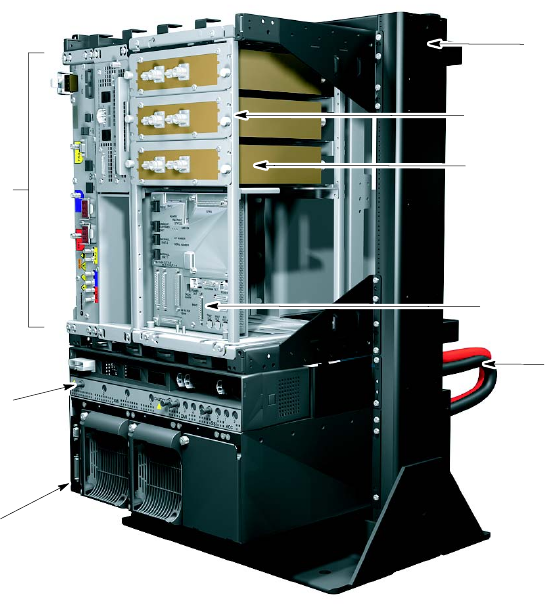
1X UBS Macro B T S FRU UBS Macro B T S Equipment Identication
Figure 1 -1 UBS Macro B T S low -tier/low -capacit y fr ame (1000 mm r ack)
ti-cdma-05993.eps
IDRF (Integrated Duplexer and
RX Filter) Shelf
SSI (Site Span I/O); SSI 1
XMI (Transceiver Module Internal) Shelf
- One XMI; XMI 1 (800 MHz or 1.9 GHz
See Notes 2, 3)
- Up to 2 DMIs (Digital Module Internal)
just right of XMI 1
- DMI 1, top; optional DMI 2 or empty
housing, bottom
- IDRF (Integrated Duplexer and RX Filter)
Shelf; in right side of XMI shelf
PDU (+27 V DC Power Distribution Unit)
- One: +27 V DC XMI Power Connector
(PC) and 90A Circuit Breaker (CB)
- Up to 2: +27 V DC DMI PCs and 20A CBs
- One: +27 V DC SSI PC and 20A CB
- No +27 V DC Accessory PCs and CBs
PSM (Power Supply Module) Shelf #1
(See Notes 4,5,6)
- Up to 2 PSMs
- Empty PSM slot with filler panel
- PSM 1 through 3 (left-to-right)
NOTES:
1. Interconnect cabling not shown for clarity.
2. 800 MHz equipment shown; 1.9 GHz similar.
3. 800 MHz XMI is 86 mm wide. 1.9 GHz XMI is 106.3 mm wide.
4. PSM shelf is optional and used instead of +27 V DC power Input.
5. PSM shelf is either -48 V DC or AC.
6. Only -48 V DC PSMs can be used in -48 V DC PSM shelf. Only AC PSMs can be used in AC PSM shelf.
PSM Shelf #1
+27 V DC Power
Cabling
Equipment
Mounting Rack
IDRF (800 MHz or 1.9 GHz
See Note 2)
- Up to 3 IDRFs; one per sector
- IDRF sector 1 through sector 3
(top-to-bottom)
- Antenna RF I/O, front
- BTS RF I/O, rear
68P09283A64 -3 1 -27
FOA SEP 2007
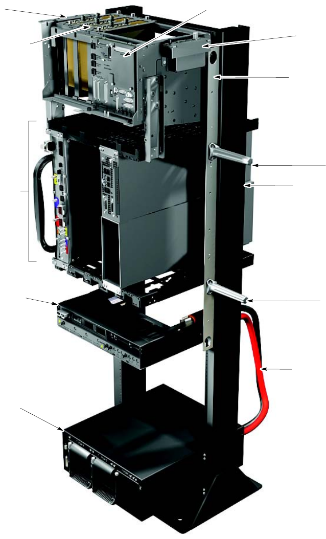
UBS Macro B T S Equipment Identication Chapter 1: Ov erview
Figure 1 -2 Low capacit y UBS Macro B T S starter fr ame (1800 mm r ack)
ti-cdma-05994.eps
IDRF (Integrated Duplexer and RX Filter) Shelf
- Up to 3 IDRFs (800 MHz or 1.9 GHz
See Note 2); one per sector
- IDRF sector 1 through sector 3 (left-to-right)
- Antenna RF I/O, top
- BTS RF I/O, bottom
SSI (Site Span I/O)
- One SSI; SSI 1
RX Antenna Sharing Bracket
E-GPS Module
XMI (Transceiver Module Internal) Shelf
- One XMI; XMI 1 (800 MHz or 1.9 GHz
See Notes 2, 3) XMI shelf slot 1
- Up to 2 DMIs (Digital Module Internal)
XMI shelf slot 4
- DMI 1, top; optional DMI 2 or empty
housing, bottom
PDU (+27 VDC Power Distribution Unit)
See Note 8
- One: +27 VDC XMI Power Connector
(PC) and 90A Circuit Breaker (CB)
- Up to 2: +27 VDC DMI PCs and 20A CBs
- One: +27 VDC SSI PC and 20A CB
- No +27 VDC Accessory PCs and CBs
PSM (Power Supply Module) Shelf #1
(See Notes 4,5,6)
- Up to 3 PSMs
- Empty PSM slot with filler panel
- PSM 1 through 3 (left-to-right)
NOTES:
1. Interconnect cabling not shown for clarity.
2. 800 MHz equipment shown; 1.9 GHz similar.
3. 800 MHz XMI is 86 mm wide. 1.9 GHz XMI is 106.3 mm wide.
4. PSM shelf is optional and used instead of+27 VDC power Input.
5. PSM shelf is either -48 VDC or AC.
6. Only -48 VDC PSMs can be used in -48 VDC PSM shelf. Only AC PSMS can be used in AC PSM shelf.
7. Carrier strips are removable.
8. PDU may be moved down 6 rack units to ease future expansion.
PSM Shelf #1
+27 VDC Power
Cabling
Handle
Equipment
Mounting Rack
Handle
Carrier Strip with
Removable Lifting
Handles (one strip
on each side of rack)
See Note 7
1 -28 68P09283A64 -3
FOA SEP 2007
1X UBS Macro B T S FRU UBS Macro B T S Equipment Identication
A typical mid capacity frame is shown in Figure 1 -3 .
The mid capacity frame is essentially a starter frame/tall rack that is already expanded to mid
capacity . The mid capacity frame can be expanded with equipment in the future to become a
high capacity frame.
68P09283A64 -3 1 -29
FOA SEP 2007
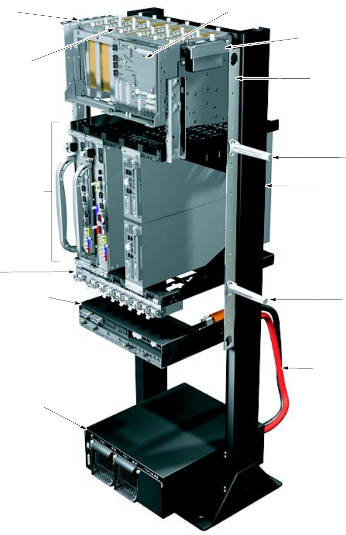
UBS Macro B T S Equipment Identication Chapter 1: Ov erview
Figure 1 -3 UBS Macro B T S mid -capacit y fr ame (1800 mm r ack)
ti-cdma-05995.eps
IDRF (Integrated Duplexer and RX Filter) Shelf
- Up to 6 IDRFs (800 MHz or 1.9 GHz
See Note 2); two sets of IDRFs,
each set with one IDRF per sector
- IDRF sector 1 through sector 3 (left-to-right)
- Antenna RF I/O, top
- BTS RF I/O, bottom
SSI (Site Span I/O)
- One SSI; SSI 1
XMI (Transceiver Module Internal) Shelf
- Two XMIs (800 MHz or 1.9 GHz
See Notes 2, 3); XMI 1, XMI 2 in
XMI shelf slots 1, 2
- Two DMIs (Digital Module Internal)
XMI shelf slot 4
- DMI 1, top; DMI 2, bottom
PDU (+27 VDC Power Distribution Unit)
See Note 8
- One: +27 VDC XMI Power Connector
(PC) and 90A Circuit Breaker (CB)
- Up to 2: +27 VDC DMI PCs and 20A CBs
- One: +27 VDC SSI PC and 20A CB
- No +27 VDC Accessory PCs and CBs
PSM (Power Supply Module) Shelf #1
(See Notes 4,5,6)
- Up to 3 PSMs
- Empty PSM slot with filler panel
- PSM 1 through 3 (left-to-right)
NOTES:
1. Interconnect cabling not shown for clarity.
2. 800 MHz equipment shown; 1.9 GHz similar.
3. 800 MHz XMI is 86 mm wide. 1.9 GHz XMI is 106.3 mm wide.
4. PSM shelf is optional and used instead of+27 VDC power Input.
5. PSM shelf is either -48 VDC or AC.
6. Only -48 VDC PSMs can be used in -48 VDC PSM shelf. Only AC PSMS can be used in AC PSM shelf.
7. Carrier strips are removable.
8. PDU may be moved down 6 rack units to ease future expansion.
PSM Shelf #1
+27 VDC Power
Cabling
Handle
Equipment
Mounting Rack
Handle
Carrier Strip with
Removable Lifting
Handles (one strip
on each side of rack)
See Note 7
RX Splitter
RX Antenna Sharing Bracket
E-GPS Module
1 -30 68P09283A64 -3
FOA SEP 2007
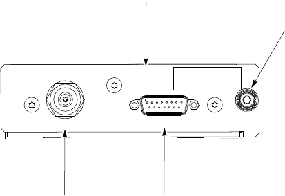
1X UBS Macro B T S FRU External GPS (E -GPS) Equipment Identication
External GPS (E -GPS) Equipment Identication■■■■■■■■■■■■■■■■■■■■■■■■■■■■■■■■■■■■■■■■■■■■■■■■■■■■■■■■■■■■■■
■
■
E -GPS I/O Details
The UBS Macro BTS frame is equipped with an E -GPS module. The E -GPS module contains a
GPS receiver (GPSR).
The E -GPS module connects to an external GPS RF antenna. It also connects to the S SI. The S SI
and its associated DMI cabling routes the E -GPS module GPSR output signals to the controller
board inside of the DMI. .
The E -GPS module operates from DC input power provided by the S SI connection.
See Figure 1 -4 for E -GPS module I/O connectors location and details.
Figure 1 -4 E -GPS I/O Details
ti-cdma-06499.eps
GPS-ANT SSI-GPS
Thumbscrew
E-GPS
Module
15-pin D-type
Connector to
RGPS Connector
on SSI
Coaxial Cable
Connector (N-type)
to External GPS
RF Antenna
68P09283A64 -3 1 -31
FOA SEP 2007
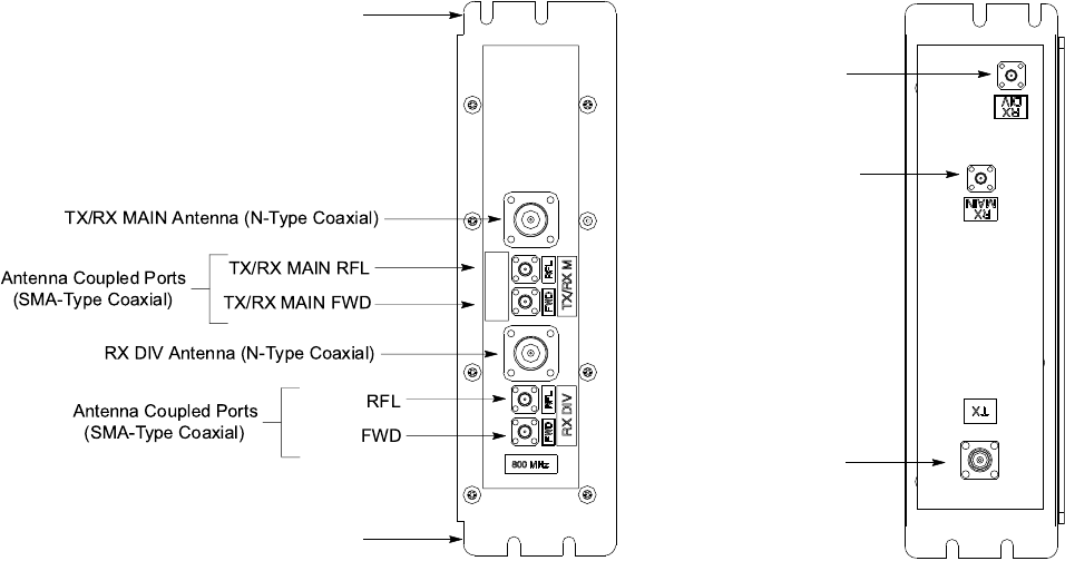
Integr ated Duplex er RX Filter (IDRF) Equipment Identication Chapter 1: Ov erview
Integrated Duplexer RX Filter (IDRF) Equipment
Identication
■■■■■■■■■■■■■■■■■■■■■■■■■■■■■■■■■■■■■■■■■■■■■■■■■■■■■■■■■■■■■■
■
■
IDRF I/O Details
The UBS Macro BTS antenna I/O equipment consists of the IDRF (Integrated Duplexer and RX
Filter) with dual directional couplers for each antenna port.
The UBS Macro BTS frame is equipped with one IDRF per sector antenna.
The IDRFs are passive devices and therefore do not require DC input power for operation.
The BTS Antennas connect to the front of the IDRF while the BTS frame equipment connects to
the rear of the IDRF .
RF test equipment can be connected to the directional couplers located on the front of the IDRF .
These ports allow RF signal monitoring of the antenna paths as well as RF signal injection into
the BTS equipment antenna paths.
See the applicable Figure 1 -5 or Figure 1 -6 for IDRF I/O connectors location and details.
Figure 1 -5 800 MHz IDRF I/O Details
TOP VIEW BOTTOM VIEW
RX DIV to XMI
(QMA-Type Coaxial)
TX from XMI
(Sector TX RF)
(QN-Type Coaxial)
RX MAIN to XMI
(QMA-Type Coaxial)
ti-cdma-06010.eps
TX/RX MAIN Antenna (N-T ype Coaxial)
Antenna Coupled Ports
(SMA-Type Coaxial)
TX/RX MAIN RFL
TX/RX MAIN FWD
Antenna Coupled Ports
(SMA-Type Coaxial)
RX DIV
RFL
RX DIV
FWD
RX DIV Antenna (N-T ype Coaxial)
(Sector RX RF)
(Sector RX RF)
TX/RX M
RX DIV
FWD CPLR
LABEL
Mounting Tab
Mounting Tab
NOTE:
1. Connector locations may vary
depending on the IDRF supplier.
1 -32 68P09283A64 -3
FOA SEP 2007
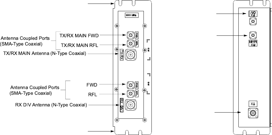
1X UBS Macro B T S FRU Integr ated Duplex er RX Filter (IDRF) Equipment Identication
Figure 1 -6 1.9 GHz IDRF I/O Details
TOP VIEW BOTTOM VIEW
RX DIV to XMI
(QMA-Type Coaxial)
TX from XMI
(Sector TX RF)
(QN-Type Coaxial)
RX MAIN to XMI
(QMA-Type Coaxial)
ti-cdma-06009.eps
TX/RX MAIN Antenna (N-T ype Coaxial)
Antenna Coupled Ports
(SMA-Type Coaxial)
RX DIV
RFL
RX DIV
FWD
Antenna Coupled Ports
(SMA-Type Coaxial) TX/RX MAIN RFL
TX/RX MAIN FWD
RX DIV Antenna (N-T ype Coaxial)
Mounting Tab
(Sector RX RF)
(Sector RX RF)
Mounting Tab
NOTE:
1. Connector locations may vary
depending on the IDRF supplier.
68P09283A64 -3 1 -33
FOA SEP 2007
Site Span I/O (S SI) Module Equipment Identication Chapter 1: Ov erview
Site Span I/O (SSI) Module Equipment Identication■■■■■■■■■■■■■■■■■■■■■■■■■■■■■■■■■■■■■■■■■■■■■■■■■■■■■■■■■■■■■■
■
■
SSI I/O Details
See Figure 1 -7 for S SI front panel I/O connectors location and details.
1 -34 68P09283A64 -3
FOA SEP 2007
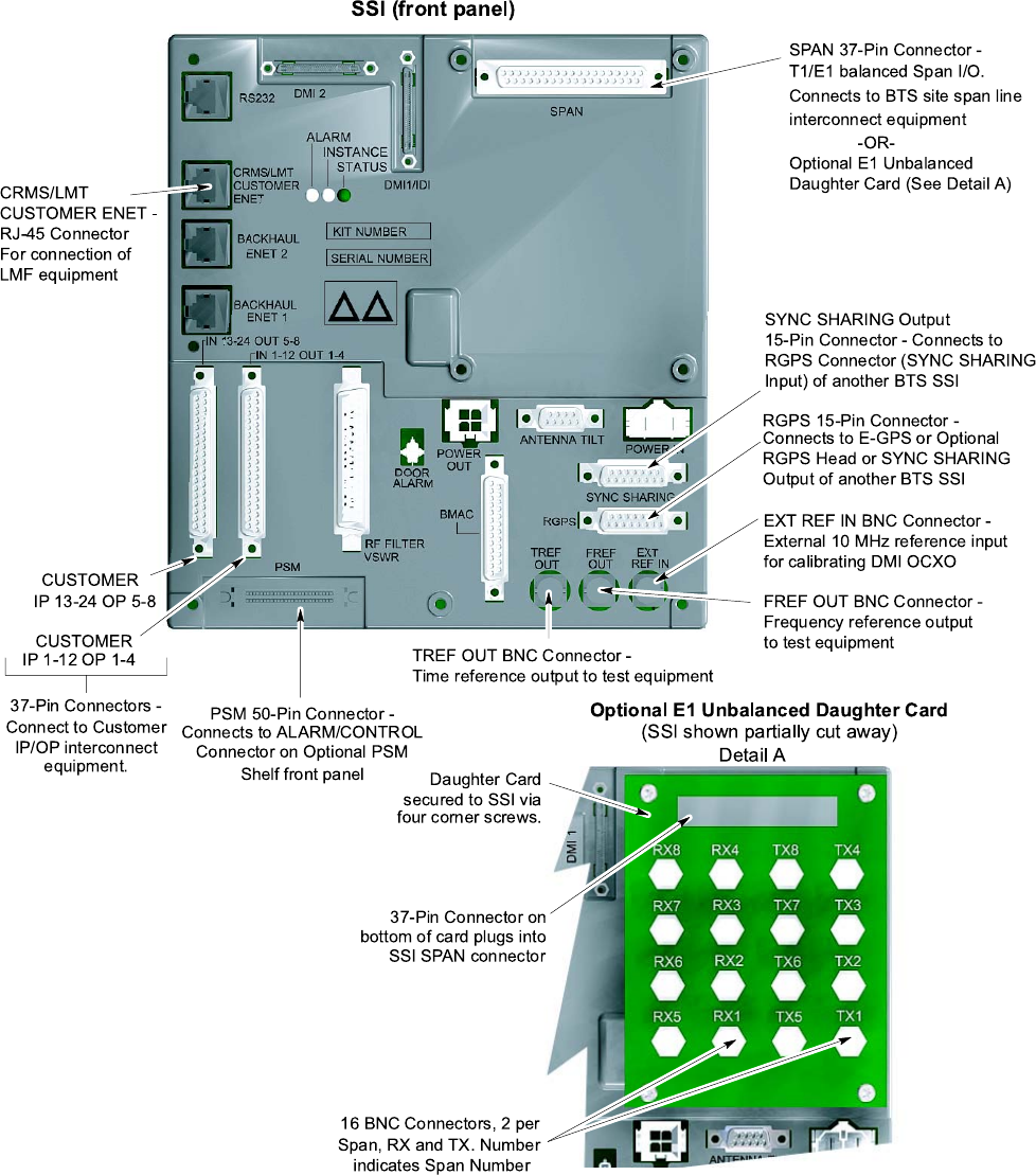
1X UBS Macro B T S FRU Site Span I/O (S SI) Module Equipment Identication
Figure 1 -7 S SI front panel details
SSI (front pane l)
CUST OMER
IP 13-24 OP 5-8
CUST OMER
IP 1-12 OP 1-4
37-Pin Connectors -
Connect to Customer
IP/OP interconnect
equipment.
PSM 50-Pin Connector -
Connects to ALARM/CONTROL
Connector on Optional PSM
Shelf front panel
RGPS 15-Pin Connector -
Connects to E-GPS or Optional
RGPS Head or SYNC SHARING
Output of another BTS SSI
SP AN 37-P in Connector -
T1/E1 balanced Span I/O.
Connects to BTS site span line
interconnect equipment
-OR-
Optional E1 Unbalanced
Daughter Card (See Detail A)
Detail A
Optional E1 Unbalanced Daughter Card
(SSI sh own partially cut away)
Dau ghter Card
sec ured to SSI via
four corner scre ws.
37-Pin C onnector on
bottom o f card plugs into
SSI SP AN connector
16 BNC Conn ectors , 2 per
Span , RX an d TX. Number
indicates S pan Number
ti-cdma-05698.eps
TREF OUT BNC Connector -
Time reference o utput to test equipment
FREF OUT BNC Connector -
Frequenc y refere nce output
to test equipmen t
EXT REF IN BNC Connector -
External 10 MH z reference input
for calibrating DM I OCXO
CRMS/LMT
CUST OMER EN ET -
RJ-45 Connector
For connection o f
LMF equipment
SYNC SHARING Output
15-Pin Connector - Connects to
RGPS Connector (SYNC SHARING
Input) of another BTS SSI
68P09283A64 -3 1 -35
FOA SEP 2007
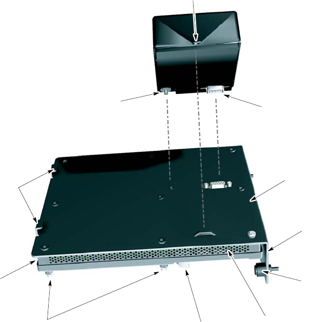
Site Span I/O (S SI) Module Equipment Identication Chapter 1: Ov erview
See Figure 1 -8 for S SI rear panel I/O connector location and details.
Figure 1 -8 S SI rear panel details
ti-cdma-05911.eps
QHSO
(Optional )
SSI (rear panel)
SSI Mounting Bracket
SPAN Connector End
Optional E1 Daughter
Card Mounting POWER IN
Connector
SSI
Module
Mounting Hooks
Captive Thumbscrew
(one of two; second on
other end of flange)
Right Anle
Mounting Flange
Captive Thumbscrew
Mounting Tab
9-pin Connector
1 -36 68P09283A64 -3
FOA SEP 2007
1X UBS Macro B T S FRU T r ansceiv er Module Internal (XMI) Equipment Identication
Transceiver Module Internal (XMI) Equipment
Identication
■■■■■■■■■■■■■■■■■■■■■■■■■■■■■■■■■■■■■■■■■■■■■■■■■■■■■■■■■■■■■■
■
■
XMI I/O Details
Figure 1 -9 shows I/O connectors on the front panel of the UBS Macro BTS 800 MHz XMI.
Figure 1 -10 shows I/O connectors on the front panel of the UBS Macro BTS 1.9 GHz XMI. The
top -to -bottom positioning of the XMI shown in the figures is the same as when it is installed in
the rack. These figures show connector/port locations, connector types and brief cabling details.
68P09283A64 -3 1 -37
FOA SEP 2007
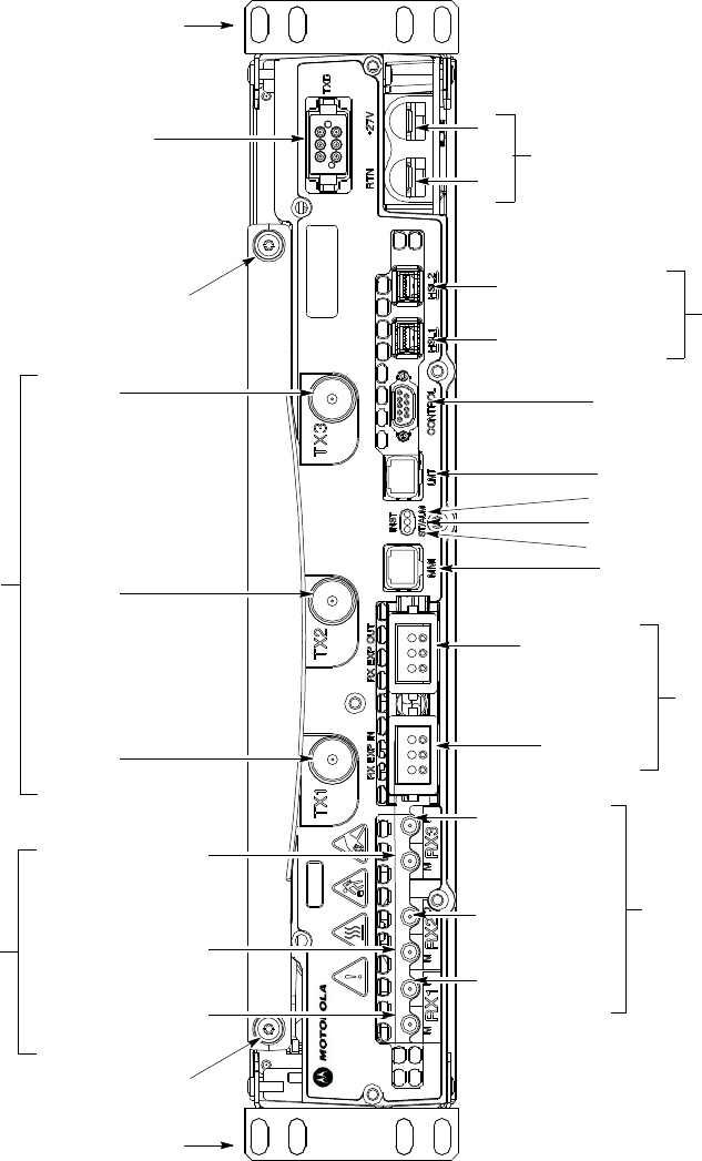
T r ansceiv er Module Internal (XMI) Equipment Identication Chapter 1: Ov erview
Figure 1 -9 800 MHz XMI Module Front P anel I/O Detail
800 MHz
ti-cdma-06385.eps
Mounting Tab
RX EXP IN
RX EXP OUT
TOP
MMI (RJ45) Note 2
(+)
(-)
+27V DC Input Power
From PDU
HSL2; to/from DMI-2
(HSSDC2 Type)
HSL1; to/from DMI-1
RX DIV
RX 1; from
Sector 1 IDRF
RX 2; from
Sector 2 IDRF
RX 3; from
Sector 3 IDRF
RX MAIN
RX 1; from Sector
1 IDRF
RX 2; from Sector
2 IDRF
RX 3; from Sector
3 IDRF
TX-3; to
Sector 3 IDRF
TX-2; to
Sector 2 IDRF
TX-1; to
Sector 1 IDRF
Handle Mounting
Screw Hole
TX RF Outputs
(QN-type coaxial)
Mounting Tab
BOTTOM
NOTES:
1. Equipment shown is typical. Actual equipment
appearance may vary slightly.
2. LMT and MMI ports are used by Motorola for testing
or debugging purposes. These ports may be used by
customers for maintenance purposes. Carefully follow
written procedures when using these ports in the field.
Failure to do so could result in an inoperable FRU.
Handle Mounting
Screw Hole
TXD (ganged MCX-type)
To/From TX Combiner; Future Use
(For proper XMI TX RF Outputs operation,
the TXD port must be terminated with
TXD Attenuator, Motorola part number
5888774T01, if XMI is not cabled to
TX Combiner)
(QMA-Type Coaxial)
Always used on XMI 1;
Never used on XMI 2
(QMA-Type Coaxial)
Always used on XMI 2;
Only used on XMI 1 if
XMI 2 is not equipped
RX Expansion Ports
(ganged mini-coaxial)
To/From RX Splitter or
RX Cross-Connect Cable
CONTROL( 9-pin D-type)
To/From TX Combiner; Future Use
ALM (Alarm) LED
STA (Status) LED
INST (Instance) LED
LMT (RJ45) Note 2
1 -38 68P09283A64 -3
FOA SEP 2007
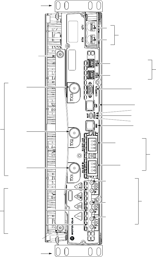
1X UBS Macro B T S FRU T r ansceiv er Module Internal (XMI) Equipment Identication
Figure 1 -10 1.9 GHz XMI Module Front P anel I/O Detail
1.9 GHz
ti-cdma-06109.eps
Mounting Tab
RX EXP IN
RX EXP OUT
TOP
MMI (RJ45) Note 2
CONTROL
LMT (RJ45) Note 2
(+)
(-)
+27V DC Input Power
From PDU
HSL2; to/from DMI-2
(HSSDC2 Type)
HSL1; to/from DMI-1
RX DIV
RX 1; from
Sector 1 IDRF
RX 2; from
Sector 2 IDRF
RX 3; from
Sector 3 IDRF
RX MAIN
RX 1; from Sector
1 IDRF
RX 2; from Sector
2 IDRF
RX 3; from Sector
3 IDRF
TX-3; to
Sector 3 IDRF
TX-2; to
Sector 2 IDRF
TX-1; to
Sector 1 IDRF
Handle Mounting
Screw Hole
Handle Mounting
Screw Hole
TX RF Outputs
(QN-type coaxial)
Mounting Tab
BOTTOM
ALM (Alarm) LED
STA (Status) LED
INST (Instance) LED
(QMA-Type Coaxial)
Always used on XMI 1;
Never used on XMI 2
(QMA-Type Coaxial)
Always used on XMI 2;
Only used on XMI 1 if
XMI 2 is not equipped
RX Expansion Ports
(ganged mini-coaxial)
To/From RX Splitter or
RX Cross-Connect Cable
Not Used
NOTES:
1. Equipment shown is typical. Actual equipment
appearance may vary slightly.
2. LMT and MMI ports are used by Motorola for testing
or debugging purposes. These ports may be used by
customers for maintenance purposes. Carefully follow
written procedures when using these ports in the field.
Failure to do so could result in an inoperable FRU.
68P09283A64 -3 1 -39
FOA SEP 2007
Digital Module Internal (DMI) Equipment Identication Chapter 1: Ov erview
Digital Module Internal (DMI) Equipment Identication■■■■■■■■■■■■■■■■■■■■■■■■■■■■■■■■■■■■■■■■■■■■■■■■■■■■■■■■■■■■■■
■
■
DMI I/O Panel
Figure 1 -11 shows I/O connectors on the front panel of the UBS Macro BTS DMI. The
top -to -bottom positioning of the DMI shown in the figure is the same as when it is installed in
the rack. This figure shows connector/port locations, connector types and brief cabling details.
1 -40 68P09283A64 -3
FOA SEP 2007
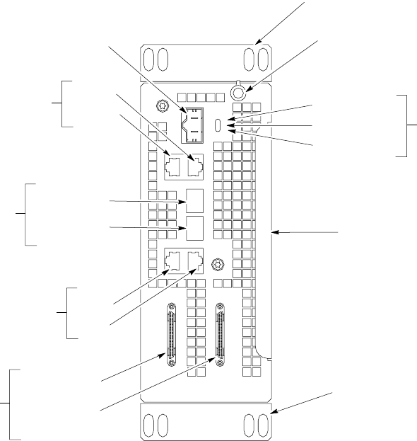
1X UBS Macro B T S FRU Digital Module Internal (DMI) Equipment Identication
Figure 1 -11 DMI Module Front P anel Detail
LMT
IDI/SSI1
SSI2
TEST XMI1/BSI XMI2 RS232-2
RS232-1
+27VDC
INST
ST ALM
ti-cdma-05912.eps
Mounting Tab
TOP Retaining Fastener
(Retains DMI Chassis
to DMI Cage)
MMI Serial Debug
Ports (RJ45)
Note 2
+27 V DC Input
Power From PDU
(mini-Molex)
Ethernet 10/100 BaseT
Debug Ports (RJ45)
Note 2
LMT
TEST
Serial Backhaul;
Traffic & Control Data
(VHDCI Typel)
To/From SSI-1
To/From SSI-2
(Future Use)
Mounting Tab
NOTES:
1. Equipment shown is typical. The actual equipment appearance may vary slightly.
2. The debug ports are intended to be used primarily for testing or debugging purposes by Motorola.
These ports may be used in the field for maintenance purposes by customers. Carefully follow written
procedures when using these ports in the field. Failure to do so could result in an inoperable FRU.
BOTTOM
Handle
To/From XMI-2
To/From XMI-1
LEDs
ST (Status)
ALM (Alarm)
INST (Instance)
1.2288 Gbps high-speed
serial data links (SFP Type).
Carries XMI baseband I & Q
data as well as control data
RS232-2
RS232-1
68P09283A64 -3 1 -41
FOA SEP 2007
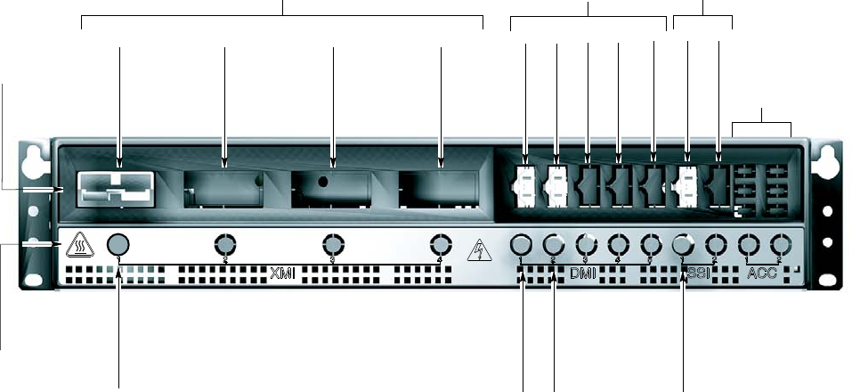
P ower Distribution Unit (PDU) Equipment Identication Chapter 1: Ov erview
Power Distribution Unit (PDU) Equipment Identication■■■■■■■■■■■■■■■■■■■■■■■■■■■■■■■■■■■■■■■■■■■■■■■■■■■■■■■■■■■■■■
■
■
PDU I/O Panels
Figure 1 -12 shows I/O connectors on the front panel of the UBS Macro BTS PDU . This figure
shows connector and circuit breaker locations and usage details.
Figure 1 -13 shows I/O cable and connectors on the rear panel of the UBS Macro BTS PDU . This
figure shows cable/connector locations and brief cabling details.
Figure 1 -12 PDU front panel detail
ti-cdma-05913.eps
HAZARD OF
ELECTRIC SHOCK
WITH PANEL REMOVED
LIVE TERMINALS
CAUTION 20 20 20
90
+27 V DC
Power Output
Connector Row
NOTES:
1. Equipment shown is typical. The actual equipment appearance may vary slightly.
2. The power output connector and associated circuit breaker are an intergral unit.
The power output connector is always positioned directly above the associated circuit breaker.
3. Usually only power output connectors and circuit breakers are populated when the associated XMI, DMI, SSI or ACC
is equipped. The actual equipage is customer dependent.
Cicuit
Breaker
Row 90 A
11 2
32 45
20 A 20 A 20 A
XMI SSI
Accessories
1 2
DMI
3 4
1 -42 68P09283A64 -3
FOA SEP 2007
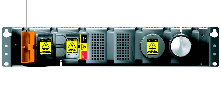
1X UBS Macro B T S FRU P ower Distribution Unit (PDU) Equipment Identication
Figure 1 -13 PDU rear panel detail
ti-cdma-05914.eps
CAUTION
CAUTION
CAUTION
1st Power Feed
+27 V DC Input
Power Connector
1st Power Feed
+27 V DC Input
Filter Capacitor
Location of Optional
2nd Power Feed
+27 V DC Input
Power Connector
NOTES:
1. Equipment shown is typical. The actual equipment appearance may vary slightly.
2. The optional 2nd power feed input connector is populated when more than 2 XMIs are equipped.
_
0 VDC
+
27 VD
C
HAZARD OF ELECTRICAL SHOCK WITH COVERS REMOVED
68P09283A64 -3 1 -43
FOA SEP 2007
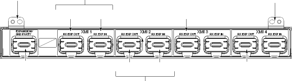
RX Splitter Equipment Identication Chapter 1: Ov erview
RX Splitter Equipment Identication■■■■■■■■■■■■■■■■■■■■■■■■■■■■■■■■■■■■■■■■■■■■■■■■■■■■■■■■■■■■■■
■
■
RX Splitter I/O Panel
Figure 1 -14 shows the wide band (800 MHz -to -2.1 GHz) RX splitter I/O panel.
Figure 1 -14 RX splitter front panel detail
WIDE BAND
RX SPLITTER
ti-cdma-06110.eps
Mounting
Tab Mounting
Tab
EXP OUT
(RX MAIN)
EXPANSION/
3RD PARTY
(Signal source via
splitter: RX MAIN is XMI 1
and RX DIV is XMI 2.)
NOTES:
1. All RX splitter connectors are ganged mini-coaxial.
2. RX EXP IN signal flow direction is from XMI.
RX EXP OUT signal flow direction is to XMI.
3. Used in both 1.9 GHz and 800 MHz multi-XMI
applications.
EXP IN
(RX DIV ) Future - XMI 3 EXP OUT
(RX MAIN & DIV)
Future - XMI 4 EXP OUT
(RX MAIN & DIV)
XMI 1
EXP IN
(RX MAIN)
EXP OUT
(RX DIV )
XMI 2
WIDE BAND SPLITTER
1 -44 68P09283A64 -3
FOA SEP 2007
1X UBS Macro B T S FRU P ower Supply Module (PSM) Shelf Equipment Identication
Power Supply Module (PSM) Shelf Equipment
Identication
■■■■■■■■■■■■■■■■■■■■■■■■■■■■■■■■■■■■■■■■■■■■■■■■■■■■■■■■■■■■■■
■
■
PSM I/O Panels
Figure 1 -15 shows I/O connectors and PSM slot locations on the front panel of the UBS Macro
BTS –48 V DC and 220 V AC PSM shelves. This figure also briefly describes connector usage.
A PSM will be used in PSM 3 slot when more +27 V DC output power is needed to support
additional equipment.
Figure 1 -16 shows I/O cable and connector locations on the rear panel of the UBS Macro BTS
—48 V DC PSM shelf . This figure also briefly describes cable and connector usage.
Figure 1 -17 shows I/O cable, connector and terminal locations on the rear panel of the UBS
Macro BTS 220 V AC PSM shelf . This figure also briefly describes cable and connector usage.
68P09283A64 -3 1 -45
FOA SEP 2007
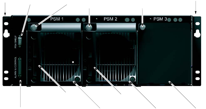
P ower Supply Module (PSM) Shelf Equipment Identication Chapter 1: Ov erview
Figure 1 -15 –48 V DC and 220 V AC PSM shelv es front panel detail
ti-cdma-05915.eps
Rack
Mounting
Flange
PSM SHELF
(9-pin sub-D Connector)
NOTE 1
AC or -48 V DC PSM Shelf
(front view) Rack
Mounting
Flange
ALARM & CONTROL
(50-pin Connector)
NOTE 2 Connects to ALARM
& CONTROL Connector on SSI
PSM 1 PSM 2 PSM 3
Empty Slot with
Blank Filler Panel
NOTES:
1. The PSM SHELF connector is only used when the UBS Macro frame is
equipped with two optional AC or -48 V DC PSM shelves. In this case, the
PSM SHELF connectors on the two PSM shelves are interconnected.
2. The ALARM & CONTROL connector connects to ALARM & CONTROL
connector on the SSI. If the UBS Macro frame is equipped with two optional
AC or -48 V DC PSM shelves, only one shelf has this connector cabled.
PSM Captive Retaining
Thumbscrew
Filler Panel Captive
Retaining Thumbscrew
PSM
Handle PSM
Handle
1 -46 68P09283A64 -3
FOA SEP 2007
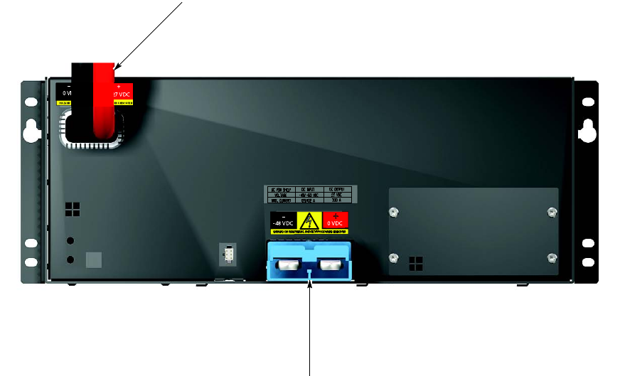
1X UBS Macro B T S FRU P ower Supply Module (PSM) Shelf Equipment Identication
Figure 1 -16 –48 V DC PSM shelf rear panel detail
_
-48 VDC 0 VD
C
_
0 VDC
+
27 V
DC
HAZARD OF ELECTRICAL SHOCK WITH COVERS REMOVED
ti-cdma-05916.eps
+27 V DC Output
Power Cable
(shown cut away)
To PDU
-48 VDC Input
Power Connector
(Blue)
68P09283A64 -3 1 -47
FOA SEP 2007
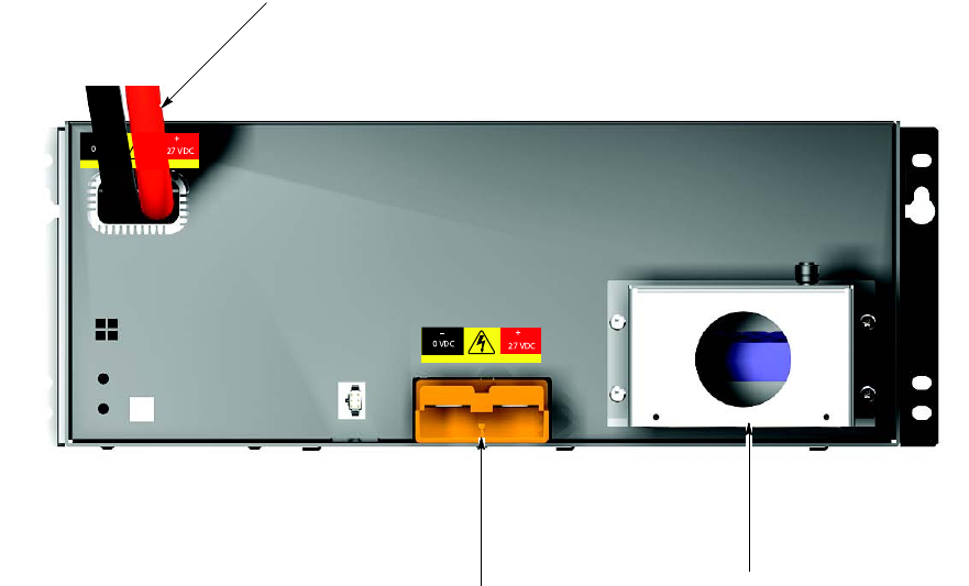
P ower Supply Module (PSM) Shelf Equipment Identication Chapter 1: Ov erview
Figure 1 -17 220 V AC PSM shelf rear panel detail
ti-cdma-05917.eps
+27 V DC Output
Power Connector
(Orange) Note 2
AC Input
Terminal Block
Protective Cover
NOTES:
1. Equipment shown is typical. The actual equipment appearance may vary slightly.
2. The +27 V DC Output connector may be connected to back-up batteries, but usage is optional.
+27 V DC Output
Power Cable
(shown cut away)
To PDU
_
0 VDC
+
27 VDC
HAZARD OF ELECTRICAL SHOCK WITH COVERS REMOVED
_
0 VDC
+
27 VDC
HAZARD OF ELECTRICAL SHOCK WITH COVERS REMOVED
1 -48 68P09283A64 -3
FOA SEP 2007

1X UBS Macro B T S FRU Optional RGPS Head Equipment Identication
Optional RGPS Head Equipment Identication■■■■■■■■■■■■■■■■■■■■■■■■■■■■■■■■■■■■■■■■■■■■■■■■■■■■■■■■■■■■■■
■
■
The information in this section of the manual will aid in identifying the optional RGPS head
equipment.
Any of the following RGPS heads may be used with the UBS Macro BTS:
•STLN6594 (Motorola part number)
•0186012H04 (Motorola part number)
The STLN6594 RGPS head is recommended and ships with the UBS Macro BTS when the
optional RGPS head is ordered.
The 0186012H04 RGPS head is an alternate and may be in use in the field as a replacement
spare.
Motorola recommends that the STLN6594 RGPS head be used as a replacement spare.
RGPS Head Mounting Method
The RGPS head is mounted outdoors on a pole. The pole is typically mounted to a wall. See
Figure 1 -18 for details.
68P09283A64 -3 1 -49
FOA SEP 2007
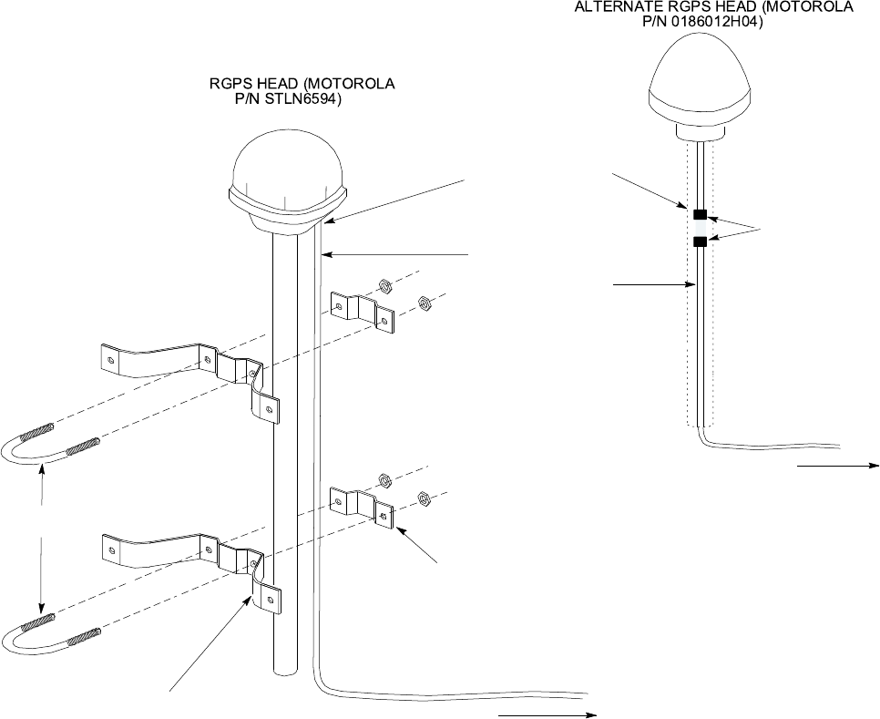
Optional RGPS Head Equipment Identication Chapter 1: Ov erview
Figure 1 -18 RGPS Head Mounting Details
Based on: ti-cdma-05740.eps
WALL MOUNTING
BRACKETS (2)
CLAMP BRACKETS (2)
U-BOLTS
CABLE TO LIGHTNING
ARRESTOR
RGPS HEAD WITH
12 PIN MALE
CONNECTOR
MATING
CONNECTORS
RGPS INTERFACE
CABLE WITH 12 PIN
FEMALE CONNECTOR
ON ONE END AND
UNTERMINATED WIRE
ON OTHER END
CABLE TO LIGHTNING
ARRESTOR
ALTERN ATE RGPS HEAD (MOTOR OLA
P/N 0186012H04)
RGPS H EAD (MOTORO LA
P/N STLN6594)
RGPS Head Details
The STLN6594 and 0186012H04 RGPS heads have similar connectors and threaded pole
mount adapters, but the implementation and location of these items varies between the two
heads (see Figure 1 -19 ).
1 -50 68P09283A64 -3
FOA SEP 2007
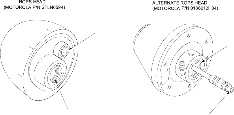
1X UBS Macro B T S FRU Optional RGPS Head Equipment Identication
Figure 1 -19 RGPS Head Equipment
ti-cdma-05702.eps
THREADED MOUNT
ADAPTER
THREADED MOUNT
ADAPTER 12-PIN DEUTSCH
TYPE MMP CONNECTOR
12-PIN DEUTSCH
TYPE MMP CONNECTOR
ALTERNATE RGPS HEAD
(MOTOROLA P/N 0186012H04)
RGPS HEAD
(MOTOROLA P/N STLN 6594)
68P09283A64 -3 1 -51
SEP 2007 FOA
Optional RGPS Head Equipment Identication Chapter 1: Ov erview
1 -52 68P09283A64 -3
FOA SEP 2007

C h a p t e r
2
Reference Procedures Performed At BTS Site■■■■■■■■■■■■■■■■■■■■■■■■■■■■■■■■■■■■■■■■■■■■■■■■■■■■■■■■■■■■■■
■
■
■
■
68P09283A64 -3 2 -1
SEP 2007 FOA
R eference Procedures P erformed at B T S Site Chapter 2: R eference Procedures P erformed A t B T S Site
Reference Procedures Performed at BTS Site■■■■■■■■■■■■■■■■■■■■■■■■■■■■■■■■■■■■■■■■■■■■■■■■■■■■■■■■■■■■■■
■
■
Introduction
The procedures in this chapter are referenced during various FRU replacement procedures
and are performed by the technician at the BTS site. These reference procedures include the
following:
•Frame power down and power -up sequence
2 -2 68P09283A64 -3
FOA SEP 2007

1X UBS Macro B T S FRU Fr ame P ower Down & P ower -Up Procedures
Frame Power Down & Power -Up Procedures■■■■■■■■■■■■■■■■■■■■■■■■■■■■■■■■■■■■■■■■■■■■■■■■■■■■■■■■■■■■■■
■
■
Powering Down the Frame
Prior to powering down the frame, perform the steps in Procedure 3 -2 Shutdown site
signaling functions procedure for a packet BTS on page 3 - 5 .
P ower down the frame by performing the steps in Procedure 2 -1 .
Procedure 2 -1 P owering Down the Fr ame
A T THE BTS SITE
1
Set all PDU DC circuit breakers to OFF (pulled out) in the following sequence (see
Figure 1-12 PDU front panel detail on page 1- 42 ):
•XMI 1 through XMI 4 (up to four breakers)
•DMI 1 through DMI 5 (up to five breakers)
•S SI 1 through S SI 2 (up to two breakers)
•ACC 1 through ACC 2 (up to two accessory breakers)
2
If the BTS site is equipped with backup batteries, set all battery circuit breakers to the
OFF position.
3
F or a +27 V DC powered UBS Macro frame, set the facility circuit breaker
controlling external +27 V DC power to the frame to the OFF position.
F or a — 48 V DC powered UBS Macro frame, set the facility circuit breaker
controlling external 48 V DC power to the PSM to the OFF position.
F or an AC powered UBS Macro frame, set the facility circuit breaker controlling
external AC power to the PSM to the OFF position.
Power -up the Frame
P ower -up the frame by performing the steps in Procedure 2 -2 .
68P09283A64 -3 2 -3
FOA SEP 2007

Fr ame P ower Down & P ower -Up Procedures Chapter 2: R eference Procedures P erformed A t B T S Site
Procedure 2 -2 P owering Up the Fr ame
A T THE BTS SITE
1
F or a +27 V DC powered UBS Macro frame, set the facility circuit breaker
controlling external +27 V DC power to the frame to the ON position.
F or a — 48 V DC powered UBS Macro frame, set the facility circuit breaker
controlling external 48 V DC power to the PSM to the ON position.
F or an AC powered UBS Macro frame, set the facility circuit breaker controlling
external AC power to the PSM to the ON position.
2
On the PDU , set the S SI circuit breakers to the ON position.
3
Check that the ST A TUS LED on the front panel of the each S SI is lighted.
4
F or BTSs with more than one DMI, during troubleshooting or for forcing one
DMI to synchronize code and data with the other DMI, it may be desired to
bring up a particular DMI as the site master . In this case, power up the DMI
that should be site master first, wait 1 minute, and then power up the other
DMI that should be non-site master . The non-site master DMI will synchronize
its code load and base file with the site master DMI.
On the PDU , set the DMI circuit breakers for all of the equipped DMIs to the ON position.
Circuit breakers for any DMIs that are not equipped, should be set to the OFF position.
5
Check that the ST LED on the front panel of each DMI is lighted.
6
Confirm that the DMI fans are on and operating by listening for fan motor hum and
feeling that air is being exhausted from the rear of the DMIs.
7
On the PDU , set the XMI circuit breakers to the ON position. There may be up to four
XMI circuit breakers; XMI 1 through XMI 4. Circuit breakers for any XMIs that are not
equipped, should be set to the OFF position.
8
Check that the ST/ALM LED on the front panel of each the XMI is lighted. Confirm that
the XMI fans are on and operating by listening for fan motor hum and feeling that air is
being exhausted from the rear of the XMI.
9
On the PDU , set the ACC circuit breakers to the ON position only if there are accessories
connected to the PDU otherwise set these breakers to the OFF position.
10
If the BTS site is equipped with backup batteries, set all battery circuit breakers to the
ON position.
A fter powering up the frame, perform the steps in Procedure 3 -3 Restore site
signaling operations procedure for a packet BTS on page 3 - 10 .
2 -4 68P09283A64 -3
FOA SEP 2007

C h a p t e r
3
Reference Procedures Performed At OMCR■■■■■■■■■■■■■■■■■■■■■■■■■■■■■■■■■■■■■■■■■■■■■■■■■■■■■■■■■■■■■■
■
■
■
■
68P09283A64 -3 3 -1
SEP 2007 FOA
R eference procedures performed at OMCR Chapter 3: R eference Procedures P erformed A t OMCR
Reference procedures performed at OMCR■■■■■■■■■■■■■■■■■■■■■■■■■■■■■■■■■■■■■■■■■■■■■■■■■■■■■■■■■■■■■■
■
■
Introduction
The procedures in this chapter are referenced during various FRU replacement procedures and
are performed by the OMCR operator . These reference procedures include the following:
•Accessing OMCR CLI window
•P acket BTS shutdown and restore procedures for BTS site
3 -2 68P09283A64 -3
FOA SEP 2007

1X UBS Macro B T S FRU Accessing OMCR CLI window
Accessing OMCR CLI window■■■■■■■■■■■■■■■■■■■■■■■■■■■■■■■■■■■■■■■■■■■■■■■■■■■■■■■■■■■■■■
■
■
Accessing OMCR CLI window
Many of the FRU procedures require the OMCR operator to manipulate BTS logical devices.
This is achieved using UNO or the OMCR (Operations and Maintenance Center - R adio)
Command Line Interface (CLI).
The operator enters commands using UNO or OMCR CLI.
The command dependent replacement procedures cannot be performed, if there are
any issues affecting the UNO or the OMCR CLI operations.
OMCR CLI access procedure
The following procedure is performed by the OMCR operator at the OMCR terminal.
Procedure 3 -1 Login and access alarm window procedure
1
Login to the OMCR by entering the user name.
2
Enter the password at the system prompt.
3
Type CLI at the system prompt to open an OMCR CLI window .
4
Open an UNO Alarm Manager (AM) window by performing the following:
1. Login to UNO as unoadmin
2. Set the env variable DISPLA Y to the IP address of the port where UNO
windows should be run.
3. Type uno & . The main UNO window that was set previously should
appear on the display .
4. Choose icon alarm manager from the main
uno window and set the appropriate filter
– OR –
choose Command Center icon -> BTS SDevices -> right click on
wanted bts icon and choose AlarmManager (filter will be set for
selected bts alarms).
5
V erify that the filter display is set to the BTS -# where the work is being
performed. This ensures that any BTS -# alarms, encountered while
installing the hardware, can be observed and rectified.
68P09283A64 -3 3 -3
FOA SEP 2007

P ack et B T S shutdown procedures Chapter 3: R eference Procedures P erformed A t OMCR
Packet BTS shutdown procedures■■■■■■■■■■■■■■■■■■■■■■■■■■■■■■■■■■■■■■■■■■■■■■■■■■■■■■■■■■■■■■
■
■
Shutdown site signaling functions for a packet BTS
If a complete site shutdown is required to support maintenance or upgrade operations, follow
Procedure 3 -2 to disable the packet BTS site.
This site shutdown procedure tak es the target B T S out -of -service (OOS) but does not
affect other B T Ss. T o minimiz e system impact, it ma y be advisable (but not necessary)
to perform this procedure during a maintenance window .
•The EDIT BTS REDIRECT or REDIRECT2 command does NOT affect calls in
progress and does NOT move these calls to another BTS . The command prevents
future calls from being originated on the targeted BTS and also redirects
subscribers to another site/carrier . If active call processing is still taking place
in the target BTS , wait for any active calls to terminate before locking/disabling
the BTS resources.
•Refer to the
System Commands Reference
manual for a complete explanation
of OMCR commands.
3 -4 68P09283A64 -3
FOA SEP 2007

1X UBS Macro B T S FRU P ack et B T S shutdown procedures
Procedure 3 -2 Shutdown site signaling functions procedure for a pack et B T S
At the OMCR
1
Open a CLI window . Refer to Accessing OMCR CLI window on page 3- 3 .
2
•The recommended shutdown technique is to redirect subscribers to
another site/carrier and then wait for any active calls to terminate before
locking/disabling the BTS .
•REDIRECT prevents future calls from being originated on the targeted
resource.
P erform one of the following:
•T o redirect subscribers and then wait for any active calls to terminate before disabling
the BTS , go to step 3 .
•T o lock/disable the BTS when there is no concern for redirecting subscribers and
waiting for any active calls to terminate, perform step 23 through step 26 only .
3
The REDIRECT command is used to invoke the REDIRECT2 command which is then
used to redirect subscribers to a different CDMA carrier frequency . REDIRECT2 is
the preferred command if an alternate CDMA carrier is available.
Enter the following command at the prompt to display the status of the BTS signaling redirect
parameters for all carriers equipped for the BTS:
omc-000000> DISPLAY BTS-<bts#> REDIRECT
4
Record the values shown in the system display response resulting from performing step 3 .
These values are needed to answer the prompts for the EDIT BTS REDIRECT
command when restoring signaling operations at the end of the maintenance or
upgrade procedure.
Continued
68P09283A64 -3 3 -5
FOA SEP 2007

P ack et B T S shutdown procedures Chapter 3: R eference Procedures P erformed A t OMCR
Procedure 3 -2 Shutdown site signaling functions procedure for a pack et B T S
(Continued)
5
This step edits the REDIRECT parameters so that the Global Service Redirect
Message to be broadcast on the paging channel redirects all subscribers away from
the BTS and onto a different BTS or system.
Enter the following command at the prompt:
omc-000000> EDIT BTS-<bts#> REDIRECT!
The system prompts to enter each command parameter value one at a
time. Answer the prompts in the following order with the entries shown:
<accolc0> enter Y,<accolc1> enter Y,...<accolc15> enter Y
(All Access Overload Classes must be set to yes to ensure that all subscribers are redirected.)
<returniffail> enter N
(Must be set to no to ensure that subscribers do not return if redirect is unsuccessful.)
<recordtype> enter 1or 2
(A value of 2 will invoke REDIRECT2 which is used to
redirect subscribers to a CDMA channel at a neighbor site.
<expectedsid> enter 13
(Use the Area ID the subscriber units should expect to find on the system where they are
being redirected. This example uses 13. The valid range is 0–32767; the default is 0.)
<ignorecdma> enter Y
<sysordering> enter CUSTOM
(The system acquisition ordering value tells the mobiles the order to use when attempting to
obtain service on the different analog systems. V alid values are:
•CUSTOM — use custom system selection
•AONL Y — try the A system only
•B ONL Y — use the B system only
•AFIRST — try the A system first. If unsuccessful, try the B system
•BFIRST — try the B system first. If unsuccessful, try the A system
•AORB — try A or B. If unsuccessful, try the alternative system
CUSTOM is the default.)<rotatetimer> enter 4
(Call processing continuously rotates in circular right-shifts, the Y/N values of Access
Overload Class Redirect Flags 0 to 9. V alues are shifted one flag at the end of the timer
period; then timer restarts. V alid values are 0–255; 4 is the default.)
Continued
3 -6 68P09283A64 -3
FOA SEP 2007

1X UBS Macro B T S FRU P ack et B T S shutdown procedures
Procedure 3 -2 Shutdown site signaling functions procedure for a pack et B T S
(Continued)
6
A fter all parameters are entered, the system displays the command to
be sent and the prompt below . V erify the command syntax is correct.
omc-000000>Accept [yes/no]?
7
A t the prompt shown in step 6 , enter Yto accept the command or Nto go bottom and enter
the correct value(s).
8
Enter the following command at the prompt to display the status of the signaling REDIRECT
parameters to verify that the applicable BTS is ready for global redirect:
omc-000000> DISPLAY BTS-<bts#> REDIRECT
9
Ensure that the values in the system display response match the values input in step 5 .
10
Enter the following command at the prompt to display the status of the BTS signaling redirect
parameters for all carriers equipped for the BTS:
omc-000000> DISPLAY BTS-<bts#> REDIRECT2
1 1
Record the values shown in the system display response resulting from step 10 .
These values are used to answer the prompts for the EDIT BTS REDIRECT2
command when restoring signaling operations at the end of the replacement
procedure.
12
This step edits the REDIRECT2 parameters so that the Global Service Redirect
Message to be broadcast on the paging channel redirects all subscribers away from
the BTS with the failed equipment and onto a CDMA channel at a neighbor site.
Enter the following command at the prompt:
omc-000000> EDIT BTS-<bts#> REDIRECT2!
The system prompts to enter each command parameter value one at a time. Answer the
prompts in the following order:
expecting an integer number (from 0 to 65535)
<EXPNID= ?>
Continued
68P09283A64 -3 3 -7
FOA SEP 2007

P ack et B T S shutdown procedures Chapter 3: R eference Procedures P erformed A t OMCR
Procedure 3 -2 Shutdown site signaling functions procedure for a pack et B T S
(Continued)
(Use the Network ID the subscriber units should expect to find on the system they are
being redirected to .)
expecting an integer number (from 0 to 2047)
<chan1= ?>, <chan2= ?> . . . <chan15= ?>
(A list of CDMA channels for neighbor sites that the subscriber units can use for redirection.)
expecting an enumerated value:
CDMA1900 CDMA2100 CDMA800 CDMA900 JAPANCDMA
<BANDCLASS= ?>
(Use CDMA1900 for 1900 MHz systems, CDMA2100 for 2100 MHz systems, and CDMA800
for 800 MHz systems. This example uses 1900 MHz.)
13
A fter all parameters are entered, the system displays the command to be sent and the prompt
below . V erify the command syntax is correct.
omc-000000>Accept [yes/no]
14
A t the prompt shown in step 13 , enter Yto accept the command or Nto go bottom and
enter the correct value(s).
15
Enter the following command at the prompt to display the status of the BTS signaling
REDIRECT2 parameters to verify that the BTS is ready for maintenance:
omc-000000> DISPLAY BTS-<bts#> REDIRECT2
16
Ensure that the values in the system display response match the values input in step 12 .
17
Enter the following command at the prompt to display the existing congestion control
parameters for all carriers equipped for the BTS:
omc-000000> DISPLAY BTS-<bts#> CONGESTCONF
18
This step edits the value of the Global Service Redirection Flag ( GLOBALREDIRECT )
in the congestion control parameters so that the Global Service Redirect Message
is broadcast on all of the sector paging channels at the BTS .
Enter the following command at the prompt using the applicable BTS number:
omc-000000> EDIT BTS-<bts#> CONGESTCONF!
Continued
3 -8 68P09283A64 -3
FOA SEP 2007

1X UBS Macro B T S FRU P ack et B T S shutdown procedures
Procedure 3 -2 Shutdown site signaling functions procedure for a pack et B T S
(Continued)
19
The system prompts to enter each control parameter value one at a time. Skip through the
prompts until reaching the following, and enter the parameter shown:
<globalredirect> ENABLE
(This will force the Global Service Redirect Message to be broadcast on all of the sector
paging channels at the BTS .)
20
When the system displays the values of the control parameters and the following prompt,
verify that only the GLOBALREDIRECT value changed.
omc-000000>Accept [yes/no]?
21
If only the GLOBALREDIRECT value changed, enter Yto accept the change.
(When the change is accepted, the Global Service Redirection Message is sent over the sector
paging channels. All subscribers are redirected away from the BTS and onto a different
system or CDMA carrier channel. This effectively shuts down the BTS .)
22
V erify that the CONGESTCONF Global Redirect is enabled for each carrier at the BTS by entering
the following command at the prompt:
omc-000000> DISPLAY BTS-<bts#> CONGESTCONF
23
Enter the following command at the prompt to display the status of all devices at the BTS:
omc-000000> DISPLAY BTS-<bts#> STATUS
24
Record all devices that are listed as OOS_AUTOMATIC in the response to step 23 .
This information will be used for later reference when restoring site signaling
operations.
25
W ait for three minutes to allow any active calls to terminate then go the next step.
26
Lock/disable the BTS by entering either of the following commands at the prompt:
•omc-000000> DISABLE BTS-<bts#> UNC
•omc-000000> LOCK BTS-<bts#>
68P09283A64 -3 3 -9
FOA SEP 2007

P ack et B T S start -up procedures Chapter 3: R eference Procedures P erformed A t OMCR
Packet BTS start -up procedures■■■■■■■■■■■■■■■■■■■■■■■■■■■■■■■■■■■■■■■■■■■■■■■■■■■■■■■■■■■■■■
■
■
Restore site signaling operations for a packet BTS
Restore site signaling operations according to Procedure 3 -3 .
Procedure 3 -3 R estore site signaling oper ations procedure for a pack et B T S
At the OMCR
1
Open a CLI window . Refer to Accessing OMCR CLI window on page 3- 3 .
2
Unlock/enable the BTS by entering either of the following commands at the prompt:
•omc-000000> ENABLE BTS-<bts#> UNC
•omc-000000> UNLOCK BTS-<bts#>
3
V erify that the system automatically returns a Network Element State Change Event
message for the BTS . These messages show the old and new states for the devices. The new
state should be UNLOCKED/ENABLED/ACTIVE .
4
Display the status of all devices at the BTS by entering the following command at the prompt:
omc-000000> DISPLAY BTS-<bts#> STATUS
5
Examine the response to make sure there are not more OOS_AUTOMATIC devices than were
recorded in step 24 of Procedure 3-2 .
Devices that were previously OOS_AUTOMATIC may now be INS .
6
P erform one of the following depending on redirection actions taken in Procedure 3-2 :
•If subscribers were not redirected according to the steps in Procedure 3-2 , stop here.
•If subscribers were redirected according to Procedure 3-2 , perform the remaining
steps of this table.
7
Enter the following command at the prompt to display the congestion control parameters for
all carriers equipped for the BTS:
omc-000000> DISPLAY BTS-<bts#> CONGESTCONF
Continued
3 -10 68P09283A64 -3
FOA SEP 2007

1X UBS Macro B T S FRU P ack et B T S start -up procedures
Procedure 3 -3 R estore site signaling oper ations procedure for a pack et B T S
(Continued)
8
This step edits the value of the Global Service Redirection Flag ( GLOBALREDIRECT )
in the congestion control parameters so that the Global Service Redirect Message
is only broadcast on the sector paging channel when there is traffic congestion
in the sector
Enter the following command at the prompt using the applicable BTS number:
omc-000000> EDIT BTS-<bts#> CONGESTCONF !
9
The system prompts to enter each control parameter value one at a time. Skip through the
prompts until reaching the following, and enter the parameter shown:
<globalredirect> DISABLE
(This will revert the Global Service Redirect Message to congestion control.)
10
When the system displays the values of the control parameters and the following prompt,
verify that only the GLOBALREDIRECT value changed.
omc-000000>Accept [yes/no]?
11
If only the GLOBALREDIRECT value changed, enter Yto accept the change.
(Now the Global Service Redirection Message will only be sent over the sector paging
channels when there is traffic congestion in the sector .)
12
V erify that the CONGESTCONF globalredirect is disabled for each carrier at the BTS by
entering the following command at the prompt:
omc-000000> DISPLAY BTS-<bts#> CONGESTCONF
13
Display the status of the signaling REDIRECT parameters for all carriers equipped for the
applicable BTS by entering the following command at the prompt:
omc-000000> DISPLAY BTS-<bts#> REDIRECT
14
Examine the values in the system display response to be sure they match the values input in
step 5 of Procedure 3-2 .
Continued
68P09283A64 -3 3 -11
FOA SEP 2007

P ack et B T S start -up procedures Chapter 3: R eference Procedures P erformed A t OMCR
Procedure 3 -3 R estore site signaling oper ations procedure for a pack et B T S
(Continued)
15
In this step, use the values recorded in step 4 of Procedure 3-2 to answer the
prompts for the EDIT BTS REDIRECT command, except for <recordtype> , enter 2.
Restore the values of all REDIRECT parameters by entering the following command at the
prompt:
omc-000000> EDIT BTS-<bts#> REDIRECT !
The system prompts to enter each command parameter one at a time. Answer the
prompt in the following order:
The following specified values are consistent with the original example. Actual
values may vary .
<accolc0> enter N,<accolc1> enter N, . . . <accolc15> enter N
<returniffail> enter N
<recordtype> enter 2
<expectedsid> enter 0
<ignorecdma> enter N
<sysordering> enter CUSTOM
<rotatetimer> enter 4
16
A fter all parameters are entered, the system displays the command to be sent and the prompt
below . V erify the command syntax is correct.
omc-000000>Accept [yes/no]?
17
A t the prompt shown in step 16 , enter Yto accept the command or Nto go bottom and enter
the correct value(s).
18
Enter the following command at the prompt to display the status of the signaling REDIRECT
parameters:
omc-000000> DISPLAY BTS-<bts#> REDIRECT
19
Ensure that the values in the system display response matches with the values input by the
operator in step 15 .
3 -12 68P09283A64 -3
FOA SEP 2007

C h a p t e r
4
E -GPS (External -GPS) Replacement
Procedures
■■■■■■■■■■■■■■■■■■■■■■■■■■■■■■■■■■■■■■■■■■■■■■■■■■■■■■■■■■■■■■
■
■
■
■
68P09283A64 -3 4 -1
SEP 2007 FOA

E -GPS (External -GPS) Chapter 4: E -GPS (External -GPS) R eplacement Procedures
E -GPS (External -GPS)■■■■■■■■■■■■■■■■■■■■■■■■■■■■■■■■■■■■■■■■■■■■■■■■■■■■■■■■■■■■■■
■
■
E -GPS Description
The E -GPS is located in the UBS Macro BTS frame and is mounted at the very top of the frame.
The E -GPS may be used instead of the optional Remote GPS (RGPS) head.
The E -GPS contains a GPS Receiver (GPSR) that requires connection to an external GPS RF
antenna signal. The E -GPS is considered to be local with respect to the UBS Macro BTS frame,
while the RGPS head is remotely located with respect to the UBS Macro BTS frame.
All cable connections to the E -GPS are made on the E -GPS front panel (see Figure 1 -4 E -GPS
I/O Details on page 1 - 31 ).
The E -GPS S SI -GPS connector is cabled to the S SI RGPS connector . This connection allows the
UBS Macro BTS frame to supply DC power to the E -GPS . In addition, control/data signals are
exchanged between the DMI controller and the E -GPS via this connection.
The E -GPS GPS -ANT connector is cabled to the external GPS RF antenna cable connector . This
coaxial cable connection allows the E -GPS to receive RF signals from GPS satellites as well as
supply DC power to the GPS RF antenna preamplifiers.
The E -GPS receiver successfully tracks and acquires GPS satellites. The receiver detects GPS
RF signals and extracts a 1 Pulse P er Second (1PPS) timing signal. This 1PPS signal is applied
to the DMI controller via the S SI -GPS connector . The DMI controller contains an internal
Motorola Stability Oscillator (MSO) that is synchronized to the 1PPS timing signal and locked
to the GPS time base. If satellite tracking is lost or if the E -GPS fails, the MSO free runs, but
can maintain system timing for up to 8 hours.
If the UBS Macro BTS frame is equipped with an optional Quartz High Stability Oscillator
(QHSO), the DMI controller selects the QHSO as the backup synchronization source instead of
the MSO . The QHSO can maintain system timing for up to 24 hours.
System Impact/Considerations
P erforming this replacement procedure should not require BTS downtime or impact
call processing because of MSO or QHSO backup. However E -GPS downtime will
occur . And alarms will be reported.
4 -2 68P09283A64 -3
FOA SEP 2007

1X UBS Macro B T S FRU E -GPS (External -GPS)
A failed E -GPS should be replaced immediately after failure detection and within
the applicable MSO/QHSO backup time period (i.e., up to 8 hours MSO and up to
24 hours QHSO).
A fter the replacement E -GPS is re -connected and powered up, it may take up to 30
minutes for the replacement E -GPS to successfully track and acquire satellites.
Table 4 -1 FRU R eplacement Conditions
FRU
Ref Designator What to Shut Down...
E -GPS E -GPS
Nothing; FRU is hot swappable and BTS
system timing is backed up by either MSO
(for up to 8 hours) or QHSO (for up to 24
hours).
Required Items
Documents
•
1X UBS Macro BTS Optimization/A TP manual
Tools
•T25 TORX bit
•T orque driver
Torque Requirements
•M5 thumbscrew - 4.77 N -m (42 in -lb)
Replacement Unit
•E -GPS (Motorola model ST TG4052)
68P09283A64 -3 4 -3
FOA SEP 2007

E -GPS (External -GPS) Chapter 4: E -GPS (External -GPS) R eplacement Procedures
Prerequisite
Before You Begin
Before you begin, record the pertinent information in the following table (see T able 4 -2 ):
Table 4 -2 Item Number R eplacement List
Item
Number
BTS number
F ailed E -GPS number
E -GPS Replacement Procedure
P erform the steps in Procedure 4 -1 to replace the E -GPS .
Procedure 4 -1 E -GPS R eplacement Procedure
A T THE BTS SITE
1
Disconnect all cables from the E -GPS front panel. If desired, tag all cables prior to
disconnecting them. Move cables out of the way .
2
Using a T25 TORX bit and driver , loosen the thumbscrew on the module front panel. Using
your thumb and finger , completely loosen the captive thumbscrew .
3
Pull up on the thumbscrew to start removing the module. Then grasp the module front panel
and pull the module completely out of the E -GPS mounting bracket.
4
W ith the replacement module properly positioned in front of the E -GPS mounting bracket,
align the module bottom side rails with the guide channels of the mounting bracket. Slide the
module completely into the mounting bracket.
5
Align the module thumbscrew with the threaded hole in the mounting bracket. Using a T25
TORX bit and driver , tighten the thumbscrew to 4.77 N-m (42 in-lb).
6
Reconnect all cables to the E -GPS front panel.
A fter the replacement E -GPS is re-connected and powered up, it may take up to 30
minutes for the replacement E -GPS to successfully track and acquire satellites.
7
If optimization is to be performed at this time, see Optimization Required
following this table.
4 -4 68P09283A64 -3
FOA SEP 2007
1X UBS Macro B T S FRU E -GPS (External -GPS)
Optimization Required
Consult the
1X UBS Macro BTS Optimization/A TP manual
for the following optimization/test
instructions:
•Timing Initialization/V erification
•BTS Device Database Audit
•BTS Device Database Update
68P09283A64 -3 4 -5
SEP 2007 FOA
E -GPS (External -GPS) Chapter 4: E -GPS (External -GPS) R eplacement Procedures
4 -6 68P09283A64 -3
FOA SEP 2007

C h a p t e r
5
IDRF Replacement Procedure■■■■■■■■■■■■■■■■■■■■■■■■■■■■■■■■■■■■■■■■■■■■■■■■■■■■■■■■■■■■■■
■
■
■
■
68P09283A64 -3 5 -1
SEP 2007 FOA

IDRF (Integr ated Duplex er RX Filter) Chapter 5: IDRF R eplacement Procedure
IDRF (Integrated Duplexer RX Filter)■■■■■■■■■■■■■■■■■■■■■■■■■■■■■■■■■■■■■■■■■■■■■■■■■■■■■■■■■■■■■■
■
■
IDRF Description
The IDRF is available in either the 800 MHz or 1.9 GHz RF band.
The IDRF (Integrated Duplexer RX Filter) includes:
•TX/RX bandpass filters
•Bi -directional TX and RX antenna path couplers.
The IDRF is a passive device requiring no DC input operating power .
The IDRF allows the sector TX and main RX RF carrier signals to share the same antenna. It
also allows connection for a sector diversity RX RF antenna. The bi -directional antenna couplers
provide forward and reflected signal port connections for antenna signal sampling and signal
injection. The coupled ports are typically used for connection to test equipment.
The UBS Macro BTS frame is typically equipped with one IDRF per sector . Figure 1 -2 Low
capacity UBS Macro BTS starter frame (1800 mm rack) on page 1 - 28 and Figure 1 -3 UBS
Macro BTS mid -capacity frame (1800 mm rack) on page 1 - 30 show the location of the IDRFs
within the UBS Macro frame.
Figure 1 -5 800 MHz IDRF I/O Details on page 1 - 32 and Figure 1 -6 1.9 GHz IDRF I/O Details on
page 1 - 33 show the locations of IDRF RF I/O port connectors.
System Impact/Considerations
P erforming this replacement procedure will cause downtime for all XMIs which will
suspend all call processing for the BTS .
The removal of a failed IDRF requires that all XMIs be dekeyed.
All of the XMIs will be disabled/locked to ensure that the transmitters are dekeyed. This will
interrupt all TX RF sector carriers.
Removal of the IDRF interrupts the associated sector TX/RX antenna paths.
Alarms will be reported during the replacement procedure.
A fter replacing an IDRF , the associated sector RX/TX paths must be optimized following the
procedure listed in the
1X UBS Macro BTS Optimization/A TP
manual.
5 -2 68P09283A64 -3
FOA SEP 2007

1X UBS Macro B T S FRU IDRF (Integr ated Duplex er RX Filter)
Table 5 -1 IDRF R eplacement Conditions
FRU
Ref Designator What to Shut Down...
Integrated
Duplexer RX Filter
IDRF 1, 2, 3 (TX/RX
main antenna & RX
diversity; sectors 1,
2, 3)
From the OMCR, lock all XMIs.
Required Items
Documents
•
1X UBS Macro BTS Optimization/A TP
manual.
Tools
•T25 TORX bit
•T orque driver
•19 mm open -end wrench (for N -type connectors)
•SMA break over wrench - 1.02 N -M (9 in -lb)
Torque Requirements
•M5 mounting screws - 4.77 N -m (42 in -lb)
Replacement Unit
•China Full Band 800 MHz IDRF (Motorola model STFN4009)
•India Full Band 800 MHz IDRF (Motorola model STFN4010)
•US Full Band 800 MHz IDRF (Motorola model STFN4015)
•US A -band 800 MHz IDRF (Motorola model STFN4016)
•US B -band 800 MHz IDRF (Motorola model STFN4017)
•1.9 GHz IDRF (Motorola model STFG4055)
68P09283A64 -3 5 -3
FOA SEP 2007

IDRF (Integr ated Duplex er RX Filter) Chapter 5: IDRF R eplacement Procedure
Prerequisite
Coordinate this repair task with the OMCR operator .
Before You Begin
Record the pertinent information in T able 5 -2 .
Table 5 -2 Item Number R eplacement List
Item
Number
BTS
F ailed IDRF number
IDRF Replacement Procedure
This procedure requires working on or around circuitry extremely sensitive to ESD .
W ear a conductive, high impedance wrist strap during the procedure.
F ollow appropriate safety measures.
P erform the procedures in Procedure 5 -1 to replace a failed IDRF .
Procedure 5 -1 R eplacing an IDRF
A T THE OMCR
1
Open a CLI window . Refer to Accessing OMCR CLI window on page 3- 3 .
2
It will be helpful if the OMC-R operator executes “ENABLE EVENTS" command at the CLI
session of the OMC-R to monitor alarms. This command is optional and may not be useful if
executed during a high CP U utilization time.
Continued
5 -4 68P09283A64 -3
FOA SEP 2007

1X UBS Macro B T S FRU IDRF (Integr ated Duplex er RX Filter)
Procedure 5 -1 R eplacing an IDRF (Continued)
The OMCR operator must lock all XMIs before the failed IDRF can be removed.
3
Lock each XMI by entering the following command at the prompt:omc-000000> LOCK XMI-<bts#>-<xmi#> UNC
4
Display the status of each XMI, by entering the following command at the prompt:omc-000000> DISPLAY BTS-<bts#> STATUS
V erify that each XMI is in an OOS_MANU AL state.
A T THE BTS SITE
5
W orking at the top front of the UBS Macro BTS frame, tag and disconnect all cables from the
front of failed IDRF . Move cables out of the way .
6
Using a T25 TORX driver , remove the four screws that secure the IDRF to the IDRF shelf .
There is one screw at each corner of the IDRF mounting plate.
7
Grasp the IDRF . Lift it up and out of the of the IDRF shelf .
8
Disconnect all cables from the bottom of the failed IDRF .
9
Reconnect all cables to the bottom of the replacement IDRF .
10
P osition the replacement IDRF in the proper orientation and insert it into the IDRF shelf .
11
Secure the replacement IDRF to the IDRF shelf with the four mounting screws. Using a T25
TORX driver , tighten the mounting screws to 4.77 N-m (42 in-lb).
12
Reconnect all cables to the replacement IDRF .
13
This completes the physical installation of the FRU . If optimization is to be performed at this
time, see Optimization required following this table.
A T THE OMCR
14
Unlock each XMI by entering the following command at the prompt:omc-000000> UNLOCK XMI-<bts#>-<xmi#> UNC
15
Display the status of each XMI by entering the following command at the prompt:omc-000000> DISPLAY BTS-<bts#> STATUS
V erify that each XMI is in an INS_ACTIVE state.
16
From the OMCR, monitor the Alarm Manager . V erify that old alarms are cleared and no
new alarms are reported.
Optimization Required
P erform the following BTS Optimization/A TP procedures for the affected sector:
•TX P ath Calibration Audit
•RS SI T est (FER T est is optional)
Refer to the
1X UBS Macro BTS Optimization/A TP
manual.
68P09283A64 -3 5 -5
SEP 2007 FOA
IDRF (Integr ated Duplex er RX Filter) Chapter 5: IDRF R eplacement Procedure
5 -6 68P09283A64 -3
FOA SEP 2007

C h a p t e r
6
SSI Replacement Procedures■■■■■■■■■■■■■■■■■■■■■■■■■■■■■■■■■■■■■■■■■■■■■■■■■■■■■■■■■■■■■■
■
■
■
■
68P09283A64 -3 6 -1
SEP 2007 FOA
S SI (Site Span I/O) Module Chapter 6: S SI R eplacement Procedures
SSI (Site Span I/O) Module■■■■■■■■■■■■■■■■■■■■■■■■■■■■■■■■■■■■■■■■■■■■■■■■■■■■■■■■■■■■■■
■
■
SSI Description
The first instance of the S SI is located in the right, front side of the IDRF shelf of the UBS
Macro BTS Frame. F or S SI location, refer to the applicable Figure 1 -1 UBS Macro BTS
low -tier/low -capacity frame (1000 mm rack) on page 1 - 27 through Figure 1 -3 UBS Macro BTS
mid -capacity frame (1800 mm rack) on page 1 - 30 .
F or S SI connector identification, refer to Figure 1 -7 S SI front panel details on page 1 - 35 and
Figure 1 -8 S SI rear panel details on page 1 - 36 .
The S SI housing has a built -in mounting mechanism (see Figure 1 -8 S SI rear panel details on
page 1 - 36 ). This mounting mechanism allows the S SI to be mounted in the appropriate shelf .
One end of the S SI housing has two hooks that engage with two slots on the appropriate shelf .
The opposite end of the S SI housing has a right angle flange with two thumbscrews that secure
the S SI to the appropriate shelf .
The S SI operates from +27 V DC power supplied from a PDU S SI power connector that is
cabled to the POWER IN connector on the front of the S SI. A PDU S SI 20A circuit breaker
controls DC input power for the S SI.
The S SI contains I/O interface circuitry between the DMI and ancillary/external electronic
equipment. The specific equipment I/O and S SI connectors are as follows:
6 -2 68P09283A64 -3
FOA SEP 2007

1X UBS Macro B T S FRU S SI (Site Span I/O) Module
•E -GPS module I/O or RGPS head I/O or GPS Synch Sharing Input — RGPS 15 -pin connector
(DC operating power to the E -GPS module/RGPS head is provided via this connector).
•Buffered BTS system time synchronize signal output for daisy chaining multiple frames at
a BTS site to a common synchronization source — SYNC SHARING 15 -pin connector .
•External 10 MHz frequency reference input — EXT REF IN BNC connector .
•Frequency reference output to test equipment — FREF OUT BNC connector .
•Time reference output to test equipment — TREF OUT BNC connector .
•ALARM/CONTROL Connector on Optional PSM Shelf — PSM 50 -pin connector .
•Customer alarm input/output devices (up to 24 inputs & up to 8 outputs) — CUSTOMER IP
1 -12 OP 1 -4 and CUSTOMER IP 13 -24 OP 5 -8 two 37 -pin connectors.
•10/100 BaseT Ethernet serial data for connection of LMF or other equipment — CRMS/LMT
CUSTOMER ENET RJ -45 connector .
•IP -packet backhaul, using one of the following connection methods:
Span I/O for T1/E1 balanced — SP AN 37 -pin connector .
Optional Span I/O for E1 unbalanced daughter card to SP AN 37 -pin connector — 16
BNC connectors, 2 per Span, RX and TX.
Open Transport Interface (OTI) — two, BACKHAUL ENET , 10/100 BaseT Ethernet
RJ -45 connectors.
•QHSO module I/O — HSO 9 -pin connector (DC operating power to the QHSO is provided
via this connector).
System impact/considerations
P erforming this replacement procedure will cause BTS downtime and impact call
processing.
The S SI is non -redundant. Alarms will be generated during the S SI replacement procedure.
The S SI is not hot swappable.
68P09283A64 -3 6 -3
FOA SEP 2007

S SI (Site Span I/O) Module Chapter 6: S SI R eplacement Procedures
S SI removal requires powering off the S SI and disconnecting all of its cables. Operation of
the following will be interrupted:
•E -GPS or RGPS whichever is applicable.
•QHSO
•ALARM/CONTROL for the optional PSM shelf
•LMF
•Customer alarm input/output devices
•IP -packet backhaul
The DMI controller will switchover to the DMI MSO as a backup reference source.
Call traffic processing through the site will be interrupted by the S SI replacement procedure.
Alarms will be reported.
Table 6 -1 S SI R eplacement Conditions
FRU
Ref Designator What to Shutdown...
Site Span I/O
Module
S SI
Shutdown site signaling functions and DC
operating power to the S SI.
SSI LEDs
The following bi -color LED indicators are located on the S SI front panel by the DMI and RJ -45
connectors (see ):
•ALARM
•INST ANCE
•ST A TUS
T able 6 -2 shows the possible states for the S SI front panel LEDs and the corresponding
indication.
Table 6 -2 S SI LEDs States and Indications
ALARM LED State INST ANCE LED State ST A TUS LED State
Indication
Off Off Off
No DC P ower to FRU
On Orange On
LED Indicator T est (temporary; 0.5 sec
to 1 sec)
On
N/A
Off FRU F ailure
Off
N/A N/A
No FRU F ailure
Continued
6 -4 68P09283A64 -3
FOA SEP 2007

1X UBS Macro B T S FRU S SI (Site Span I/O) Module
Table 6 -2 S SI LEDs States and Indications (Continued)
ALARM LED State INST ANCE LED State ST A TUS LED State
Indication
Flashing
(1.5 sec-On/1
sec-Off)
N/A N/A
P artial (soft) FRU F ailure
N/A N/A
Flashing
(250 ms-On/250
ms-Off)
FRU Booting up (not active)
N/A N/A
On FRU Active
N/A
Green Flashing
(0.5 sec-On/0.5
sec-Off cycle count)
followed by 3
sec-Off
N/A
Instance Indicator and No FRU
Cabling Connection Errors Detected.
Cycle count equals FRU type instance;
where: 1 flash = 1st instance, 2 flashes
= 2nd instance, 3 flashes = 3rd instance,
so on and so forth.
N/A
Red
N/A
FRU Cabling Connection Error Detected
N/A = LED state is Not Applicable to indication
Required items
Documents
•
1X UBS Macro BTS Optimization/A TP
manual.
Tools
•T orque driver
•T25 TORX driver
•T20 TORX driver
Torque requirements
•S SI mounting bracket thumbscrews, optional E1 daughter card mounting screws, and
optional QHSO thumbscrew – 2.37 N -m (21 in -lb)
Replacement unit
•S SI (Motorola model STLN6390)
68P09283A64 -3 6 -5
FOA SEP 2007
S SI (Site Span I/O) Module Chapter 6: S SI R eplacement Procedures
Prerequisite
Coordinate this repair task with the OMCR operator .
Before you begin
Before you begin, enter the information into the following replacement list table.
Table 6 -3 Item Number R eplacement List
Item Number
BTS number
F ailed S SI number
SSI replacement procedure
This procedure requires working on or around circuitry which is extremely sensitiv e
to ESD . W ear a conductiv e, high impedance wrist str ap during the procedure. Use
appropriate safet y measures.
F or frames with more than one DMI — during the time that the S SI is powered
off or not connected to the DMIs, the DMIs will be rebooting continuously to try
to re -establish communication with the S SI. T o minimize the number of reboots
that could eventually cause the DMIs to swap partitions to an older code load (i.e.,
10 reboots), perform the "A T THE BTS SITE" portions of Procedure 6 -1 and then
Procedure 6 -2 within 5 minutes. If this is not possible, it is recommended to power
off all DMIs when the S SI is powered off . Then, power the DMIs back up after the
new S SI is powered up.
T o replace the S SI perform Procedure 6 -1 and then Procedure 6 -2 .
6 -6 68P09283A64 -3
FOA SEP 2007
1X UBS Macro B T S FRU S SI (Site Span I/O) Module
Procedure 6 -1 R emo ving the failed S SI
A T THE OMCR
1
Shut down site signaling functions according to Procedure 3-2 Shutdown site signaling
functions procedure for a packet BTS on page 3- 5 .
A T THE BTS SITE
2
P ower down the S SI by setting the corresponding PDU S SI 20A circuit breaker to the off
position (pulled out).
Mak e sure the PDU S SI circuit break er is set to OFF .
Y ou will be disconnecting multiple cables from connectors. If necessary , use
masking tape and a marker and temporarily tag each cable as to the proper
connector before disconnection.
3
Disconnect all of the cables connected to the S SI front panel connectors.
4
Use a T25 TORX bit/driver to completely loosen the two captive thumbscrews on the S SI
bracket right angle flange. Disengage the thumbscrews from the mounting shelf .
5
Grasp the S SI bracket right angle flange. Slide the S SI toward the middle of the mounting
shelf until the S SI bracket hooks are disengaged from the two slots on the shelf . Pull the
S SI out of the shelf .
6
If the S SI is equipped with an optional E1 daughter card. Transfer the E1 daughter card from
the failed S SI to the replacement S SI by performing step 3 through step 7 in Procedure 6-3
Replacing the E1 daughter card on page 6- 11 .
7
If the S SI is equipped with an optional QHSO . Transfer the QHSO from the failed S SI to
the replacement S SI by performing step 5 through step 10 in Procedure 6-4 Replacing
the QHSO on page 6- 15 .
Procedure 6 -2 Installing the replacement S SI
A T THE BTS SITE
1
Properly position the S SI so that the two hooks on the S SI bracket are engaged in the two
slots on the mounting shelf .
2
Engage the two captive thumbscrews, on the S SI bracket right angle flange, into the
mounting shelf .
Continued
68P09283A64 -3 6 -7
FOA SEP 2007

S SI (Site Span I/O) Module Chapter 6: S SI R eplacement Procedures
Procedure 6 -2 Installing the replacement S SI (Continued)
3
Using a T25 TORX bit and torque driver , tighten the thumbscrews to 2.37 N-m (21 in-lb).
4
Reconnect all of the cables to the corresponding connectors on the S SI front panel.
5
P ower up the S SI by setting the corresponding PDU S SI 20A circuit breaker to the on
position (pushed in).
A T THE OMCR
6
Restore site signaling operations according to Procedure 3-3 Restore site signaling
operations procedure for a packet BTS on page 3- 10 .
Optimization Required
A fter replacement of the S SI, perform the following BTS Optimization/A TP procedures:
•BTS Device Database Audit
•BTS Device Database Update
•Alarm V erification
Refer to the
1X UBS Macro BTS Optimization/A TP
manual for the optimization procedures.
6 -8 68P09283A64 -3
FOA SEP 2007

1X UBS Macro B T S FRU Unbalanced E1 Daughter Card
Unbalanced E1 Daughter Card■■■■■■■■■■■■■■■■■■■■■■■■■■■■■■■■■■■■■■■■■■■■■■■■■■■■■■■■■■■■■■
■
■
Unbalanced E1 Daughter Card Description
The optional E1 daughter card is located on the front panel of the S SI.
F or E1 daughter card location and connector identification, refer to Figure 1 -7 S SI front panel
details on page 1 - 35 .
The E1 daughter card has a 37 -pin connector on the bottom of the card. This connector plugs
into the SP AN 37 -pin connector on the front panel of the S SI.
The E1 daughter card is secured to the S SI front panel via four corner screws.
The E1 daughter card is passive and does not require DC operating power . The circuitry on
the E1 daughter card transforms 75–Ohm unbalanced span line I/O to 100–Ohm balanced
S SI span line I/O .
The E1 daughter card supports up to eight span lines. It has 16 BNC connectors, 2 per span;
RX and TX.
System impact/considerations
P erforming this replacement procedure will cause BTS downtime and impact call
processing.
The E1 daughter card is non -redundant. Alarms will be generated during the E1 daughter
card replacement procedure.
The E1 daughter card is hot swappable.
Call traffic processing through the site will be interrupted by the E1 daughter card replacement
procedure.
Table 6 -4 E1 Daughter Card R eplacement Conditions
FRU
Ref Designator What to Shutdown...
Unbalanced E1
Daughter Card
E1 Daughter Card Shutdown site signaling functions.
68P09283A64 -3 6 -9
FOA SEP 2007

Unbalanced E1 Daughter Card Chapter 6: S SI R eplacement Procedures
Required items
Documents
•
1X UBS Macro BTS Optimization/A TP
manual.
Tools
•T orque driver
•T20 TORX driver
Torque requirements
•E1 daughter card mounting screws, 2.37 N -m (21 in -lb)
Replacement unit
•Unbalanced E1 daughter card (Motorola model STLN6327)
Prerequisite
Coordinate this repair task with the OMCR operator .
Before you begin
Before you begin, enter the information into the following replacement list table.
Table 6 -5 Item Number R eplacement List
Item Number
BTS number
F ailed E1 daughter card number
6 -10 68P09283A64 -3
FOA SEP 2007
1X UBS Macro B T S FRU Unbalanced E1 Daughter Card
E1 daughter card replacement procedure
This procedure requires working on or around circuitry which is extremely sensitiv e
to ESD . W ear a conductiv e, high impedance wrist str ap during the procedure. Use
appropriate safet y measures.
T o replace the E1 daughter card perform the steps in Procedure 6 -3 .
Procedure 6 -3 R eplacing the E1 daughter card
A T THE OMCR
1
Shut down site signaling functions according to Procedure 3-2 Shutdown site signaling
functions procedure for a packet BTS on page 3- 5 .
A T THE BTS SITE
Y ou will be disconnecting multiple cables from connectors. If necessary , use
masking tape and a marker and temporarily tag each cable as to the proper
connector before disconnection.
2
Disconnect all of the cables connected to the E1 daughter card front panel connectors.
3
Use a T20 TORX bit/driver to completely loosen and remove the four corner screws that
secure the E1 daughter card to the S SI front panel.
4
Grasp the E1 daughter card.
Pull the E1 daughter card away from the S SI until the 37–pin connectors disengage.
Remove the E1 daughter card.
5
P osition the replacement E1 daughter card so that the 37–pin connector on the
bottom of the card can connect to the SP AN 37–pin connector on the S SI front panel.
Push the E1 daughter card onto the S SI until the 37–pin connectors are fully engage.
6
Insert the four corner screws that secure the E1 daughter card to the S SI front panel.
7
Using a T20 TORX bit and torque driver , tighten the four corner screws to 2.37 N-m (21 in-lb).
8
Reconnect all of the cables to the corresponding connectors on the E1 daughter card front
panel.
Continued
68P09283A64 -3 6 -11
FOA SEP 2007

Unbalanced E1 Daughter Card Chapter 6: S SI R eplacement Procedures
Procedure 6 -3 R eplacing the E1 daughter card (Continued)
There is no optimization required for E1 daughter card replacement.
A T THE OMCR
9
Restore site signaling operations according to Procedure 3-3 Restore site signaling
operations procedure for a packet BTS on page 3- 10 .
6 -12 68P09283A64 -3
FOA SEP 2007

1X UBS Macro B T S FRU QHSO (Quartz High Stabilit y Oscillator)
QHSO (Quartz High Stability Oscillator)■■■■■■■■■■■■■■■■■■■■■■■■■■■■■■■■■■■■■■■■■■■■■■■■■■■■■■■■■■■■■■
■
■
QHSO Description
The optional QHSO is located on the S SI rear panel (see Figure 1 -8 S SI rear panel details
on page 1 - 36 ).
The QHSO is an upgraded backup synchronization source for maintaining BTS system timing
established/sourced by the E -GPS or Remote GPS (RGPS) head. QHSO backup is used instead of
the internal DMI controller Motorola Stability Oscillator (MSO). The QHSO can maintain BTS
system timing for up to 24 hours, as compared to 8 hours provided by the MSO .
The QHSO contains a high stability quartz crystal oscillator .
The QHSO has a 9–pin D -connector that connects to the HSO 9 -pin connector on the S SI rear
panel. This connection allows the S SI to supply DC power to the QHSO . In addition, control/data
signals are exchanged between the DMI controller and QHSO through this connection. DC
power , control and timing information for QHSO operation is in the one connector between
the QHSO and S SI.
When the UBS Macro BTS frame is equipped with the optional Quartz High Stability Oscillator
(QHSO), the DMI controller selects the QHSO as the backup synchronization source instead of
the MSO . The QHSO can maintain system timing for up to 24 hours.
System impact/considerations
P erforming this replacement procedure should not require BTS down time or impact
call processing because BTS system timing is being sourced by E -GPS or an RGPS
head. However , QHSO down time occurs and alarms are reported.
The QHSO is backed up by the MSO on the DMI controller board. Alarms will be generated
during the QHSO replacement procedure.
Call traffic processing through the BTS frame will not be interrupted by the QHSO replacement
procedure.
The QHSO is hot swappable.
S SI DC operating power will not be shutdown and S SI cables will not be disconnected during
the QHSO replacement procedure.
68P09283A64 -3 6 -13
FOA SEP 2007