Nokia Solutions and Networks T5JX1 UBS CDMA XMI Transceiver at 800 MHz User Manual Exhibit 8c
Nokia Solutions and Networks UBS CDMA XMI Transceiver at 800 MHz Exhibit 8c
Contents
Exhibit 8c

QHSO (Quartz High Stabilit y Oscillator) Chapter 6: S SI R eplacement Procedures
Table 6 -6 FRU replacement conditions
FRU
Ref Designator What to Shutdown...
QHSO HSO
Nothing; FRU is hot swappable and BTS system timing is
sourced by an alternate source.
Required items
Documents
•
1X UBS Macro BTS Optimization/A TP
manual.
Tools
•T orque driver
•T20 TORX driver
•T25 TORX driver
Torque requirements
•S SI mounting bracket thumbscrews and QHSO thumbscrew , 2.37 N -m (21 in -lb)
Replacement unit
•QHSO (Quartz High Stability Oscillator) — Motorola model SGLA4017
Prerequisites
Before you begin
Before you begin, record the pertinent information in T able 6 -7 .
Table 6 -7 Item number replacement list
Item
Number
BTS number
F ailed QHSO number
6 -14 68P09283A64 -3
FOA SEP 2007
1X UBS Macro B T S FRU QHSO (Quartz High Stabilit y Oscillator)
QHSO replacement procedure
•This procedure requires working on or around circuitry extremely sensitiv e
to ESD . W ear a conductiv e, high impedance wrist str ap while performing this
procedure.
•F ollow appropriate safet y measures.
P erform the steps described in Procedure 6 -4 to replace the QHSO .
Procedure 6 -4 R eplacing the QHSO
A T THE BTS SITE
1
W ear a conductive, high impedance wrist strap while performing the following procedure.
DO NOT power down the S SI!
DO NOT disconnect any cables from connectors on the S SI!
2
Use a T25 TORX bit/driver to completely loosen the two captive thumbscrews on the S SI
bracket right angle flange. Disengage the thumbscrews from the mounting shelf .
3
Grasp the S SI bracket right angle flange. Slide the S SI toward the middle of the mounting
shelf until the S SI bracket hooks are disengaged from the two slots on the mounting shelf .
Pull the S SI out of the mounting shelf .
4
Be careful not to accidentally disconnect an y S SI cables while manipulating the S SI.
Set the S SI on its bracket right angle flange so that the S SI rear panel/QHSO is accessible.
5
Using a T20 TORX bit and driver , loosen the thumbscrew on the QHSO . Using your thumb
and finger , completely loosen the captive thumbscrew .
Continued
68P09283A64 -3 6 -15
FOA SEP 2007

QHSO (Quartz High Stabilit y Oscillator) Chapter 6: S SI R eplacement Procedures
Procedure 6 -4 R eplacing the QHSO (Continued)
6
Grasp the left end (that is, thumbscrew end) of QHSO and pull it away from the S SI rear panel
until the 9–pin D -connector is fully disengaged.
7
Slide the QHSO until its mounting tab is disengaged from the retaining slot on the S SI rear
panel.
8
W ith the replacement QHSO properly positioned in front of the S SI rear panel, insert the
QHSO mounting tab under the retaining slot on the S SI rear panel.
9
Align the QHSO 9–pin D -connector with the HSO connector on the S SI rear panel. Firmly
push the QHSO against the S SI rear panel until the connectors are fully engaged.
A fter the replacement QHSO is re-connected, it is powered up.
10
Align the QHSO thumbscrew with the threaded hole. Using a T20 TORX bit and driver ,
tighten the thumbscrew to 2.3 N-m (20 in-lbs).
T o optimize the system at this time, refer to Optimization required following
this table.
11
Properly position the S SI so that the two hooks on the S SI bracket are engaged in the two
slots on the mounting shelf .
12
Engage the two captive thumbscrews, on the S SI bracket right angle flange, into the
mounting shelf .
13
Using a T25 TORX bit and torque driver , tighten the thumbscrews to 2.37 N-m (21 in-lb).
Optimization required
Refer to the
1X UBS Macro BTS Optimization/A TP
manual for the following optimization/test
instructions:
•Timing Initialization/V erification
•BTS Device Database Audit
•BTS Device Database Update
6 -16 68P09283A64 -3
FOA SEP 2007

C h a p t e r
7
XMI Replacement Procedures■■■■■■■■■■■■■■■■■■■■■■■■■■■■■■■■■■■■■■■■■■■■■■■■■■■■■■■■■■■■■■
■
■
■
■
68P09283A64 -3 7 -1
SEP 2007 FOA
XMI (T r ansceiv er Module Internal) Module Chapter 7: XMI R eplacement Procedures
XMI (Transceiver Module Internal) Module■■■■■■■■■■■■■■■■■■■■■■■■■■■■■■■■■■■■■■■■■■■■■■■■■■■■■■■■■■■■■■
■
■
XMI Description
The XMI is available in either the 800 MHz or 1.9 GHz RF band.
The XMI contains sector RF transceivers and integrated sector TX RF Linear P ower Amplifiers
(LP As).
The XMI provides the BTS site RF air -interface for subscriber units and a high speed serial data
interface for transporting baseband data between the sector transceivers and the DMI modems.
One XMI is equipped for the low capacity UBS Macro frame. (See Figure 1 -1 UBS Macro BTS
low -tier/low -capacity frame (1000 mm rack) on page 1 - 27 and Figure 1 -2 Low capacity UBS
Macro BTS starter frame (1800 mm rack) on page 1 - 28 .)
T wo XMIs are equipped for the mid capacity UBS Macro frame. (See Figure 1 -3 UBS Macro BTS
mid -capacity frame (1800 mm rack) on page 1 - 30 .)
The XMI can support a UBS Macro frame in either an omni (1 -sector) or 3 -sector antenna
configuration.
An XMI in a UBS Macro frame can support the following quantity of carriers per sector:
•F or the 800 MHz and 1.9 GHz RF bands, one XMI in a 3 -sector antenna configuration can
support 4 carriers with reduced TX RF power output per sector -carrier and up to 3 carriers
with full TX RF power output per sector -carrier .
•F or the 800 MHz RF band, 8 carriers per sector for an omni (1 -sector) antenna
configuration.
•F or the 1.9 GHz RF band, 5 carriers per sector for an omni (1 -sector) antenna configuration.
The XMI transceiver uses receive diversity for each sector .
F or transmit, the XMI transceiver typically provides 2 - 30 W transmit RF output power per
sector/carrier (120 W total available RF power , when measured at the output of the UBS Macro
frame). In a 3 -sector antenna configuration, the maximum TX RF power per sector -carrier is
20W .
The XMI operates from +27 V DC input power .
All external XMI I/O connections are made on the XMI front panel.
7 -2 68P09283A64 -3
FOA SEP 2007
1X UBS Macro B T S FRU XMI (T r ansceiv er Module Internal) Module
The XMI has the following items:
•Main XMI processor/memory . This processor communicates with the XP AC , RX and TX
circuits, MMI and ENET (LMT) ports, and the controller in the DMI via the CPRI links.
•Phase -locked loop (PLL) reference clock circuit that is synchronized to CPRI link serial
data input from the DMI. This clock reference signal is used to frequency synthesize all
RX & TX local oscillators.
•DC power distribution which includes a +27 V DC input bus bar with four automotive style
fuses. These fuses provide protected + 27 V DC branch circuits, one for each sector LP A
and one for the transceiver (TX/RX) PCB.
•Heat sinks and cooling fans. The cooling fans in the fan tray mounted on the rear of the
XMI draw air in from air vents on the XMI front panel through the XMI and exhausts air
out the XMI rear panel.
•Internal wiring for PCB interconnection.
•Front panel with connectors for external equipment connections.
68P09283A64 -3 7 -3
FOA SEP 2007
XMI (T r ansceiv er Module Internal) Module Chapter 7: XMI R eplacement Procedures
RX Main & RX Diversity Signal Handling
In the UBS Macro frame, the main RX antenna signal from each sector IDRF (Integrated
Duplexer RX Filter) is applied to the corresponding sector main RX RF input of XMI 1. This
input is applied to the main receiver path of the corresponding XMI 1 sector receiver .
F or low capacity frames with one XMI, the diversity RX antenna signal from each sector IDRF is
applied to the corresponding sector diversity RX RF input of XMI 1. This input is applied to the
diversity receiver path of the corresponding XMI 1 sector receiver .
F or mid capacity frames with two XMIs, the main RX antenna signal from each sector IDRF is
applied to the corresponding sector main RX RF input of XMI 1. XMI 1 provides pre -amplified
main RX antenna signals at its RX EXP OUT connector . This connector connects to one of the
following:
•optional RX splitter XMI 1 RX EXP IN connector . The RX splitter splits the main RX
antenna signal and distributes it to the RX splitter XMI 2 RX EXP OUT connector . This
connector is cabled to XMI 2 RX EXP IN connector . This connection provides the main
receiver path of the corresponding XMI 2 sector receiver .
•optional XMI 1/XMI 2 RX cross -connect cable. This cable connects XMI 1 RX EXP OUT
connector to XMI 2 RX EXP IN connector . This connection provides the main receiver path
of the corresponding XMI 2 sector receiver .
F or mid capacity frames with two XMIs, the diversity RX antenna signal from each sector
IDRF is applied to the corresponding sector diversity RX RF input of XMI 2. XMI 2 provides
pre -amplified diversity RX antenna signals at its RX EXP OUT connector . This connector
connects to one of the following:
•optional RX splitter XMI 2 RX EXP IN connector . The RX splitter splits the diversity RX
antenna signal and distributes it to the RX splitter XMI 1 RX EXP OUT connector . This
connector is cabled to XMI 1 RX EXP IN connector . This connection provides the diversity
receiver path of the corresponding XMI 1 sector receiver .
•optional XMI 1/XMI 2 RX cross -connect cable. This cable connects XMI 2 RX EXP OUT
connector to XMI 1 RX EXP IN connector . This connection provides the diversity receiver
path of the corresponding XMI 1 sector receiver .
The XMI automatically detects whether the RX signals are coming directly from the IDRFs
through the QMA cables or indirectly through the RX Expansion ports and adjusts its internal
RX gain accordingly . This automatic detection and gain adjustment occurs only during an
XMI power -up or reset.
XMI RX Output Signal Handling
Each XMI sector main/diversity receiver detects the RF RX carriers for the corresponding
sector . The detected main/diversity RX signals are A/D converted. These converted digital
signals are applied to the RX baseband control array . This array selects the best main/diversity
RX signals for the carriers assigned to the XMI.
The RX baseband control array outputs the selected RX digital signals to the RX
baseband bus. The RX baseband bus is applied to the Serializer/De -serializer & Data
Multiplexer/De -multiplexer . This stage multiplexes the RX baseband bus signals and converts
them to a high -speed serial data signal. This multiplexed RX baseband serial data signal is
applied to the high -speed serial data interface which provides 1.2288 Gbps links to the HSL
data ports on the front panel of the XMI.
7 -4 68P09283A64 -3
FOA SEP 2007
1X UBS Macro B T S FRU XMI (T r ansceiv er Module Internal) Module
XMI High -speed Serial data Links (HSL)
The XMI has redundant 1.2288 Gbps high -speed serial data links, one link per HSL 1 and HSL 2
data ports on the front panel of the XMI. These data ports, on the XMI, are connected to the
high -speed serial data interface on the DMIs.
The high -speed serial data link has a multiplexed serial data signal that contains RX/TX
sector -carrier traffic and overhead data as well as any DMI/XMI communications data.
TX Input Signal Flow
The multiplexed TX baseband serial data signal is applied, via the high -speed serial data
interface, to the input of the Serializer/De -serializer & Data Multiplexer/De -multiplexer . This
stage demultiplexes and deserializes the TX baseband serial data signal into TX baseband I
& Q output signals for each sector -carrier .
Each sector -carrier TX baseband I & Q signal is applied to the TX baseband control array . This
array conditions and combines all of the TX I & Q signals and then selectively routes them to a
pair of quadrature signal outputs for the appropriate sector (i.e., one pair per sector).
Each pair of quadrature signals is applied to the corresponding sector RF transmitter . The
quadrature signals are D/A converted and the resultant analog signal causes the sector
transmitter to output a low power multiplexed TX RF signal with the applicable FM modulated TX
carrier frequencies. This low power multi -carrier signal is referred to as the TX RF small signal.
68P09283A64 -3 7 -5
FOA SEP 2007

XMI (T r ansceiv er Module Internal) Module Chapter 7: XMI R eplacement Procedures
TX RF Small Signal Handling
F or 800 MHz XMIs, the TX RF small signal from each sector RF transmitter in the XMI is
routed to the TXD connector on the front panel of the XMI. When the TXD connector is properly
terminated, each sector TX RF path is completed and the TX RF small signal from each sector
RF transmitter in the XMI is applied to the 3 -sector TX RF input FTM. The FTM provides
3 -sector TX RF output signals which drive the LP As.
F or proper operation of the XMI TX RF outputs, the XMI TXD connector must be
terminated with either a TXD attenuator or a TXD cable connected to a TX combiner .
Currently the 800 MHz UBS Macro BTS frame do not support the use of a TX
combiner , but it will in the future. Therefore a TXD attenuator must be installed in
the TXD connector on all 800 MHz XMIs.
F or 1.9 GHz XMIs, the TX RF small signal from each sector RF transmitter in the XMI is routed
directly to the 3 -sector TX RF input FTM. The FTM provides 3 -sector TX RF output signals
which drive the LP As.
The 1.9 GHz XMIs do not have a TXD connector .
In the future, the 1.9 GHz UBS Macro BTS frames will be equipped with 2:1 cavity
combiners that will connect to the TX output of the XMI LP As.
TX RF Power Amplication
The 3 -sector TX RF input FTM transforms the phase of each sector TX RF small signal. Each of
these phase transformed input signals drives the corresponding sector TX RF LP A section.
The sector TX RF LP A section amplifies the low power multi -carrier TX RF signal (i.e., TX RF
small signal) to the final XMI TX RF power output for the sector . (Note that each XMI sector TX
RF LP A section is capable of providing 30 W maximum TX RF power output). The final TX RF
power output signal of each sector TX RF LP A is applied to the 3 -sector TX RF output FTM.
The output FTM transforms the phase of each sector final TX RF power output signal. Each of
these phase transformed sector output signals is applied to a corresponding RF coaxial switch
that is relay actuated. Each RF coaxial switch routes the sector final TX RF power output signal
to the corresponding sector TX RF output port (i.e., TX1, TX2 or TX3) on the XMI front panel.
The open/closed state of each RF coaxial switch is controlled by its associated relay . When the
relay is unenergized, its RF coaxial switch is open (N .O . = Normally Open). This condition
occurs when the XMI looses DC power and may also occur under XP AC control.
In the UBS Macro frame, the final TX RF power output signal from each sector of XMI 1 is
routed to the corresponding sector TX antenna via the corresponding sector IDRF .
7 -6 68P09283A64 -3
FOA SEP 2007

1X UBS Macro B T S FRU XMI (T r ansceiv er Module Internal) Module
XPAC Functions
The XMI P A Controller (XP AC) communicates with the XMI processor and controls/monitors
the following XMI circuits:
•3 -sector TX RF output FTM.
•Three multi -carrier TX RF LP A sections; one LP A section for each sector .
•Five cooling fans in the fan tray mounted on the rear of the XMI.
The XP AC and the XMI processor exchange control data and status/alarm messages via a
dedicated serial bus. The XP AC collects status/alarm inputs from each sector TX RF LP A, each
cooling fan and the TX RF output FTM. Then the XP AC reports this status/alarm information in
data messages to the XMI processor .
The output FTM detects forward/reverse power of each sector TX RF output and reports it to
the XP AC . If something like a sector antenna path with an extreme impedance mismatch causes
abnormal detected forward/reverse power , the XP AC will signal the respective FTM RF coaxial
switch relay to open the switch and block the sector TX RF output signal.
Each sector TX RF LP A has phase and power level sensors/controls throughout the LP A signal
path that the XP AC uses to dynamically increase/decrease the phase and power level of the
sector TX RF output signal as needed.
The XP AC monitors XMI and P A heatsink temperatures as well as the speed (T ACH) of each of
the five cooling fans. The XP AC sends a Pulse -W idth Modulated (PWM) DC control signal to
each fan to increase/decrease fan speed as needed to provide proper cooling.
System Impact/Considerations
P erforming this replacement procedure in a UBS Macro frame with one XMI will
cause BTS downtime and suspend all BTS call processing.
P erforming this replacement procedure in a UBS Macro frame with more than one
XMI will not cause BTS downtime, but will reduce BTS call processing capacity .
In the UBS Macro frame with one XMI, removal of the XMI has the following effects:
•Interrupts the Main and Diversity RX signal paths for all sectors.
•Interrupts TX RF output power on all sectors.
In the UBS Macro frame with more than one XMI: If XMI 1 is removed, the Main RX signal path
is interrupted for all sectors. If XMI 2 is removed, the Diversity RX signal path is interrupted
for all sectors.
68P09283A64 -3 7 -7
FOA SEP 2007

XMI (T r ansceiv er Module Internal) Module Chapter 7: XMI R eplacement Procedures
Alarms will be reported during the replacement procedure.
The XMI is not “hot swappable”.
Table 7 -1 FRU R eplacement Conditions
FRU
What to Shut Down...
XMI
From the OMCR, lock the XMI being removed. Then shut down
XMI DC input power .
Required items
Manpower
•T wo people are required to lift, carry , or handle the XMI module.
Documents
•
1X UBS Macro BTS Optimization/A TP
manual.
Tools
•T25 TORX bit.
•T orque driver .
•XMI removable handle with two M5 screws.
•Heat protective gloves for handling/touching a “HOT" XMI.
Replacement Unit
•800 MHz XMI FRU assembly with removable XMI handle attached (Motorola model
SGTF4194)
•1.9 GHz XMI FRU assembly with removable XMI handle attached (Motorola model
STWG4000)
7 -8 68P09283A64 -3
FOA SEP 2007
1X UBS Macro B T S FRU XMI (T r ansceiv er Module Internal) Module
XMI I/O Panel Connectors/Ports & LEDs
XMI I/O Panel
Figure 1 -9 800 MHz XMI Module Front P anel I/O Detail on page 1 - 38 shows I/O connectors on
the front panel of the UBS Macro BTS 800 MHz XMI. Figure 1 -10 1.9 GHz XMI Module Front
P anel I/O Detail on page 1 - 39 shows I/O connectors on the front panel of the UBS Macro BTS
1.9 GHz XMI. The top -to -bottom positioning of the XMI shown in these figures is the same as
when it is installed in the frame. These figures show connector/port locations, connector types
and brief cabling details.
68P09283A64 -3 7 -9
FOA SEP 2007

XMI (T r ansceiv er Module Internal) Module Chapter 7: XMI R eplacement Procedures
Connectors/Ports
The following text describes each connector/port on the XMI front panel.
•+27V & R TN - XMI DC input power connections. Connects to corresponding XMI DC
power connector on the PDU of the UBS Macro frame. The PDU XMI DC power connector
supplies protected +27 V via a 90 A circuit breaker . The +27V pin is the positive feed and
R TN (i.e., DC ground) pin is the negative return.
•RX1 M, RX2 M, RX3 M - Main RX antenna signal input from the corresponding sector
(i.e., 1, 2, 3) Integrated Duplexer RX Filter (IDRF). These connectors are for a single
coaxial cable connection.
•RX1 D , RX2 D , RX3 D - Diversity (i.e., DIV) RX antenna signal input from the
corresponding sector (i.e., 1, 2, 3) IDRF . These connectors are for a single coaxial cable
connection.
•RX EXP OUT - Buffered sector Main and Diversity RX antenna signal outputs from the
respective sector multi -carrier , dual -receive path RF receivers. These output signals
are meant for distribution to an RX splitter or another XMI. This connector supports
multi -coaxial cable connections.
•RX EXP IN - Sector main and diversity RX antenna signal inputs to the respective
sector multi -carrier , dual -receive path RF receivers. These input signals are meant for
distribution from an RX splitter or another XMI. This connector supports multi -coaxial
cable connections.
•TXD - Present on 800 MHz XMI only . TX Distribution (TXD) I/O port supports up to three
TX RF small signal inputs (i.e., one per sector to each sector TX RF LP A in the XMI) and
up to three TX RF small signal outputs (i.e., one per sector from each sector multi -carrier
RF transmitter in the XMI). Must be terminated with a TXD connector or cable to the
TXD connector on a future TX combiner . This connector supports multi -coaxial cable
connections.
•TX1, TX2, TX3 - TX RF power output signals (i.e., one per sector from each sector TX RF
LP A in the XMI). These sector TX RF power output signals are routed to the corresponding
sector IDRF TX antenna port. These connectors are for a single coaxial cable connection.
TX1, TX2 and TX3 are used for a 3 -sector antenna configuration.
Only TX1 is used for a 1 -sector (i.e., Omni) antenna configuration.
•CONTROL - (for future use) This connector supports I/O control signals that are
exchanged between the XMI and the future frame mounted TX combiner . This connector is
a 9 -pin female subminiature D type connector .
•HSL1 & HSL2 - High -speed Serial data Link (HSL) port connectors that each provide a
1.2288 Gbps high -speed serial data links between the XMI and the respective DMI. The
high -speed serial data links support the transfer of baseband I & Q data as well as control
data between the DMI and XMI. These connectors are cabled to the appropriate XMI
high -speed serial data link connector on the DMI front I/O panel.
7 -10 68P09283A64 -3
FOA SEP 2007
1X UBS Macro B T S FRU XMI (T r ansceiv er Module Internal) Module
MMI and LMT ports are for debug purposes and are not intended for use b y customer
service personnel.
•MMI - Debug RS -232 port allows the operator MMI access to the XMI MCU controller
via a computer terminal through either a modem or a null modem cable. The MMI port is
an 8 -pin RJ -45 connector .
•LMT - This port is intended for development use only . It is a debug port configured for
full -duplex fast Ethernet 10/100BaseT and allows local MMI access to the XMI MCU
controller via a Local Maintenance T erminal (LMT) with an Ethernet interface. The LMT
port is an 8 -pin RJ -45 connector .
LEDs
T able 7 -2 shows the possible states for the XMI front panel LEDs and the corresponding
indication.
Table 7 -2 XMI LEDs States and Indications
ALM (ALARM;
Red) LED State
INST (INST ANCE)
LED State
ST A (ST A TUS;
Green) LED State
Indication
Off Off Off
No DC P ower to FRU
On Orange On
LED Indicator T est (temporary; 0.5
sec to 1 sec)
On
N/A
Off FRU F ailure
Off
N/A N/A
No FRU F ailure
Flashing
(1.5 sec-On/1
sec-Off)
N/A N/A
P artial (soft) FRU F ailure
N/A N/A
Flashing
(250 ms-On/250
ms-Off)
FRU Booting up (not active)
N/A N/A
On FRU Active
N/A
Green Flashing
(0.5 sec-On/0.5
sec-Off cycle
count) followed
by 3 sec-Off
N/A
Instance Indicator
and No FRU Cabling
Connection Errors Detected.
Cycle count equals FRU type
instance; where: 1 flash = 1st
instance, 2 flashes = 2nd instance,
3 flashes = 3rd instance, so on and
so forth.
N/A
Red
N/A
FRU Cabling Connection Error
Detected
N/A = LED state is Not Applicable to indication
68P09283A64 -3 7 -11
FOA SEP 2007
XMI (T r ansceiv er Module Internal) Module Chapter 7: XMI R eplacement Procedures
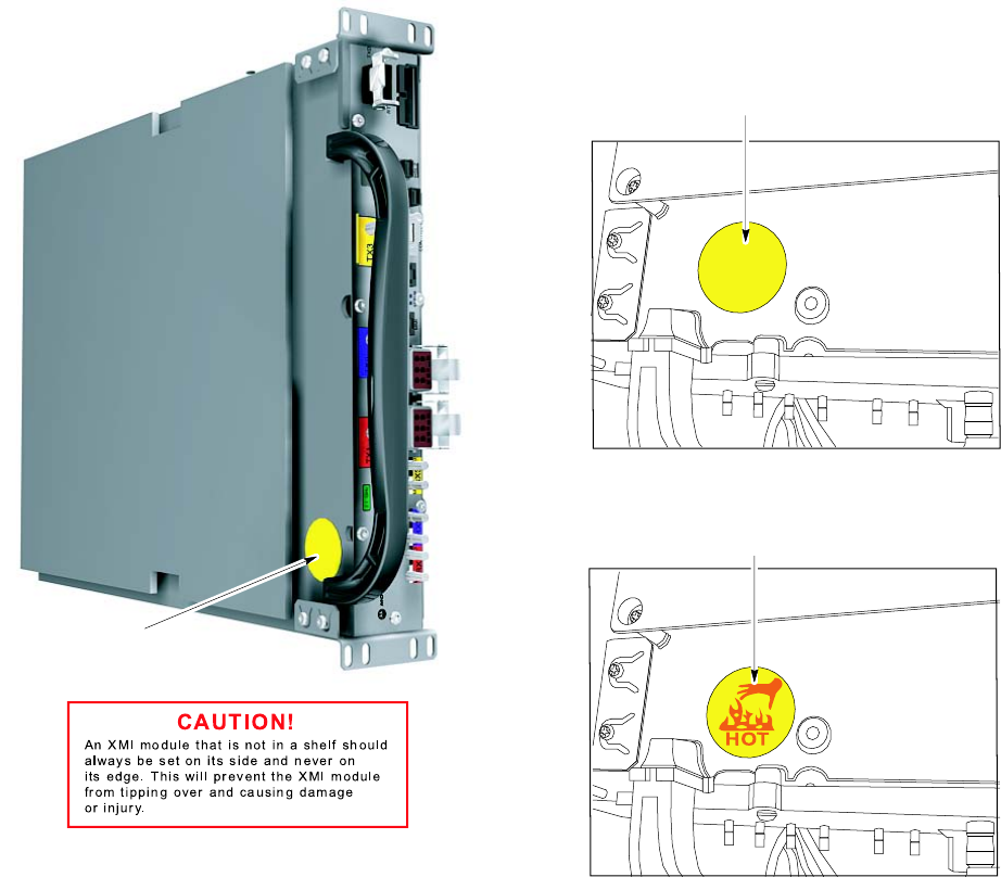
XMI “HOT" Warning Label Details
The XMI has a “HOT" warning label attached to it (see Figure 7 -1 for label location and
indications).
The hot warning label senses the surface temperature of the metal XMI housing. When the
XMI surface temperature reaches 50 degrees C , the “HOT" warning is fully visible indicating
that the XMI is too hot to touch and may cause burns. The “HOT" warning is partially visible
at temperatures that are slightly lower than 50 degrees C . When the “HOT" warning is not
visible at all, the XMI is safe to touch.
Figure 7 -1 XMI “HO T” W arning Label Details
ti-cdma-05889.eps
HOT
XMI Not Hot
Indication
XMI Hot Warning Label Close–ups
(XMI View Rotated 90 Degrees Clockwise)
XMI HOT
Indication
XMI
XMI Hot Warning Label Location
(See Label Close–ups)
CAUTION!
An XMI m o d u le th a t is n o t in a s he lf s h o u ld
a lwa ys b e s e t o n its s id e a n d n e ve r o n
its e d g e . Th is will p re ve n t th e XMI m o du le
fro m tip p ing o ve r a n d c a u s ing d a m a g e
o r in ju ry.
(Top-to-Bottom Positioning Shown Here
Is Same As When Installed In Frame)
7 -12 68P09283A64 -3
FOA SEP 2007

1X UBS Macro B T S FRU XMI (T r ansceiv er Module Internal) Module
Prerequisites
Do not touch the XMI with unprotected hands when the “HO T" label is fully visible. If
the “HO T" label is fully visible, wear heat protectiv e glo v es when touching the metal
case of the XMI. The “HO T" label becomes fully visible when the temper ature of the
metal case of the XMI reaches 50 degrees C. Howev er , the label ma y be partially
visible at lower case temper atures.
The XMI module is hea vy . T wo people are required to lift, carry , or handle the XMI
module.
•Be sure the remo v able XMI handle is attached to the front of the XMI before
ph ysically handling the module.
•Be sure two people use both hands and wear protectiv e footwear when handling
the XMI.
•Be sure to use two people to support the module while sliding the module out of
or into the shelf slot.
An XMI module that is not in a shelf should alw a ys be set on its side and nev er on
its edge. This will prev ent the XMI module from tipping o v er and causing damage
or injury .
This procedure requires working on or around circuitry extremely sensitiv e to ESD .
W ear a conductiv e, high impedance wrist str ap during the procedure.
F ollow appropriate safet y measures.
The XMI should be lock ed b y the OMCR oper ator just prior to being remo v ed.
68P09283A64 -3 7 -13
FOA SEP 2007

XMI (T r ansceiv er Module Internal) Module Chapter 7: XMI R eplacement Procedures
Coordinate this repair task with the OMCR operator .
Before You Begin
Before you begin, record the pertinent information in the following table (see T able 7 -3 ):
Table 7 -3 Item Number R eplacement List
Item
Number
BTS number
XMI number
XMI Replacement Procedures
The XMI replacement procedures consist of removing the failed XMI and then installing the
replacement XMI.
XMI Removal
F ollow the steps in Procedure 7 -1 to remove the XMI.
Procedure 7 -1 XMI R emo v al Procedure
A T THE BTS SITE
1
Notify the OMC-R operator that you are replacing the XMI.
A T THE OMCR
2
Open a CLI window . Refer to Accessing OMCR CLI window on page 3- 3 .
3
It will be helpful if the OMC-R operator executes “ENABLE EVENTS" command at the CLI
session of the OMC-R to monitor alarms. This command is optional and may not be useful if
executed during a high CP U utilization time.
4
Display the overall status of all devices at the BTS , including
the XMI, by entering the following command at the prompt:omc-00000> DISPLAY BTS-<bts#> STATUS
5
Determine the status of XMI 1 by observing the BTS ST A TUS report.
•F or a failed XMI 1 that is in an out-of -service (OOS) state, go to step 8 .
•F or a failed XMI 1 that is in an in service (INS) state, go to step 6 .
Continued
7 -14 68P09283A64 -3
FOA SEP 2007
1X UBS Macro B T S FRU XMI (T r ansceiv er Module Internal) Module
Procedure 7 -1 XMI R emo v al Procedure (Continued)
6
Lock the failed XMI by entering the following command at the prompt:omc-000000> LOCK XMI-<bts#>-<xmi#> UNC
7
Display the status of the XMI, by entering the following command at the prompt:omc-000000> DISPLAY BTS-<bts#> STATUS
V erify that the failed XMI is in an OOS_MANU AL state. Go to step 8 .
A T THE BTS SITE
8
Shut down DC power to the failed XMI by setting the corresponding XMI PDU DC circuit
breaker to OFF (pulled out).
Do not touch the XMI with unprotected hands when the “HO T" label is fully visible.
If the “HO T" label is fully visible, wear heat protectiv e glo v es when touching the
metal case of the XMI. The “HO T" label becomes fully visible when the temper ature
of the metal case of the XMI reaches 50 degrees C. Howev er , the label ma y be
partially visible at lower case temper atures.
W ear a conductiv e high impedance ESD wrist str ap while performing the steps
of this procedure.
9
F or cables, disconnect the cable b y pulling the connector - NOT b y pulling on the
cable.
If necessary , label the cables before disconnecting them to
ensure there is no uncertainty when reconnecting them.
Disconnect all cables from the XMI front panel and move them out of the
way .
10
F or 800 MHz XMI only , remove the TXD attenuator from the TXD connector on the XMI front
panel. This TXD attenuator will be reinstalled on the replacement XMI.
Continued
68P09283A64 -3 7 -15
FOA SEP 2007
XMI (T r ansceiv er Module Internal) Module Chapter 7: XMI R eplacement Procedures
Procedure 7 -1 XMI R emo v al Procedure (Continued)
11
A ttach the removable XMI handle to the front of the failed XMI module (see Figure 1-9
800 MHz XMI Module Front P anel I/O Detail on page 1- 38 or Figure 1-10 1.9 GHz XMI
Module Front P anel I/O Detail on page 1- 39 for location of XMI handle mounting screw
holes) as follows:
•Align handle screw holes with handle mounting screw holes on the XMI front panel.
(Note handle orientation; handle is not symmetrical.)
•Insert two M5 screws.
•Using a T25 TORX driver , tighten the screws to 3.2-3.6 N-m (28-32 in-lb).
12
Using a T25 TORX driver , remove the four XMI mounting screws; two screws at each of the
top and bottom mounting tabs on the front of the module.
13
The XMI module is hea vy . T wo people are required to lift, carry , or handle the
XMI module.
•Be sure the remo v able XMI handle is attached to the front of the XMI before
ph ysically handling the module.
•Be sure two people use both hands and wear protectiv e footwear when
handling the XMI.
•Be sure to use two people to support the module while sliding the module
out of or into the shelf slot.
An XMI module that is not in a shelf should alw a ys be set on its side and nev er on
its edge. This will prev ent the XMI module from tipping o v er and causing damage
or injury .
This step requires two people. P erform the following:
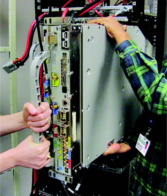
•(See Figure 7-2 T wo P eople Properly Removing/Installing an XMI (removable XMI handle
attached) on page 7- 17 .) One person grasp the XMI by the handle with both hands and
pull outward sliding the module out of the shelf slot. The second person supports the
bottom of the module with one hand and the top of the module with the other hand.
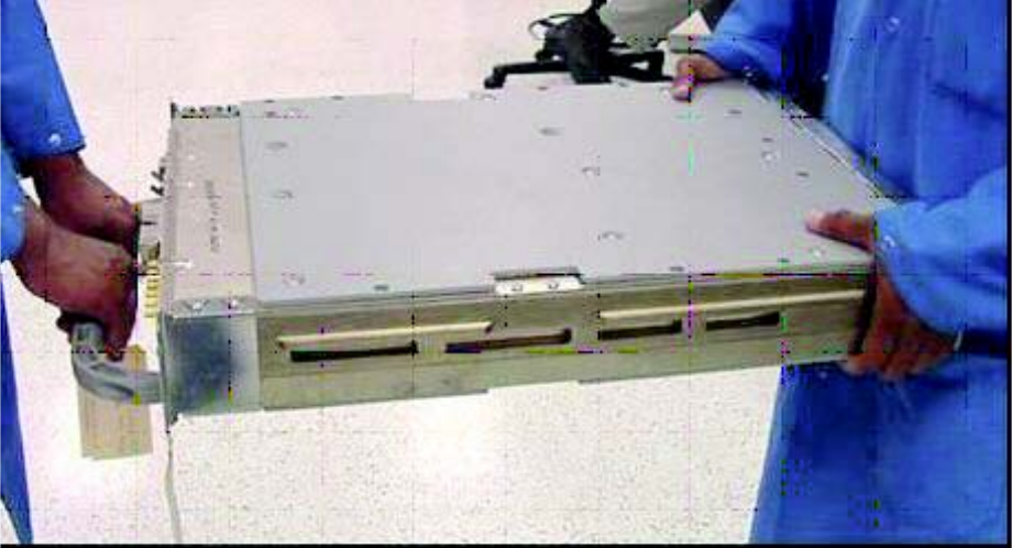
•(See Figure 7-3 T wo P eople Properly Carrying an XMI (removable XMI handle attached)
on page 7- 18 .) Carry the XMI module away from the frame and set it down on its side
not on its edge.
7 -16 68P09283A64 -3
FOA SEP 2007
1X UBS Macro B T S FRU XMI (T r ansceiv er Module Internal) Module
Figure 7 -2 T wo P eople Properly R emo ving/Installing an XMI (remo v able XMI handle
attached)
ti-cdma-06375.eps
68P09283A64 -3 7 -17
FOA SEP 2007
XMI (T r ansceiv er Module Internal) Module Chapter 7: XMI R eplacement Procedures
Figure 7 -3 T wo P eople Properly Carrying an XMI (remo v able XMI handle attached)
ti-cdma-05891.eps
7 -18 68P09283A64 -3
FOA SEP 2007
1X UBS Macro B T S FRU XMI (T r ansceiv er Module Internal) Module
XMI Installation Procedure
F ollow the steps in Procedure 7 -2 to install the XMI.
Procedure 7 -2 XMI Installation Procedure
A T THE BTS SITE
The XMI module is hea vy . T wo people are required to lift, carry , or handle the
XMI module.
•Be sure the remo v able XMI handle is attached to the front of the XMI before
ph ysically handling the module.
•Be sure two people use both hands and wear protectiv e footwear when
handling the XMI.
•Be sure to use two people to support the module while sliding the module
out of or into the shelf slot.
An XMI module that is not in a shelf should alw a ys be set on its side and nev er on
its edge. This will prev ent the XMI module from tipping o v er and causing damage
or injury .
1
The replacement XMI module should already have the removal handle attached.
If handle
is not
attached, go to step 2 .
If handle is attached, go to step 3 .
2
A ttach the removable XMI handle to the front of the replacement XMI module (see Figure 1-9
800 MHz XMI Module Front P anel I/O Detail on page 1- 38 or Figure 1-10 1.9 GHz XMI
Module Front P anel I/O Detail on page 1- 39 for location of XMI handle mounting screw
holes) as follows:
•Align handle screw holes with handle mounting screw holes on the XMI front panel.
(Note handle orientation; handle is not symmetrical.)
•Insert two M5 screws.
•Using a T25 TORX driver , tighten the screws to 3.2-3.6 N-m (28-32 in-lb).
Continued
68P09283A64 -3 7 -19
FOA SEP 2007

XMI (T r ansceiv er Module Internal) Module Chapter 7: XMI R eplacement Procedures
Procedure 7 -2 XMI Installation Procedure (Continued)
3
This step requires two people. P erform the following:
•(See Figure 7-3 T wo P eople Properly Carrying an XMI (removable XMI handle attached)
on page 7- 18 .) One person grasp the XMI by the handle with both hands. The second
person grasp the XMI fan tray sides with both hands. Using safe lifting technique (i.e.
lift with your legs not your back), Use legs to lift (Do not use your back) pick up the XMI
and carry it over to the front of the frame.
•(See Figure 7-2 T wo P eople Properly Removing/Installing an XMI (removable XMI
handle attached) on page 7- 17 .) While one person holds the XMI by the handle with
both hands, the second person supports the bottom of the module with one hand and the
top of the module with the other hand. Lift the XMI into the appropriate slot rails and
gently slide it all of the way into the shelf slot.
4
Insert the four XMI mounting screws; two screws at each of the top and bottom mounting tabs
on the front of the module. Using a T25 TORX driver , tighten the screws to 4.77 N-m (42 in-lb).
5
If desired, remove the handle from the front of the replacement XMI module as follows:
•Using a T25 TORX driver , remove the two screws that secure the handle to the XMI
front panel.
•Retain the two screws with the XMI handle for future use.
6
F or 800 MHz XMI only , install the TXD attenuator , previously removed from the failed XMI,
into the TXD connector on the front panel of the replacement XMI.
7
Reconnect all cables to the XMI front panel.
8
Restore power to the XMI by setting the corresponding XMI PDU DC circuit breaker to
ON (pushed in).
9
This completes the physical installation of the FRU . If optimization is to be performed at this
time, see Optimization Recommended following this table.
A T THE OMCR
10
Open a CLI window . Refer to Accessing OMCR CLI window on page 3- 3 .
11
Display the overall status of all devices at the BTS , including
the XMI, by entering the following command at the prompt:omc-000000> DISPLAY BTS-<bts#> STATUS
12
Determine the status of XMI 1 by observing the BTS ST A TUS report.
13
Unlock the replacement XMI by entering the following command at the prompt:omc-000000> UNLOCK XMI-<bts#>-<xmi#> UNC
14
Display the status of the XMI by entering the following command at the prompt:omc-000000> DISPLAY BTS-<bts#> STATUS
V erify that the replacement XMI is in an INS_ACTIVE state.
15
From the OMCR, monitor the Alarm Manager . V erify that old alarms are cleared and no
new alarms are reported.
7 -20 68P09283A64 -3
FOA SEP 2007
1X UBS Macro B T S FRU XMI (T r ansceiv er Module Internal) Module
Optimization Recommended
P erform the following BTS Optimization/A TP procedures:
•BTS Device Database Audit
•BTS Device Database Update
•TX P ath Calibration Audit
•Spectral Purity TX Mask A TP (optional)
•W aveform Quality (Rho) A TP (optional)
•Code Domain P ower A TP (optional)
•RS SI T est (FER T est is optional)
Refer to the
1X UBS Macro BTS Optimization/A TP
manual for the optimization procedures.
68P09283A64 -3 7 -21
FOA SEP 2007

XMI F an T r a y Assembly Chapter 7: XMI R eplacement Procedures
XMI Fan Tray Assembly■■■■■■■■■■■■■■■■■■■■■■■■■■■■■■■■■■■■■■■■■■■■■■■■■■■■■■■■■■■■■■
■
■
XMI Fan Tray Assembly Description
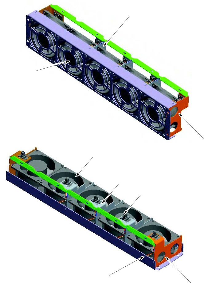
The XMI fan tray assembly consists of five 27 V DC fans mounted in a housing. This housing is
the removable rear panel of the XMI. (See Figure 7 -4 and Figure 7 -5 .)
The fan tray assembly mounted on the rear of the XMI draws cooling air in from air vents on the
XMI front panel through the XMI and exhausts air out the XMI rear panel.
The XMI fan housing contains five fan mounting locations. Each fan mounting location has the
following:
•built -in fan grille/finger -guard
•four vibration isolator fan mounting posts
•fan connector bracket
Each individual fan has a electrical wiring and connector . The connector mounts in the
corresponding fan connector bracket.
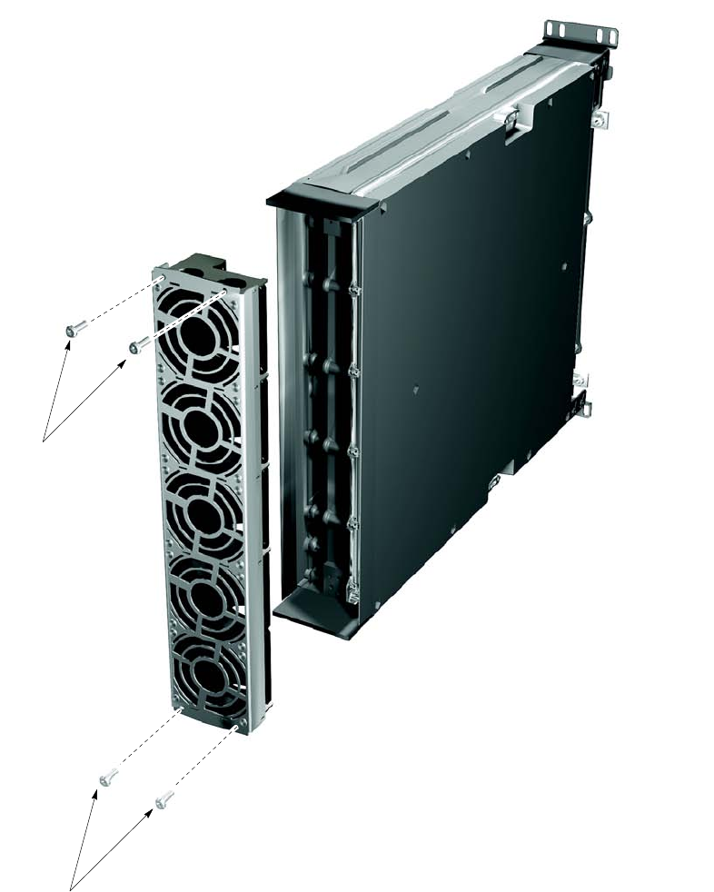
The XMI fan tray assembly is attached to the rear of the XMI and secured with four screws.
When the XMI fan tray assembly is attached to the rear of the XMI, the five fan connectors mate
with connectors on the XMI F an Interconnect Board (FIB).
The XMI FIB provides a DC voltage connection to each fan in the fan tray assembly and is a
conduit for fan speed information and control.
The XMI P A Controller (XP AC) provides central control of the three LP A sections. In addition,
the XP AC gathers LP A alarms and provides XMI fan speed control.
System Impact/Considerations
Typically the XMI fan tray assembly replacement requires that the affected XMI be physically
removed from the UBS Macro BTS frame. However , if the rear of the frame is accessible, the XMI
fan tray assembly can be replaced without physically removing the affected XMI from the frame.
P erforming this replacement procedure on a frame with only one XMI will cause BTS
downtime and suspend call processing.
If the frame is equipped with only one XMI, BTS service will be interrupted during the XMI fan
tray assembly replacement. If the frame is equipped with more than one XMI, only the affected
XMI will be out -of -service and the BTS will remain in service.
Alarms will be reported during the replacement procedure.
7 -22 68P09283A64 -3
FOA SEP 2007

1X UBS Macro B T S FRU XMI F an T r a y Assembly
Table 7 -4 FRU R eplacement Conditions
FRU
What to Shut Down...
XMI fan tray assembly From the OMCR, lock the XMI being removed. Then shut
down XMI DC input power .
XMI Fan Tray Diagrams
Figure 7 -4 shows how the fan tray assembly is attached to the rear of the XMI.
Figure 7 -5 shows the fan tray assembly with five fans, built -in fan grille/finger -guards and five
fan connector brackets with individual fan connectors and wiring.
68P09283A64 -3 7 -23
FOA SEP 2007
XMI F an T r a y Assembly Chapter 7: XMI R eplacement Procedures
Figure 7 -4 XMI F an T r a y Assembly (R emo v al & Installation)
ti-cdma-05918.eps
XMI (Rear View)
XMI Fan Tray
Assembly
Mounting Screws
(T20 Head)
Mounting Screws
T20 Head)
7 -24 68P09283A64 -3
FOA SEP 2007
1X UBS Macro B T S FRU XMI F an T r a y Assembly
Figure 7 -5 XMI F an T r a y Assembly (External & Internal Views)
ti-cdma-05919.eps
Fan Connector
Bracket (5)
Fan Grille/Finger-Guard
XMI Fan
Housing
Internal View
Fan
Fan Connector
Bracket (5)
Fan Connector
Fan Wiring XMI Fan
Housing
68P09283A64 -3 7 -25
FOA SEP 2007

XMI F an T r a y Assembly Chapter 7: XMI R eplacement Procedures
Required Items
Manpower
•T wo people are required to lift, carry , or handle the XMI module.
Documents
•None
Tools
•T20 TORX Bit
•T25 TORX Bit
•T orque Driver
•XMI removable handle with two M5 screws
•Heat protective gloves for handling/touching a “HOT" XMI
Replacement Unit
•XMI fan tray assembly with five 27 V DC fans (Motorola model STLN6404)
Prerequisites
Do not touch the XMI with unprotected hands when the “HO T" label is fully visible. If
the “HO T" label is fully visible, wear heat protectiv e glo v es when touching the metal
case of the XMI. The “HO T" label becomes fully visible when the temper ature of the
metal case of the XMI reaches 50 degrees C. Howev er , the label ma y be partially
visible at lower case temper atures.
XMI fans must be completely stopped before remo ving the XMI fan tr a y assembly .
7 -26 68P09283A64 -3
FOA SEP 2007
1X UBS Macro B T S FRU XMI F an T r a y Assembly
The XMI should be lock ed b y the OMCR oper ator just prior to remo ving the XMI or the
XMI fan tr a y assembly .
Coordinate this repair task with the OMCR operator .
Before You Begin
Before you begin, record the pertinent information in the following table (see T able 7 -5 ):
Table 7 -5 Item Number R eplacement List
Item
Number
BTS number
XMI number
XMI Fan Tray Assembly Replacement
F ollow the steps in Procedure 7 -3 to replace an XMI fan tray assembly .
Procedure 7 -3 XMI F an T r a y Assembly R eplacement Procedure
A T THE BTS SITE
1
Notify the OMC-R operator that you are replacing the XMI fan tray assembly .
Do not touch the XMI with unprotected hands when the “HO T" label is fully visible.
If the “HO T" label is fully visible, wear heat protectiv e glo v es when touching the
metal case of the XMI. The “HO T" label becomes fully visible when the temper ature
of the metal case of the XMI reaches 50 degrees C. Howev er , the label ma y be
partially visible at lower case temper atures.
2
If the affected XMI is going to be removed from the frame in order to replace the
XMI fan tray assembly , go to Procedure 7-1 XMI Removal Procedure on page 7- 14
and perform the steps starting at step 2 . Then return to step 3 of this procedure.
If the affected XMI is going to be accessed from the rear of the frame in order to replace
Continued
68P09283A64 -3 7 -27
FOA SEP 2007
XMI F an T r a y Assembly Chapter 7: XMI R eplacement Procedures
Procedure 7 -3 XMI F an T r a y Assembly R eplacement Procedure (Continued)
the XMI fan tray assembly , go to Procedure 7-1 XMI Removal Procedure on page 7- 14 and
perform the steps starting at step 2 , but stop after step step 8 . Then return to step step 3 of
this procedure.
XMI fans must be completely stopped before remo ving the XMI fan tr a y assembly .
3
W orking at the rear of the affected XMI, make sure that all five of the XMI fans have
completely stopped.
4
Using a T20 TORX driver , remove the four XMI fan tray assembly mounting screws (see
Figure 7-4 for screw locations.)
5
Grasp the XMI fan tray assembly and firmly pull it away from the rear of the XMI.
6
Properly position the replacement XMI fan tray assembly at the rear of the XMI. Make sure
that all five fan connectors are properly aligned with the mating connectors on the XMI.
7
Firmly push the XMI fan tray assembly onto the rear of the XMI. Make sure that all five fan
connectors are fully seated.
8
Insert the four XMI fan tray assembly mounting screws. Using a T20 TORX driver , tighten
the screws to 1.6 - 1.8 N-m (14 - 16 in-lb).
9
If the affected XMI is removed from the frame, go to Procedure 7-2 XMI
Installation Procedure on page 7- 19 and perform the steps starting at step 3 .
If the affected XMI is being accessed from the rear of the frame, go to Procedure 7-2 XMI
Installation Procedure on page 7- 19 and perform the steps starting at step 8 .
There is no optimization required for XMI fan tray assembly replacement.
7 -28 68P09283A64 -3
FOA SEP 2007

C h a p t e r
8
DMI Replacement Procedures■■■■■■■■■■■■■■■■■■■■■■■■■■■■■■■■■■■■■■■■■■■■■■■■■■■■■■■■■■■■■■
■
■
■
■
68P09283A64 -3 8 -1
SEP 2007 FOA

DMI R eplacement Procedures Chapter 8: DMI R eplacement Procedures
DMI Replacement Procedures■■■■■■■■■■■■■■■■■■■■■■■■■■■■■■■■■■■■■■■■■■■■■■■■■■■■■■■■■■■■■■
■
■
Introduction
This chapter includes FRU replacement procedures for the following:
•DMI (Digital Module Internal) Assembly – This section covers the following:
Preparing the replacement DMI assembly in the Field.
Replacing the DMI.
Dismantling the failed DMI assembly in the Field.
and more
•Modem Boards – This section covers the replacement of a failed 1X CDMA or EV -DO
modem board in a UBS Macro BTS DMI.
8 -2 68P09283A64 -3
FOA SEP 2007

1X UBS Macro B T S FRU DMI (Digital Module Internal) Assembly
DMI (Digital Module Internal) Assembly■■■■■■■■■■■■■■■■■■■■■■■■■■■■■■■■■■■■■■■■■■■■■■■■■■■■■■■■■■■■■■
■
■
The R20 UBS Macro BTS only supports frame configurations with up to two DMIs
and up to two XMIs.
DMI Description
The UBS Macro BTS frame must be equipped with at least one instance of the DMI. A second
DMI is optional. The DMIs are located in the right side of the XMI shelf in the UBS Macro BTS
frame (see Figure 1 -1 UBS Macro BTS low -tier/low -capacity frame (1000 mm rack) on page
1 - 27 ,Figure 1 -2 Low capacity UBS Macro BTS starter frame (1800 mm rack) on page 1 - 28 and
Figure 1 -3 UBS Macro BTS mid -capacity frame (1800 mm rack) on page 1 - 30 ). The DMIs are
stacked vertically in an XMI shelf slot. DMI 1 is on the top and DMI 2 is on bottom. If the
optional second DMI is not equipped, an empty DMI outer housing is in the DMI 2 position.
The DMI includes a DMI assembly that slides into a DMI outer housing. The DMI assembly
consists of a chassis with a controller board, two rear mounted cooling fans and a front panel.
The DMI assembly may also be equipped with up to two modem boards. When the UBS Macro
BTS frame equipment is shipped from the factory the DMI assembly is equipped with at least one
modem board. A second modem board is optional and may be either factory or field installed.
The DMI can be equipped with either 1X CDMA modem boards, EV -DO modem boards, or a
combination of one 1X CDMA modem board and one EV -DO modem board.
Each modem board mounts on opposite sides of the controller board. Modem board -to -controller
board electrical connection is via a printed circuit board mounted High Density Mezzanine
(HDMEZZ) type connector . Each modem board is secured to the DMI assembly chassis with
seven screws that are captivated to the modem board.
Figure 8 -1 Removing and installing Modem 1 on page 8 - 13 and Figure 8 -2 Removing and
installing Modem 2 on page 8 - 14 show the locations of Modem 1 and Modem 2 within the
DMI assembly .
The following rules apply to modem board location within the DMI:
•F or a DMI equipped with one 1X CDMA modem board, the 1X CDMA modem
board is always Modem 1 location
•F or a DMI equipped with one EV -DO modem board, the EV -DO modem board
is always Modem 2 location
•F or a DMI equipped with a combination of one 1X CDMA modem board and one
EV -DO modem board, the 1X CDMA modem board is always Modem 1 location
and the EV -DO modem board is always Modem 2 location
68P09283A64 -3 8 -3
FOA SEP 2007

DMI (Digital Module Internal) Assembly Chapter 8: DMI R eplacement Procedures
The DMI assembly is the FRU (i.e., spare) that is used for DMI replacement. This assembly
includes a chassis with a controller board, fans, front panel and two modem boards. This
assembly does not include an outer housing. The DMI outer housing in the UBS Macro BTS
frame is reused.
The DMI FRU that is used for DMI replacement can be either of the following:
•F actory built DMI assembly – consisting of a DMI chassis, controller board, fans, front
panel and two modem boards (i.e., 1X CDMA, EV -DO , or a combination of both).
•Field prepared DMI assembly – consisting of a DMI chassis, controller board, fans, front
panel and up to two modem boards (i.e., 1X CDMA, EV -DO , or a combination of both)
that are added to the assembly in the field.
This chapter provides a procedure describing how to field prepare a DMI assembly , by
installing up to two modems, so that it matches the configuration of the failed DMI.
The DMI assemblies do not include an outer housing. The DMI outer housing in the UBS Macro
BTS frame is reused.
The typical DMI replacement scenario is as follows:
1. Remove the failed DMI assembly from its outer housing in the UBS Macro BTS frame.
2. Remove the replacement DMI assembly from its packaging and install it into the outer
housing in the UBS Macro BTS frame.
3. Place the failed DMI assembly into the packaging that the replacement DMI came in.
The DMI assembly FRU is used as a replacement for a DMI with an internal DMI
component failure (including controller board, modem board, fan, or front panel
failure). Although, a DMI with a modem board failure can just have the failed modem
board replaced. This is covered in the Modem Board section of this chapter .
This chapter also provides a procedure describing how to dismantle a failed DMI
assembly in the field. This procedure is used if it is desired to reclaim known good
FRUs from the failed DMI assembly . A fter dismantling the DMI assembly , the failed
portion may be returned to Motorola for repair and the reclaimed known good FRUs
may be restocked.
8 -4 68P09283A64 -3
FOA SEP 2007

1X UBS Macro B T S FRU DMI (Digital Module Internal) Assembly
System impact/considerations
If the UBS Macro BTS frame is equipped with one DMI, then performing this
replacement procedure will cause BTS downtime and suspend all call processing .
If the UBS Macro BTS frame is equipped with two DMIs, then performing this
replacement procedure for the Site Master DMI will temporarily cause BTS downtime.
This is due to soft reset of the non -Site Master DMI during the DMI swap procedure.
As soon as the DMI swap procedure is finished, the non -Site Master DMI becomes
the Site Master DMI and call processing resources are available, but temporarily
reduced until the failed DMI is replaced.
P erforming this replacement procedure for a non -Site Master DMI will not cause
BTS downtime, but call processing resources will be temporarily reduced until the
failed DMI is replaced.
Call traffic processing through the site will be temporarily interrupted by the DMI replacement
procedure.
Alarms will be generated during the DMI replacement procedure.
The DMI is not hot swappable.
DMI removal requires shutting down DC power to the DMI as well as disconnection of all
DMI cables.
Table 8 -1 DMI R eplacement Conditions
FRU
Ref Designator What to Shutdown...
Digital Module
Internal
DMI
From the OMCR, lock the DMI being removed.
Then shut down the DMI DC input power .
Required items
Documents
•
1X UBS Macro BTS Optimization/A TP
manual.
68P09283A64 -3 8 -5
FOA SEP 2007

DMI (Digital Module Internal) Assembly Chapter 8: DMI R eplacement Procedures
Tools
•T20 TORX bit.
•T orque driver .
•ESD wrist straps.
•ESD floor and bench top mats.
•ESD containers.
Replacement Units
All models of DMI assemblies include: DMI chassis with controller board, fans and
front panel.
F actory built DMI assemblies:
•DMI assembly with one 1X CDMA modem board (Motorola model STLN6681).
•DMI assembly with one EV -DO modem board (Motorola model STLN6682).
•DMI assembly with two 1X CDMA modem boards (Motorola model STLN6683).
•DMI assembly with one 1X CDMA modem board and one EV -DO modem board (Motorola
model STLN6684).
•DMI assembly with two EV -DO modem boards (Motorola model STLN6679).
— OR —
Field prepared DMI assembly consisting of:
•DMI assembly without modem boards (Motorola model STLN6325). Up to two modem
boards are added to the assembly in the field. Add the appropriate quantities of the
following:
CDMA 1X Modem Board (Motorola model SGLN6336).
— AND/OR —
EV -DO Modem Board (Motorola model SGLN6494).
8 -6 68P09283A64 -3
FOA SEP 2007

1X UBS Macro B T S FRU DMI (Digital Module Internal) Assembly
DMI I/O Panel Connectors/Ports & LEDs
DMI I/O Panel
Figure 1 -11 DMI Module Front P anel Detail on page 1 - 41 shows I/O connectors on the front
panel of the UBS Macro BTS DMI. The top -to -bottom positioning of the DMI shown in the figure
is the same as when it is installed in the rack. This figure shows connector/port locations,
connector types and brief cabling details.
DMI Connectors/Ports
The following text describes each connector/port on the DMI front panel.
•+27VDC - DMI DC input power connections. Connects to corresponding DMI DC power
connector on the PDU of the UBS Macro BTS frame. The PDU DMI DC power connector
supplies protected +27 V via a 20 A circuit breaker .
•IDI/S SI 1 and S SI 2 - Serial backhaul traffic and control data connectors provide serial
data links between the DMI and the corresponding S SIs. The S SI 2 port is currently not
used.
The R20 UBS Macro BTS does not support frame configurations with an IDI
(Interworking DMI Interconnect) application.
•XMI 1/BSI and XMI 2 - High -speed Serial data Link (HSL) port connectors that each
provide a 1.2288 Gbps high -speed serial data links between the DMI and the respective
XMI. The high -speed serial data links support the transfer of baseband I & Q data as well
as control data between the DMI and XMI. These connectors are cabled to the appropriate
HSL 1 or HSL 2 high -speed serial data link connector on the XMI front I/O panel.
The R20 UBS Macro BTS does not support frame configurations with a BSI
(Baseband Switch Interface) application.
The MMI and LMT ports are intended to be used primarily for testing or debugging
purposes b y Motorola. These ports ma y be used in the eld for maintenance purposes
b y customers. Carefully follow written procedures when using these ports in the eld.
F ailure to do so could result in an inoper able FRU .
68P09283A64 -3 8 -7
FOA SEP 2007

DMI (Digital Module Internal) Assembly Chapter 8: DMI R eplacement Procedures
•RS232 -1 and RS232 -2 - Debug RS -232 ports allow MMI access to the DMI controller
board via a computer terminal through either a modem or a null modem cable. These MMI
ports are 8 -pin RJ -45 connectors.
•LMT and TEST - These ports are intended for development use only . These debug ports
are configured for full -duplex fast Ethernet 10/100BaseT and allows local MMI access
to the DMI controller board via a Local Maintenance T erminal (LMT) with an Ethernet
interface. The LMT and TEST ports are 8 -pin RJ -45 connectors.
DMI LEDs
T able 8 -2 shows the possible states for the DMI front panel LEDs and the corresponding
indications. These LED indicators are located on the DMI front panel next to the DMI +27 V
DC connector (see Figure 1 -11 DMI Module Front P anel Detail on page 1 - 41 ) and are labeled
as follows:
•ALM (ALARM)
•INST (INST ANCE)
•ST (ST A TUS)
Table 8 -2 DMI LEDs States and Indications
ALM (Red) LED State INST LED State
ST A (Green) LED
State
Indication
Off Off Off
No DC P ower to FRU
On Orange On
LED Indicator T est (temporary; 0.5 sec
to 1 sec)
On
N/A
Off FRU F ailure
Off
N/A N/A
No FRU F ailure
Flashing
(1.5 sec-On/1
sec-Off)
N/A N/A
P artial (soft) FRU F ailure
N/A N/A
Flashing
(250 ms-On/250
ms-Off)
FRU Booting up (not active)
N/A N/A
On FRU Active
N/A
Green Flashing
(0.5 sec-On/0.5
sec-Off cycle count)
followed by 3
sec-Off
N/A
Instance Indicator and No FRU
Cabling Connection Errors Detected.
Cycle count equals FRU type instance;
where: 1 flash = 1st instance, 2 flashes
= 2nd instance, 3 flashes = 3rd instance,
so on and so forth.
N/A
Red
N/A
FRU Cabling Connection Error Detected
N/A = LED state is Not Applicable to indication
8 -8 68P09283A64 -3
FOA SEP 2007
1X UBS Macro B T S FRU DMI (Digital Module Internal) Assembly
Prerequisites
ESD handling precautions must be adhered to when handling and working on the DMI
assembly or the modem boards. W ear a conductiv e, high impedance wrist str ap
during handling. All work performed on the DMI assembly and modem boards must
be done in an ESD protected work area.
The procedures in this chapter requires working on or around circuitry that is extremely
sensitive to ESD .
Coordinate the DMI replacement task with the OMCR operator .
Before You Begin
Before you begin, record the pertinent information in the following table (see T able 8 -3 ):
Table 8 -3 Item Number R eplacement List
Item Number
BTS number
DMI number
If the failed DMI is to be replaced with a “field prepared DMI assembly”, it will be necessary
to have a work area that meets the criteria described in DMI Preparation Area on page 8 - 10 .
Then it will be necessary to prepare the complete DMI assembly by performing Procedure 8 -1
Preparing the replacement DMI assembly in the Field on page 8 - 11 prior to performing the
Procedure 8 -2 Replacing the DMI on page 8 - 15 .
68P09283A64 -3 8 -9
FOA SEP 2007

DMI (Digital Module Internal) Assembly Chapter 8: DMI R eplacement Procedures
DMI Preparation Area
The DMI preparation area should provide the following ESD protection and the proper
environmental conditions.
•ESD Protection:
Always wear a ground strap which must be connected to the electrostatic point on
the equipment.
Leave any conductive foam pieces on connectors or leads until the last moment.
Remove these pieces just before installing the device.
Do not wear outer clothing made of nylon or similar man made material. A cotton
overall is preferable.
If possible work on an grounded metal surface or anti -static mat. W ipe insulated
plastic work surfaces with an anti -static cloth before starting the operation.
All metal tools should be used and when not in use they should be placed on an
grounded surface.
T ake care when removing components connected to electrostatic sensitive devices.
These components may be providing protection to the device.
When mounted onto printed circuit boards (PCBs), MOS devices are normally less
susceptible to electrostatic damage. However PCBs should be handled with care,
preferably by their edges and not by their tracks and pins, they should be transferred
directly from their packing to the equipment (or the other way around) and never
left exposed on the workbench.
•Proper Environmental Conditions:
Preparation surface should be clean and dry .
Preparation environment should be clean and dry and provide protection such that
contaminates will not enter the equipment.
W ork environment should allow enough space and adequate lighting to accurately
align components during assembly .
DMI Field Preparation Procedure
P erform Procedure 8 -1 Preparing the replacement DMI assembly in the Field on page 8 - 11 in
the DMI preparation area. This procedure describes how to prepare a complete DMI assembly
from spares inventory that matches the failed DMI assembly . Up to two modems may be
installed into the DMI assembly . The following spares are required:
•DMI assembly without modem boards (Motorola model STLN6325) includes DMI chassis
with controller board, fans and front panel.
•CDMA 1X Modem Board (Motorola model SGLN6336); up to two modem boards as
required.
— AND/OR —
•EV -DO Modem Board (Motorola model SGLN6494); up to two modem boards as required.
8 -10 68P09283A64 -3
FOA SEP 2007
1X UBS Macro B T S FRU DMI (Digital Module Internal) Assembly
Procedure 8 -1 Preparing the replacement DMI assembly in the Field
A T THE OMCR
1
Ask the OMCR operator to get the EID information for the
failed DMI by entering the following command at the prompt:omc-000000> DISPLAY BTS-<bts#>- EID
Observe the displayed response. Record the model number of
the failed DMI and its modem board quantity and model numbers. Modem boards are
designated as HDMODEM. Check values for both HDMODEM numbers (i.e., 1, 2 for
DMI 1 and 21, 22 for DMI 2) on the affected DMI. If an HDMODEM number has a
blank value, then it does not exist.
IN THE DMI PREP ARA TION AREA
2
Based on the failed DMI EID information, determine the quantity and type of modem boards
needed to match that of the failed DMI.
3
Obtain the needed replacement units.
ESD handling precautions must be adhered to when handling and working on
the DMI assembly or the modem boards. W ear a conductiv e, high impedance
wrist str ap during handling. All work performed on the DMI assembly and modem
boards must be done in an ESD protected work area.
4
Remove the DMI assembly , without modems, from its shipping packaging. Set the DMI
assembly handle side up (see Figure 8-1 Removing and installing Modem 1 on page 8- 13 )
onto a clean, ESD protected surface. Retain the packaging for later reuse.
5
Remove the modem board(s) from its shipping packaging. Retain the packaging for later
reuse.
6
Install Modem 1 into the DMI assembly by performing the following:
1. Carefully place the front edge of Modem 1 under the lip of the DMI front panel.
2. Align the modem-to-controller connector halves so that they will mate together . In
order to ensure proper connector alignment prior to connector insertion, verify that
the modem screws are aligned with chassis mounted standoffs and that screws are
not at an angle.
3. Press down firmly on the black plastic modem connector handle until the connector
halves are fully seated. Approximately 70 N (15 lbs) of force is required to fully seat the
connector halves.
4. Using a T20 TORX bit and torque driver , tighten the seven captive screws that retain
Modem 1 to the replacement DMI assembly . Tighten the screws to 1.6 - 1.8 N-m (14 -
16 in-lb).
5. A fter tightening the screws, firmly squeeze the modem connectors together to make
sure that it is well seated. This may help prevent problems/errors that may not be
visible from the OMCR.
Continued
68P09283A64 -3 8 -11
FOA SEP 2007

DMI (Digital Module Internal) Assembly Chapter 8: DMI R eplacement Procedures
Procedure 8 -1 Preparing the replacement DMI assembly in the Field (Continued)
7
If the failed DMI assembly to be replace is equipped with Modem 2, go to step 8 otherwise
go to step 11 .
8
P osition the DMI assembly on its side with the front panel handle at the bottom (see
Figure 8-2 Removing and installing Modem 2 on page 8- 14 ).
9
Remove the modem board from its shipping packaging. Retain the packaging for later reuse.
10
Install Modem 2 from the failed DMI assembly into the replacement DMI assembly by
performing the following:
1. Carefully place the Modem 2 in the rear half of the DMI assembly .
2. Align the modem-to-controller connector halves so that they will mate together . In
order to ensure proper connector alignment prior to connector insertion, verify that
the modem screws are aligned with chassis mounted standoffs and that screws are
not at an angle.
3. Press down firmly on the black plastic modem connector handle until the connector
halves are fully seated. Approximately 70 N (15 lbs) of force is required to fully seat the
connector halves.
4. Using a T20 TORX bit and torque driver , tighten the seven captive screws that retain
Modem 2 to the replacement DMI assembly . Tighten the screws to 1.6 - 1.8 N-m (14 -
16 in-lb).
5. A fter tightening the screws, firmly squeeze the modem connectors together to make
sure that it is well seated. This may help prevent problems/errors that may not be
visible from the OMCR.
1 1
Place the field prepared DMI assembly , with modems, into the original packaging that the
DMI assembly was received in.
T o speed up code and data synchronization when this replacement DMI is placed
into the BTS (especially if it is the only DMI in the BTS), it is recommended to set
up a staging area for upgrading the code and base file for this replacement DMI to
the same version that is used at the site. A fterwards, the DMI may be packaged
and taken to the site.
12
T ake the field prepared DMI assembly , in it’s packaging, to the BTS site having the failed
DMI. P erform Procedure 8-2 Replacing the DMI on page 8- 15 .
Reference Diagrams
The following diagrams are used to aid the DMI replacement procedures.
8 -12 68P09283A64 -3
FOA SEP 2007
1X UBS Macro B T S FRU DMI (Digital Module Internal) Assembly
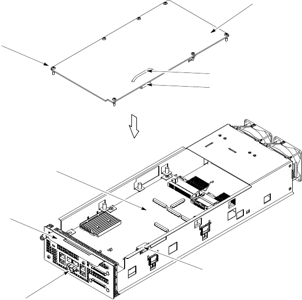
Figure 8 -1 shows the DMI assembly with its bottom side up for access to Modem 1.
Figure 8 -1 R emo ving and installing Modem 1
ti-cdma-06168.eps
7X
Captive Screws
Modem 1
Front Panel
HD MEZZ Connector
Modem Connector Handle
HD MEZZ Connector
Controller Board
Handle
68P09283A64 -3 8 -13
FOA SEP 2007

DMI (Digital Module Internal) Assembly Chapter 8: DMI R eplacement Procedures
Figure 8 -2 shows the DMI assembly with its top side up for access to Modem 2.
Figure 8 -2 R emo ving and installing Modem 2
ti-cdma-06169.eps
7X
Captive Screws
Modem 2
Front Panel
HD MEZZ Connector
Modem Connector Handle
HD MEZZ Connector
Controller Board
Handle
DMI Replacement Procedure
Procedure 8 -2 Replacing the DMI on page 8 - 15 includes:
1. Removing the failed DMI assembly from the UBS Macro BTS frame.
2. Removing the replacement DMI assembly from its packaging.
3. Installing the replacement DMI assembly , equipped with modems, into the UBS Macro
BTS frame.
8 -14 68P09283A64 -3
FOA SEP 2007

1X UBS Macro B T S FRU DMI (Digital Module Internal) Assembly
Procedure 8 -2 R eplacing the DMI
A T THE OMCR
1
If you have not already asked the OMCR operator to get
the EID information for the failed DMI, then have the
OMCR operator enter the following command at the prompt:omc-000000> DISPLAY BTS-<bts#>- EID
Observe the displayed response. Record the model number of
the failed DMI and its modem board quantity and model numbers. Modem boards are
designated as HDMODEM. Check values for both HDMODEM numbers (i.e., 1, 2 for
DMI 1 and 21, 22 for DMI 2) on the affected DMI. If an HDMODEM number has a
blank value, then it does not exist.
2
F or a UBS Macro BTS equipped with one DMI, go to step 3 .
F or a UBS Macro BTS equipped with more than one DMI, go to step 4 .
3
Shut down site signaling functions according to Procedure 3-2 Shutdown
site signaling functions procedure for a packet BTS on page 3- 5 .
A fter this step is completed, go to step 8 .
4
Determine if the failed DMI is the Site Master or not
by entering the following command at the prompt:omc-000000> STATUS DMI-<bts#>-<dmi#>- PHY
Observe the displayed response. SITECTRL=YES means the DMI is Site Master .
SITECTRL=NO means the DMI is not Site Master .
5
F or a failed DMI that
is
the Site Master , go to step 6 .
F or a failed DMI that
is not
the Site Master , go to step 7 .
6
Reset the failed DMI Site Master and force the other DMI to become
the Site Master by entering the following command at the prompt:omc-000000> RESET DMI-<bts#>-<dmi#>- UNC
7
Lock the failed DMI by entering the following command at the prompt:omc-000000> LOCK DMI-<bts#>-<dmi#>- UNC
A T THE BTS SITE
8
Based on the failed DMI EID information, determine the type of DMI that matches the
failed DMI.
9
Obtain the needed replacement DMI.
10
Set the replacement DMI assembly , in its packaging, near the UBS Macro BTS frame.
Continued
68P09283A64 -3 8 -15
FOA SEP 2007
DMI (Digital Module Internal) Assembly Chapter 8: DMI R eplacement Procedures
Procedure 8 -2 R eplacing the DMI (Continued)
1 1
P ower down the failed DMI by setting the corresponding PDU DMI 20A circuit breaker to
the off position (pulled out).
Mak e sure the PDU DMI circuit break er is set to OFF .
Y ou will be disconnecting multiple cables from connectors. If necessary , use
masking tape and a marker and temporarily tag each cable as to the proper
connector before disconnection.
12
ESD handling precautions must be adhered to during this procedure. W ear a
conductiv e, high impedance wrist str ap .
Plug the end of the ESD wrist strap into the UBS Macro BTS frame ESD jack This jack is
located in the middle of the upper XMI shelf bracket. A ttach the wrist strap to your wrist.
13
Disconnect all of the cables connected to the front panel connectors on the failed DMI.
14
Turn the retaining fastener , located in the upper right corner of the failed DMI front panel,
CCW (Counter Clockwise) until resistance is felt. This indicates that the retaining fastener
is disengaged.
15
Grasp the failed DMI by the handle with one hand and pull outward. While supporting the
bottom of the DMI assembly with the other hand, slide the failed DMI assembly completely
out of its housing.
16
ESD handling precautions must be adhered to when handling the DMI assembly .
Set the failed DMI assembly onto a clean, ESD protected surface.
17
Remove the replacement DMI assembly from its packaging.
Continued
8 -16 68P09283A64 -3
FOA SEP 2007

1X UBS Macro B T S FRU DMI (Digital Module Internal) Assembly
Procedure 8 -2 R eplacing the DMI (Continued)
18
Install the replacement DMI assembly , with modems, into the appropriate empty DMI
housing in the UBS Macro BTS frame by performing the following:
1. P osition the replacement DMI assembly on its bottom edge so that the front panel
handle is on the right and the retaining fastener is at the top.
2. Pick up the replacement DMI assembly with two hands.
3. Insert the rear of the replacement DMI assembly into the empty housing.
4. Slide the replacement DMI assembly completely into the housing.
5. Turn the retaining fastener CW (Clockwise) until finger tight to secure the DMI
assembly in the housing.
19
Place the failed DMI assembly , with modems, into the packaging that the replacement DMI
assembly came in.
20
Reconnect all of the cables to the corresponding connectors on the DMI front panel.
21
P ower up the DMI by setting the corresponding PDU DMI 20A circuit breaker to the on
position (pushed in).
A T THE OMCR
22
F or a UBS Macro BTS equipped with one DMI, go to step 23 .
F or a UBS Macro BTS equipped with more than one DMI, go to step 24 .
23
Restore site signaling operations according to Procedure 3-3 Restore
site signaling operations procedure for a packet BTS on page 3- 10 .
A fter this step is completed, go to step 25 .
24
Unlock the replacement DMI by entering the following command at the prompt:omc-000000> UNLOCK DMI-<bts#>-<dmi#>- UNC .
A T THE BTS SITE
25
P erform the recommended optimization and testing on the UBS Macro BTS frame (see
Optimization Recommended on page 8- 17 ).
26
Remove the failed DMI assembly , in its packaging, from the BTS site and do either of the
following:
•Transport it to the DMI Preparation Area for dismantling (see Dismantling the failed
DMI assembly in the Field on page 8- 18 ).
•Return it to Motorola for repair .
Optimization Recommended
P erform the following BTS Optimization/A TP procedures:
68P09283A64 -3 8 -17
FOA SEP 2007

DMI (Digital Module Internal) Assembly Chapter 8: DMI R eplacement Procedures
•BTS Device Database Audit
•BTS Device Database Update
•Timing Initialization/V erification
•TX P ath Calibration Audit
•Spectral Purity TX Mask A TP (optional)
•W aveform Quality (Rho) A TP (optional)
•Code Domain P ower A TP (optional)
•FER T est
•Alarm V erification
Refer to the
1X UBS Macro BTS Optimization/A TP
manual for the optimization procedures.
Dismantling the failed DMI assembly in the Field
P erform Procedure 8 -3Dismantling the failed DMI assembly in the Field on page 8 - 18 only if
it is desired to reclaim known good FRUs from the failed DMI assembly . This procedure must
be performed in a work area that meets the criteria described in DMI Preparation Area on
page 8 - 10 .
Procedure 8 -3 Dismantling the failed DMI assembly in the Field
IN THE DMI PREP ARA TION AREA
ESD handling precautions must be adhered to when handling and working on
the DMI assembly or the modem boards. W ear a conductiv e, high impedance
wrist str ap during handling. All work performed on the DMI assembly and modem
boards must be done in an ESD protected work area.
1
Remove the failed DMI assembly , with modems, from its packaging. Set the DMI assembly
handle side up (see Figure 8-1 Removing and installing Modem 1 on page 8- 13 ) onto a
clean, ESD protected surface.
Continued
8 -18 68P09283A64 -3
FOA SEP 2007

1X UBS Macro B T S FRU DMI (Digital Module Internal) Assembly
Procedure 8 -3 Dismantling the failed DMI assembly in the Field (Continued)
2
Remove Modem 1 from the failed DMI assembly by performing the following:
1. Use a T20 TORX bit/driver to completely loosen the seven captive screws that retain
Modem 1 to the failed DMI assembly .
2. Grasp the modem connector handle with one hand and hold the assembly down with
the other hand.
3. Pull up on the modem connector handle until the modem-to-controller connector
disengages.
4. Carefully lift Modem 1 out of the failed DMI assembly .
5. Place Modem 1 in the packaging that the replacement modem came in.
6. If this modem is the failed module, return it to Motorola for repair , otherwise return it
to stock.
3
If the failed DMI assembly is equipped with Modem 2, go to step 4 otherwise go to step 6 .
4
W ith the failed DMI assembly sitting on the clean ESD protected surface, turn the assembly
over so that the front panel handle is at the bottom (see Figure 8-2 Removing and installing
Modem 2 on page 8- 14 ).
5
Remove Modem 2 from the failed DMI assembly by performing the following:
1. Use a T20 TORX bit/driver to completely loosen the seven captive screws that retain
Modem 2 to the failed DMI assembly .
2. Grasp the modem connector handle with one hand and hold the assembly down with
the other hand.
3. Pull up on the modem connector handle until the modem-to-controller connector
disengages.
4. Carefully lift Modem 2 out of the DMI assembly .
5. Place Modem 2 in the packaging that the replacement modem came in.
6. If this modem is the failed module, return it to Motorola for repair , otherwise return it
to stock.
6
Place the dismantled DMI assembly , without modems, into the packaging that the
replacement DMI assembly came in.
7
If the dismantled DMI assembly is the failed module, return it to Motorola for repair ,
otherwise return it to stock.
68P09283A64 -3 8 -19
FOA SEP 2007

Modem Boards Chapter 8: DMI R eplacement Procedures
Modem Boards■■■■■■■■■■■■■■■■■■■■■■■■■■■■■■■■■■■■■■■■■■■■■■■■■■■■■■■■■■■■■■
■
■
The R20 UBS Macro BTS supports frame configurations with DMIs having up to two
modem boards that can be either 1X CDMA modem, EV -DO modem, or one of each.
1X Modem Board Description
The UBS Macro BTS frame DMIs may be equipped with up to two modem boards maximum.
These modem boards can be either 1X CDMA modem, EV -DO modem, or one of each.
The DMIs are located in the right side of the XMI shelf in the UBS Macro BTS frame (see
Figure 1 -1 UBS Macro BTS low -tier/low -capacity frame (1000 mm rack) on page 1 - 27 ,Figure 1 -2
Low capacity UBS Macro BTS starter frame (1800 mm rack) on page 1 - 28 and Figure 1 -3 UBS
Macro BTS mid -capacity frame (1800 mm rack) on page 1 - 30 ).
Each frame DMI includes a DMI assembly that slides into a DMI outer housing. The frame
version DMI assembly consists of a chassis with a controller board, two rear mounted cooling
fans, a front panel and up to two modem boards that can be either 1X CDMA modem, EV -DO
modem, or one of each.
Each modem board mounts on opposite sides of the controller board. Modem board -to -controller
board electrical connection is via a printed circuit board mounted High Density Mezzanine
(HDMEZZ) type connector . Each modem board is secured to the DMI assembly chassis with
seven screws that are captivated to the modem board.
Figure 8 -3 Removing and installing Modem 1 on page 8 - 28 and Figure 8 -4 Removing and
installing Modem 2 on page 8 - 29 show the locations of Modem 1 and Modem 2 within the
DMI assembly .
The following rules apply to modem board location within the DMI:
•F or a DMI equipped with one 1X CDMA modem board, the 1X CDMA modem
board is always Modem 1 location
•F or a DMI equipped with one EV -DO modem board, the EV -DO modem board
is always Modem 2 location
•F or a DMI equipped with a combination of one 1X CDMA modem board and one
EV -DO modem board, the 1X CDMA modem board is always Modem 1 location
and the EV -DO modem board is always Modem 2 location
8 -20 68P09283A64 -3
FOA SEP 2007

1X UBS Macro B T S FRU Modem Boards
The modem replacement scenario is as follows:
1. Remove the affected DMI assembly from the DMI outer housing located in the UBS
Macro BTS frame.
2. Replace Modem 1 or Modem 2, whichever is applicable, in the affected DMI assembly .
3. Install the affected DMI assembly equipped with the replacement modem into the DMI
outer housing located in the UBS Macro BTS frame.
System impact/considerations
If the UBS Macro BTS frame is equipped with one DMI, then performing this
replacement procedure will cause BTS downtime and suspend all call processing .
If the UBS Macro BTS frame is equipped with two DMIs, then performing this
replacement procedure for the Site Master DMI will temporarily cause BTS downtime.
This is due to soft reset of the non -Site Master DMI during the DMI swap procedure.
As soon as the DMI swap procedure is finished, the non -Site Master DMI becomes
the Site Master DMI and call processing resources are available, but temporarily
reduced until the failed DMI is replaced.
P erforming this replacement procedure for a non -Site Master DMI will not cause
BTS downtime, but call processing resources will be temporarily reduced until the
failed DMI is replaced.
The affected DMI assembly must be removed from the UBS Macro BTS frame.
Call traffic processing through the site will be temporarily interrupted by the modem board
replacement procedure.
Alarms will be generated during the modem board replacement procedure.
The DMI is not hot swappable.
DMI removal requires shutting down DC power to the DMI as well as disconnection of all
DMI cables.
All call traffic processing through the site will be interrupted by the DMI removal.
Table 8 -4 Modem Board R eplacement Conditions
FRU
Ref Designator What to Shutdown...
1X Modem Board Modem 1 or Modem
2
From the OMCR, lock the affected DMI being
removed. Then shut down the DMI DC input
power .
68P09283A64 -3 8 -21
FOA SEP 2007

Modem Boards Chapter 8: DMI R eplacement Procedures
Required items
Documents
•
1X UBS Macro BTS Optimization/A TP
manual.
Tools
•T20 TORX bit.
•T orque driver .
•ESD wrist straps.
•ESD floor and bench top mats.
•ESD containers.
Replacement Units
•CDMA 1X Modem Board (Motorola model SGLN6336).
— OR —
•EV -DO Modem Board (Motorola model SGLN6494).
Prerequisites
ESD handling precautions must be adhered to when handling and working on the DMI
assembly or the modem boards. W ear a conductiv e, high impedance wrist str ap
during handling. All work performed on the DMI assembly and modem boards must
be done in an ESD protected work area.
The procedures in this chapter requires working on or around circuitry that is extremely
sensitive to ESD .
Coordinate this repair task with the OMCR operator .
8 -22 68P09283A64 -3
FOA SEP 2007

1X UBS Macro B T S FRU Modem Boards
Before You Begin
Before you begin, record the pertinent information in the following table (see T able 8 -5 ):
Table 8 -5 Item Number R eplacement List
Item Number
BTS number
DMI number
Modem number
Much of the modem board replacement procedure must be performed in a work area that meets
the criteria described in DMI Preparation Area on page 8 - 10 .
Modem Board Replacement Procedure
Procedure 8 -4 Replacing a Modem Board on page 8 - 23 includes:
1. Removing the affected DMI assembly from the UBS Macro BTS frame.
2. Replacing Modem 1 or Modem 2, whichever is applicable, in the affected DMI assembly .
3. Installing the affected DMI assembly equipped with the replacement modem into the
UBS Macro BTS frame.
Procedure 8 -4 R eplacing a Modem Board
A T THE OMCR
1
Ask the OMCR operator to get the EID information for the
affected DMI by entering the following command at the prompt:omc-000000> DISPLAY BTS-<bts#>- EID
Observe the displayed response. Record the model number of
the failed DMI and its modem board quantity and model numbers. Modem boards are
designated as HDMODEM. Check values for both HDMODEM numbers (i.e., 1, 2 for
DMI 1 and 21, 22 for DMI 2) on the affected DMI. If an HDMODEM number has a
blank value, then it does not exist.
2
F or a UBS Macro BTS equipped with one DMI, go to step 3 .
F or a UBS Macro BTS equipped with more than one DMI, go to step 4 .
3
Shut down site signaling functions according to Procedure 3-2 Shutdown
site signaling functions procedure for a packet BTS on page 3- 5 .
A fter this step is completed, go to step 8 .
4
Determine if the affected DMI is the Site Master or
not by entering the following command at the prompt:omc-000000> STATUS DMI-<bts#>-<dmi#>- PHY
Observe the displayed response. SITECTRL=YES means the DMI is Site Master .
SITECTRL=NO means the DMI is not Site Master .
Continued
68P09283A64 -3 8 -23
FOA SEP 2007
Modem Boards Chapter 8: DMI R eplacement Procedures
Procedure 8 -4 R eplacing a Modem Board (Continued)
5
F or an affected DMI that
is
the Site Master , go to step 6
F or an affected DMI that
is not
the Site Master , go to step 7 .
6
Reset the affected DMI Site Master and force the other DMI to become
the Site Master by entering the following command at the prompt:omc-000000> RESET DMI-<bts#>-<dmi#>- UNC
7
Lock the affected DMI by entering the following command at the prompt:omc-000000> LOCK DMI-<bts#>-<dmi#>- UNC
A T THE BTS SITE
8
Based on the affected DMI EID information, determine the type (i.e., 1X CDMA or EV -DO) of
failed modem board in the affected DMI.
9
Obtain the needed replacement modem board and keep it in an ESD container . Also obtain
an ESD container to put the DMI assembly in.
10
P ower down the affected DMI by setting the corresponding PDU DMI 20A circuit breaker to
the off position (pulled out).
Mak e sure the PDU DMI circuit break er is set to OFF .
Y ou will be disconnecting multiple cables from connectors. If necessary , use
masking tape and a marker and temporarily tag each cable as to the proper
connector before disconnection.
1 1
ESD handling precautions must be adhered to during this procedure. W ear a
conductiv e, high impedance wrist str ap .
Plug the end of the ESD wrist strap into the UBS Macro BTS frame ESD jack This jack is
located in the middle of the upper XMI shelf bracket. A ttach the wrist strap to your wrist.
12
Disconnect all of the cables connected to the affected DMI front panel connectors.
13
Turn the retaining fastener , located in the upper right corner of the affected DMI front
panel, CCW (Counter Clockwise) until resistance is felt. This indicates that the retaining
fastener is disengaged.
14
Grasp the affected DMI by the handle with one hand and pull outward. While supporting the
bottom of the DMI assembly with the other hand, slide the DMI assembly completely out
of its housing.
Continued
8 -24 68P09283A64 -3
FOA SEP 2007
1X UBS Macro B T S FRU Modem Boards
Procedure 8 -4 R eplacing a Modem Board (Continued)
15
ESD handling precautions must be adhered to when handling the DMI assembly .
Place the affected DMI assembly into an ESD container .
16
Transport the affected DMI assembly in its ESD container and the needed replacement
modem board in its ESD container to the DMI preparation area.
IN THE DMI PREP ARA TION AREA
17
ESD handling precautions must be adhered to when handling and working on the
DMI assembly or the modem boards. All work performed on the DMI assembly and
modem boards must be done in an ESD protected work area.
Set the affected DMI assembly in its ESD container and the replacement modem board in its
ESD container onto a clean, ESD protected surface.
18
Remove the DMI assembly and the replacement modem board from the ESD containers.
Retain the ESD containers for later reuse.
19
If replacing Modem 1, go to step 20 .
If replacing Modem 2, go to step 24 .
20
P osition the DMI assembly on its side with the front panel handle at the top (see Figure 8-3 ).
21
Remove Modem 1 from the DMI assembly by performing the following:
1. Use a T20 TORX bit/driver to completely loosen the seven captive screws that retain
Modem 1 to the DMI assembly .
2. Grasp the modem extraction handle with one hand and hold the assembly down with
the other hand.
3. Pull up on the modem extraction handle until the modem-to-controller connector
disengages.
4. Carefully lift Modem 1 out of the DMI assembly .
Continued
68P09283A64 -3 8 -25
FOA SEP 2007

Modem Boards Chapter 8: DMI R eplacement Procedures
Procedure 8 -4 R eplacing a Modem Board (Continued)
22
Install the replacement modem board into Modem 1 position of the DMI assembly by
performing the following:
1. Carefully place the front edge of Modem 1 under the lip of the DMI front panel.
2. Align the modem-to-controller connector halves so that they will mate together .
3. Press down firmly on the modem just above the modem-to-controller connector until
the connector halves are fully seated.
4. Using a T20 TORX bit and torque driver , tighten the seven captive screws that retain
Modem 1 to the DMI assembly . Tighten the screws to 1.6 - 1.8 N-m (14 - 16 in-lb).
5. A fter tightening the screws, firmly squeeze the modem connectors together to make
sure that it is well seated. This may help prevent problems/errors that may not be
visible from the OMCR.
23
A fter Modem 1 is replaced, go to step 30 .
24
P osition the DMI assembly on its side with the front panel handle at the bottom (see
Figure 8-4 ).
25
Remove Modem 2 from the DMI assembly by performing the following:
1. Use a T20 TORX bit/driver to completely loosen the seven captive screws that retain
Modem 2 to the DMI assembly .
2. Grasp the modem extraction handle with one hand and hold the assembly down with
the other hand.
3. Pull up on the modem extraction handle until the modem-to-controller connector
disengages.
4. Carefully lift Modem 2 out of the DMI assembly .
26
Install the replacement modem board into Modem 2 position of the DMI assembly by
performing the following:
1. Carefully place the Modem 2 in the rear half of the DMI assembly .
2. Align the modem-to-controller connector halves so that they will mate together .
3. Press down firmly on the modem just above the modem-to-controller connector until
the connector halves are fully seated.
4. Using a T20 TORX bit and torque driver , tighten the seven captive screws that retain
Modem 2 to the DMI assembly . Tighten the screws to 1.6 - 1.8 N-m (14 - 16 in-lb).
5. A fter tightening the screws, firmly squeeze the modem connectors together to make
sure that it is well seated. This may help prevent problems/errors that may not be
visible from the OMCR.
27
Insert the DMI assembly and the failed modem board into ESD containers. Transport both of
these items to the BTS site.
Continued
8 -26 68P09283A64 -3
FOA SEP 2007
1X UBS Macro B T S FRU Modem Boards
Procedure 8 -4 R eplacing a Modem Board (Continued)
A T THE BTS SITE
28
ESD handling precautions must be adhered to when handling the DMI assembly .
Plug the end of the ESD wrist strap into the UBS Macro BTS frame ESD jack This jack is
located in the middle of the upper XMI shelf bracket. A ttach the wrist strap to your wrist.
29
Remove the DMI assembly from the ESD container .
30
Install the DMI assembly with replacement modem into its housing in the UBS Macro BTS
frame by performing the following:
1. P osition the DMI assembly on bottom edge so that the front panel handle is on the right
and the 1/4-turn retaining fastener is at the top.
2. Pick up the DMI assembly with two hands.
3. Insert the rear of the DMI assembly into its housing.
4. Slide the DMI assembly completely into the housing.
5. Turn the 1/4-turn retaining fastener one-quarter turn CW (Clockwise) to secure the
DMI assembly in the housing.
31
Reconnect all of the cables to the corresponding connectors on the DMI front panel.
32
P ower up the DMI by setting the corresponding PDU DMI 20A circuit breaker to the on
position (pushed in).
A T THE OMCR
33
F or a UBS Macro BTS equipped with one DMI, go to step 34 .
F or a UBS Macro BTS equipped with more than one DMI, go to step 35 .
34
Restore site signaling operations according to Procedure 3-3 Restore
site signaling operations procedure for a packet BTS on page 3- 10 .
A fter this step is completed, go to step 25 .
35
Unlock the affected DMI by entering the following command at the prompt:omc-000000> UNLOCK DMI-<bts#>-<dmi#>- UNC
A T THE BTS SITE
36
P erform the recommended optimization and testing on the UBS Macro BTS frame (see
Optimization Recommended on page 8- 29 ).
37
Return the failed modem board in its ESD container to Motorola for repair .
Reference Diagrams
The following diagrams are used to aid the modem board replacement procedure.
68P09283A64 -3 8 -27
FOA SEP 2007
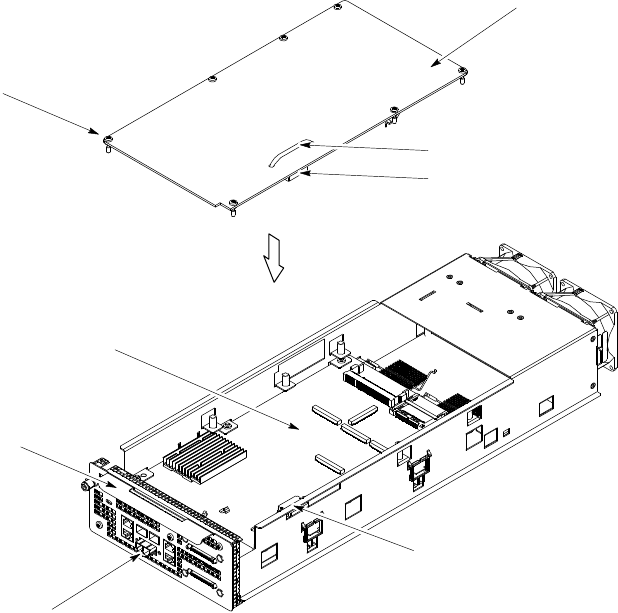
Modem Boards Chapter 8: DMI R eplacement Procedures
Figure 8 -3 shows the DMI assembly with its bottom side up for access to Modem 1.
Figure 8 -3 R emo ving and installing Modem 1
ti-cdma-06168.eps
7X
Captive Screws
Modem 1
Front Panel
HD MEZZ Connector
Modem Connector Handle
HD MEZZ Connector
Controller Board
Handle
8 -28 68P09283A64 -3
FOA SEP 2007
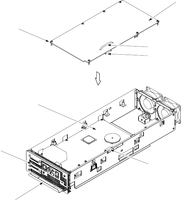
1X UBS Macro B T S FRU Modem Boards
Figure 8 -4 shows the DMI assembly with its top side up for access to Modem 2.
Figure 8 -4 R emo ving and installing Modem 2
ti-cdma-06169.eps
7X
Captive Screws
Modem 2
Front Panel
HD MEZZ Connector
Modem Connector Handle
HD MEZZ Connector
Controller Board
Handle
Optimization Recommended
P erform the following BTS Optimization/A TP procedures:
68P09283A64 -3 8 -29
FOA SEP 2007
Modem Boards Chapter 8: DMI R eplacement Procedures
•BTS Device Database Audit
•BTS Device Database Update
•Timing Initialization/V erification
•TX P ath Calibration Audit
•Spectral Purity TX Mask A TP (optional)
•W aveform Quality (Rho) A TP (optional)
•Code Domain P ower A TP (optional)
•FER T est
•Alarm V erification
Refer to the
1X UBS Macro BTS Optimization/A TP
manual for the optimization procedures.
8 -30 68P09283A64 -3
FOA SEP 2007

C h a p t e r
9
PDU Replacement Procedures■■■■■■■■■■■■■■■■■■■■■■■■■■■■■■■■■■■■■■■■■■■■■■■■■■■■■■■■■■■■■■
■
■
■
■
68P09283A64 -3 9 -1
SEP 2007 FOA

P ower Distribution Unit (PDU) Chapter 9: PDU R eplacement Procedures
Power Distribution Unit (PDU)■■■■■■■■■■■■■■■■■■■■■■■■■■■■■■■■■■■■■■■■■■■■■■■■■■■■■■■■■■■■■■
■
■
PDU Description
The PDU distributes +27 V DC output operating power to the UBS Macro BTS frame electronics.
The PDU is located near the bottom of the UBS Macro BTS frame. Figure 1 -1 UBS Macro BTS
low -tier/low -capacity frame (1000 mm rack) on page 1 - 27 ,Figure 1 -2 Low capacity UBS Macro
BTS starter frame (1800 mm rack) on page 1 - 28 and Figure 1 -3 UBS Macro BTS mid -capacity
frame (1800 mm rack) on page 1 - 30 show the location of the PDU within the UBS Macro BTS
frame.
Figure 1 -12 PDU front panel detail on page 1 - 42 shows the location of +27 V DC output power
connectors and circuit breakers on the front of the PDU .
Figure 1 -13 PDU rear panel detail on page 1 - 43 shows the location of +27 V DC input power
cable/connector and +27 V DC input filter capacitor on the rear of the PDU .
The PDU filters the +27 V DC input power and then splits the filtered +27 V DC input power
into +27 V DC branch circuits. Each branch circuit may be equipped with an integrated
circuit breaker and +27 V DC output power connector . Distribution is via output power cables
connected between the PDU +27 V DC output power connectors and the corresponding
equipment +27 V DC input power connector .
The circuit breakers provide current overload protection for the +27 V DC branch circuits
distributed to the corresponding UBS Macro BTS equipment. The circuit breakers also provide
ON/OFF switching of the +27 V DC output operating power to the corresponding equipment.
The PDU is shipped with the 1st +27 V DC input power cable/connector and filter
capacitor installed. The 2nd +27 V DC input power cable/connector and filter
capacitor are installed, on site, when a 3rd XMI is added to the frame.
The PDU is shipped with a circuit breaker and +27 V DC output power connector
installed for: XMI 1, DMI 1, DMI 2 and S SI 1. When other equipment is added to the
frame, the corresponding circuit breaker and +27 V DC output power connector
is installed on site.
9 -2 68P09283A64 -3
FOA SEP 2007

1X UBS Macro B T S FRU P ower Distribution Unit (PDU)
The PDU contains the following:
•Internal DC input reverse polarity/over -voltage/surge protection, filtering, input/output
bus bars.
•Up to two DC input power cables/connectors for +27 V DC input to the rear of the PDU .
•PDU front panel with cutouts for integrated circuit breaker and +27 V DC output power
connectors. There are cutouts for the following circuit breakers/power connectors:
F our 90A circuit breakers/power connectors for XMI 1 through XMI 4.
Five 20A circuit breakers/power connectors for DMI 1 through DMI 5.
T wo 20A circuit breakers/power connectors for S SI 1 and S SI 2.
T wo 10A circuit breakers/power connectors for ACC 1 and ACC 2. Each ACC branch
circuit has three DC power connectors. Up to three accessories can share the 10A
branch circuit.
System impact/considerations
P erforming this replacement procedure will cause BTS downtime and interrupt all
call processing.
Prior to replacing the PDU , the UBS Macro BTS site signaling is shutdown (i.e., disable the BTS
site) then the UBS Macro BTS frame is powered down.
Table 9 -1 PDU R eplacement Conditions
FRU
Ref Designator What to Shutdown...
P ower Distribution
Unit (PDU)
PDU
Shutdown site signaling functions and then power
down the frame.
Required items
Documents
•
1X UBS Macro BTS Optimization/A TP
manual.
68P09283A64 -3 9 -3
FOA SEP 2007
P ower Distribution Unit (PDU) Chapter 9: PDU R eplacement Procedures
Tools
•10 mm socket and ratchet
•T orque driver
•T25 TORX driver
Torque requirements
•PDU mounting screws; 4.77 N -m (42 in -lb)
Replacement unit
•PDU (Motorola model STPN4038)
Prerequisites
Coordinate this repair task with the OMCR operator .
Before you begin
Before you begin, record the pertinent information in T able 9 -2 .
Table 9 -2 Item number replacement list
Item
Number
BTS number
F ailed PDU
PDU replacement procedure
This procedure requires working on or around circuitry which is extremely sensitiv e
to ESD . W ear a conductiv e, high impedance wrist str ap during the procedure. Use
appropriate safet y measures.
9 -4 68P09283A64 -3
FOA SEP 2007
1X UBS Macro B T S FRU P ower Distribution Unit (PDU)
T o replace the PDU perform Procedure 9 -1 and then Procedure 9 -2 .
Procedure 9 -1 R emo ving the failed PDU
A T THE OMCR
1
Shut down site signaling functions according to Procedure 3-2 Shutdown site signaling
functions procedure for a packet BTS on page 3- 5 .
A T THE BTS SITE
2
P ower down the UBS Macro BTS frame according to the section: P owering Down the
Frame on page 2- 3 .
Mak e sure the facilit y circuit break er controlling external AC or DC power , whichev er
is applicable, to the UBS Macro B T S fr ame is set to the OFF position.
Y ou will be disconnecting multiple cables from connectors. If necessary , use
masking tape and a marker and temporarily tag each cable as to the proper
connector before disconnection.
3
Disconnect the +27 V DC output power cable from the +27 V DC input power cable on the
rear of the PDU by separating the orange connectors.
4
Disconnect all of the cables connected to the PDU front panel connectors.
5
If UBS Macro BTS frame is equipped with carrier strips go to step 6 .
If UBS Macro BTS frame is not equipped with carrier strips go to step 7 .
6
Remove the carrier strips from the frame as follows:
•Using a 10 mm socket and ratchet, loosen and remove the 8 nuts that secure each
carrier strip to the frame.
•Remove the carrier strip.
7
Loosen the two rack mounting screws in the keyhole slots of the PDU rack mounting flanges.
Do not remove these two screws. Leave the screw heads extending 8 mm out from the rack
surface. These two screws will serve as hanger screws.
8
Completely loosen and remove the remaining two rack mounting screws in the PDU rack
mounting flanges.
9
Grasp the PDU and lift it up and off of the hanger screws. Pull the PDU out of the rack
and set it out of the way .
68P09283A64 -3 9 -5
FOA SEP 2007

P ower Distribution Unit (PDU) Chapter 9: PDU R eplacement Procedures
Procedure 9 -2 Installing the replacement PDU
A T THE BTS SITE
1
Properly position the replacement PDU in the rack location.
Align the keyhole slots of the PDU mounting flanges with the two hanger screws and
hang the replacement PDU on the rack.
2
Insert screws in the two open slots of the PDU rack mounting flanges.
Tighten all four PDU rack mounting screws to 4.77 N-m (42 in-lb).
3
Reconnect all applicable cables to the PDU front panel connectors.
4
Connect the +27 V DC output power cable to the +27 V DC input power cable on the rear of
the PDU by mating the orange connectors.
5
P ower up the UBS Macro BTS frame according to the section: P ower-up the Frame on
page 2- 3 .
There is no optimization required for the PDU replacement.
A T THE OMCR
6
Restore site signaling operations according to Procedure 3-3 Restore site signaling
operations procedure for a packet BTS on page 3- 10 .
9 -6 68P09283A64 -3
FOA SEP 2007

1X UBS Macro B T S FRU Break er Module Assembly (BMA)
Breaker Module Assembly (BMA)■■■■■■■■■■■■■■■■■■■■■■■■■■■■■■■■■■■■■■■■■■■■■■■■■■■■■■■■■■■■■■
■
■
BMA Description
The BMA is an integrated circuit breaker and output power connector . The circuit breaker
provides current overload protection for the output power connector .
The BMAs are located on the PDU front panel (see Figure 1 -12 PDU front panel detail on page
1 - 42 .)
The BMAs provide current overload protection for the +27 V DC branch circuits distributed
to the corresponding UBS Macro BTS equipment. The circuit breakers also provide ON/OFF
switching of the +27 V DC output operating power to the corresponding equipment.
The PDU in the UBS Macro BTS may be equipped with the following BMAs:
•up to four 90A for XMI 1 – XMI 4.
•up to five 20A for DMI 1 – DMI 5.
•up to two 20A for S SI 1 – S SI 2.
•up to two 10A for ACC 1 – ACC 2. This BMA has three output power connectors for
accessories.
The actual BMA equipage in the PDU is customer dependent.
Each BMA is arranged so that the circuit breaker is just below the corresponding DC output
power connector .
The PDU front panel cover must be removed to gain access to the BMAs (see Figure 9 -1 PDU
Front P anel Removal/Installation Detail on page 9 - 12 .)
Each BMA is screw mounted to the PDU output bus bars (i.e., +27 V DC and –0 V DC). This
physical mounting provides electrical contact between the bus bars and the BMA. Refer to
Figure 9 -2 PDU Front P anel (cover removed) on page 9 - 12 for BMA screw mounting details.
System impact/considerations
P erforming this replacement procedure will cause BTS downtime and interrupt all
call processing.
68P09283A64 -3 9 -7
FOA SEP 2007

Break er Module Assembly (BMA) Chapter 9: PDU R eplacement Procedures
Prior to replacing a BMA, the UBS Macro BTS site signaling is shutdown (i.e., disable the BTS
site) then the UBS Macro BTS frame is powered down.
Table 9 -3 PDU R eplacement Conditions
FRU
Ref Designator What to Shutdown...
Breaker Module
Assembly (BMA)
XMI 1 – XMI 4, DMI
1 – DMI 5, S SI 1 –
S SI 2, ACC 1 – ACC
2
Shutdown site signaling functions and then power
down the frame.
Required items
Documents
•
1X UBS Macro BTS Optimization/A TP
manual.
Tools
•T orque driver
•T25 TORX driver
Torque requirements
•BMA mounting screws; 4.8 N -m (42.25 in -lb) ±10%
Replacement unit
•90A BMA (Motorola model STLN4093), for XMIs
•20A BMA (Motorola model STLN6472), for DMIs and S SIs
•10A BMA (Motorola model STLN6475), for ACCs
Mounting screws are provided with each BMA; four screws with the 90A BMA,
two screws with the 20A BMA and two screws with the 10A BMA.
9 -8 68P09283A64 -3
FOA SEP 2007
1X UBS Macro B T S FRU Break er Module Assembly (BMA)
Prerequisites
Coordinate this repair task with the OMCR operator .
Before you begin
Before you begin, record the pertinent information in T able 9 -4 .
Table 9 -4 Item number replacement list
Item
Number
BTS number
F ailed BMA
BMA replacement procedure
BMA mounting screws must be tightened to the specied torque to prev ent arcing
and possible re hazard.
T o replace a BMA perform Procedure 9 -3 and then Procedure 9 -4 .
Procedure 9 -3 R emo ving the failed BMA
A T THE OMCR
1
Shut down site signaling functions according to Procedure 3-2 Shutdown site signaling
functions procedure for a packet BTS on page 3- 5 .
A T THE BTS SITE
2
P ower down the UBS Macro BTS frame according to the section: P owering Down the
Frame on page 2- 3 .
Continued
68P09283A64 -3 9 -9
FOA SEP 2007
Break er Module Assembly (BMA) Chapter 9: PDU R eplacement Procedures
Procedure 9 -3 R emo ving the failed BMA (Continued)
Mak e sure the facilit y circuit break er controlling external AC or DC power , whichev er
is applicable, to the UBS Macro B T S fr ame is set to the OFF position.
Y ou will be disconnecting multiple cables from connectors. If necessary , use
masking tape and a marker and temporarily tag each cable as to the proper
connector before disconnection.
3
Set all PDU front panel circuit breakers to the off (pulled out) position.
4
Disconnect all DC power cables from the PDU front panel. Dress these cables away from
the PDU front panel.
5
Remove the PDU front panel as follows:
•See Figure 9-1 PDU Front P anel Removal/Installation Detail on page 9- 12 .
•While depressing the front panel cover latch tab on the left and right front ends of the
PDU , slide the PDU front panel forward and off of the PDU .
6
Remove the BMA as follows:
•See Figure 9-2 PDU Front P anel (cover removed) on page 9- 12 .
•Locate the BMA to be removed.
•Using a TORX T25 driver , remove the BMA mounting screws.
•Remove the BMA from the PDU .
Procedure 9 -4 Installing the replacement BMA
A T THE BTS SITE
1
BMA mounting screws must be tightened to the specied torque to prev ent arcing
and possible re hazard.
Install the replacement BMA as follows:
•See Figure 9-2 PDU Front P anel (cover removed) on page 9- 12 .
Continued
9 -10 68P09283A64 -3
FOA SEP 2007

1X UBS Macro B T S FRU Break er Module Assembly (BMA)
Procedure 9 -4 Installing the replacement BMA (Continued)
•Properly position the replacement BMA on the PDU output bus bars.
•Align the BMA screw holes with the appropriate screw holes on the PDU output bus
bars.
•Insert the mounting screws.
•Using a TORX T25 driver , tighten all BMA mounting screws to 4.8 N-m (42.25 in-lb).
2
Reattach the PDU front panel cover to the PDU as follows:
•See Figure 9-1 PDU Front P anel Removal/Installation Detail on page 9- 12 .
•Align the PDU front panel cover with the PDU circuit breaker actuators and power
connectors while inserting the PDU front panel cover latch tabs into the retainer on
the left and right front ends of the PDU .
•Slide the PDU front panel cover onto the front of the PDU .
•Firmly press on the ends of the PDU front panel until each end tab snaps into place.
3
Set all PDU front panel circuit breakers to the off (pulled out) position.
4
Reconnect all applicable cables to the PDU front panel connectors. Make sure that each
cable is connected to the proper PDU front panel power connector .
5
P ower up the UBS Macro BTS frame according to the section: P ower-up the Frame on
page 2- 3 .
There is no optimization required for the BMA replacement.
A T THE OMCR
6
Restore site signaling operations according to Procedure 3-3 Restore site signaling
operations procedure for a packet BTS on page 3- 10 .
Reference diagrams
Figure 9 -1 shows details for removing and installing the PDU front cover . Figure 9 -2 shows
BMA mounting details.
68P09283A64 -3 9 -11
FOA SEP 2007
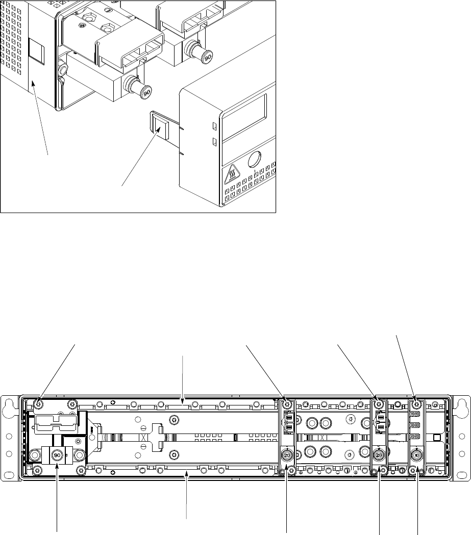
Break er Module Assembly (BMA) Chapter 9: PDU R eplacement Procedures
Figure 9 -1 PDU Front P anel R emo v al/Installation Detail
ti-cdma-06382.eps
Front Panel
Cover Latch Tab
PDU
Figure 9 -2 PDU Front P anel (co v er remo v ed)
ti-cdma-06383.eps
4X
Mounting Screws
2X
Mounting Screws 2X
Mounting Screws
2X
Mounting Screws
DMI 20A BMA SSI 20A BMA ACC 10A BMAXMI 90A BMA
+27 V DC Bus Bar
-0 V DC Bus Bar
NOTE:
1. This diagram shows mounting details for each kind of BMA.
It does not to show the exact BMA equipage.
9 -12 68P09283A64 -3
FOA SEP 2007

C h a p t e r
1 0
PSM Shelf Replacement Procedures■■■■■■■■■■■■■■■■■■■■■■■■■■■■■■■■■■■■■■■■■■■■■■■■■■■■■■■■■■■■■■
■
■
■
■
68P09283A64 -3 10 -1
SEP 2007 FOA
–48 V DC P ower Supply Module (PSM) Shelf Chapter 10: PSM Shelf R eplacement Procedures
–48 V DC Power Supply Module (PSM) Shelf■■■■■■■■■■■■■■■■■■■■■■■■■■■■■■■■■■■■■■■■■■■■■■■■■■■■■■■■■■■■■■
■
■
–48 V DC PSM Shelf Description
The –48 V DC P ower Supply Module (PSM) shelf is optional. It is used to convert –48 V DC
input power to +27V DC output operating power for distribution to the UBS Macro BTS frame
electronics.
The –48 V DC PSM shelf is located at the bottom of the UBS Macro BTS frame. Figure 1 -1 UBS
Macro BTS low -tier/low -capacity frame (1000 mm rack) on page 1 - 27 ,Figure 1 -2 Low capacity
UBS Macro BTS starter frame (1800 mm rack) on page 1 - 28 and Figure 1 -3 UBS Macro BTS
mid -capacity frame (1800 mm rack) on page 1 - 30 show the location of the –48 V DC PSM shelf
within the UBS Macro BTS frame.
Figure 1 -15 –48 V DC and 220 V AC PSM shelves front panel detail on page 1 - 46 shows the
location of I/O port connectors and PSM slots on the front of the –48 V DC PSM shelf .
Figure 1 -16 –48 V DC PSM shelf rear panel detail on page 1 - 47 shows the location of input
connector and output cable on the rear of the –48 V DC PSM shelf .
The –48 V DC PSM shelf provides interconnection between the PSM slots DC I/O and the PSM
shelf DC I/O as well as interconnection between the PSM slots alarm/status I/O and the PSM
shelf alarm & control I/O .
The plug -in PSMs provide DC -DC conversion and +27V DC power output capabilities.
Up to three PSMs can be housed in the PSM shelf . A minimum of two PSMs are equipped for
redundancy . An empty PSM 3 slot is covered with a filler panel.
PSM shelf plug -in modules
The –48 V DC PSM is a DC–DC converter . It operates from a nominal –48 V DC (–39 to –72 V)
input and provides a 2700 W , +27 V DC (+/– 0.1 V) output. The output is designed to support
load current sharing when configured for parallel output operation with other –48 V DC PSMs.
Three PSMs can provide a maximum of 8100 W , +27 V DC (+/– 0.1 V) output from the –48 V
DC PSM shelf .
Each PSM has internal fans that circulate cooling air from the front to the rear of the module.
Each PSM slides into a slot in the shelf . Blade type contacts, on the rear of the PSM, mate with
the DC I/O bus bar contacts in the PSM slot.
10 -2 68P09283A64 -3
FOA SEP 2007

1X UBS Macro B T S FRU –48 V DC P ower Supply Module (PSM) Shelf
PSM shelf DC I/O interconnection
Each PSM slot in the –48 V DC PSM shelf has two contacts (– feed and + return) for 48 V DC
input and two contacts (+ feed and – return) for +27 V DC output.
The –48 V DC PSM shelf has DC I/O bus bars at the rear of the shelf . The 48 V DC input contacts
of the three PSM slots are parallel connected to the DC input bus bars. The +27 V DC output
contacts of the three PSM slots are parallel connected to DC input bus bars.
The DC input bus bars are interconnected to the –48 V DC input power connector on the rear of
the PSM shelf .
The DC output bus bars are interconnected to the +27 V DC output power cable on the rear
of the PSM shelf . This cable connects to the +27 V DC input power cable on the rear of the
UBS Macro PDU . The PDU distributes the +27V DC operating power to the UBS Macro frame
electronics.
PSM shelf alarm and control I/O interconnection
Each PSM slot has a bulkhead connector . The I/O signals of each of these slot connectors are
interconnected to the ALARM & CONTROL connector on the front of the –48 V DC PSM shelf .
Each –48 V DC PSM has a rear panel status/alarm drawer connector that mates with the
bulkhead connector in the PSM slot of the PSM shelf . The I/O signals of this connector are
interconnected to the ALARM & CONTROL connector on the front of the –48 V DC PSM shelf .
This connector is cabled to the S SI front panel PSM connector . This allows the PSM alarm &
status to be monitored by the S SI. It also allows the front panel LEDs and module enable to
be controlled by the S SI.
PSM alarm & status signal inputs are current share, temp alarm, converter fail, fan fail, high
temp, low bus voltage, input voltage loss, presence, and EID .
The current share signal goes directly from one PSM to the others via PSM shelf backplane
looping without going to the S SI. Based on PSM alarm & status, the S SI outputs signals to
control the state of the LEDs.
The PSM shelf ALARM & CONTROL cable also contains the PSM enable line which
must be grounded at the S SI in order for the PSM to operate.
System impact/considerations
P erforming this replacement procedure will cause BTS downtime and interrupt all
call processing.
68P09283A64 -3 10 -3
FOA SEP 2007

–48 V DC P ower Supply Module (PSM) Shelf Chapter 10: PSM Shelf R eplacement Procedures
Prior to replacing the –48 V DC PSM shelf , the UBS Macro BTS site signaling is shutdown (i.e.,
disable the BTS site) then the UBS Macro BTS frame is powered down.
Table 10 -1 –48 V DC PSM Shelf R eplacement Conditions
FRU
Ref Designator What to Shutdown...
–48 V DC P ower
Supply Module
(PSM) shelf
–48 V DC PSM shelf Shutdown site signaling functions and then power
down the frame.
Required items
Documents
•
1X UBS Macro BTS Optimization/A TP
manual.
Tools
•T orque driver
•T25 TORX driver
Torque requirements
•PSM shelf mounting screws; 4.77 N -m (42 in -lb)
•PSM captive M4 retaining thumbscrew , 2.37 N -m (21 in -lb)
Replacement unit
•–48 V DC PSM shelf assembly (Motorola model STHN4089)
Prerequisites
Coordinate this repair task with the OMCR operator .
10 -4 68P09283A64 -3
FOA SEP 2007

1X UBS Macro B T S FRU –48 V DC P ower Supply Module (PSM) Shelf
Before you begin
Before you begin, record the pertinent information in T able 10 -2 .
Table 10 -2 Item number replacement list
Item
Number
BTS number
F ailed –48 V DC PSM shelf
number
–48 V DC PSM shelf replacement procedure
This procedure requires working on or around circuitry which is extremely sensitiv e
to ESD . W ear a conductiv e, high impedance wrist str ap during the procedure. Use
appropriate safet y measures.
T o replace the –48 V DC PSM shelf perform Procedure 10 -1 and then Procedure 10 -2 .
Procedure 10 -1 R emo ving the failed –48 V DC PSM shelf
A T THE OMCR
1
Shut down site signaling functions according to Procedure 3-2 Shutdown site signaling
functions procedure for a packet BTS on page 3- 5 .
A T THE BTS SITE
2
P ower down the –48 V DC UBS Macro BTS frame according to the section: P owering Down
the Frame on page 2- 3 .
Mak e sure the facilit y circuit break er controlling external 48 V DC power to the –48
V DC PSM shelf is set to the OFF position.
3
Using a T25 TORX bit and driver , loosen the captive retaining thumbscrews on all of the PSM
modules until the thumbscrews are disengaged from the shelf .
Continued
68P09283A64 -3 10 -5
FOA SEP 2007
–48 V DC P ower Supply Module (PSM) Shelf Chapter 10: PSM Shelf R eplacement Procedures
Procedure 10 -1 R emo ving the failed –48 V DC PSM shelf (Continued)
4
PSM weighs appro ximately 5 kg. Be careful when handling the PSM to prev ent
damage to the equipment and personal injury .
Remove all the PSMs from the slots of the –48 V DC PSM shelf .
Grasp the handle on the front panel of the PSM with one hand. Slowly pull the PSM out of
the shelf slot while carefully supporting the bottom of the module with the other hand.
5
Remove the filler panels (if used) from the slots of the –48 V DC PSM shelf . Using a T25
TORX bit and driver , loosen the captive retaining thumbscrew on the filler panel until it is
disengaged from the shelf .
Y ou will be disconnecting multiple cables from connectors. If necessary , use
masking tape and a marker and temporarily tag each cable as to the proper
connector before disconnection.
6
Disconnect the +27 V DC output power cable on the rear of the PSM shelf from the +27 V
DC input power cable on the rear of the PDU by separating the orange connectors.
7
Disconnect the –48 V DC input power cable from the rear of the –48 V DC PSM shelf by
separating the blue connectors.
8
Disconnect all of the cables connected to the –48 V DC PSM shelf front panel connectors.
9
Loosen the two rack mounting screws in the keyhole slots of the –48 V DC PSM shelf rack
mounting flanges. Do not remove these two screws. Leave the screw heads extending 8 mm
out from the rack surface. These two screws will serve as hanger screws.
10
Completely loosen and remove the remaining rack mounting screws in the –48 V DC PSM
shelf rack mounting flanges.
1 1
Grasp the –48 V DC PSM shelf and lift it up and off of the hanger screws. Pull the –48 V DC
PSM shelf out of the rack and set it out of the way .
Procedure 10 -2 Installing the replacement –48 V DC PSM shelf
A T THE BTS SITE
1
Properly position the replacement –48 V DC PSM shelf in the rack location.
Align the keyhole slots of the PSM shelf rack mounting flanges with the two hanger screws
and hang the shelf on the rack.
2
Insert screws in the 6 open slots of the PSM shelf rack mounting flanges.
Tighten all 8 PSM shelf rack mounting screws to 4.77 N-m (42 in-lb).
Continued
10 -6 68P09283A64 -3
FOA SEP 2007

1X UBS Macro B T S FRU –48 V DC P ower Supply Module (PSM) Shelf
Procedure 10 -2 Installing the replacement –48 V DC PSM shelf (Continued)
3
Reinstall all of the PSMs.
Properly orient each PSM and insert it into the appropriate PSM shelf slot.
Slowly slide the module into the shelf until the rear connectors are fully seated.
Make sure that the PSM is fully engaged with the shelf backplane slot connectors.
4
Using a T25 TORX bit and torque driver , tighten the captive retaining thumbscrews of
each PSM to 2.37 N-m (21 in-lb).
5
Reinstall filler panels over any empty PSM slots of the –48 V DC PSM shelf .
Using a T25 TORX bit and driver , tighten the captive retaining thumbscrew on the filler
panel to 2.37 N-m (21 in-lb).
6
Reconnect all applicable cables to the –48 V DC PSM shelf front panel connectors.
7
Connect the –48 V DC input power cable to the rear of the –48 V DC PSM shelf by mating
the blue connectors.
8
Connect the +27 V DC output power cable on the rear of the PSM shelf to the +27 V DC
input power cable on the rear of the PDU by mating the orange connectors.
9
P ower up the –48 V DC UBS Macro BTS frame according to the section: P ower-up the
Frame on page 2- 3 .
10
Observe the LEDs on the front of the PSMs.
The green LED should be on and the red LED should be off . This indicates normal operation.
There is no optimization required for the PSM shelf replacement.
A T THE OMCR
1 1
Restore site signaling operations according to Procedure 3-3 Restore site signaling
operations procedure for a packet BTS on page 3- 10 .
68P09283A64 -3 10 -7
FOA SEP 2007
220 V AC P ower Supply Module (PSM) Shelf Chapter 10: PSM Shelf R eplacement Procedures
220 V AC Power Supply Module (PSM) Shelf■■■■■■■■■■■■■■■■■■■■■■■■■■■■■■■■■■■■■■■■■■■■■■■■■■■■■■■■■■■■■■
■
■
220 V AC PSM Shelf Description
The 220 V AC P ower Supply Module (PSM) shelf is optional. It is used to convert 220 V AC
input power to +27V DC output operating power for distribution to the UBS Macro BTS frame
electronics.
The 220 V AC PSM shelf is located at the bottom of the UBS Macro BTS frame. Figure 1 -1 UBS
Macro BTS low -tier/low -capacity frame (1000 mm rack) on page 1 - 27 ,Figure 1 -2 Low capacity
UBS Macro BTS starter frame (1800 mm rack) on page 1 - 28 and Figure 1 -3 UBS Macro BTS
mid -capacity frame (1800 mm rack) on page 1 - 30 show the location of the 220 V AC PSM shelf
within the UBS Macro BTS frame.
Figure 1 -15 –48 V DC and 220 V AC PSM shelves front panel detail on page 1 - 46 shows the
location of I/O port connectors and PSM slots on the front of the 220 V AC PSM shelf .
Figure 1 -17 220 V AC PSM shelf rear panel detail on page 1 - 48 shows the location of input
connector and output cable/connector on the rear of the 220 V AC PSM shelf .
The 220 V AC PSM shelf provides interconnection between the PSM slots AC input/DC output
and the PSM shelf AC input/DC output as well as interconnection between the PSM slots
alarm/status I/O and the PSM shelf alarm & control I/O .
The plug -in PSMs provide AC -DC conversion and +27V DC power output capabilities.
Up to three PSMs can be housed in the PSM shelf . A minimum of two PSMs are equipped for
redundancy . An empty PSM 3 slot is covered with a filler panel.
PSM shelf plug -in modules
The 220 V AC PSM is an AC–DC power supply . It contains AC line input filtering and AC–DC
rectification. The rectifier output is applied to a DC–DC converter .
The 220 V AC PSM operates from a nominal 220 V AC (154 to 300 V) input and provides a 2700
W , +27 V DC (+/– 0.1 V) output. The output is designed to support load current sharing when
configured for parallel output operation with other 220 V AC PSMs.
Three PSMs can provide a maximum of 8100 W , +27 V DC (+/– 0.1 V) output from the 220 V
AC PSM shelf .
Each PSM has internal fans that circulate cooling air from the front to the rear of the module.
Each PSM slides into a slot in the PSM shelf . The AC input & status/alarm drawer connector , on
the rear of the PSM, mates with a bulkhead connector in the PSM slot. Also blade type contacts,
on the rear of the PSM, mate with the DC output bus bar contacts in the PSM slot.
10 -8 68P09283A64 -3
FOA SEP 2007
1X UBS Macro B T S FRU 220 V AC P ower Supply Module (PSM) Shelf
PSM shelf AC input interconnection
Each PSM slot in the 220 V AC PSM shelf has a bulkhead connector . The 220 V AC line input pins
from the bulkhead connector of the three PSM slots are parallel connected to the AC input buses.
Each 220 V AC PSM has a rear panel AC input & status/alarm drawer connector that mates with
a bulkhead connector in the PSM slot of the 220 V AC PSM shelf .
The AC line input buses in the 220 V AC PSM shelf are connected to the AC input terminal block
on the rear of the 220 V AC PSM shelf . This terminal block is wired to the AC input lines.
The 220 V AC PSM shelf and 220 V AC PSMs can operate with any one of the following AC
power inputs:
•Single -Phase
•3 -Phase ST AR
•3 -Phase DEL T A
PSM shelf DC output interconnection
Each PSM slot in the 220 V AC PSM shelf has two contacts (+ feed and – return) for +27 V
DC output.
The 220 V AC PSM shelf has DC output bus bars at the rear of the shelf . The +27 V DC output
contacts of the three PSM slots are parallel connected to DC input bus bars.
The DC input bus bars are interconnected to the 220 V AC input power connector on the rear of
the PSM shelf .
The DC output bus bars are interconnected to the +27 V DC output power cable on the rear
of the PSM shelf . This cable connects to the +27 V DC input power cable on the rear of the
UBS Macro PDU . The PDU distributes the +27V DC operating power to the UBS Macro frame
electronics.
In addition, the DC output bus bars are interconnected to the +27 V DC output power connector
on the rear of the 220 V AC PSM shelf . Usage of this connector is optional. It can be cabled to
back -up batteries for battery charging purposes.
68P09283A64 -3 10 -9
FOA SEP 2007

220 V AC P ower Supply Module (PSM) Shelf Chapter 10: PSM Shelf R eplacement Procedures
PSM shelf alarm and control I/O interconnection
Each PSM slot has a bulkhead connector . The status/alarm I/O signals of each of these slot
connectors are interconnected to the ALARM & CONTROL connector on the front of the 220 V
AC PSM shelf .
Each 220 V AC PSM has a rear panel status/alarm drawer connector that mates with the
bulkhead connector in the PSM slot of the PSM shelf . The I/O signals of this connector are
interconnected to the ALARM & CONTROL connector on the front of the 220 V AC PSM shelf .
This connector is cabled to the S SI front panel PSM connector . This allows the PSM alarm &
status to be monitored by the S SI. It also allows the front panel LEDs and module enable to
be controlled by the S SI.
PSM alarm & status signal inputs are current share, temp alarm, converter fail, fan fail, high
temp, low bus voltage, input voltage loss, presence, and EID .
The current share signal goes directly from one PSM to the others via PSM shelf backplane
looping without going to the S SI. Based on PSM alarm & status, the S SI outputs signals to
control the state of the LEDs.
The PSM shelf ALARM & CONTROL cable also contains the PSM enable line which
must be grounded at the S SI in order for the PSM to operate.
System impact/considerations
P erforming this replacement procedure will cause BTS downtime and interrupt all
call processing.
Prior to replacing the 220 V AC PSM shelf , the UBS Macro BTS site signaling is shutdown (i.e.,
disable the BTS site) then the UBS Macro BTS frame is powered down.
Table 10 -3 220 V AC PSM Shelf R eplacement Conditions
FRU
Ref Designator What to Shutdown...
220 V AC P ower
Supply Module
(PSM) shelf
220 V AC PSM shelf Shutdown site signaling functions and then power
down the frame.
10 -10 68P09283A64 -3
FOA SEP 2007

1X UBS Macro B T S FRU 220 V AC P ower Supply Module (PSM) Shelf
Required items
Documents
•
1X UBS Macro BTS Optimization/A TP
manual.
Tools
•T orque driver
•T25 TORX driver
•T20 TORX bit with 12 -inch extension
•Flat blade screwdriver
Torque requirements
•PSM shelf mounting screws; 4.77 N -m (42 in -lb)
•PSM captive M4 retaining thumbscrew , 2.37 N -m (21 in -lb)
•T erminal block cover box screws, 1.6 - 1.8 N -m (14 - 16 in -lb)
Replacement unit
•220 V AC PSM shelf assembly (Motorola model STHN4092)
Prerequisites
Coordinate this repair task with the OMCR operator .
68P09283A64 -3 10 -11
FOA SEP 2007
220 V AC P ower Supply Module (PSM) Shelf Chapter 10: PSM Shelf R eplacement Procedures
Before you begin
Before you begin, record the pertinent information in T able 10 -4 .
Table 10 -4 Item number replacement list
Item
Number
BTS number
F ailed 220 V AC PSM shelf
number
220 V AC PSM shelf replacement procedure
This procedure requires working on or around circuitry which is extremely sensitiv e
to ESD . W ear a conductiv e, high impedance wrist str ap during the procedure. Use
appropriate safet y measures.
T o replace the 220 V AC PSM shelf perform Procedure 10 -3 and then Procedure 10 -4 .
Procedure 10 -3 R emo ving the failed 220 V AC PSM shelf
A T THE OMCR
1
Shut down site signaling functions according to Procedure 3-2 Shutdown site signaling
functions procedure for a packet BTS on page 3- 5 .
A T THE BTS SITE
2
P ower down the 220 V AC UBS Macro BTS frame according to the section: P owering Down
the Frame on page 2- 3 .
Mak e sure the facilit y circuit break er controlling external 220 V AC power to the
220 V AC PSM shelf is set to the OFF position.
3
Using a T25 TORX bit and driver , loosen the captive retaining thumbscrews on all of the PSM
modules until the thumbscrews are disengaged from the shelf .
Continued
10 -12 68P09283A64 -3
FOA SEP 2007
1X UBS Macro B T S FRU 220 V AC P ower Supply Module (PSM) Shelf
Procedure 10 -3 R emo ving the failed 220 V AC PSM shelf (Continued)
4
PSM weighs appro ximately 5 kg. Be careful when handling the PSM to prev ent
damage to the equipment and personal injury .
Remove all the PSMs from the slots of the 220 V AC PSM shelf .
Grasp the handle on the front panel of the PSM with one hand. Slowly pull the
PSM out of the shelf slot while carefully supporting the bottom of the module with the
other hand.
5
Remove the filler panels (if used) from the slots of the 220 V AC PSM shelf . Using a T25
TORX bit and driver , loosen the captive retaining thumbscrew on the filler panel until it is
disengaged from the shelf .
Y ou will be disconnecting multiple cables/wires from connectors. If necessary ,
use masking tape and a marker and temporarily tag each cable as to the proper
connector before disconnection.
6
Disconnect the +27 V DC output power cable on the rear of the PSM shelf from the +27 V
DC input power cable on the rear of the PDU by separating the orange connectors.
7
Disconnect the back -up battery cable (if used) from the +27 V DC output power connector
on the rear of the 220 V AC PSM shelf by separating the orange connectors.
8
Using a TORX T20 bit and driver , remove the 4 screws securing the terminal block cover box
to the 220 V AC PSM shelf . Remove the terminal block cover box from the PSM shelf .
The terminal block cover box may have conduit attached to it. It may be necessary
to free the conduit so that the box can be moved out of the way .
9
Using a flat blade screwdriver , turn the ground terminal
screw counter clockwise (CCW) to open the terminal.
Disconnect the ground wire from the terminal.
10
Using a flat blade screwdriver , turn each AC supply line wire
terminal screw counter clockwise (CCW) to open the terminals.
Disconnect the AC supply line wires from the terminals.
1 1
Disconnect all of the cables connected to the 220 V AC PSM shelf front panel connectors.
12
Using TORX T25 driver , loosen the two rack mounting screws in the keyhole slots of the
220 V AC PSM shelf rack mounting flanges. Do not remove these two screws. Leave the
screw heads extending 8 mm out from the rack surface. These two screws will serve as
hanger screws.
Continued
68P09283A64 -3 10 -13
FOA SEP 2007

220 V AC P ower Supply Module (PSM) Shelf Chapter 10: PSM Shelf R eplacement Procedures
Procedure 10 -3 R emo ving the failed 220 V AC PSM shelf (Continued)
13
Using TORX T25 driver , completely loosen and remove the remaining rack mounting screws
in the 220 V AC PSM shelf rack mounting flanges.
14
Grasp the 220 V AC PSM shelf and lift it up and off of the hanger screws. Pull the 220 V AC
PSM shelf out of the rack and set it out of the way .
Procedure 10 -4 Installing the replacement 220 V AC PSM shelf
A T THE BTS SITE
1
Using a TORX T20 bit and driver , remove the 4 screws securing the terminal block cover
box to the rear of the replacement 220 V AC PSM shelf . Remove the terminal block cover
box from the PSM shelf .
2
Make sure that the AC line terminal block on the replacement 220 V AC PSM shelf is properly
configured with insertion bridging. It should match that of the failed 220 V AC PSM shelf .
If necessary , use a flat blade screwdriver to open terminals (turn screws CCW) for insertion
bridge placement. Place an insertion bridge into the proper terminals. While holding
the bridge with one hand, turn the corresponding terminal screws CW until the bridge
is securely clamped.
3
Properly position the replacement 220 V AC PSM shelf in the rack location.
Align the keyhole slots of the PSM shelf rack mounting flanges with the two hanger screws
and hang the shelf on the rack.
4
Insert screws in the 6 open slots of the PSM shelf rack mounting flanges.
Using TORX T25 driver , tighten all 8 PSM shelf screws to 4.77 N-m (42 in-lb).
5
Reinstall all of the PSMs.
Properly orient each PSM and insert it into the appropriate PSM shelf slot.
Slowly slide the module into the shelf until the rear connectors are fully seated.
Make sure that the PSM is fully engaged with the shelf backplane slot connectors.
6
Using a T25 TORX bit and torque driver , tighten the captive retaining thumbscrews of
each PSM to 2.37 N-m (21 in-lb).
7
Reinstall filler panels over any empty PSM slots of the 220 V AC PSM shelf .
Using a T25 TORX bit and driver , tighten the captive retaining thumbscrew on the filler
panel to 2.37 N-m (21 in-lb).
8
Reconnect all applicable cables to the 220 V AC PSM shelf front panel connectors.
9
Connect the 220 V AC input lines to the proper terminals on the
rear of the 220 V AC PSM shelf by performing the following:
•Use a flat blade screwdriver to open the terminals (turn screws CCW)
•Insert the appropriate wire into the terminal.
•While holding the wire with one hand, turn the corresponding terminal screw CW until
the wire is securely clamped. Tighten the terminal screw to 4.0 - 4.5 N-m (35 - 40 in-lb).
Continued
10 -14 68P09283A64 -3
FOA SEP 2007

1X UBS Macro B T S FRU 220 V AC P ower Supply Module (PSM) Shelf
Procedure 10 -4 Installing the replacement 220 V AC PSM shelf (Continued)
10
Using a flat blade screwdriver , turn the ground terminal screw counter clockwise (CCW)
until the terminal is fully open. Insert the earth ground wire into the ground terminal.
Turn the ground terminal screw clockwise (CW) to close the terminal and secure the wire.
Tighten the terminal screw to 4.0 - 4.5 N-m (35 - 40 in-lb).
1 1
Place the cover box, with conduit attached, in position over the AC input terminal block.
12
Insert the 4 screws to secure the cover box to the PSM shelf . Ensure that the wires are not
pinched.
13
Using a TORX T20 bit and driver , tighten the 4 screws to 1.6 - 1.8 N-m (14 - 16 in-lb).
14
Connect the back -up battery cable (if used) the +27 V DC output power connector on the
rear of the 220 V AC PSM shelf by mating the orange connectors.
15
Connect the +27 V DC output power cable on the rear of the PSM shelf to the +27 V DC
input power cable on the rear of the PDU by mating the orange connectors.
16
P ower up the 220 V AC UBS Macro BTS frame according to the section: P ower-up the
Frame on page 2- 3 .
17
Observe the LEDs on the front of the PSMs.
The green LED should be on and the red LED should be off . This indicates normal operation.
There is no optimization required for the PSM shelf replacement.
A T THE OMCR
18
Restore site signaling operations according to Procedure 3-3 Restore site signaling
operations procedure for a packet BTS on page 3- 10 .
68P09283A64 -3 10 -15
FOA SEP 2007

P ower Supply Modules (PSMs) Chapter 10: PSM Shelf R eplacement Procedures
Power Supply Modules (PSMs)■■■■■■■■■■■■■■■■■■■■■■■■■■■■■■■■■■■■■■■■■■■■■■■■■■■■■■■■■■■■■■
■
■
PSM Descriptions
Up to three PSMs can be housed in the PSM shelf . A minimum of two PSMs are equipped for
redundancy . An empty PSM 3 slot is covered with a filler panel. Refer to Figure 1 -15 –48 V DC
and 220 V AC PSM shelves front panel detail on page 1 - 46 .
There are two types of PSMs that can be used with the UBS Macro BTS PSM shelf . These
are as follows:
•–48 V DC PSM
•220 V AC PSM
The –48 V DC PSMs are only used in a –48 V DC PSM shelf .
The 220 V AC PSMs are only used in a 220 V AC PSM shelf .
Nev er plug a –48 V DC PSM into a 220 V AC PSM shelf .
Nev er plug a 220 V AC PSM into a -–48 V DC PSM shelf .
10 -16 68P09283A64 -3
FOA SEP 2007

1X UBS Macro B T S FRU P ower Supply Modules (PSMs)
–48 V DC PSM Description
The –48 V DC PSM is a DC–DC converter . It operates from a nominal –48 V DC (–39 to –72 V)
input and provides a 2700 W , +27 V DC (+/– 0.1 V) output. The output is designed to support
load current sharing when configured for parallel output operation with other –48 V DC PSMs.
The PSM has internal fans that circulate cooling air from the front to the rear of the module.
Each –48 V DC PSM slides into a slot in the –48 V DC PSM shelf . Blade type contacts, on the
rear of the –48 V DC PSM, mate with the DC input/output bus bars at the rear of the –48 V
DC PSM shelf .
Each –48 V DC PSM has a rear panel status/alarm drawer connector that mates with a bulkhead
connector in the PSM slot of the PSM shelf . The I/O signals of this connector are interconnected
to the ALARM & CONTROL connector on the front of the –48 V DC PSM shelf . This connector
is cabled to the S SI front panel PSM connector . This allows the PSM alarm & status to be
monitored by the S SI. It also allows the front panel LEDs and module enable to be controlled
by the S SI.
PSM alarm & status signal inputs are current share, temp alarm, converter fail, fan fail, high
temp, low bus voltage, input voltage loss, presence, and EID .
The current share signal goes directly from one PSM to the others via PSM shelf backplane
looping without going to the S SI. Based on PSM alarm & status, the S SI outputs signals to
control the state of the LEDs.
The PSM shelf ALARM & CONTROL cable also contains the PSM enable line which
must be grounded at the S SI in order for the PSM to operate.
68P09283A64 -3 10 -17
FOA SEP 2007

P ower Supply Modules (PSMs) Chapter 10: PSM Shelf R eplacement Procedures
220 V AC PSM Description
The 220 V AC PSM is an AC–DC power supply . It contains AC line input filtering and AC–DC
rectification. The rectifier output is applied to a DC–DC converter .
The 220 V AC PSM operates from a nominal 220 V AC (154 to 300 V) input and provides a 2700
W , +27 V DC (+/– 0.1 V) output. The output is designed to support load current sharing when
configured for parallel output operation with other 220 V AC PSMs. The PSM has internal fans
that circulate cooling air from the front to the rear of the module.
Each 220 V AC PSM slides into a slot in the 220 V AC PSM shelf . Blade type contacts, on the rear
of the 220 V AC PSM, mate with the DC output bus bars at the rear of the 220 V AC PSM shelf .
Each 220 V AC PSM has a rear panel AC input & status/alarm drawer connector that mates with
a bulkhead connector in the PSM slot of the 220 V AC PSM shelf . The AC line input buses in
the 220 V AC PSM shelf connect to the AC input lines of the AC input & status/alarm drawer
connector . The status/alarm I/O signals of this connector are interconnected to the ALARM &
CONTROL connector on the front of the PSM shelf . This connector is cabled to the S SI front
panel PSM connector . This allows the PSM alarm & status to be monitored by the S SI. It also
allows the front panel LEDs and module enable to be controlled by the S SI.
PSM alarm & status signal inputs are current share, temp alarm, converter fail, fan fail, high
temp, low bus voltage, input voltage loss, presence, and EID .
The current share signal goes directly from one PSM to the others via PSM shelf backplane
looping without going to the S SI. Based on PSM alarm & status, the S SI outputs signals to
control the state of the LEDs.
The PSM shelf ALARM & CONTROL cable also contains the PSM enable line which
must be grounded at the S SI in order for the PSM to operate.
System impact/considerations
This replacement procedure does not require system downtime. However , alarms may be
generated.
T wo PSMs provide N + 1 redundancy and load sharing for its respective PSM shelf . In the event
of a PSM failure, one PSM is capable of providing operating power for its respective PSM shelf .
However , a failed PSM should be replaced as soon as possible to maintain redundancy .
The PSM is hot–swappable.
Table 10 -5 FRU replacement conditions
FRU
Ref Designator What to Shutdown...
–48 V DC P ower
Supply Module
–48 V DC PSM
Nothing; FRU is hot swappable and redundant.
220 V AC P ower
Supply Module
220 V AC PSM
Nothing; FRU is hot swappable and redundant.
10 -18 68P09283A64 -3
FOA SEP 2007

1X UBS Macro B T S FRU P ower Supply Modules (PSMs)
PSM Front and Rear Panel Details
–48 V DC PSM Front & Rear Panels
Figure 10 -1 shows the –48 V DC PSM front and rear panel details.
The figure below shows the PSM front and rear panels rotated 90 degrees Counter
Clockwise (CCW) from when it is installed in the PSM shelf .
68P09283A64 -3 10 -19
FOA SEP 2007

P ower Supply Modules (PSMs) Chapter 10: PSM Shelf R eplacement Procedures
Figure 10 -1 –48 V DC PSM Front & R ear Details
ti-cdma-05920.eps
Front
Port (-) Port (+)
Test Test
Red
LED
Green
LED
Handle
Air Inlet
Captive M4 Retaining
Thumbscrew
Status/Alarm
Drawer Connector
48V DC
Input
27V DC
Output
(+)
Return
(-)
Feed
(+)
Feed
(-)
Return
Air Outlet
Rear
220 V AC PSM Front & Rear Panels
Figure 3 -6 shows the 220 V AC PSM front and rear panel details.
10 -20 68P09283A64 -3
FOA SEP 2007

1X UBS Macro B T S FRU P ower Supply Modules (PSMs)
The figure below shows the PSM front and rear panels rotated 90 degrees Counter
Clockwise (CCW) from when it is installed in the PSM shelf .
68P09283A64 -3 10 -21
FOA SEP 2007
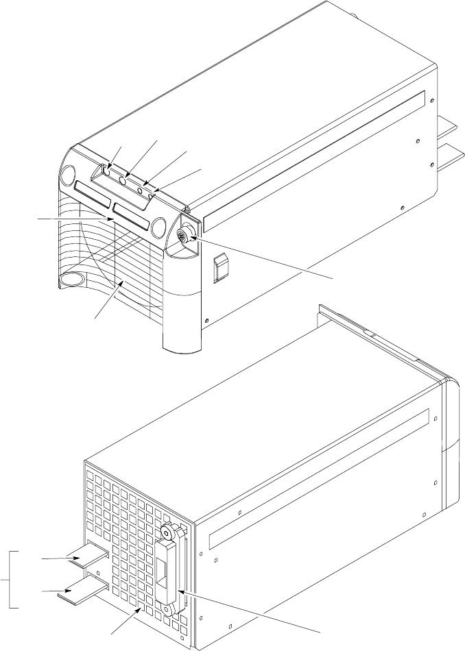
P ower Supply Modules (PSMs) Chapter 10: PSM Shelf R eplacement Procedures
Figure 10 -2 220 V AC PSM Front & R ear Details
ti-cdma-05921.eps
Front
Port (-) Port (+)
Test Test Red
LED
Green
LED
Handle
Air Inlet
Captive M4 Retaining
Thumbscrew
AC Input and
Status/Alarm
Drawer Connector
27V DC
Output
(+)
Feed
(-)
Return
Air Outlet
Rear
10 -22 68P09283A64 -3
FOA SEP 2007
1X UBS Macro B T S FRU P ower Supply Modules (PSMs)
Front Panel LEDs
T wo LEDs are on the front panel of each PSM with the following functionality:
•A GREEN LED is displayed when the PSM is enabled and the output voltage is present.
This LED remains on during a minor alarm condition.
•A RED LED is displayed when a hard failure occurs (for example; a F an failure or Converter
failure).
Front Panel Test Ports
A high impedance DC voltmeter can be connected between the two test ports on the front panel
to monitor the DC output voltage.
Rear Panel Connectors
Blade type contacts, on the rear of the PSM, mate with the DC input/output bus bars at the
rear of the PSM shelf .
The status/alarm drawer connector on the rear of the PSM mates with a bulkhead connector
at the rear of the PSM shelf . This connector is cabled to the PSM alarm connector on the
front of the PSM shelf .
Required items
Documents
•None
Tools
•T orque driver
•T25 TORX driver
Torque requirements
•PSM captive M4 retaining thumbscrew , 2.37 N -m (21 in -lb)
Replacement unit
•–48 V DC P ower Supply Module (–48 V DC PSM) — Motorola model STPN4037
•220 V AC P ower Supply Module (220 V AC PSM) — Motorola model STPN4036
68P09283A64 -3 10 -23
FOA SEP 2007
P ower Supply Modules (PSMs) Chapter 10: PSM Shelf R eplacement Procedures
Prerequisites
Before you begin
Before you begin, record the pertinent information in T able 10 -6 .
Table 10 -6 Item number replacement list
Item
Number
BTS number
F ailed –48 V DC PSM number
F ailed 220 V AC PSM number
PSM replacement procedure
The PSM weighs appro ximately 5 kg. Be careful when handling the PSM to prev ent
damage to the equipment and personal injury .
W earing anti–static wrist str aps during this procedure is not recommended.
Occasionally during this procedure, touch the fr ame ground to dissipate static
electricit y .
P erform the steps described in Procedure 10 -5 to replace either a –48 V DC PSM or a 220 V
AC PSM.
Procedure 10 -5 R eplacing a PSM
1
Notify the OMC–R operator that you are replacing the -48 V DC/220 V AC PSM.
2
It will be helpful if the OMC–R operator executes “ENABLE EVENTS” command at the CLI
session of the OMC–R to monitor alarms. This command is optional and may not be useful if
executed during a high CP U utilization time.
3
Using a T25 TORX bit and driver , loosen the captive retaining thumbscrew until it is
disengaged from the shelf .
Continued
10 -24 68P09283A64 -3
FOA SEP 2007
1X UBS Macro B T S FRU P ower Supply Modules (PSMs)
Procedure 10 -5 R eplacing a PSM (Continued)
4
PSM weighs appro ximately 5 kg. Be careful when handling the PSM to prev ent
damage to the equipment and personal injury .
Grasp the handle on the front panel of the PSM with one hand. Slowly pull the PSM out of
the shelf slot while carefully supporting the bottom of the module with the other hand.
5
Properly orient the replacement PSM and insert it into the slot. Slowly
slide the module into the shelf until the rear connectors are fully seated.
Make sure that the PSM is fully engaged with the shelf backplane slot connectors.
6
Using a T25 TORX bit and torque driver , tighten the captive retaining thumbscrew to 2.37
N-m (21 in-lb).
7
Observe the LEDs on the PSM.
The green LED should be on and the red LED should be off . This indicates normal operation.
There is no optimization required for the PSM replacement.
8
Notify the OMC–R operator that the procedure is complete and that alarms should be cleared.
9
OMC–R operator execute “DISABLE EVENTS” command to discontinue monitoring of alarms.
68P09283A64 -3 10 -25
SEP 2007 FOA
P ower Supply Modules (PSMs) Chapter 10: PSM Shelf R eplacement Procedures
10 -26 68P09283A64 -3
FOA SEP 2007

C h a p t e r
1 1
RX Splitter Replacement Procedure■■■■■■■■■■■■■■■■■■■■■■■■■■■■■■■■■■■■■■■■■■■■■■■■■■■■■■■■■■■■■■
■
■
■
■
68P09283A64 -3 11 -1
SEP 2007 FOA

RX Splitter Chapter 11: RX Splitter R eplacement Procedure
RX Splitter
■■■■■■■■■■■■■■■■■■■■■■■■■■■■■■■■■■■■■■■■■■■■■■■■■■■■■■■■■■■■■■
■
■
RX Splitter Description
The RX splitter is only used in UBS Macro BTS frames equipped with more than one XMI.
The RX splitter used in the UBS Macro BTS frame is wide band and handles either 1.9 GHz or
800 MHz RX signals.
The RX splitter is a passive device requiring no DC input operating power .
F or the RX splitter location in the UBS Macro frame, refer to Figure 1 -3 UBS Macro BTS
mid -capacity frame (1800 mm rack) on page 1 - 30 .
Figure 1 -14 RX splitter front panel detail on page 1 - 44 shows the location of the RX splitter RF
I/O port connectors.
The XMI RX expansion ports (EXP OUT and EXP IN) are connected to the RX splitter .
Currently , UBS Macro BTS frames do not support XMI 3 and XMI 4. These will be
supported in the future.
In frames equipped with an RX splitter , XMI 1 provides RX main RF antenna signal outputs for
each sector to the RX splitter and XMI 2 provides RX diversity RF antenna signal outputs
for each sector to the RX splitter . The RX splitter splits the RX main RF antenna signals into
outputs to XMI 2, XMI 3 and XMI 4. The RX splitter splits the RX diversity RF antenna signals
into outputs to XMI 1, XMI 3 and XMI 4.
The RX splitter XMI 3 and XMI 4 EXP OUT and EXP IN connectors are not currently used.
System impact/considerations
P erforming this replacement procedure will not cause BTS downtime or suspend
any call processing.
Receive diversity on all sectors will be interrupted during the procedure.
TX RF output power on each sector is not affected.
Because the RX splitter is completely passive, the likelihood of its failure is minimal.
11 -2 68P09283A64 -3
FOA SEP 2007

1X UBS Macro B T S FRU RX Splitter
The RX splitter is not redundant.
The following strategy is used during replacement of the RX splitter . When the RX splitter
is disconnected/removed:
•XMI 1 remains connected to the RX main RF antenna signal outputs for each sector , but
has no connection to the RX diversity RF antenna signal outputs for each sector .
•XMI 2 remains connected to the RX diversity RF antenna signal outputs for each sector ,
but has no connection to the RX main RF antenna signal outputs for each sector .
Alarms will be reported during the replacement procedure.
A fter the RX splitter is replaced, all affected RX paths must be tested, and if necessary
reoptimized to ensure accurate RF power levels. Refer to the
1X UBS Macro BTS
Optimization/A TP
manual for test and optimization procedures.
A thorough troubleshooting of the RX antenna paths and all associated XMIs and cables is
required to pinpoint a failure to the RX splitter .
Table 11 -1 FRU R eplacement Conditions
FRU
Ref Designator What to Shut Down...
RX Splitter Not Applicable Nothing
Required Items
Documents
•
1X UBS Macro BTS Optimization/A TP
manual.
Tools
•T25 TORX bit
•T orque driver
Torque Requirements
•M5 mounting screws - 4.77 N -m (42 in -lb)
Replacement Unit
•W ide band (800 MHz through 2.1 GHz RF bands) RX splitter (Motorola model STRG4029)
68P09283A64 -3 11 -3
FOA SEP 2007
RX Splitter Chapter 11: RX Splitter R eplacement Procedure
Prerequisite
Coordinate this repair task with the OMCR operator .
Before you begin
Before you begin, enter the information into the following replacement list table.
Table 11 -2 Item Number R eplacement List
Item
Number
BTS number
F ailed RX splitter number
RX Splitter Replacement Procedure
This procedure requires working on or around circuitry which is extremely sensitiv e to
ESD . W ear a conductiv e, high impedance wrist str ap during the procedure.
Use appropriate safet y measures.
11 -4 68P09283A64 -3
FOA SEP 2007

1X UBS Macro B T S FRU RX Splitter
P erform the steps in Procedure 11 -1 to replace an RX splitter .
Procedure 11 -1 R eplacing an RX Splitter
A T THE BTS SITE
1
W ear a conductive, high impedance wrist strap.
2
Disconnect all cables from the front panel of the RX splitter and move them out of the way .
3
Using a T25 TORX driver , remove the two RX splitter mounting screws; one screw at each of
the end mounting tabs on the front of the module.
4
Carefully remove the RX splitter from the bottom of the XMI shelf .
5
Mount the replacement RX splitter to the bottom of the XMI shelf . Use the two RX splitter
mounting screws; one screw at each of the end mounting tabs on the front of the module.
6
Using a T25 TORX driver , tighten the two RX splitter mounting screws to 4.77 N-m (42 in-lb).
7
Reconnect all cables to the front panel of the RX splitter .
8
This completes the physical installation of the FRU . If optimization is to be performed at this
time, see Optimization Required following this table.
Optimization Required
P erform the following BTS Optimization/A TP procedures:
•RS SI T est (FER T est is optional)
Refer to the
1X UBS Macro BTS Optimization/A TP
manual for the optimization procedures.
68P09283A64 -3 11 -5
SEP 2007 FOA
RX Splitter Chapter 11: RX Splitter R eplacement Procedure
11 -6 68P09283A64 -3
FOA SEP 2007

C h a p t e r
1 2
RGPS Head Replacement Procedure■■■■■■■■■■■■■■■■■■■■■■■■■■■■■■■■■■■■■■■■■■■■■■■■■■■■■■■■■■■■■■
■
■
■
■
68P09283A64 -3 12 -1
SEP 2007 FOA
RGPS (R emote GPS) Head Chapter 12: RGPS Head R eplacement Procedure
RGPS (Remote GPS) Head■■■■■■■■■■■■■■■■■■■■■■■■■■■■■■■■■■■■■■■■■■■■■■■■■■■■■■■■■■■■■■
■
■
RGPS Head Description
The optional RGPS head is remotely located from the UBS Macro BTS frame. The RGPS head
is typically mounted outside on a mast/pole. (See Figure 1 -18 RGPS Head Mounting Details
on page 1 - 50 .)
The RGPS head contains a GPS Receiver (GPSR) and built -in GPS RF antenna.
The RGPS head 12–pin Deutsch type MMP connector is cabled to the S SI RGPS connector . This
connection allows the S SI to supply DC power to the RGPS head. In addition, control/data
signals are exchanged between the UBS Macro BTS frame and RGPS head via this connection.
The RGPS head successfully tracks and acquires GPS satellites. The RGPS head detects GPS
RF signals and extracts a 1 Pulse P er Second (1PPS) timing signal. This 1PPS signal is applied
to the DMI controller via the S SI connector . The DMI controller contains an internal Medium
Stability Oscillator (MSO) that is synchronized to the 1PPS timing signal and locked to the GPS
time base. If satellite tracking is lost or if the RGPS head fails, the MSO can maintain system
timing for up to 8 hours.
If the UBS Macro BTS frame is equipped with an optional Quartz High Stability Oscillator
(QHSO) that is mounted to the rear of the S SI, the DMI controller selects the QHSO as the
backup synchronization source instead of the MSO . The QHSO can maintain system timing
for up to 24 hours.
Motorola RGPS Heads
Currently there are two Motorola RGPS heads that may be used with UBS Macro BTS equipment
(see Figure 1 -19 RGPS Head Equipment on page 1 - 51 ). These are as follows:
•A later version Motorola RGPS head is typically installed at a new UBS Macro BTS site.
•An earlier version Motorola RGPS head already installed at and existing Motorola equipped
BTS site that is being upgraded with UBS Macro BTS equipment.
The installed RGPS cabling supports operation of either version RGPS head. However , the later
version RGPS head requires that the cabling to the head be routed outside the RGPS mounting
mast/pole while the earlier version RGPS head requires that the cabling to the head be routed
through the RGPS mounting mast/pole.
12 -2 68P09283A64 -3
FOA SEP 2007

1X UBS Macro B T S FRU RGPS (R emote GPS) Head
System Impact/Considerations
P erforming this replacement procedure should not require BTS downtime or impact
call processing because of MSO or QHSO backup. However RGPS head downtime
will occur . And alarms will be reported.
A failed RGPS head should be replaced immediately after failure detection and
within the applicable MSO/QHSO backup time period (i.e., up to 8 hours MSO and
up to 24 hours QHSO).
A fter the replacement RGPS head is re -connected and powered up, it may take up to
30 minutes for the replacement RGPS head to successfully track and acquire satellites.
Table 12 -1 FRU R eplacement Conditions
FRU
Ref Designator What to Shut Down...
RGPS head
RGPS
Nothing; FRU is hot swappable and BTS
system timing is backed up by either MSO
(for up to 8 hours) or QHSO (for up to 24
hours).
Required Items
Documents
•
1X UBS Macro BTS Optimization/A TP
manual.
Tools
•Adjustable wrench
68P09283A64 -3 12 -3
FOA SEP 2007

RGPS (R emote GPS) Head Chapter 12: RGPS Head R eplacement Procedure
Replacement Unit
•RGPS Head (Motorola model SLN6594), later version
•RGPS Head (Motorola part number 0186012H04), earlier version
If you need to replace the mounting hardware and/or the cable assembly with the RGPS head,
contact your Motorola sales representative for the appropriate kits.
Prerequisite
Coordinate this repair task with the OMCR operator .
Before You Begin
Before you begin, record the pertinent information in the following table (see T able 12 -2 ):
Table 12 -2 Item Number R eplacement List
Item
Number
BTS number
F ailed RGPS Head number
Replacement RGPS Head
number
RGPS head Replacement Procedure
P erform the steps in Procedure 12 -1 to replace the RGPS Head.
Procedure 12 -1 RGPS Head R eplacement Procedure
A T THE BTS SITE
1
Notify the OMCR operator that you are starting the replacement procedure and that
associated alarm reports can be expected.
2
•F or removal of the earlier RGPS head (Motorola part number 0186012H04), go to step
step 3 .
•F or removal of the later RGPS head (Motorola model SLN6594), go to step step 12 .
Continued
12 -4 68P09283A64 -3
FOA SEP 2007

1X UBS Macro B T S FRU RGPS (R emote GPS) Head
Procedure 12 -1 RGPS Head R eplacement Procedure (Continued)
3
Create slack in the RGPS cable so that 2 feet of cable can be extended out of the RGPS head
end of the mounting pipe/conduit.
4
Loosen the pipe/conduit mounting hardware until the pipe/conduit is free to be unscrewed
from the RGPS head.
5
T o prevent twisting of cables, do not turn the RGPS head while holding the
pipe/conduit.
Grasp the RGPS head with one hand and the pipe/conduit with the other hand.
While holding the head still, unscrew the pipe/conduit from
the head and separate the head from the pipe/conduit.
Grasp the cable just below the head and pull about 16 inches of cable out of the pipe/conduit
until the mating cable connectors are exposed.
6
Separate the mating cable connectors to disconnect the RGPS head from the RGPS cable.
The UBS Macro BTS frame automatically switches over to the backup reference
source, QHSO/MSO , after disconnecting a working RGPS head. Alarm/event
messages are also triggered.
7
Connect the cable connector of the replacement RGPS head to the RGPS cable connector .
Secure the connection by tightening the spinning connector flange.
A fter connecting the replacement head, the UBS Macro BTS frame automatically
switches over to the primary reference source, Remote GPS .
8
F eed the cable slack into the RGPS head end of the mounting pipe/conduit.
9
T o prevent twisting of cables, do not turn the RGPS head while holding the
pipe/conduit.
Grasp the RGPS head with one hand and the pipe/conduit with the other hand.
Being careful not cross-thread the fitting on the RGPS head, screw the pipe/conduit into the
head. Hand tighten only!
10
Tighten the pipe/conduit mounting hardware until the pipe/conduit is securely mounted.
Continued
68P09283A64 -3 12 -5
FOA SEP 2007

RGPS (R emote GPS) Head Chapter 12: RGPS Head R eplacement Procedure
Procedure 12 -1 RGPS Head R eplacement Procedure (Continued)
11 Go to step step 16
12
Disconnect the RGPS cable from the RGPS head connector . It may be helpful to create some
slack in the RGPS cable.
The UBS Macro BTS frame automatically switches over to the backup reference
source, QHSO/MSO , after disconnecting a working RGPS head. Alarm/event
messages are also triggered.
13
Remove the RGPS head by grasping the head and unscrewing it from the mounting
pipe/conduit.
Turn the RGPS head Counter-Clockwise (CCW), as viewed from the top of the
head, to loosen/unscrew .
14
Screw the replacement RGPS head onto the mounting pipe/conduit. Securely tighten the
head.
15
Connect the RGPS cable connector to the replacement RGPS head connector . Secure the
connection by tightening the spinning connector flange.
A fter connecting the replacement head, the UBS Macro BTS frame automatically
switches over to the primary reference source, Remote GPS .
16
A fter the replacement RGPS head is re-connected and powered up, it may take up
to 30 minutes for the replacement RGPS head to successfully track and acquire
satellites.
Notify the OMCR operator that you have completed the replacement procedure.
A T THE OMCR
17
V erify that old alarms are cleared and no new alarms are reported.
18
If optimization is to be performed at this time, see Optimization Required
following this table.
12 -6 68P09283A64 -3
FOA SEP 2007
1X UBS Macro B T S FRU RGPS (R emote GPS) Head
Optimization Required
Consult the
1X UBS Macro BTS Optimization/A TP
manual for the following optimization/test
instructions:
•Timing Initialization/V erification
68P09283A64 -3 12 -7
FOA SEP 2007

Standard Printing Instructions
Part Number 68P09283A64-3
Manual T itle
1X UBS Macro BTS FRU
Date
SEP 2007
CSD/CND (US)
Binder
- 3 Slant D-ring binder - letter size 1 1.75in x 1 1.5in) white PVC.
- Capacity depends on size of document. (no larger than 3 in)
- Clear pockets on front and spine
Printing
- Cover / spine text overprinted onto Motorola cover stock.
- Body printed double sided onto white letter size (8.5in x 1 1in) 70lb.
Finishing
- Shrink wrap contents.
FOA SEP 2007
Barcode
68P09283A64 68P09283A64
68P09283A64
-3 -3
-3
SEP 2007 FOA