Nokia Solutions and Networks T5JX1 UBS CDMA XMI Transceiver at 800 MHz User Manual Exhibit 8f
Nokia Solutions and Networks UBS CDMA XMI Transceiver at 800 MHz Exhibit 8f
Contents
Exhibit 8f

Individual T ests Chapter 4: Acceptance T est Procedures
Receive Signal Strength Indication (RSSI)
This test verifies the gain for UBS reverse (RX) paths for each carrier -sector selected is within
requirements for correct operation for the operating band of the UBS as follows:
•1900 MHz: –80 dBm ( -86 dBm or greater)
•800 MHz: –80 dBm ( -86 dBm or greater)
The LMF injects a -80 dBm signal (default) input to the UBS . The RS SI must be
+/ -6 dB.
4 -16 68P09283A63 -5
FOA A UG 2007
1X UBS Macro B T S Optimization/A TP TX Spectr al Purit y T r ansmit Mask Acceptance T est
TX Spectral Purity Transmit Mask Acceptance Test■■■■■■■■■■■■■■■■■■■■■■■■■■■■■■■■■■■■■■■■■■■■■■■■■■■■■■■■■■■■■■
■
■
TX Mask Test
This test verifies the spectral purity of each sector -carrier at a specific frequency ,
per the
current NEC file assignment
. All tests are performed using the external calibrated test set,
controlled by the same command. All measurements are via the appropriate TX OUT connector .
The standard pattern is used (pilot 171 and 43dBm)
The parameters of the TX Mask are as follows:
> -45.0 dBc / 30 kHz@>750 kHz offset
> -60.0 dBc / 30 kHz@ 1.98 MHz offset
The sector -carrier is keyed or dekeyed during the test.
Figure 4 -3 TX Mask V erication Spectrum Analyz er Displa y (1900 MHz)
ti-cdma-00150-A.eps
- 900 kHz
Center Frequency
Reference
Attenuation level of all
spurious and IM products
with respect to the mean
power of the CDMA channel
.5 MHz Span/Div
Ampl 10 dB/Div
Mean CDMA Bandwidth
Power Reference
+750 kHz- 750 kHz
- 1.98 MHz
+1.98 MHz
68P09283A63 -5 4 -17
FOA A UG 2007
TX W a v eform Qualit y (Rho) Acceptance T est Chapter 4: Acceptance T est Procedures
TX Waveform Quality (Rho) Acceptance Test■■■■■■■■■■■■■■■■■■■■■■■■■■■■■■■■■■■■■■■■■■■■■■■■■■■■■■■■■■■■■■
■
■
Rho Test
The Pilot Gain is set to 171 for each antenna. The sector -carrier is enabled using both rflvl and
bay level offsets, to generate a CDMA carrier (with pilot channel element only , W alsh code 0).
Sector -carrier power output is set to 36 dBm as measured at the TX OUT connector (on the
UBS directional coupler).
The calibrated communications test set measures and returns the Pilot channel element digital
waveform quality (rho) in dB, verifying that the result meets system tolerances:
•W aveform quality (rho) should be greater than or equal to 0.97 ( -0.4 dB).
Figure 4 -4 Rho Signal
ti-cdma-rho_p to.eps
4 -18 68P09283A63 -5
FOA A UG 2007
1X UBS Macro B T S Optimization/A TP TX Pilot Time Offset Acceptance T est
TX Pilot Time Offset Acceptance Test■■■■■■■■■■■■■■■■■■■■■■■■■■■■■■■■■■■■■■■■■■■■■■■■■■■■■■■■■■■■■■
■
■
PTO Acceptance Test
This test verifies the transmitted Pilot channel element Pilot Time Offset of each sector -carrier
keyed up at a specific frequency
per the current NEC file assignment
. All tests are performed
using the external calibrated test set controlled by the same command. All measurements
are via the appropriate TX OUT connector .
The Pilot Gain is set to 171 LSB for each antenna. The sector -carrier is enabled, using both
rfLvl and bay level offsets, to generate a CDMA carrier (with pilot channel element only , W alsh
code 0). Sector -carrier power output is set to 36 dBm as measured at the TX OUT connector
(on the UBS directional coupler).
The calibrated communications test set measures and returns the Pilot Time Offset in us,
verifying results meet system tolerances:
•Pilot Time Offset should be within +/– 3 us of the target PT Offset (0 us).
68P09283A63 -5 4 -19
FOA A UG 2007
TX Pilot Time Offset Acceptance T est Chapter 4: Acceptance T est Procedures
Figure 4 -5 Pilot Only Signal
ti-cdma-pilot_only.eps
4 -20 68P09283A63 -5
FOA A UG 2007

1X UBS Macro B T S Optimization/A TP TX Code Domain P ower/Noise Floor Acceptance T est
TX Code Domain Power/Noise Floor Acceptance Test■■■■■■■■■■■■■■■■■■■■■■■■■■■■■■■■■■■■■■■■■■■■■■■■■■■■■■■■■■■■■■
■
■
Code Domain Power Test
F or each sector/antenna under test, the Pilot Gain is set to 383 LSB. All channel elements under
test are configured to generate Orthogonal Channel Noise Source (OCNS) on standard pattern -
only 9 channels where the 6 Traffic channels (TCH) can be anywhere across the code domain
The maximum number of channel elements (CEs) to be tested at any one time is 32 (32 odd
W alsh codes). If more than 32 CEs exist, then multiple sets of measurements are made; so all
channel elements are verified on all sectors.
Sector -carrier power output is set to 43 dBm as measured at the TX OUT connector .
•CD_PILOT_RA TIO: -6.5dB to -7.5dB
•CD_P AGING_RA TIO: -6.8dB to -7.8dB
•CD_SYNC_RA TIO: -12.8dB to -13.8dB
•CD_TRAFFIC_ON_MAX_RA TIO: -9.8dB to -10.8dB
•CD_TRAFFIC_ON_MIN_RA TIO: -9.8dB to -10.8dB
•CD_TRAFFIC_OFF_MAX_RA TIO: -27dB (none)
Refer to Figure 4 -6 .
If using Advantest test equipment, Code Domain T est MUST be configured in RC -1
mode.
See Procedure 4 -5 to perform this test.
68P09283A63 -5 4 -21
FOA A UG 2007
TX Code Domain P ower/Noise Floor Acceptance T est Chapter 4: Acceptance T est Procedures
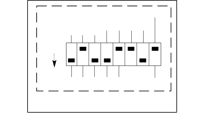
Figure 4 -6 Code Domain P ower and Noise Floor Lev els
ti-cdma-standa rd_pa ttern.eps
PILOT PAGING SYNC TRAFFIC
TRAFFIC
4 -22 68P09283A63 -5
FOA A UG 2007
1X UBS Macro B T S Optimization/A TP RX Fr ame Error R ate (FER) Acceptance T est
RX Frame Error Rate (FER) Acceptance Test■■■■■■■■■■■■■■■■■■■■■■■■■■■■■■■■■■■■■■■■■■■■■■■■■■■■■■■■■■■■■■
■
■
FER Test
This test verifies the UBS FER on all traffic channel elements is currently configured (full
rate at 1% FER) at an RF input level of -123 dBm. All tests are performed using the external
calibrated test set as the signal source controlled by the same command. All measurements
are via the LMF .
The sector -carrier is enabled, using only rflvl level offsets, to generate a CDMA carrier (with
pilot channel element only). Sector -carrier power output is set to +27.5 dBm as measured at the
TX OUT connector . The UBS must be keyed to enable the RX receive circuitry .
The LMF prompts the CE under test to measure all zero long code and provide the FER report
on the selected reverse link for both the main and diversity RX antenna paths, verifying that
results meet the following specification:
•FER returned <1% @ –123 dBm and total frames measured is 1500
All CEs selected are tested on the specified RX antenna path. See Procedure 4 -6 to perform
this test.
68P09283A63 -5 4 -23
FOA A UG 2007
Continuous W a v eform Mode Chapter 4: Acceptance T est Procedures
Continuous Waveform Mode■■■■■■■■■■■■■■■■■■■■■■■■■■■■■■■■■■■■■■■■■■■■■■■■■■■■■■■■■■■■■■
■
■
Objective
This test verifies that the UBS frames can generate an unmodulated carrier tone on a single
sector at any single channel number within the supported carrier frequency range of the frame.
Unlock Continuous Waveform Mode
W inLMF must be connected to the UBS frame to be tested and logged in.
Procedure 4 -7 Procedure to Unlock Continuous W a v eform Mode
1
On the menu, click on UBS -> Unlock Continuous W aveform Mode
2
Click the Y es button in the confirmation dialog box.
3
A status report window will appear that shows the result of the action request.
WinLMF will fail to set up Continuous W a v eform Mode for Modem
devices pro visioned in the congur ation les on DMI, but not
ph ysically installed in the fr ame, and for Modem devices under reset.
4
Select tested Sector/Carrier and click Device->X CVR->K ey menu item.
5
In K ey window:
Enter the desired power level [dBm] in the X CVR Gain box
Enter the desired channel in the X CVR Channel box
6
Click the OK button in K ey window .
A status report window will appear that shows the result of the action request.
7
P erform the required testing on the selected Sector/Carrier .
8
Select Sector/Carrier keyed in step 4 and
click Device->X CVR->Dekey menu item.
A status report window will appear that shows the result of the action request.
9
T o perform unmodulated carrier mode test on
other Sector/Carrier repeat procedure from step 4 .
If testing using unmodulated carrier mode is completed follow Lock
Continuous W aveform Mode Procedure
4 -24 68P09283A63 -5
FOA A UG 2007
1X UBS Macro B T S Optimization/A TP Continuous W a v eform Mode
Lock Continuous Waveform Mode
Procedure 4 -8 Procedure to Lock Continuous W a v eform Mode
1
On the menu, click on UBS -> Lock Continuous W aveform Mode
2
A status report window will appear that shows the result of the action request.
WinLMF will fail to disable Continuous W a v eform Mode for Modem
devices pro visioned in the congur ation les on DMI, but not
ph ysically installed in the fr ame and for Modem devices under reset.
68P09283A63 -5 4 -25
FOA A UG 2007

Gener ate A TP R eport Chapter 4: Acceptance T est Procedures
Generate ATP Report■■■■■■■■■■■■■■■■■■■■■■■■■■■■■■■■■■■■■■■■■■■■■■■■■■■■■■■■■■■■■■
■
■
Background
Each time an Acceptance T est Procedure (A TP) report is updated to include the results of the
most recent A TP tests if the Save Results button is used to close the status report window . The
A TP report
is not
updated if the status reports window is closed using the Dismiss button.
The A TP report for a UBS will contain test results saved with Save Results button.
Results will be saved for the last test performed on the same:
•Sector
•Carrier
•Channel
When an A TP report for a UBS is generated,
all
saved test results will be included
in the report.
ATP Report
Each time an A TP test is run, a report may be created for the UBS being tested. If a previous
report exists for the UBS , it is updated with the new test results as noted above. The report
includes the following for each test:
•T est name
•Channel number
•Carrier number
•Sector number
•T est result
•P AS S or F AIL
•Description information
•Time stamp
•Details/W arning information (if applicable)
The report can be printed if the LMF computer is connected to a printer . F ollow the procedure
in Procedure 4 -9 to view and/or print the A TP report for a UBS .
4 -26 68P09283A63 -5
FOA A UG 2007

1X UBS Macro B T S Optimization/A TP Gener ate A TP R eport
Procedure 4 -9 Gener ating an A TP R eport
1
Click Util .
Save T est Report from the LMF menu.
2
Click on a column heading to sort the report.
3
Do
one
of the following:
•If a printable file copy
is not
desired, click on the Dismiss button.
•If a printable copy
is
required, select the desired file type in the pick
list and click on the Save button.
68P09283A63 -5 4 -27
A UG 2007 FOA
Gener ate A TP R eport Chapter 4: Acceptance T est Procedures
4 -28 68P09283A63 -5
FOA A UG 2007

C h a p t e r
5
Leave the Site■■■■■■■■■■■■■■■■■■■■■■■■■■■■■■■■■■■■■■■■■■■■■■■■■■■■■■■■■■■■■■
■
■
■
■
68P09283A63 -5 5 -1
A UG 2007 FOA

Conguring Backhaul Chapter 5: Lea v e the Site
Conguring Backhaul■■■■■■■■■■■■■■■■■■■■■■■■■■■■■■■■■■■■■■■■■■■■■■■■■■■■■■■■■■■■■■
■
■
Before disconnecting the LMF and test equipment, the span backhaul must be configured to
allow the UBS to communicate with the OMC -R.
Introduction
General
This section allows the Cellular Field Engineers (CFEs) to pre -configure the UBS backhaul
parameters prior to cutting over the UBS . It also contains information on how to make
adjustments to individual backhaul parameters.
Conguring the UBS Backhaul
Prior to BTS cutover , some span configuration and connection parameters must be set to match
the type of backhaul chosen for the particular BTS . These parameters can be checked and
changed if required using the LMF Configure Backhaul Basic Screen. W ith these values set
correctly , the OMC -R should be able to establish communications with the BTS . In the event
that communication between the OMC -R and the BTS is lost and cannot be re -established, the
LMF Configure Backhaul Advanced Screen can be used to restore the backhaul configuration
to default values. See Figure 5 -1 .
The default mode is Full Configuration Backhaul unless the Fractional Span box is
checked.
Backhaul Conguration Procedure
Prior to executing Procedure 5 -1 , the information determined and gathered while working
through the System Engineering Section of the UBS Set -up Procedure should be available. This
information documents the intended backhaul configuration for the site and should match the
configuration the OMC -R is expecting to use for the UBS .
F ailure to congure the UBS backhaul correctly with the LMF using the same DS0
congur ation ma y result in the OMC -R being unable to establish communication with
the UBS at cuto v er .
5 -2 68P09283A63 -5
FOA A UG 2007
1X UBS Macro B T S Optimization/A TP Conguring Backhaul
Figure 5 -1 Congure Backhaul Basic Screen
ti-cdma-06184.eps
Procedure 5 -1 Fr actional Span Backhaul Congur ation Procedure
1
Go to the LMF Configure Backhaul Screen. See Figure 5-1
The default value for both the
LcpNcpNegRetryInt
and the
PPPK eepAliveMsg
parameters is 1000 ms. If the UBS will use
satellite backhaul, the value for these parameters must be set to
2000 ms.
2
If the UBS will use Fractional Span backhaul, click on the F ractional Span box.
The Start DS0 and End DS0 boxes will now accept operator - entered values.
3
Enter the starting DS0 and ending DS0 intended for Span 1 into the
appropriate boxes. The LMF will configure Span 1, which is sufficient to
allow the cutover to succeed. Span 2 will be configured from the OMC-R
after cutover .
4
Select the correct span type, frame type, coding type and span equalization
from the pull-down menus in the Span Configuration section.
5
Click on the OK button.
68P09283A63 -5 5 -3
FOA A UG 2007
Conguring Backhaul Chapter 5: Lea v e the Site
Using the LMF Congure Backhaul Advanced Screen
In the event that a backhaul configuration entered at the Operation and maintenance
Center -R adio (OMC -R) results in the OMC -R being unable to communicate with the BTS , it may
be necessary to reset backhaul parameters to their default values using the LMF . The LMF
Configure Backhaul Advanced Screen is used to reset these values.
Prior to executing Procedure 5 -2 , the information determined and gathered while working
through the System Engineering Section of the BTS Set -up Procedure should be available. This
information documents the intended backhaul configuration for the site and should match the
configuration the OMC -R is expecting to use for the BTS . Default values for those parameters
not covered above are listed below:
•Muxing: enabled
•Header Compression: enabled
•Max Transport Unit Size (bytes): 512
•Hello Interval Timer (seconds): 30
•P eriodic Transmission intervals for join/prune messages (seconds): 60
Connection Configuration (ubsCon)
•Interval between LCP/IPCP retries during PPP link negotiation (milliseconds): 1000
F or satellite backhaul: 2000
•Time between PPP keep -alive messages (milliseconds) 1000
F or satellite backhaul: 2000
•Number of PPP keep -alive messages that can be lost before link is marked down: 5
•Number of retries for LCP/IPCP negotiations: 10
•Fractional Span backhaul: P er SE config
5 -4 68P09283A63 -5
FOA A UG 2007

1X UBS Macro B T S Optimization/A TP Conguring Backhaul
Span configuration (ubsSpan)
•Span type: T1
•Frame type: ESF , Extended ...
•Coding type: B8ZS , Bipolar 8–...
•T ermination type: TX131, 131 to 2...
•Link alarm set threshold (bit errors / second): 30
•Link alarm set duration (seconds): 10
•Link alarm clear threshold (bit errors / second): 30
•Link alarm clear duration (seconds): 10
•Link removal threshold (bit errors / second): 75
•Link removal duration (seconds): 10
•Link recovery threshold (bit errors / second): 75
•Link recovery duration (seconds): 10
Procedure 5 -2 R esetting Backhaul P ar ameters to their Default V alues
1
Go to the LMF Configure Backhaul Screen.
2
Click on the Show Advanced box at the bottom of the screen. A full list of
backhaul parameters will now be displayed. See Figure 5-2
3
Change the values in the entry boxes to align with the default values noted
above.
4
Click on the OK button.
68P09283A63 -5 5 -5
FOA A UG 2007
Conguring Backhaul Chapter 5: Lea v e the Site
Figure 5 -2 Congure Backhaul Adv anced Screen
en ter_filena me_her e_and_mo ve_per_st ep_8
5 -6 68P09283A63 -5
FOA A UG 2007
1X UBS Macro B T S Optimization/A TP Prepare to Lea v e the Site
Prepare to Leave the Site■■■■■■■■■■■■■■■■■■■■■■■■■■■■■■■■■■■■■■■■■■■■■■■■■■■■■■■■■■■■■■
■
■
External Test Equipment Removal
P erform the procedure in Procedure 5 -3 to disconnect the test equipment and configure the
UBS for active service.
Procedure 5 -3 External T est Equipment R emo v al Procedure
1
Disconnect all external test equipment from all TX and RX connectors on
the UBS .
2
Reconnect and visually inspect all TX and RX antenna feed lines on the UBS .
V erif y that all sector antenna feed lines are connected to the correct ports on the
fr ame. Crossed antenna cables will cause system degr adation of call processing.
LMF Removal
Before removing the LMF , verify that the UBS code load is synched with the code load in the
OMC -R.
DO NOT power down the LMF without performing the procedure below .
Corrupted/lost data files may result, and in some cases, the LMF may lock up
F ollow the procedure in Procedure 5 -4 to terminate the LMF session and remove the terminal.
Continued
68P09283A63 -5 5 -7
FOA A UG 2007

Prepare to Lea v e the Site Chapter 5: Lea v e the Site
Procedure 5 -4 LMF T ermination and R emo v al Procedure
1
From the Local T erminal window select File > Exit .
Anytime the LMF is exited from the UBS , the DMI controller(s)
will automatically reboot within 1 minute in order to clear out any
test configurations and boot up under the original configuration in
the NECB and NECJ files.
2
From the W indows T ask Bar click Start > Shutdown .
Click Y es when the Shut Down W indows message appears.
3
Disconnect the LMF terminal Ethernet connector from the UBS cabinet.
4
Disconnect the LMF serial port, the RS -232 to GPIB interface box, and the
GPIB cables as required for equipment transport.
Reset All Devices and Initialize Site Remotely
Devices in the UBS should not be left with data and code loaded from the LMF . The configuration
data and code loads used for normal operation could be different from those stored in the LMF
files. P erform the procedure in Procedure 5 -5 to reset all devices and initialize site remotely .
Procedure 5 -5 R eset UBS Devices and R emote Site Initialization
1
T erminate the LMF session by following the procedure in Procedure 5-4
2
V erify that the OMC-R operator has re-activated the spans.
3
V erify at the OMC-R that the UBS has been integrated and has synchronized
its code and data.
4
Account for all tools used and all parts removed.
5
V isually inspect the UBS for any foreign objects and remove them.
6
V isually inspect all cable connections, ensuring that they are connected as
required for normal UBS operation.
7
V erify no alarm conditions are being reported to the OMC-R.
8
A fter all activities at the site have been completed, contact the OMC-R and
confirm that the UBS is under OMC-R control.
5 -8 68P09283A63 -5
FOA A UG 2007

A p p e n d i x
A
Data Sheets
68P09283A63 -5 A -1
A UG 2007 FOA

Optimization/A TP Checklist Appendix A: Data Sheets
Optimization/ATP Checklist■■■■■■■■■■■■■■■■■■■■■■■■■■■■■■■■■■■■■■■■■■■■■■■■■■■■■■■■■■■■■■
■
■
Verication of Test Equipment Used
Table A -1 T est Equipment Used Checklist
Manufacturer
Model
Serial Number
A -2 68P09283A63 -5
FOA A UG 2007

1X UBS Macro B T S Optimization/A TP Optimization/A TP Checklist
Checklist
Table A -2 Procedure Checklist
Parameter
Specication Comments
P ower Up Procedures
Pre-P ower Up T est
P er Procedure 2-1
Initial P ower Up T est P er Procedure 2-2
and Procedure 2-3
Optimization/A TP Procedures
LMF -to-UBS
Connection
P er Procedure 3-2
UBS GUI Login
P er Procedure 3-3
UBS GUI Logout
P er Procedure 3-4
Generate A TP Report
P er Procedure 4-9
Leave the Site
T est Equipment
Removal
P er Procedure 5-3 ,
Procedure 5-5
Reset Devices and
Initialize Site Remotely
P er Procedure 5-5
68P09283A63 -5 A -3
A UG 2007 FOA
A -4 68P09283A63 -5
FOA A UG 2007

A p p e n d i x
B
FRU Optimization/ATP Matrix
68P09283A63 -5 B -1
A UG 2007 FOA

FRU Optimization/A TP T est Matrix Appendix B: FRU Optimization/A TP Matrix
FRU Optimization/ATP Test Matrix■■■■■■■■■■■■■■■■■■■■■■■■■■■■■■■■■■■■■■■■■■■■■■■■■■■■■■■■■■■■■■
■
■
Usage & Background
Re -optimization of specific portions of the site may be required. An outline of some basic
guidelines is included in the following tables.
Re -optimization steps listed for any assembly detailed in the tables below must be
performed anytime an RF cable associated with it is replaced.
UBS Optimization Required
Table B -1 When Optimization is R equired
Item Replaced
Optimize
XMI, IDRF , DMI, S SI, CRMS
All sector / carrier TX / RX paths
Detailed Reduced ATP
There Reduced A TP consists of the TX Audit and RS SI tests.
Detailed Optional Full ATP Test Matrix
T able B -2 outlines the optional A TP tests that would need to be performed if the user wants to
fully test the UBS components or if the reduced A TP fails. It is also assumed that all modules
are placed in a Locked State via the LMF .
The following guidelines should also be noted when using this table.
B -2 68P09283A63 -5
FOA A UG 2007

1X UBS Macro B T S Optimization/A TP FRU Optimization/A TP T est Matrix
Not every procedure required to bring the site back on line is indicated in T able B -2 .
It is meant to be used as a guideline
ONL Y
. The table assumes that the user is
familiar enough with the UBS Optimization/A TP procedure to understand which test
equipment set ups, test set calibrations, and UBS site preparation will be required
before performing the T able # procedures referenced.
V arious passive UBS components (such as the TX and RX directional couplers, etc.) only call for
a TX or RX calibration audit to be performed in lieu of a full path calibration. If the RX or TX
path calibration audit fails, the entire RF path calibration will need to be repeated. If the RF
path calibration fails, further troubleshooting is warranted.
Whenever any unit is replaced, it is assumed that only power to the unit being replaced is
turned off via the breaker supplying that unit.
Table B -2 Full A TP T est Matrix
T est
Procedure Description
Reference
RX Cables Run the appropriate LMF applications
RS SI T est
FER T est
5
5
TX Cables Run the appropriate LMF application TX Audit
4
GPS
Run the appropriate LMF applications
GPS
Initialization/V erification
TX Audit
RS SI T est
W aveform Quality A TP
Pilot Time Offset A TP
Code Domain
P ower/Noise Floor
FER T est
•
*
6
*
*
6
6
OPTIMIZA TION AND TEST LEGEND
•Required
* P erform if necessary for additional fault isolation, repair assurance, or site certification
1 P erform on all carrier and sector TX paths to the UBS .
2 P erform on all carrier and sector RX paths to the UBS .
3 P erform on all primary and redundant TX paths of the affected carrier .
4 P erform on the affected carrier and sector TX paths.
5 P erform on the affected carrier and sector RX paths.
6 V erify performance by performing on one sector of on carrier only .
68P09283A63 -5 B -3
A UG 2007 FOA
B -4 68P09283A63 -5
FOA A UG 2007

A p p e n d i x
C
CDMA Operating Frequency
68P09283A63 -5 C -1
A UG 2007 FOA

800 MHz CDMA Oper ating Frequency Progr amming Information Appendix C: CDMA Oper ating Frequency
800 MHz CDMA Operating Frequency Programming
Information
■■■■■■■■■■■■■■■■■■■■■■■■■■■■■■■■■■■■■■■■■■■■■■■■■■■■■■■■■■■■■■
■
■
Introduction
Programming of each of the BTS XMIs is performed by the BTS DMI modules over the
Concentration Highway Interface (CHI) bus. This programming data determines the transmit
and receive operating frequencies (channels) for each XMI.
800 MHz Channels
Figure C -1 shows the total channels for the 800 MHz frequency spectrum and the channels
allocated to CDMA. There are 10 CDMA channels used in a CDMA system. The channels used
are unique to each customer system.
T able C -1 shows the channel allocations and frequencies covered by the UBS Macro .
Table C -1 800 MHz Channel Allocations
System
Designator
CDMA Channel V alidity Channel No. RX (MHz) TX (MHz)
A
(see NOTE
below)
Not V alid
Conditionally V alid
V alid
991–1012
1013–1020
1021–1023
824.04–824.67
824.70–824.91
824.94–825.00
869.04–869.67
869.70–869.91
869.94–870.00
A
V alid
Conditionally V alid
Not V alid
1–303
304–311
312–333
825.03–834.09
834.12–834.33
834.36–834.99
870.03–879.09
879.12–879.33
879.36–879.99
B
Not V alid
Conditionally V alid
V alid
Conditionally V alid
Not V alid
334–355
356–363
364–636
637–644
645–666
835.02–835.65
835.68–835.89
835.92–844.32
844.11–844.32
844.35–844.98
880.02–880.65
880.68–880.89
880.92–889.32
889.11–889.32
889.35–889.98
A ’
Not V alid
Conditionally V alid
Not V alid
667–688
689–694
695–716
845.01–845.64
845.67–845.82
845.85–846.48
890.01–890.64
890.67–890.82
890.85–891.48
B’
Not V alid
Conditionally V alid
V alid
Conditionally V alid
Not V alid
717–738
739–746
747–769
770–777
778–799
846.51–847.14
847.17–847.38
847.41–848.07
848.10–848.31
848.34–848.97
891.51–892.14
892.17–892.38
892.41–893.07
893.10–893.31
893.34–893.97
India Conditionally V alid
V alid
1013–1020
1021–594
824.70–824.91
824.94–842.82
869.70–869.91
869.94–887.82
C -2 68P09283A63 -5
FOA A UG 2007

1X UBS Macro B T S Optimization/A TP 800 MHz CDMA Oper ating Frequency Progr amming Information
Table C -1 800 MHz Channel Allocations (Continued)
System
Designator
CDMA Channel V alidity Channel No. RX (MHz) TX (MHz)
China V alid
37–283 826.11–833.49 871.11–878.49
The UBS supports all valid channels within the 800 MHz band and two Conditionally V alid channels: 1019
and 1020. On any other conditionally valid channels within the 800 MHz band, full TX Output power
cannot be supported.
68P09283A63 -5 C -3
A UG 2007 FOA
800 MHz CDMA Oper ating Frequency Progr amming Information Appendix C: CDMA Oper ating Frequency
Figure C -1 800 MHz Frequency Spectrum (CDMA Allocation)
ti-cdma-05810.eps
1
644
(MHz)
F R E Q U E N C Y I N C R E A S E
CHANNELS
824.700
824.910
833.490
844.140
RX TX
825.000
869.700
834.090 879.090
889.320
844.110 889.110
897.330
880.680
637
356
283
303
1013
824.880 869.880 1019
869.910 1020
870.000 1023
825.030 870.030
37825.110 870.110
878.490
835.860
834.120 879.120 304
311
834.330
835.680
880.860 362
363098.088098.538
638
889.140
844.320
847.170
694
689
890.670845.670
845.820 890.820
746
770
739
847.410
847.380
892.170
892.380 747
892.410
848.100 893.100 771
777
848.130 893.130
848.330 893.330
C -4 68P09283A63 -5
FOA A UG 2007

1X UBS Macro B T S Optimization/A TP 800 MHz CDMA Oper ating Frequency Progr amming Information
800 MHz Channel Center Frequencies
T able C -2 shows the valid 800 MHz CDMA channels, listed in both decimal and hexadecimal,
and the corresponding transmit and receive frequency for each.
Actual frequencies used depend on customer CDMA system frequency plan.
Other channels and frequencies can be calculated using the following formula:
F or channels 1–799:
•TX Freq = 870.00 + (0.03 x Channel)
•RX Freq = (0.03 x Channel) + 825.00
F or channels 991–1023:
•TX Freq = 870.00 + [0.03 x (Channel - 1023)]
•RX Freq = [0.030 x (Channel - 1023)] + 825.00
F or channels 1024–1323:
•TX Freq = 860.04 + [0.03 x (Channel - 1024)]
•RX Freq = [0.030 x (Channel - 1024)] + 815.04
F or channels 1324–1490:
•TX Freq = 860.04 + [0.03 x (Channel - 1024)]
•RX Freq = [0.030 x (Channel - 1024)] + 815.04
Table C -2 800 MHz TX and RX Channel Center Frequencies
Decimal Hex
T ransmit Center Frequency (MHz) Receive Center Frequency (MHz)
1021 03FD 869.94 824.94
1023 03FF 870.00 825.00
1 0001 870.03 825.03
303 012F 879.09 834.09
364 016C 880.92 835.92
636 027C 889.32 844.32
666 029A 889.99 844.35
716 02CC 891.49 844.98
747 02EB 893.10 847.71
769 0301 893.31 848.07
68P09283A63 -5 C -5
A UG 2007 FOA

1900 MHz CDMA Oper ating Frequency Progr amming Information Appendix C: CDMA Oper ating Frequency
1900 MHz CDMA Operating Frequency Programming
Information
■■■■■■■■■■■■■■■■■■■■■■■■■■■■■■■■■■■■■■■■■■■■■■■■■■■■■■■■■■■■■■
■
■
Introduction
Programming of each of the BTS XMIs is performed by the BTS DMI modules over the
Concentration Highway Interface (CHI) bus. This programming data determines the transmit
and receive operating frequencies (channels) for each XMI.
1900 MHz Channels
Figure C -2 shows the total channels for the 1900 MHz frequency spectrum and the channels
allocated to CDMA. The channels used are unique to each customer system.
T able C -3 shows the channel allocations and frequencies covered by the UBS Macro .
Table C -3 1900 MHz Band Class 1 Channel Allocations
CDMA Channel V alidity Channel Number TX (MHz) RX (MHz)
Not V alid
0–24 1930.00–1931.20 1850.00–1851.20
V alid
25–1175 1931.25–1988.75 1851.25–1908.75
Not V alid
1176–1199 1988.80–1989.95 1908.80–1909.95
C -6 68P09283A63 -5
FOA A UG 2007

1X UBS Macro B T S Optimization/A TP 1900 MHz CDMA Oper ating Frequency Progr amming Information
Figure C -2 1900 MHz Frequency Spectrum (CDMA Allocation)
ti-cdma-05810-B.eps
450
1100
(MHz)
F R E Q U E N C Y I N C R E A S E
CHANNELS
1851.25
1860.00
RX TX
1867.50
1931.25
1882.50 1962.50
1985.00
1902.50 1982.50
1967.50
1971.25
1050
825
525
650
25
1855.00 1935.00 100
1940.00 200
1947.50 350
1872.50
1956.25
1895.00
750
1887.50
1891.25
1975.00 900
1905.00
1175
1988.751908.75
1952.50
1876.25
68P09283A63 -5 C -7
A UG 2007 FOA

1900 MHz CDMA Oper ating Frequency Progr amming Information Appendix C: CDMA Oper ating Frequency
1900 MHz Channel Center Frequencies
T able C -4 shows some of the valid 1900 MHz CDMA channels, listed in both decimal and
hexadecimal, and the corresponding transmit and receive frequency for each.
Actual frequencies used depend on customer CDMA system frequency plan.
Other channels and frequencies can be calculated using the following formula:
F or channels 0–1199:
•TX Freq = 1930.00 + (0.05 x Channel)
•RX Freq = 1850.00 + (0.05 x Channel)
Table C -4 1900 MHz TX and RX Channel Center Frequencies
Decimal Hex
T ransmit Center Frequency (MHz) Receive Center Frequency (MHz)
25 0019 1931.25 1851.25
100 0064 1935.00 1855.00
200 00C8 1940.00 1860.00
350 015E 1947.50 1867.50
450 01C2 1952.50 1872.50
525 020D 1956.25 1876.25
650 028A 1962.50 1882.50
750 02EE 1967.50 1887.50
825 0339 1971.25 1891.25
900 0384 1975.00 1895.00
1050 041A 1982.50 1902.50
1100 044C 1985.00 1905.00
1175 0497 1988.75 1908.75
C -8 68P09283A63 -5
FOA A UG 2007
1X UBS Macro B T S Optimization/A TP CDMA Oper ating Frequency Progr amming Information
CDMA Operating Frequency Programming Information■■■■■■■■■■■■■■■■■■■■■■■■■■■■■■■■■■■■■■■■■■■■■■■■■■■■■■■■■■■■■■
■
■
Introduction
Programming of each of the BTS XMIs is performed by the BTS GLI cards over the Concentration
Highway Interface (CHI) bus. This programming data determines the transmit and receive
operating frequencies (channels) for each XMI.
68P09283A63 -5 C -9
A UG 2007 FOA

CDMA Oper ating Frequency Progr amming Information Appendix C: CDMA Oper ating Frequency
2100 MHz Channels
Figure C -1 Figure C -3 shows the total channels for the 2100 MHz frequency spectrum and
the channels allocated to CDMA. There are 10 CDMA channels used in a CDMA system. The
channels used are unique to each customer system.
Figure C -3 2100 MHz Frequency Spectrum (CDMA Allocation)
ti-cdma-00115.eps
FREQ (MHz)
RX TX
CHANNEL
1926.25
125
1978.75
2116.25
2168.75
1
C
D
M
A
CDMA2100MHZ-1
1175
1199
C -10 68P09283A63 -5
FOA A UG 2007

1X UBS Macro B T S Optimization/A TP CDMA Oper ating Frequency Progr amming Information
Calculating 2100 MHz Channel Center Frequencies
T able C -5 shows the valid 2100 MHz CDMA channels, listed in both decimal and hexadecimal,
and the corresponding transmit and receive frequencies for each. Center frequencies (in MHz)
for channels not shown in the table may be calculated as follows:
•TX = 2110 + 0.05 * Channel# Example: Channel 262 TX = 2110 + 0.05 * 262 = 2123.10
MHz
•RX = 1920 + 0.05 * Channel# Example: Channel 262 RX = 1920 + 0.05 * 262 = 1933.10
MHz
Actual frequencies used depend on customer CDMA system frequency plan.
Each CDMA channel requires a 1.77 MHz frequency segment. The actual CDMA carrier is 1.23
MHz wide, with a 0.27 MHz guard band on both sides of the carrier .
Minimum frequency separation required between any CDMA carrier and the nearest
NAMPS/AMPS carrier is 900 kHz (center -to -center).
Table C -5 2100 MHz TX and RX Channel Center Frequencies
Channel Number
Decimal
Hex
Transmit Center
Frequency (MHz)
Receive Center
Frequency (MHz)
125 007D 2116.25 1926.25
150 0096 2117.50 1927.50
175 00AF 2118.75 1928.75
200 00C8 2120.00 1930.00
225 00E1 2121.25 1931.25
250 00F A 2122.50 1932.50
275 0113 2123.75 1933.75
300 012C 2125.00 1935.00
325 0145 2126.25 1936.25
350 015E 2127.50 1937.50
375 0177 2128.75 1938.75
400 0190 2130.00 1940.00
425 01A9 2131.25 1941.25
450 01C2 2132.50 1942.50
475 01DB 2133.75 1943.75
500 01F4 2135.00 1945.00
525 020D 2136.25 1946.25
550 0226 2137.50 1947.50
575
023F 2138.75 1948.75
600 0258 2140.00 1950.00
68P09283A63 -5 C -11
A UG 2007 FOA

CDMA Oper ating Frequency Progr amming Information Appendix C: CDMA Oper ating Frequency
Table C -5 2100 MHz TX and RX Channel Center Frequencies (Continued)
Channel Number
Decimal
Hex
Transmit Center
Frequency (MHz)
Receive Center
Frequency (MHz)
625 0271 2141.25 1951.25
650 028A 2142.50 1952.50
675 02A3 2143.75 1953.75
700 02B C 2145.00 1955.00
725 02D5 2146.25 1956.25
750 02EE 2147.50 1957.50
775
0307 2148.75 1958.75
800 0320 2150.00 1960.00
825 0339 2151.25 1961.25
850 0352 2152.50 1962.50
875 036B 2153.75 1963.75
900 0384 2155.00 1965.00
925 039D 2156.25 1966.25
950 03B6 2157.50 1967.50
975 03CF 2158.75 1968.75
1000 03E8 2160.00 1970.00
1025 0401 2161.25 1971.25
1050 041A 2162.50 1972.50
1075 0433 2163.75 1973.75
1100 044C 2165.00 1975.00
1125 0465 2166.25 1976.25
1150 047E 2167.50 1977.50
1175 0497 2168.75 1978.75
C -12 68P09283A63 -5
FOA A UG 2007

A p p e n d i x
D
Test Equipment Preparation
68P09283A63 -5 D -1
A UG 2007 FOA
T est Equipment Prepar ation Appendix D: T est Equipment Prepar ation
Test Equipment Preparation■■■■■■■■■■■■■■■■■■■■■■■■■■■■■■■■■■■■■■■■■■■■■■■■■■■■■■■■■■■■■■
■
■
This section provides pre–testing set–up information for test equipment supported by the LMF .
Purpose
Pretesting set–up information covered includes verification and setting GPIB addresses,
inter–unit cabling, connectivity testing, pre–test control settings, and equipment calibration for
items which are not calibrated with the Calibrate T est Equipment function of the LMF .
GPIB addresses
This appendix provides information on verification and changing GPIB addresses for the
following test equipment items:
•Agilent E7495A/B test equipment set–up
•Agilent E4406A transmitter test set
•Agilent E4432B signal generator
•Advantest R3267 spectrum analyzer
•Advantest R3562 signal generator
•Agilent 8935 analyzer (formerly HP 8935)
•Advantest R3465 analyzer
•Gigatronics 8541C power meter
•Agilent E4418 power meter
•GPIB adapter
Calibration actions
The following calibration–related subjects are also covered for the test equipment items
indicated:
Cable calibration set -up – Calibrating T est Cable Set–up using Advantest R3465
D -2 68P09283A63 -5
FOA A UG 2007
1X UBS Macro B T S Optimization/A TP T est Equipment Prepar ation
Calibrating test sets –
•Agilent E4406A Transmitter T ester Self -alignment (Calibration)
•Gigatronics 8541C power meter (Calibration)
68P09283A63 -5 D -3
A UG 2007 FOA

Agilent E7495A/B T est Equipment Setup Appendix D: T est Equipment Prepar ation
Agilent E7495A/B Test Equipment Setup■■■■■■■■■■■■■■■■■■■■■■■■■■■■■■■■■■■■■■■■■■■■■■■■■■■■■■■■■■■■■■
■
■
Initial Requirement
This test equipment requires a warm -up period of at least 30 minutes before BTS testing or
calibration begins.
Using the Agilent E7495A/B with the LMF
The Agilent E7495A/B does not require the use of the 19MHz frequency reference; if connected,
it will be ignored. The Even Sec SYNC connection is required.
The Agilent E7495A/B signal generator is only calibrated down to -80dB. In order to achieve
accurate FER testing, be sure the RX setup includes at least 40dB of attenuation. This will
ensure the signal generator will output sufficient power to operate in the calibrated range.
Set the IP Address in the test set as described in .
Procedure D -1 Set IP Address on Agilent E7495A/B test set
1
Use the System Button >Controls >IP Admin to set an IP address on the E7495A/B as
128.0.0.11 , and Netmask to 255.255.255.128 .
2
If the IP addressed was changed, reboot the E7495
3
F or compatibility , change the LMF computer Network Interface Card (NIC) IP address to
128.0.0.48, subnetmask 255.255.255.128.
Connection
Connect the E7495A/B test set as described in the Figure 3 -29 T est Equipment Connection to
the LMF .
Power Sensor Calibration
Procedure D -2 describes the E7495A/B P ower Sensor Calibration.
Procedure D -2 E7495A/B P ower Sensor Calibr ation
1
Display the power meter screen.
2
Make sure equipment is connected as shown in Figure D -1 .
D -4 68P09283A63 -5
FOA A UG 2007
1X UBS Macro B T S Optimization/A TP Agilent E7495A/B T est Equipment Setup
Procedure D -2 E7495A/B P ower Sensor Calibr ation (Continued)
3
Zero the power meter by doing the following:
1. Press the Zero softkey .
2. Press the Continue softkey .
4
Calibrate the power meter by doing the following:
1. Press Ref CF .
2. Enter the reference cal factor , reading it off the label on the power sensor head.
3. Press Calibrate .
4. Connect the power sensor (see Figure D -2 ).
5. Press Continue .
6. Press Cal Factor .
7. Enter the cal factor from the label on the power sensor head. Select a cal factor that is
within the operating frequency of the base station being calibrated.
Figure D -1 Agilent E7495A/B Pre -P ower Sensor Calibr ation Connection
ti-cdma-00116.eps
Use only
Agilent supplied
power adapter
GPS
GPIO
Serial 1
Serial 2
Power REF
50 MHz
Sensor
Ext Ref
In
Even Second
Sync In
Antenna
Port 1
RF Out / SWR
Port 2
RF In
POWER SENSOR
NOT CONNECTED
Figure D -2 Agilent E7495A/B P ower Sensor Calibr ation Connection
ti-cdma-00117.eps
Use only
Agilent supplied
power adapter
GPS
GPIO
Serial 1
Serial 2
Power REF
50 MHz
Sensor
Ext Ref
In
Even Second
Sync In
Antenna
Port 1
RF Out / SWR
Port 2
RF In
POWER SENSOR
CONNECTED
68P09283A63 -5 D -5
A UG 2007 FOA
Agilent E7495A/B T est Equipment Setup Appendix D: T est Equipment Prepar ation
Cable Calibration
F ollow the directions in the LMF application program to calibrate cables.
Additional cable calibration details - Calibrate the short cable (see Figure 3 -25 )
and two 10 dB attenuators to establish a baseline and then calibrate the TX and RX set -ups.
Because at least 40 dB of attenuation is needed when testing the FER, the set -up for RX is
the same as for TX.
D -6 68P09283A63 -5
FOA A UG 2007
1X UBS Macro B T S Optimization/A TP V erif ying and Setting GPIB Addresses – Agilent E4406A T r ansmitter T ester
Verifying and Setting GPIB Addresses – Agilent E4406A
Transmitter Tester■■■■■■■■■■■■■■■■■■■■■■■■■■■■■■■■■■■■■■■■■■■■■■■■■■■■■■■■■■■■■■
■
■
Figure D -3 Setting Agilent E4406A GPIB Address
ti-cdma-00118.eps
System Key
Bk Sp Key
Enter Key
Data Entry KeypadSoftkey Buttons
Softkey Label Display AreaActive Function Area
ti-CDMA-WP-00085-v01-ildoc-ftw
Refer to Figure D -3 when performing the following:
Procedure D -3 V erif y and Set/Change Agilent E4406A T r ansmitter T ester GPIB
Address
1
In the SYSTEM section of the instrument front panel, press the System key .
Result: The softkey labels displayed on the right side of the instrument screen will
change.
2
Press the Config I/O softkey button to the right of the instrument screen.
Result:
•The softkey labels will change.
•The current instrument GPIB address will be displayed below the GPIB Address
softkey label.
3
If the current GPIB address is not set to 18 , perform the following to change it:
1. Press the GPIB Address softkey button.
Result: In the on-screen Active F unction Area, GPIB Address will be displayed
followed by the current GPIB address.
68P09283A63 -5 D -7
A UG 2007 FOA

V erif ying and Setting GPIB Addresses – Agilent E4406A T r ansmitter T ester Appendix D: T est Equipment Prepar ation
Procedure D -3 V erif y and Set/Change Agilent E4406A T r ansmitter T ester GPIB
Address (Continued)
2. On the front panel Data Entry keypad, enter the communications system analyzer
GPIB address of 18
Result:
The GPIB Address label will change to Enter .
Digits entered with the keypad will replace the current GPIB address in the
display .
T o correct an entry , press the Bk Sp key at the upper right of the
keypad to delete one character at a time.
3. Press the Enter softkey button or the keypad Enter key to set the new GPIB address.
Result:
The Cong I/O softkey labels will reappear .
The new GPIB address will be displayed under the GPIB Address softkey label.
D -8 68P09283A63 -5
FOA A UG 2007
1X UBS Macro B T S Optimization/A TP V erif ying and Setting GPIB Addresses – Agilent E4432B Signal Gener ator
Verifying and Setting GPIB Addresses – Agilent E4432B
Signal Generator
■■■■■■■■■■■■■■■■■■■■■■■■■■■■■■■■■■■■■■■■■■■■■■■■■■■■■■■■■■■■■■
■
■
Figure D -4 Setting Agilent E4432B GPIB Address
ti-cdma-00119.eps
Numeric
Keypad
Softkey
Buttons
Softkey Label
Display Area
Active Entry
Area
Backspace
Key
Utility Key
ti-CDMA-WP-00086-v01-ildoc-ftw
Refer to Figure D -4 when performing the following:
Procedure D -4 V erif y and Change Agilent E4432B Signal Gener ator GPIB Address
1
In the MENUS section of the instrument front panel, press the Utility key .
Result:
•The softkey labels displayed on the right side of the instrument screen will change.
2
Press the GPIB/RS232 softkey button to the right of the instrument screen.
Result:
•The softkey labels will change.
•The current instrument GPIB address will be displayed below the GPIB Address
softkey label.
3
If the current GPIB address is not set to 1, perform the following to change it:
1. Press the GPIB Address softkey button.
Result:
68P09283A63 -5 D -9
A UG 2007 FOA

V erif ying and Setting GPIB Addresses – Agilent E4432B Signal Gener ator Appendix D: T est Equipment Prepar ation
Procedure D -4 V erif y and Change Agilent E4432B Signal Gener ator GPIB Address
(Continued)
The GPIB Address label and current GPIB address will change to boldface.
In the on-screen Active Entry Area, Address: will be displayed followed by the
current GPIB address.
2. On the front panel Numeric keypad, enter the signal generator GPIB address of 1.
Result:
The GPIB Address label will change to Enter .
Digits entered with the keypad will replace the current GPIB address in the
Active Entry display .
T o correct an entry , press the backspace key at the lower right of the
keypad to delete one character at a time.
3. Press the Enter softkey button to set the new GPIB address.
Result:
The new GPIB address will be displayed under the GPIB Address softkey label.
D -10 68P09283A63 -5
FOA A UG 2007
1X UBS Macro B T S Optimization/A TP V erif ying and Setting GPIB Addresses – Adv antest R3267 Spectrum Analyz er
Verifying and Setting GPIB Addresses – Advantest
R3267 Spectrum Analyzer■■■■■■■■■■■■■■■■■■■■■■■■■■■■■■■■■■■■■■■■■■■■■■■■■■■■■■■■■■■■■■
■
■
Figure D -5 Setting Adv antest R3267 GPIB Address
ti-cdma-00120.eps
onREMOTE LED
LCL Key
CONFIG Key
Softkey Lable
Display Area Softkey
Buttons
Keypad BS Key ENTR Key ti-CDMA-WP-00083-v01-ildoc-ftw
Refer to Figure D -5 when performing the following.
Procedure D -5 V erif y and Set/Change Adv antest R3267 GPIB Address
1
If the REMOTE LED is lighted, press the LCL key .
Result:
•The LED extinguishes.
2
Press the CONFIG key .
Result:
•The CONFIG softkey labels will appear in the softkey label display area of the
instrument display .
•The current GPIB address will be displayed below the GPIB Address softkey label.
3
If the current GPIB address is not set to 18 , perform the following to change it:
1. Press the GPIB Address softkey .
Result: AGPIB Address entry window will open in the instrument display showing the
current GPIB address.
68P09283A63 -5 D -11
A UG 2007 FOA

V erif ying and Setting GPIB Addresses – Adv antest R3267 Spectrum Analyz er Appendix D: T est Equipment Prepar ation
Procedure D -5 V erif y and Set/Change Adv antest R3267 GPIB Address (Continued)
2. Enter 18 on the keypad in the ENTR Y section of the instrument front panel.
T o correct an entry , press the BS (backspace) key at the lower right of the
keypad to delete one character at a time.
Result: Characters typed on the keypad will replace the address displayed in the GPIB
Address entry window .
3. Press the ENTR key to the lower right of the keypad to enter the address.
Result:
The GPIB Address entry window closes.
The new address is displayed in the bottom portion of the GPIB Address
softkey label.
D -12 68P09283A63 -5
FOA A UG 2007
1X UBS Macro B T S Optimization/A TP V erif ying and Setting GPIB Addresses – Adv antest R3562 Signal Gener ator
Verifying and Setting GPIB Addresses – Advantest
R3562 Signal Generator■■■■■■■■■■■■■■■■■■■■■■■■■■■■■■■■■■■■■■■■■■■■■■■■■■■■■■■■■■■■■■
■
■
Set the GP -IB ADDRES S switch on the rear of the Advantest R3562 signal generator to address
1as shown in Figure D -6 .
Figure D -6 Adv antest R3562 GPIB Address S witch Setting
ti-cdma-00121.eps
SERIALI/O
GPIB
CLOCK OUT
12
MAIN
POWER
1
0
SYNTHE
REF
IN 10MHZREF
OUT
ON
OFF
Q
IN/OUT
I
IN/OUT
LOCAL
OUT
GP-IBADDRESSES
54321
1 2 3 4 5 6 7 8
5 4 3 2 1
GP-IP ADDRESS
1
0
GPIB Address set to ?1"
68P09283A63 -5 D -13
A UG 2007 FOA
V erif ying and Setting GPIB Addresses – Agilent 8935 Series E6380 T est Set Appendix D: T est Equipment Prepar ation
Verifying and Setting GPIB Addresses – Agilent 8935
Series E6380 Test Set■■■■■■■■■■■■■■■■■■■■■■■■■■■■■■■■■■■■■■■■■■■■■■■■■■■■■■■■■■■■■■
■
■
Figure D -7 Setting Agilent 8935 T est Set GPIB Address
ti-cdma-00122.eps
FW00885
Preset
Cursor Control
Shift
Inst Config
Local
This procedure assumes that the test equipment is set up and ready for testing.
Refer to Figure D -7 when performing the following.
Procedure D -6 V erif y and Set/Change Agilent 8935 Series E6380 T est Set GPIB
Address
1
The HP I/O configuration MUST be set to T alk & Listen, or NO device on
the GPIB bus will be accessible. (Consult test equipment manufacturer’s
documentation for additional information as required.)
D -14 68P09283A63 -5
FOA A UG 2007

1X UBS Macro B T S Optimization/A TP V erif ying and Setting GPIB Addresses – Agilent 8935 Series E6380 T est Set
Procedure D -6 V erif y and Set/Change Agilent 8935 Series E6380 T est Set GPIB
Address (Continued)
T o verify that the GPIB addresses are set correctly , press Shift and LOCAL on the 8935.
The current HP -IB address is displayed at the top of the screen.
HP -IB is the same as GPIB.
2
If the current GPIB address is not set to 18 , perform the following to change it:
1. Press Shift and Inst Cong .
2. Turn the Cursor Control knob to move the cursor to the HP -IB Adrs field.
3. Press the Cursor Control knob to select the field.
4. Turn the Cursor Control knob as required to change the address to 18.
5. Press the Cursor Control knob to set the address.
3
Press Preset to return to normal operation.
68P09283A63 -5 D -15
A UG 2007 FOA
V erif ying and Setting GPIB Addresses – Gigatronics 8541C P ower Meter Appendix D: T est Equipment Prepar ation
Verifying and Setting GPIB Addresses – Gigatronics
8541C Power Meter■■■■■■■■■■■■■■■■■■■■■■■■■■■■■■■■■■■■■■■■■■■■■■■■■■■■■■■■■■■■■■
■
■
Figure D -8 Gigatronics 8541C P ower Meter Detail
ti-cdma-00128.eps
CONNECT POWER SENSOR
WITH POWER METER
TURNED OFF
CONNECT POWER SENSOR TO
CALIBRATOR POWER REFERENCE
WHEN CALIBRATING/ZEROING UNIT
CALIBRATOR
ZERO
CAL FREQREL
MENU
ESCAPE
dB/MWRECALL
LOCAL
ENTER
A
MODE
GPIBPOWER
I
O
Giga-tronics8542CUniversalPowerMeter
dB m
- 1 0 0
LINEVOLTAGE
SELECTION GPIB
120VAC
FRONT View REAR View
GPIB CONNECTIONAC POWER
A
B
Refer to Figure D -8 when performing the following:
This procedure assumes that the test equipment is set up and ready for testing.
Procedure D -7 V erif y and Set/Change Gigatronics 8541C P ower Meter GPIB Address
1
Do not connect/disconnect the power meter sensor cable with AC power applied
to the meter . Disconnection could result in destruction of the sensing element
or miscalibr ation.
Press MENU .
2
Use the [Symbol_arrowblackdown] arrow key to select CONFIG MENU and press ENTER .
3
Use the [Symbol_arrowblackdown] arrow key to select GPIB and press ENTER .
Result: The current Mode and GPIB Address are displayed.
D -16 68P09283A63 -5
FOA A UG 2007

1X UBS Macro B T S Optimization/A TP V erif ying and Setting GPIB Addresses – Gigatronics 8541C P ower Meter
Procedure D -7 V erif y and Set/Change Gigatronics 8541C P ower Meter GPIB Address
(Continued)
4
If the Mode is not set to 8541C , perform the following to change it:
1. Use the ◄ ◄
◄
► ►
►
arrow keys as required to select MODE .
2. Use the arrow keys as required to set MODE to 8541C
.
5
If the GPIB address is not set to 13 , perform the following to change it:
1. Use the ► ►
►
arrow key to select ADDRES S .
2. Use the arrow keys as required to set the GPIB address to 13 .
6
Press ENTER to return to normal operation.
68P09283A63 -5 D -17
A UG 2007 FOA
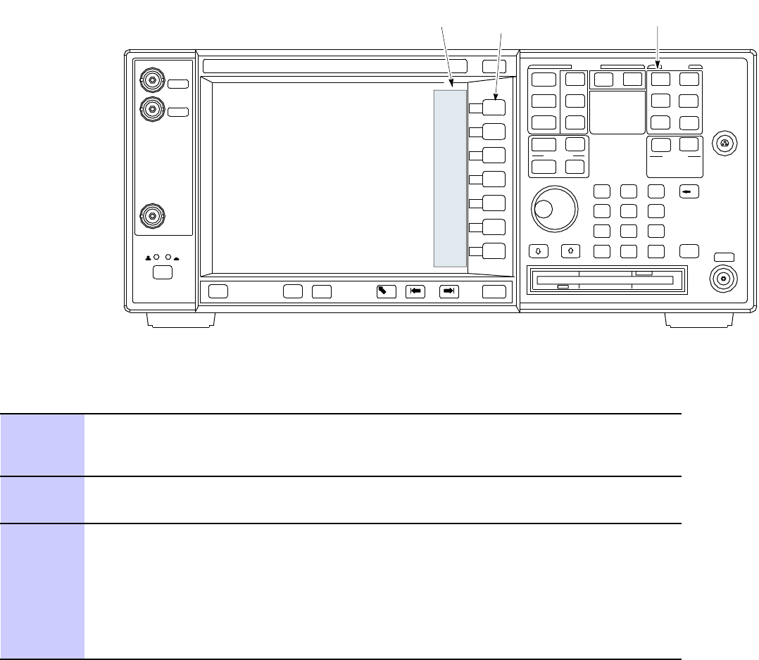
V erif ying and Setting GPIB Addresses – Agilent E4418 P ower Meter Appendix D: T est Equipment Prepar ation
Verifying and Setting GPIB Addresses – Agilent E4418
Power Meter■■■■■■■■■■■■■■■■■■■■■■■■■■■■■■■■■■■■■■■■■■■■■■■■■■■■■■■■■■■■■■
■
■
Figure D -9 Agilent E4418B P ower Meter V erif y and Set/Change GPIB Address
ti-cdma-05962.eps
LEFT DOWN UP RIGHT
ARROW
KEYS
PRESET/
LOCAL
SYSTEM/
INPUTS
STATUS
REPORTING
LINE
SOFTKEY
LABEL
AREA
SOFTKEY
MENU
TITLE
SOFTKEY
MENU PAGE
NUMBER
Refer to Figure D -9 when performing the following:
Procedure D -8 V erif y and Set/Change Agilent E4418 P ower Meter GPIB Address
1
If RMT (remote operation) is displayed on the left end of the instrument screen status
reporting line, press the Preset/Local front panel button.
Result: The status line entry will change to LCL (local or front panel operation).
2
On the instrument front panel, press the System/Inputs key .
Result: The softkey labels displayed on the right side of the instrument screen will
change.
3
Press the Remote Interface >Congure Interface >GPIB softkeys to the right of the
instrument screen.
Result:
•The softkey labels will change.
•The current instrument GPIB address will be displayed below the GP -IB Addr
softkey label.
D -18 68P09283A63 -5
FOA A UG 2007

1X UBS Macro B T S Optimization/A TP V erif ying and Setting GPIB Addresses – Agilent E4418 P ower Meter
Procedure D -8 V erif y and Set/Change Agilent E4418 P ower Meter GPIB Address
(Continued)
4
If the current GPIB address is set to 13 , skip to step step 8 .
5
If the current GPIB address is
not
set to 13 , press the GP-IB Addr softkey .
Result: A pop-up window will appear and display the current GPIB address.
6
Modify the GPIB address in the pop-up as necessary using the following front panel
keys to perform the indicated functions:
•Up and down arrow keys to change the digit on which the cursor is currently located
•Left and right arrow keys to move the cursor to other digits
7
When the GPIB address is correct, press the Enter softkey .
8
Return the instrument to the required setup configuration for testing.
68P09283A63 -5 D -19
A UG 2007 FOA
V erif ying and Setting GPIB Addresses – RS232 GPIB Interface Bo x Appendix D: T est Equipment Prepar ation
Verifying and Setting GPIB Addresses – RS232 GPIB
Interface Box■■■■■■■■■■■■■■■■■■■■■■■■■■■■■■■■■■■■■■■■■■■■■■■■■■■■■■■■■■■■■■
■
■
Be sure that the RS232 GPIB interface box DIP switches are set as shown in Figure D -10 .
Figure D -10 RS232 GPIB Interface Bo x
ti-cdma-00125.eps
RS232-GPIB
Interface Box
S MODE
DATA FORMAT
BAUD RATE
GPIB ADRS
ON
DIP SWITCH SETTINGS
G MODE
D -20 68P09283A63 -5
FOA A UG 2007
1X UBS Macro B T S Optimization/A TP T est Equipment Calibr ation – Agilent 4406 Self -alignment
Test Equipment Calibration – Agilent 4406
Self -alignment
■■■■■■■■■■■■■■■■■■■■■■■■■■■■■■■■■■■■■■■■■■■■■■■■■■■■■■■■■■■■■■
■
■
Refer to Figure D -11 when performing the following.
Figure D -11 Agilent E4406A Self -alignment
System
Key
Softkey
Buttons
Softkey Label
Display Area
ti-cdma-00126.eps
Procedure D -9 Agilent E4406A Self -alignment (Calibr ation)
1
In the SYSTEM section of the instrument front panel, press the System key .
Result: The softkey labels displayed on the right side of the instrument screen will
change.
2
Press the Alignments softkey button to the right of the instrument screen.
Result: The softkey labels will change.
3
Press the Align All Now softkey button.
Result:
•All other instrument functions will be suspended during the alignment.
•The display will change to show progress and results of the alignments performed.
•The alignment will take less than one minute.
68P09283A63 -5 D -21
A UG 2007 FOA
T est Equipment Calibr ation – Gigatronics 8542 P ower Meter Appendix D: T est Equipment Prepar ation
Test Equipment Calibration – Gigatronics 8542 Power
Meter
■■■■■■■■■■■■■■■■■■■■■■■■■■■■■■■■■■■■■■■■■■■■■■■■■■■■■■■■■■■■■■
■
■
Precise transmit output power calibration measurements are made using a bolometer -type
broadband power meter with a sensitive power sensor . F ollow the steps in Procedure D -10 to
enter information unique to the power sensor . Refer to Figure D -12 as necessary .
Figure D -12 Gigatronics 8541C P ower Meter Calibr ation
ti-cdma-00128.eps
CONNECT POWER SENSOR
WITH POWER METER
TURNED OFF
CONNECT POWER SENSOR TO
CALIBRATOR POWER REFERENCE
WHEN CALIBRATING/ZEROING UNIT
CALIBRATOR
ZERO
CAL FREQREL
MENU
ESCAPE
dB/MWRECALL
LOCAL
ENTER
A
MODE
GPIBPOWER
I
O
Giga-tronics8542CUniversalPowerMeter
dB m
- 1 0 0
LINEVOLTAGE
SELECTION GPIB
120VAC
FRONT View REAR View
GPIB CONNECTIONAC POWER
A
B
Procedure D -10 Calibr ate Gigatronics 8542 P ower Meter
1
Do not connect/disconnect the power meter sensor cable with AC power applied
to the meter . Disconnection could result in destruction of the sensing element
or miscalibr ation.
Make sure the power meter POWER pushbutton is OFF .
2
Connect the power sensor cable to the SENSOR input.
3
Set the POWER pushbutton to ON .
Allow the power meter and sensor to warm up and stabilize for a minimum of
60 minutes before performing the calibration procedure.
D -22 68P09283A63 -5
FOA A UG 2007

1X UBS Macro B T S Optimization/A TP T est Equipment Calibr ation – Gigatronics 8542 P ower Meter
Procedure D -10 Calibr ate Gigatronics 8542 P ower Meter (Continued)
4
Connect the power sensor to the CALIBRA TOR output connector .
5
Press ZERO , and wait for the process to complete.
Result: Sensor factory calibration data is read to power meter during this process.
6
When the zeroing process is complete, disconnect the power sensor from the
CALIBRA TOR output.
68P09283A63 -5 D -23
A UG 2007 FOA
D -24 68P09283A63 -5
FOA A UG 2007

A p p e n d i x
E
Optimization and Calibration Procedures
68P09283A63 -5 E -1
A UG 2007 FOA

Introduction to Calibr ation Appendix E: Optimization and Calibr ation Procedures
Introduction to Calibration■■■■■■■■■■■■■■■■■■■■■■■■■■■■■■■■■■■■■■■■■■■■■■■■■■■■■■■■■■■■■■
■
■
Overview
This appendix is not normally applicable to the UBS , but is provided for reference.
This section describes procedures for isolating the UBS from the span lines, preparing and
using the LMF , downloading system operating software, set up and calibration of the supported
test equipment, and transmit/receive path verification.
Before using the LMF , use a browser to view the
CA VEA TS
section in the
readme.html
file in the LMF home directory (e.g., c:\wlmf) for any applicable information.
Optimization Process Summary
A fter a UBS is physically installed and the preliminary operations, such as power up, have
been completed, the LMF is used to optimize the UBS . The basic optimization process consists
of the following:
E -2 68P09283A63 -5
FOA A UG 2007

1X UBS Macro B T S Optimization/A TP Introduction to Calibr ation
1. Use the status function and verify that all of the installed devices of the following types
respond with status information: HDModem and DMI.
2. V erify the code load of all the devices.
3. V erify the operation of the GPS and QHSO or MSO signals.
4. Unlock the following devices:
UBS
5. Connect the required test equipment for a full optimization.
6. Select the test equipment.
7. P erform the TX Audit.
8. If the TX Audit fails, there is a hardware problem, correct the problem that caused the
failure and repeat the optimization for the failed path.
9. If the TX Audit portion of the optimization passes for the RF path, but some of the TX or
RX tests fail, correct the problem that caused the failure and run the individual tests as
required until all TX and RX tests have passed for all the paths.
68P09283A63 -5 E -3
A UG 2007 FOA
T ak e Control of UBS R esources Appendix E: Optimization and Calibr ation Procedures
Take Control of UBS Resources■■■■■■■■■■■■■■■■■■■■■■■■■■■■■■■■■■■■■■■■■■■■■■■■■■■■■■■■■■■■■■
■
■
UBS Control
In a UBS , the DMI controls all UBS resources, such as the Modem and QHSO , which were
previously managed by the Central Base Station Controller (CBSC) and Mobility Manager
(MM) in BTSes. As a result, the LMF cannot perform any of the normal code/data download,
optimization, or test functions with the UBS until the DMI gives up control of these items.
Taking Control of UBS Resources
A fter logging into a UBS for optimization or acceptance testing, the first action which must be
performed is transferring control of the UBS from the Controller to the LMF
Prerequisites
LMF must be logged into the UBS .
after logging into the UBS , the LMF will be operating in monitoring mode. (It allows the user to
view status/monitor all UBS cards and Site Controller (SC))
T o take control of all devices from the UBS , perform UBS -> Enter
Invasive Mode
(DMI comes
under the control of the LMF and disconnects it from the UBS span lines).
E -4 68P09283A63 -5
FOA A UG 2007
1X UBS Macro B T S Optimization/A TP Code S yncing to the UBS
Code Syncing to the UBS■■■■■■■■■■■■■■■■■■■■■■■■■■■■■■■■■■■■■■■■■■■■■■■■■■■■■■■■■■■■■■
■
■
General Information
Before a UBS can operate, each equipped device must contain device application (RAM) code
and must be code sync’d to each equipped device by the user before the UBS can be made fully
functional for the site where it is installed
68P09283A63 -5 E -5
A UG 2007 FOA

Ba y Lev el Offset Calibr ation Appendix E: Optimization and Calibr ation Procedures
Bay Level Offset Calibration■■■■■■■■■■■■■■■■■■■■■■■■■■■■■■■■■■■■■■■■■■■■■■■■■■■■■■■■■■■■■■
■
■
T o avoid over -driving the XMIs, the BLO for UBS must be -2 dB or greater .
Introduction
Bay Level Offset (BLO) calibration is used to optimize non -standard UBS installations. F actory
calibration of the UBS components assures proper TX performance of the UBS system in all
installations that use Motorola supplied hardware in the TX path. In the event of a non -standard
installation, BLO calibration can be used to compensate for TX path loss variations due to
non -standard equipment.
RF Path Bay Level Offset Calibration
Calibration identifies the accumulated gain in every transmit path (sector–carrier) at the UBS
site and stores that value in a BLO data base calibration table in the LMF .
F or single frames, each receive path starts at an RX antenna port and terminates at the UBS .
Calibration identifies the accumulated gain in every transmit path at the UBS site and stores
that value in a BLO database. Only those slots (sectors) actually equipped in the current NEC
file are tested.
When to TX Audit
TX Audit will be performed:
•A fter initial UBS installation
•A fter UBS replacement
TX Path Calibration
The TX P ath Calibration assures correct site installation, cabling, and the first order functionality
of all installed equipment. The proper function of each RF path is verified during calibration.
The external test equipment is used to validate/calibrate the TX paths of the UBS .
E -6 68P09283A63 -5
FOA A UG 2007
1X UBS Macro B T S Optimization/A TP Ba y Lev el Offset Calibr ation
Before connecting an y test equipment directly to an y TX OUT connector y ou must
rst v erif y that there are no CDMA channels k ey ed. Ha v e the OMC –R place all
sectors under test OOS . F ailure to do so can result in serious personal injury and/or
equipment damage.
Alw a ys wear an appro v ed anti–static wrist str ap while handling an y circuit
card/module. If this is not done, there is a high probabilit y that the card/module
could be damaged b y ESD .
BLO Calibration Data File
During the calibration process, the LMF creates a UBS–#.cal calibration (BLO) offset data
file (CAL file) in the UBS–# folder . A fter calibration has been completed, Cal file has to be
downloaded to the UBS using UBS–>Upload CAL File function. An explanation of the file
is shown below .
Test Equipment Set -up for RF Path Calibration
F ollow the procedure in Procedure E -1 to set up test equipment.
Procedure E -1 T est Equipment Setup (RF P ath Calibr ation)
1
V erify the GPIB controller is properly connected and turned on (does not
apply to the Agilent E7495A/B).
T o prev ent damage to the test equipment, all tr ansmit (TX) test
connections must be via the 30 dB directional coupler . T otal cable
loss should be no less than 30 dB .
2
If it has not already been done, connect the LMF computer to the UBS LMT
connector on the UBS .
68P09283A63 -5 E -7
A UG 2007 FOA
Ba y Lev el Offset Calibr ation Appendix E: Optimization and Calibr ation Procedures
Transmit (TX) Path Calibration Description
The Line Maintenance F acility (LMF) will automatically use the channel numbers and power
levels assigned to the UBS if the UBS has been connected to an Operation Maintenance
Center — R adio (OMC -R) and brought into service. If the OMC -R connection has not yet been
established, the LMF operator will have to manually select each calibration point using a
specific channel number and power level for that channel. Bay Level Offset (BLO) calibration
is only applied to the specific channel numbers, thus calibration must be done on the exact
channel number to be used when the site is operational.
TX Calibration and the LMF
The LMF T ests > TX > TX Calibration... and T ests > All Cal/Audit... selections perform TX
BLO calibration testing for the installed RDF . The All Cal/Audit... selection initiates a series of
actions to perform TX calibration, and, if calibration is successful, download BLO and perform TX
audit. The TX Calibration... selection performs only TX calibration. When TX Calibration...
is used, BLO download and TX Audit must be performed as separate activities. The CDMA
T est P arameters window which opens when TX Calibration... or All Cal/Audit... is selected
contains several user–selectable features which are described in the following subsections.
Pilot Generation
Channels / Carrier pick–list containing the list of carriers available for the selected
Sector/Carriers. The list is derived from NECB file. DMI pick–list containing the list of DMIs
being able to generate Pilot signal of selected Sector/Carrier . The list is derived from NECB
file. The list is derived from NECB file. PN non–modifiable text box(es). The value is the
PilotPn derived from NECB files Carrier # Channels: text box(es). Carrier numbers and default
channels are derived from NECB file. Frequency Band non–modifiable text box(es). The value is
the frequency band derived from NECB files.
Verify BLO
In both the TX Calibration and All Cal/Audit dialog boxes, a V erify BLO checkbox is provided
and checked by default. A fter the actual TX calibration is completed during either the TX
Calibration or AllCal/Audit process, the BLO derived from the calibration is compared to a
standard, acceptable BLO tolerance for the UBS . In some installations, additional items may be
installed in the transmit path. The additional change in gain from these items could cause BLO
verification failure and, therefore, failure of the entire calibration. In these cases, either the
V erify BLO checkbox should be unchecked or the additional path losses should be added into
each applicable sector using the Util > Edit > TX Coupler Loss... function.
E -8 68P09283A63 -5
FOA A UG 2007

1X UBS Macro B T S Optimization/A TP Ba y Lev el Offset Calibr ation
Single–sided BLO Checkbox
Another option that appears in the pull–down menu is Single–sided BLO . Normally valid
BLO values are some value plus–or–minus some offset. Single–sided BLO spec is >–3.5 dB.
Double–sided BLO spec is –1.5 +/– 2.0 dB. T o get the more stringent conditions, the operator
checks Single–sided BLO when calibrating non -redundant transceivers. Single–sided BLO
carries the likelihood of more failures. This option should only be used by experienced CFEs.
The T ests > TX > TX Calibration... menu window has a T est P attern pull–down menu. This
menu has the following choices.
•Pilot (default) – performs tests using a pilot signal only . This pattern should be used when
running in–service tests. It requires the DMIs to do the test.
•Standard – performs the tests using pilot, synch, paging and six traffic channels.
•CDFPilot – performs the tests using the pilot signal, however , the gain is specified in the
NEC file. Advanced users may use CDFPilot to generate a Pilot pattern using the value
specified by the Pilot Gain parameter in the NEC file instead of a predetermined value.
•CDF – performs the tests using pilot, synch, paging and six traffic channels, however , the
gain for the channel elements is specified in the NEC file. Advanced users may use NEC to
generate a standard pattern. Instead of using the values specified by IS–97, the settings
for the following NEC parameters are used:
PilotGain
PchGain
SchGain
NomGain1W ay
68P09283A63 -5 E -9
A UG 2007 FOA

UBS R edundancy/Alarm T esting Appendix E: Optimization and Calibr ation Procedures
UBS Redundancy/Alarm Testing■■■■■■■■■■■■■■■■■■■■■■■■■■■■■■■■■■■■■■■■■■■■■■■■■■■■■■■■■■■■■■
■
■
Test Equipment Setup
F ollow the procedure in Procedure E -2 to set up test equipment:
All alarm tests are performed using the sector 1 IDRF .
Procedure E -2 T est Equipment Setup for R edundancy/Alarm T ests
1
Connect the LMF computer to the CRMS/LMT CUSTOMER ENET connector on the S SI.
2
Login to the UBS .
3
Set up test equipment for TX Audit at the sector 1 IDRF TX/RX M connector (see Figure 3-23 ,
Figure 3-24 ,Figure 3-25 , or Figure 3-26 ).
4
Display the alarm monitor by selecting Util > Alarm Monitor .
5
Unequip all customer–defined alarms reported through the S SI Customer I/O connectors
(IN 1–12 OUT 1–4 and IN 13–24 OUT 5–8) then selecting Device > Set Alarm Relays >
Unequipped .
During alarm reporting, spurious alarms may report. Allow the UBS to stabilize for
10 seconds. If any alarms are actively being reported after the UBS has stabilized,
determine the cause before proceeding further .
GPS and QHSO Redundancy/Alarm Tests
F ollow the procedure in Procedure E -3 to verify the manual redundancy of the GPS and QHSO
boards. V erification of alarms reported is also covered.
E -10 68P09283A63 -5
FOA A UG 2007
1X UBS Macro B T S Optimization/A TP UBS R edundancy/Alarm T esting
DO NOT
perform Procedure E -3 , unless the site is configured with an QHSO or
MSO time base as a backup for the GPS .
Procedure E -3 GPS and QHSO/MSO R edundancy/Alarm T ests
1
Before enabling an y XMI, alw a ys v erif y that the TX output is terminated into a 200
W non-r adiating RF load! F ailure to do so could result in serious personal injury
and/or damage to the equipment.
If the XMI is not INS (green), enable it by selecting it and then selecting Device > Unlock .
2
Click OK to close the status report window .
3
K ey the XMI by selecting it and then selecting Device > X CVR > K ey .
4
Disconnect the cable from the S SI RGPS connector . This forces the QHSO board time base to
become the CDMA timing source.
5
Observe that a CDMA timing reference alarm and source change are reported in the Alarm
Monitor .
6
Allow the QHSO/MSO to become the active timing source, and verify the following:
•The XMI remains keyed and INS .
•No other modules went OOS due to the transfer to QHSO/MSO reference.
7
Reconnect the cable to the S SI RGPS connector .
8
Allow the GPS to become the active timing source, and verify the following:
•The XMI remains keyed and INS .
•No other modules went OOS due to the transfer to GPS reference.
9
De-key the UBS by selecting Device > X CVR > Dekey .
10
Disable the XMI by selecting it and then selecting Device > Lock .
Result: The XMI color changes to yellow (OOS).
68P09283A63 -5 E -11
A UG 2007 FOA
Alarms T esting Appendix E: Optimization and Calibr ation Procedures
Alarms Testing■■■■■■■■■■■■■■■■■■■■■■■■■■■■■■■■■■■■■■■■■■■■■■■■■■■■■■■■■■■■■■
■
■
Alarm Verication
ALARM connectors provide Customer Alarm Inputs and Outputs. The customer can connect
UBS site alarm input sensors and output devices to the UBS , thus providing alarm reporting of
active sensors as well controlling output devices.
Alarm Reporting Display
The Alarm Monitor window can be displayed to list alarms that occur after the window is
displayed. T o access the Alarm Monitor window , select Util>Alarm Monitor .
The following buttons are included:
•The Options button allows for a severity level (W arning, Minor , and Major) selection.
The default is all levels. T o change the level of alarms reported click on the Options
button and highlight the desired alarm level(s). T o select multiple levels press the Ctrl
key (for individual selections) or Shift key (for a range of selections) while clicking on
the desired levels.
•The Pause button pauses/stops the display of alarms. When the Pause button is clicked
the name of the button changes to Continue . When the Continue button is clicked, the
display of alarms continues. Alarms that occur between the time the Pause button is
clicked and the Continue button is clicked are not displayed.
•The Clear button clears the Alarm Monitor display . New alarms that occur after the Clear
button is clicked are displayed.
•The Dismiss button dismisses/closes the Alarm Monitor display .
E -12 68P09283A63 -5
FOA A UG 2007
1X UBS Macro B T S Optimization/A TP Alarms T esting
Figure E -1 Alarm Connector Location
ti-cdma-05698-A.eps
CUSTOMER
EQUIPMENT
68P09283A63 -5 E -13
A UG 2007 FOA

Alarms T esting Appendix E: Optimization and Calibr ation Procedures
Purpose
The following procedures verify the customer defined alarms and relay contacts are functioning
properly . These tests are performed on all alarms/relays in a sequential manner until all have
been verified. P erform these procedures periodically to ensure the external alarms are reported
properly . F ollowing these procedures ensures continued peak system performance.
Study the site engineering documents and perform the following tests only after first verifying
that the alarm cabling configuration required to interconnect the UBS frame with external
alarm sensors and/or relays meet requirements called out in the 1X UBS Macro BTS Hardware
Installation .
Motorola highly recommends that you read and understand this procedure in its
entirety before starting this procedure.
Alarm input and output information
Alarm connectors
There are two ALARM connectors on the UBS Macro S SI:
•CUSTOMER IP 1 -12 OP 1 -4 connector
•CUSTOMER IP 13 -24 OP 5 -8 connector
Each ALARM connector provides 12 inputs and 4 outputs. A total of 24 inputs and 8 outputs are
available.
Function
ALARM connectors provide for Customer Alarm Inputs and Outputs. The customer can connect
UBS site alarm input sensors and output devices to the UBS , thus providing alarm reporting of
active sensors as well as controlling output devices.
The S SI detects signals from customer input sensors and reports the detected signals to the
DMI controller , which in turn reports the detected alarm to the OMC -R, where it is displayed as
defined by the customer .
The S SI also provides switched relay contacts to customer output devices. The S SI controls
relay contacts according to output control signals from the DMI controller , in response to
customer defined commands entered at the OMC -R.
E -14 68P09283A63 -5
FOA A UG 2007
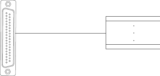
1X UBS Macro B T S Optimization/A TP Alarms T esting
Input connectors
Each input consists of a wire/pin pair (that is, input/Gnd). T o ensure proper operation, each
pair to be used must be connected to an external sensor that provides a dry -contact closure.
The customer sensor output connects between an optically isolated 5 VDC signal and an
isolated return.
F or an OPEN circuit (logic 0) between pins:
•There is 10 K Ohms or greater across the input pair .
•The signal to ground voltage is +5 VDC .
F or a CLOSED circuit (logic 1) between pins:
•There is 1 K Ohms or less across the input pair .
•The signal to ground current is a maximum of 9 mA.
Either of the above states can be defined by the customer in system software as an alarm
condition.
Output connectors
Each output consists of 3 -wires/pins:
•COM
•NC
•NO
The customer output device control inputs connect between the common (COM) and either the
normally closed (NC) or normally open (NO) contacts of a relay . The NC and NO state for relay
contacts occurs when the relay coil is not energized.
Relay contacts are load rated for a maximum of 1 A at 24 VDC and 0.5 A at 50 VDC .
The toggling of relay contacts to the opposite state is controlled by system software.
Figure E -2 Alarm Connector Pin Numbering
ti-cdma-05692.eps
LOOSE WIRES, NO CONNECTOR
37-Pin-Type
(Male)
1
19 37
20
68P09283A63 -5 E -15
A UG 2007 FOA

Alarms T esting Appendix E: Optimization and Calibr ation Procedures
Customer Alarm Input Verication
Procedure E -4 describes how to test the Customer alarm input verification. F ollow the steps as
instructed and compare results with the LMF display .
It may take a few seconds for alarms to be reported. The default delay is 5 seconds.
When shorting alarm pins wait for the alarm report before removing the short.
Procedure E -4 Customer Alarm Input V erication
1
Connect the LMF to the UBS and log into the UBS .
2
Select the Controller .
3
Click on the Device menu.
4
Click on the Set Alarm Relays menu item.
5
Click on Normally Open .
A status report window displays the results of the action.
6
Click on OK to close the status report window .
7
Refer to Figure E -2 and sequentially short the ALARM
A connector CA IN 1 through CA IN 12 pins together .
Sequentially short the ALARM B connector
CA IN 13 through CA IN 24 pins together .
An alarm should be reported for each pair of pins that are shorted.
A clear alarm should be reported for each pair of pins when the short
is removed.
8
Select the Controller .
9
Click on the Device menu.
10
Click on the Set Alarm Relays menu item.
1 1
Click on Normally Closed .
A status report window displays the results of the action.
12
Click on OK to close the status report window .
Alarms should be reported for alarm inputs 1 through
24.
13
Sequentially short the ALARM B connector
CA IN 13 through CA IN 24 pins together .
A clear alarm should be reported for each pair of pins that are shorted.
An alarm should be reported for each pair of pins when the short is removed.
14
Select the Controller .
15
Click on the Device menu.
E -16 68P09283A63 -5
FOA A UG 2007

1X UBS Macro B T S Optimization/A TP Alarms T esting
Procedure E -4 Customer Alarm Input V erication (Continued)
16
Click on the Set Alarm Relays menu item.
17
Click on Unequipped .
A status report window displays the results of the action.
18
Click on OK to close the status report window .
19
Refer to Figure E -2 and sequentially short the ALARM
A connector CA IN 1 through CA IN 12 pins together .
Sequentially short the ALARM B connector
CA IN 13 through CA IN 24 pins together .
No alarms should be displayed.
20
Load data to the Controller to reset the alarm relay conditions according
to the NEC file.
Pin and Signal Information for Alarm Connectors
T able E -1 and T able E -2 lists the pins, wire color codes, and signal names.
Table E -1 Connector Pinout for Cable T IP 1–12 OP 1–4
Pin Name
Recommended W ire Color for Cable
1 CA IN 1
White/Blue
2 CA IN 2
White/Orange
3 CA IN 3
White/Green
4 CA IN 4
White/Brown
5
CA IN 5
White/Gray
6 CA IN 6
Red/Blue
7
CA IN 7
Red/Orange
8 CA IN 8
Red/Green
9 CA IN 9
Red/Brown
10 NC
NA
11 CA NO 1
Black/Blue
12 CA NO 2
Black/Orange
13 CA NC 2
Black/Green
14 CA NO 3
Black/Brown
15 CA NO 4
Black/Gray
16 CA NC 4
Y ellow/Blue
17 CA IN 10
Y ellow/Orange
18 CA IN 11
Y ellow/Green
19 CA IN 12
Y ellow/Brown
68P09283A63 -5 E -17
A UG 2007 FOA

Alarms T esting Appendix E: Optimization and Calibr ation Procedures
Table E -1 Connector Pinout for Cable T IP 1–12 OP 1–4 (Continued)
Pin Name
Recommended W ire Color for Cable
20 GND 1
Blue/White
21 GND 2
Orange/White
22 GND 3
Green/White
23 GND 4
Brown/White
24 GND 5
Gray/White
25 GND 6
Blue/Red
26 GND 7
Orange/Red
27 GND 8
Green/Red
28 GND 9
Brown/Red
29 CA NC 1
Blue/Black
30 CA COM 1
Orange/Black
31 CA COM 2
Green/Black
32 CA NC 3
Brown/Black
33 CA COM 3
Gray/Black
34 CA COM 4
Blue/Y ellow
35 GND 10
Orange/Y ellow
36 GND 11
Green/Y ellow
37 GND 12
Brown/Y ellow
CA IN— Customer Alarm signal into the M810 BTS , NO — Normally Open, NC — Normally Closed,
COM — Common
Table E -2 Connector Pinout for Cable T IP13–24 OP5–8
Pin Name
Recommended W ire Color for Cable
1 CA IN 13
White/Blue
2 CA IN 14
White/Orange
3 CA IN 15
White/Green
4 CA IN 16
White/Brown
5
CA IN 17
White/Gray
6 CA IN 18
Red/Blue
7
CA IN 19
Red/Orange
8 CA IN 20
Red/Green
9 CA IN 21
Red/Brown
10 NC
NA
E -18 68P09283A63 -5
FOA A UG 2007

1X UBS Macro B T S Optimization/A TP Alarms T esting
Table E -2 Connector Pinout for Cable T IP13–24 OP5–8 (Continued)
Pin Name
Recommended W ire Color for Cable
11 CA NO 5
Black/Blue
12 CA NO 6
Black/Orange
13 CA NC 6
Black/Green
14 CA NO 7
Black/Brown
15 CA NO 8
Black/Gray
16 CA NC 8
Y ellow/Blue
17 CA IN 22
Y ellow/Orange
18 CA IN 23
Y ellow/Green
19 CA IN 24
Y ellow/Brown
20 GND 13
Blue/White
21 GND 14
Orange/White
22 GND 15
Green/White
23 GND 16
Brown/White
24 GND 17
Gray/White
25 GND 18
Blue/Red
26 GND 19
Orange/Red
27 GND 28
Green/Red
28 GND 21
Brown/Red
29 CA NC 5
Blue/Black
30 CA COM 5
Orange/Black
31 CA COM 6
Green/Black
32 CA NC 7
Brown/Black
33 CA COM 7
Gray/Black
34 CA COM 8
Blue/Y ellow
35 GND 22
Orange/Y ellow
36 GND 23
Green/Y ellow
37 GND 24
Brown/Y ellow
CA IN— Customer Alarm signal into the M810 BTS , NO — Normally Open, NC — Normally Closed,
COM — Common
68P09283A63 -5 E -19
A UG 2007 FOA
E -20 68P09283A63 -5
FOA A UG 2007

A p p e n d i x
F
MSO Calibration
68P09283A63 -5 F -1
A UG 2007 FOA

MSO Calibr ation Appendix F : MSO Calibr ation
MSO Calibration
■■■■■■■■■■■■■■■■■■■■■■■■■■■■■■■■■■■■■■■■■■■■■■■■■■■■■■■■■■■■■■
■
■
MSO Calibration Status
The check the status of the Motorola Standard (Medium Stability) Oscillator (MSO) perform the
following:
•Log into the UBS with the LMF .
•Click on BTS > MSO Calibration Status menu item
•MSO status is displayed.
MSO Calibration Procedure
P erform the following procedure only if the BTS is in
Island Mode
configuration, the system has
no configured references, and HSO , GPS , or external reference is connected.
Procedure F -1 Procedure to Calibr ate the MSO
1
Log into the UBS .
2
Click on BTS Menu . Select Enter Invasive Mode (Figure F -1 ). W ait for
Message window to appear ( Figure F -2 ).
3
From BTS Menu, select MSO Calibration Status (Figure F -3 ). MSO status is
displayed ( Figure F -4 )
4
From BTS Menu, select MSO Calibration Figure F -5 )
5
Select Clock reference HSO-1 to start MSO calibration ( Figure F -6 ).
W ait for start ( Figure F -7 )
6
The calibration takes about 15 minutes to
complete (it can take up to an 60 minutes).
Read the calibration status ( Figure F -8 )
7
Logout of UBS . Click on File->Exit (Figure F -9 ).
8
Login to UBS (do not enter invasive mode).
9
From BTS Menu, select MSO Calibration Status (Figure F -10 ).
F -2 68P09283A63 -5
FOA A UG 2007
1X UBS Macro B T S Optimization/A TP MSO Calibr ation
Figure F -1 B T S Menu - Enter In v asiv e Mode
Figure F -2 Message Window
Figure F -3 B T S Menu - MSO CAL Status
Figure F -4 R ead MSO Cal Status
Figure F -5 Select MSO Calibr ation
Figure F -6 Select Clock R eference
Figure F -7 MSO Calibr ation (In v asiv e Mode)
Figure F -8 R ead MSO Status
Figure F -9 Exit Local T erminal
Figure F -10 MSO Status (Non -In v asiv e Mode)
68P09283A63 -5 F -3
A UG 2007 FOA
F -4 68P09283A63 -5
FOA A UG 2007

A p p e n d i x
G
SSI Loopback Connector Information
68P09283A63 -5 G -1
A UG 2007 FOA
S SI Loopback Connector Appendix G: S SI Loopback Connector Information
SSI Loopback Connector■■■■■■■■■■■■■■■■■■■■■■■■■■■■■■■■■■■■■■■■■■■■■■■■■■■■■■■■■■■■■■
■
■
There are two loopback connectors required, one for the Span and one for the Customer Input /
Output. This appendix section provides the information necessary for making a 37 pin D -sub for
the span and customer input / output connectors.
Purpose
The purpose of the S SI loopback connector is to enable the user to determine if the receive and
transmit lines of the span cable circuitry are operating correctly .
Required Parts
Should a 37 pin D -sub loopback connector not be available, one can be made by the user to
interface with the 37 pin D -sub on the S SI board.
Table G -1 P arts R equired to F abricate Loopback Connector
Item Part Number
Qty
Description
Customer Supplied
2
37 pin, D -sub plug
Figure G -1 Loopback Connector
ti-cdma-05692-A.eps
37-Pin-Type
(Male)
119
37
20
SSI Span Loopback Connector
The pinouts for the S SI Span Loopback Connector are listed in T able G -2 . Recommended wire is
22 A WG , solid or 24 A WG , stranded.
G -2 68P09283A63 -5
FOA A UG 2007

1X UBS Macro B T S Optimization/A TP S SI Loopback Connector
Table G -2 S SI Span Loopback Connector Pinouts
Pin #
Signal
Description
Loopback
Connection Pin
Pin #
Signal
Description
Loopback
Connection Pin
1 TX1 TIP 12 20 TX1 RING 30
2 TX2 TIP 13 21 TX2 RING 31
3 TX3 TIP 14 22 TX3 RING 32
4 TX4 TIP 15 23 TX4 RING 33
5 TX5 TIP
16 24 TX5 RING 34
6 TX6 TIP 17 25 TX6 RING 35
7 TX7 TIP
18 26 TX7 RING 36
8 TX8 TIP 19 27 TX8 RING 37
9 GND 28 GND
10 GND 29 GND
11 GND 30 RX1 RING 20
12 RX1 TIP 1 31 RX2 RING 21
13 RX2 TIP 2 32 RX3 RING 22
14 RX3 TIP 3 33 RX4 RING 23
15 RX4 TIP 4 34 RX5 RING 24
16
RX5 TIP 5
35 RX6 RING 25
17 RX6 TIP 6 36 RX7 RING 26
18
RX7 TIP 7
37 RX8 RING 27
19 RX8 TIP 8
68P09283A63 -5 G -3
A UG 2007 FOA
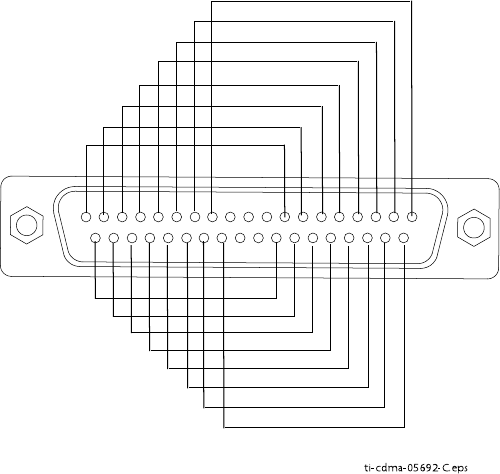
S SI Loopback Connector Appendix G: S SI Loopback Connector Information
Figure G -2 S SI Span Loopback Connector Wiring Diagr am
ti-cdma-05692-C.eps
20 37
19
1
30
12
SSI Customer Input / Output Loopback Connector
The pinouts for the S SI CIO Loopback Connector are listed in T able G -3 . Recommended wire is
22 A WG , solid or 24 A WG , stranded.
G -4 68P09283A63 -5
FOA A UG 2007

1X UBS Macro B T S Optimization/A TP S SI Loopback Connector
Table G -3 S SI CIO Loopback Connector Pinouts
Pin #
Signal
Description
Loopback
Connection Pin
Pin #
Signal
Description
Loopback
Connection Pin
1 CA IN 1 30 20 GND 13
2 CA IN 2 30 21 GND
3 CA IN 3 30 22 GND
4 CA IN 4 31 23 GND 16
5
CA IN 5 31 24 GND
6 CA IN 6 31 25 GND
7
CA IN 7 33 26 GND 32
8 CA IN 8 33 27 GND
9 CA IN 9 33 28 GND 29
10 NC 29
Relay NC 1
28
11
Relay NO 1
NC 30
Relay COM 1
1,2,3
12
Relay NO 2
NC 31
Relay COM 2
4,5,6
13
Relay NC 2
20 32
Relay NC 3
26
14
Relay NO 3
NC 33
Relay COM 3
7,8,9
15
Relay NO 4
NC 34
Relay COM 4
17,18,19
16
Relay NC 4
23 35 GND
17 CA IN 10 34 36 GND
18 CA IN 11 34 37 GND
19 CA IN 12 34
68P09283A63 -5 G -5
A UG 2007 FOA
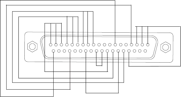
S SI Loopback Connector Appendix G: S SI Loopback Connector Information
Figure G -3 S SI CIO Loopback Connector Wiring Diagr am
ti-cdma-05692-B.eps
119
34
20
9
23
13
26
G -6 68P09283A63 -5
FOA A UG 2007

Index
Index
■■■■■■■■■■■■■■■■■■■■■■■■■■■■■■■■■■■■■■■■■■■■■■■■■■■■■■■■■■■■■■
■
■
■
■
A
Abbreviations and Acronyms
Computer Requirements, Minimum . . . 1 - 13
Acceptance T esting . . . . . . . . . . . . . 1 - 5
Advantest R3267
GPIB Address . . . . . . . . . . . . . . D - 11
Advantest R3465
Calibrating T est Cable . . . . . . . . . . D - 2
Advantest R3562
GPIB Address . . . . . . . . . . . . . . D - 13
Agilent 8935 Series E6380 (formerly HP 8935)
T est Set GPIB Address . . . . . . . . . . D - 14
Agilent E4406A
calibration . . . . . . . . . D - 3 , D - 21 to D - 22
GPIB Address . . . . . . . . . . . . . . . D - 7
Agilent E4432B Signal Generator
GPIB Address . . . . . . . . . . . . . . . D - 9
A TP T est Matrix
FRU Optimization . . . . . . . . . . . . . B - 2
B
Backhaul Configuration Procedure . . . . . 5 - 2
Bay Level Offset Calibration
Bay Level Offset Calibration (contd.)
Calibration, BLO . . . . . . . . . . . . . E - 6
C
Cable
Calibrating . . . . . . . . . . . . . . . 3 - 64
Setting Loss V alues . . . . . . . . . . . 3 - 72
Cable Calibration
Manual ................. 3-35
Cable Calibration Set -up
Automatic . . . . . . . . . . . . . . . . 3 - 35
Calibrate T est Cabling
Communications System Analyzer . . . 3 - 64
Calibrating
Cables . . . . . . . . . . . . . . . . . 3 - 64
T est Equipment . . . . . . . . . . . . . 3 - 56
Calibrating T est Cable
Advantest R3465 . . . . . . . . . . . . . D - 2
Calibrating T est Cabling
Calibrating T est Cabling using Communications
System Analyzer . . . . . . . . . . . . 3 - 69
calibration
Gigatronics 8542B . . . . . . . . . . . D - 22
Calibration . . . . . . . . . . . . . . . . . 1 - 4
Calibration Procedures Included
Automatic . . . . . . . . . . . . . . . . 3 - 56
Calibration, T est Cable . . . . . . . . . . . 1 - 7
Calibration, T est Equipment . . . . . . . . 1 - 7
Code Domain A TP
Noise Floor A TP . . . . . . . . . . . . . 4 - 21
Continuous W aveform, Lock . . . . . . . . 4 - 25
Continuous W aveform, Unlock . . . . . . 4 - 24
D
Documents, Required . . . . . . . . . . . 1 - 13
E
E4406A
68P09283A63 -5 IX -1
A UG 2007 FOA

Index
E4406A (contd.)
calibration . . . . . . . . . D - 3 , D - 21 to D - 22
F
FER ATP ................. 4-23
G
Generate A TP Report . . . . . . . . . . . 4 - 26
Gigatronics 8541C power meter . . . . . . D - 3
Gigatronics 8542 power meter
calibration . . . . . . . . . . . . . . . D - 22
Gigatronics 8542B power meter
illustration . . . . . . . . . . . . . . . D - 16
GPIB
power meter
Gigatronics 8542B . . . . . . . . . . D - 16
GPIB Address
Advantest R3267 . . . . . . . . . . . . D - 11
Advantest R3562 . . . . . . . . . . . . D - 13
Agilent (formerly HP) 8935 . . . . . . . D - 14
Agilent E4406A . . . . . . . . . . . . . . D - 7
Agilent E4432B . . . . . . . . . . . . . . D - 9
I
IP Addresses
Agilent E7495A . . . . . . . . . . . . . 3 - 47
L
LMF Hardware Requirements
Computer Requirements, Minimum . . . . 1 - 9
LMF Operation . . . . . . . . . . . . . . . 3 - 1
M
MSO Calibration
Calibration MSO . . . . . . . . . . . . . F - 2
MSO Calibration Procedure
Calibration Procedure, MSO . . . . . . . F - 2
O
Optimization and Calibration Procedures . . E - 1
Optimization, P eriodic . . . . . . . . . . . 1 - 6
Optimization/A TP Checklist
CHecklist, Optimization/A TP . . . . . . . A - 2
Optimization/A TP Setup . . . . . . . . . . 3 - 40
Optional Full A TP T est Matrix
Full A TP T est Matrix . . . . . . . . . . . B - 2
P
Pilot Time Offset A TP
IX -2 68P09283A63 -5
FOA A UG 2007

Index
Pilot Time Offset A TP (contd.)
PTO A TP . . . . . . . . . . . . . . . . 4 - 19
P ower meter
GPIB
Gigatronics 8542B . . . . . . . . . . D - 16
P ower meter (contd.)
illustration
Gigatronics 8542B . . . . . . . . . . D - 16
R
Reduced A TP . . . . . . . . . . . . . . . . B - 2
Reference Documents . . . . . . . . . . . 1 - 13
Rho A TP
Rho A TP (contd.)
TX W aveform Quality A TP . . . . . . . . 4 - 18
RS232 GPIB Interface Box . . . . . . . . D - 20
S
Selecting T est Equipment . . . . . . . . . 3 - 47
Setting Cable Loss V alues . . . . . . . . . 3 - 72
Setup for Optimization/A TP . . . . . . . . 3 - 40
Signal Generator . . . . . . . . . . . 3 - 71 , 3 - 4
Spectrum Analyzer . . . . . . . . . . 3 - 71 , 3 - 4
Spectrum Analyzer . . . . . . . . . . . 3 - 33
T
T est Equipment
Automatically Selecting . . . . 3 - 50 , 3 - 52 , 3 - 54
Calibrating . . . . . . . . . . . . . . . 3 - 56
Connecting test equipment to the BTS . . 3 - 32
Selecting . . . . . . . . . . . . . . . . 3 - 48
T est Equipment GPIB Address Settings
GPIB Address Settings, T est Equip
ment .................. 3-32
T est Equipment Preparation . . . . . . . . D - 2
T est Equipment Setup, Agilent E7495
Agilent E7495 Setup . . . . . . . . . . . D - 4
T est Equipment, Supported . . . . . . . . 3 - 33
T est Set Calibration
Background . . . . . . . . . . . . . . . 3 - 55
TX and RX A TP . . . . . . . . . . . . . . . 4 - 4
TX Mask A TP
TX Spectral Purity Transmit Mask A TP . . 4 - 17
U
UBS Component Identification . . . . . . 1 - 21
W
W arm -up Equipment . . . . . . . . . . . 3 - 34
68P09283A63 -5 IX -3
A UG 2007 FOA