Nokia Solutions and Networks T5JX1 UBS CDMA XMI Transceiver at 800 MHz User Manual Exhibit 8f
Nokia Solutions and Networks UBS CDMA XMI Transceiver at 800 MHz Exhibit 8f
UserManual.wiki
>
Nokia Solutions and Networks
>
T5JX1 User Manual
>
Exhibit 8f
Contents
1.
Exhibit 8a
2.
Exhibit 8b
3.
Exhibit 8c
4.
Exhibit 8d
5.
Exhibit 8e
6.
Exhibit 8f
Exhibit 8f
Navigation menu
Upload a User Manual
Namespaces
Wiki Guide
HTML
PDF
Info
Views
User Manual
Discussion / Help
Navigation
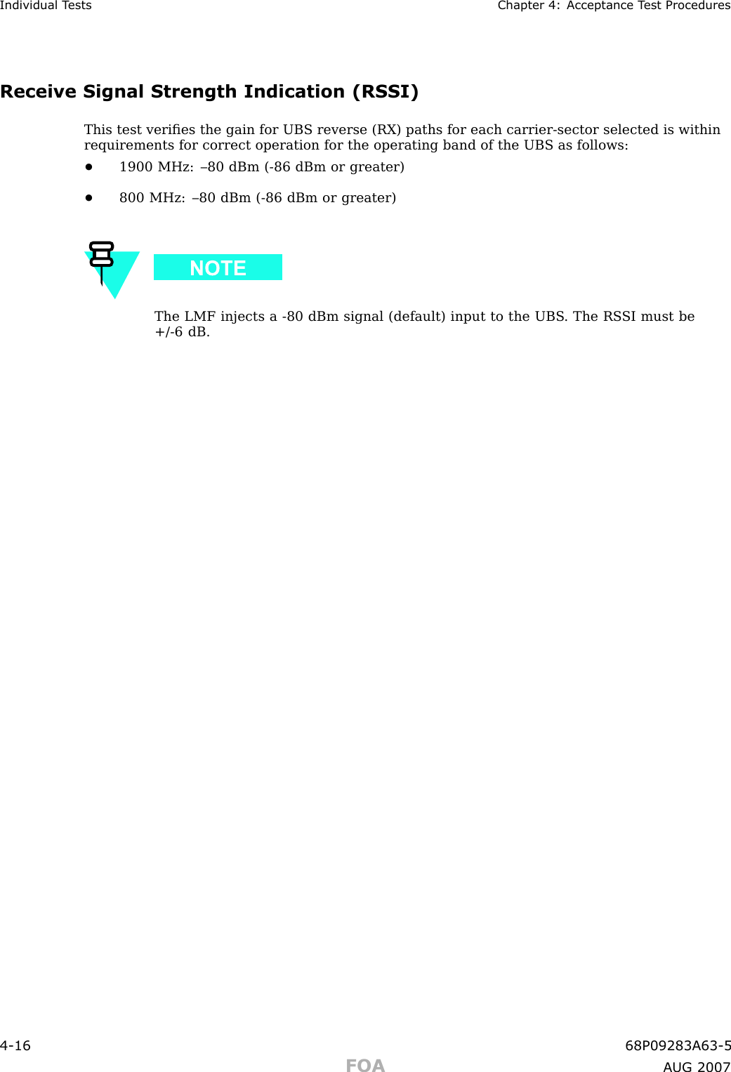
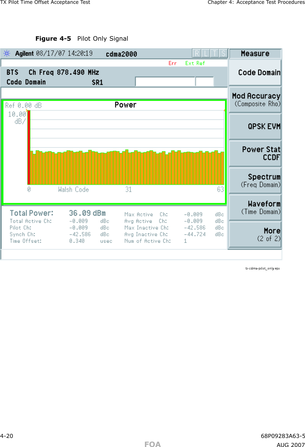
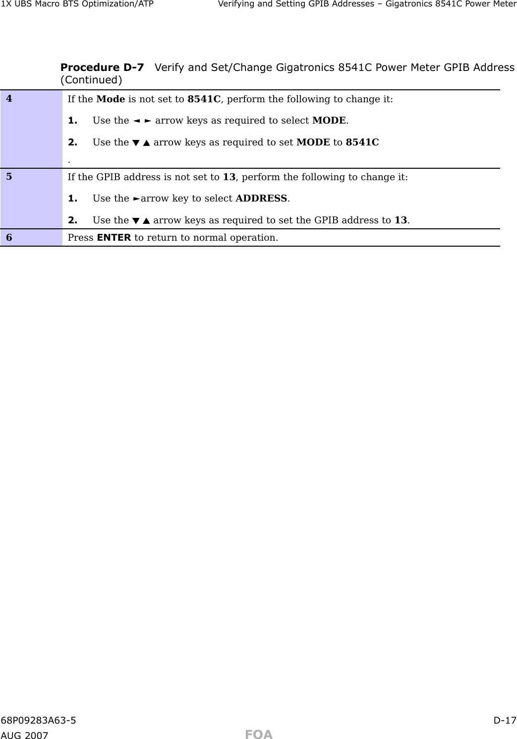
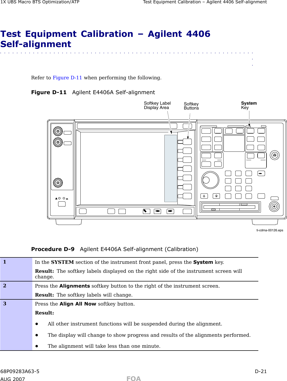
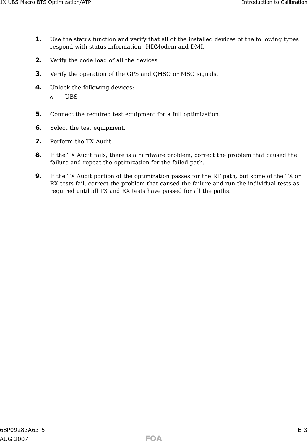
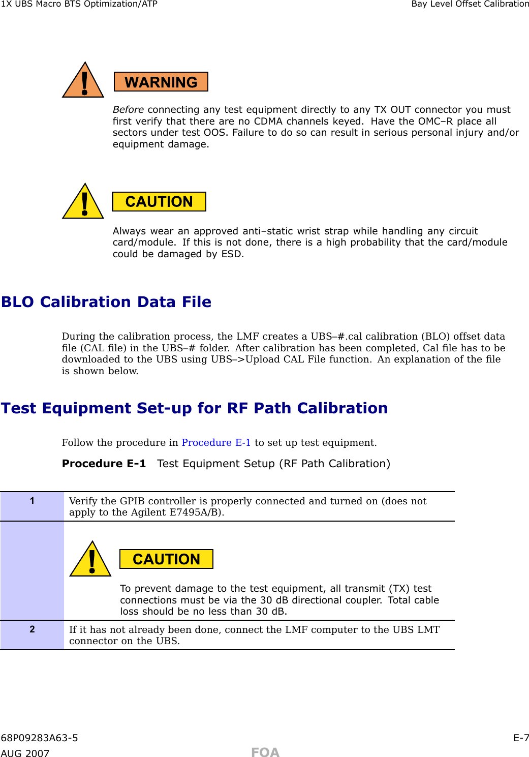
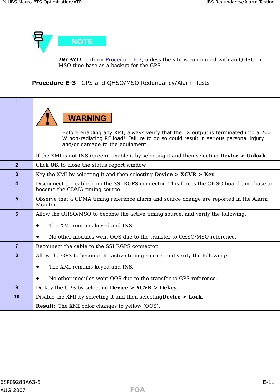
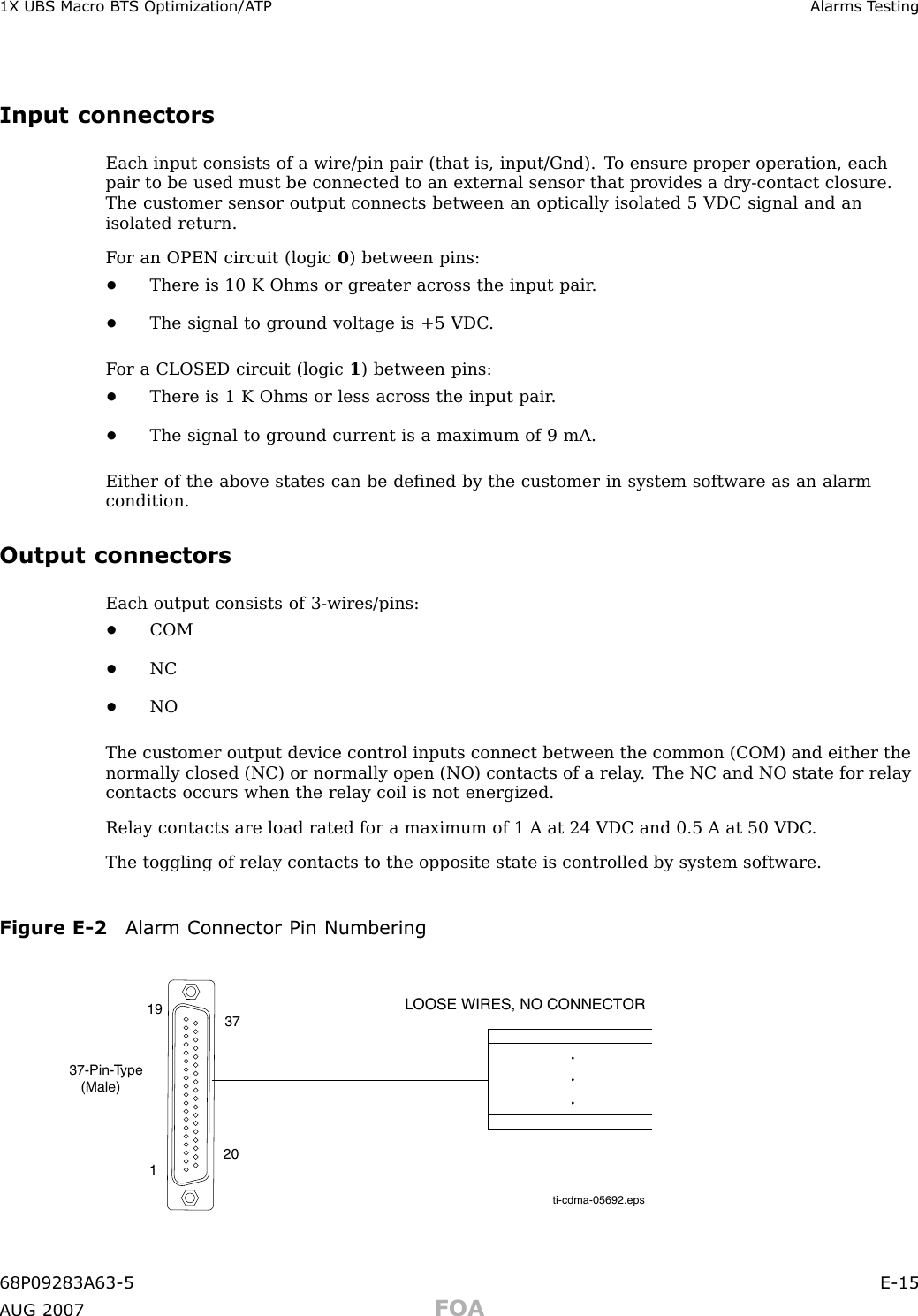
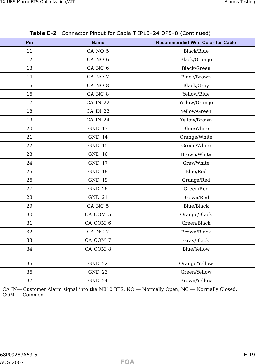
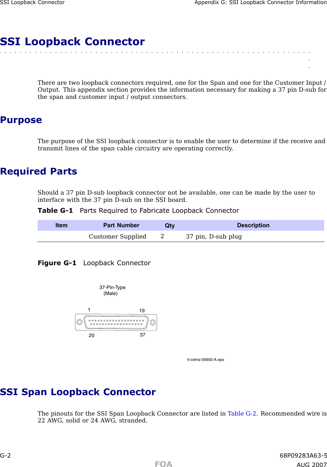
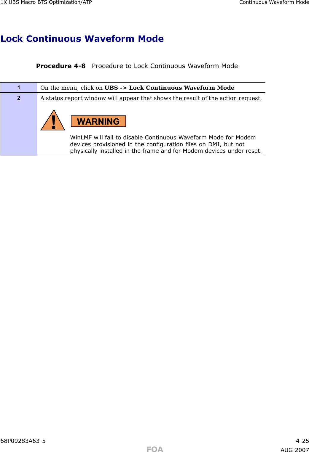
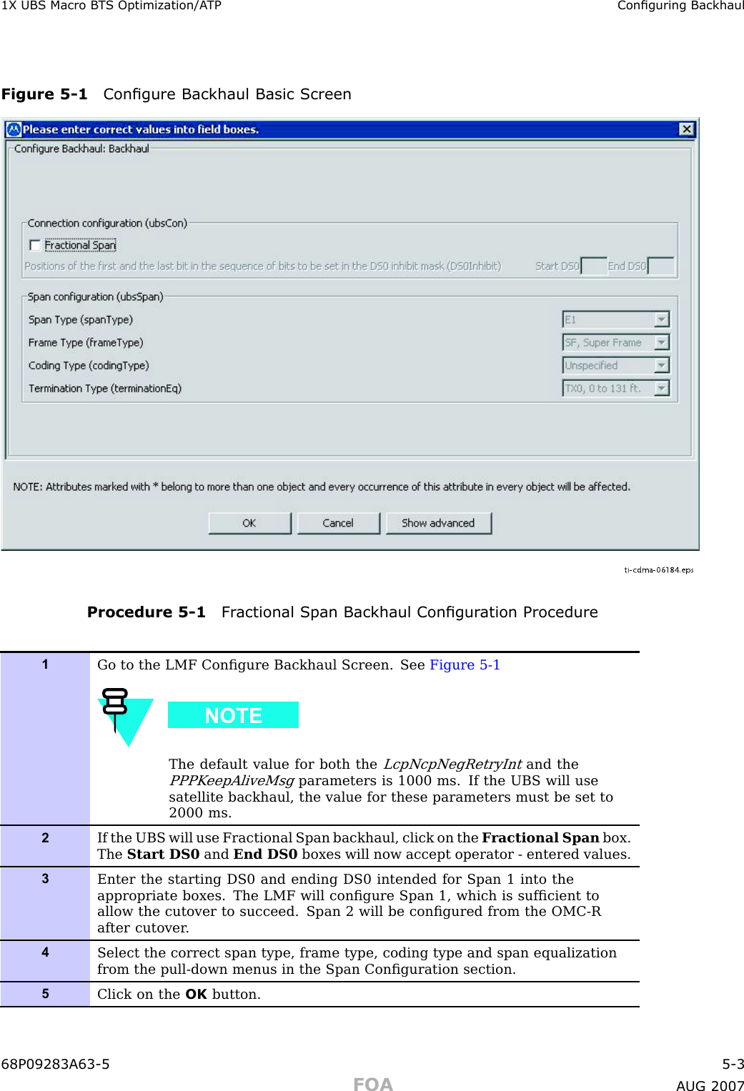
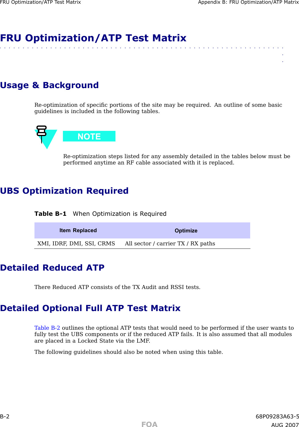
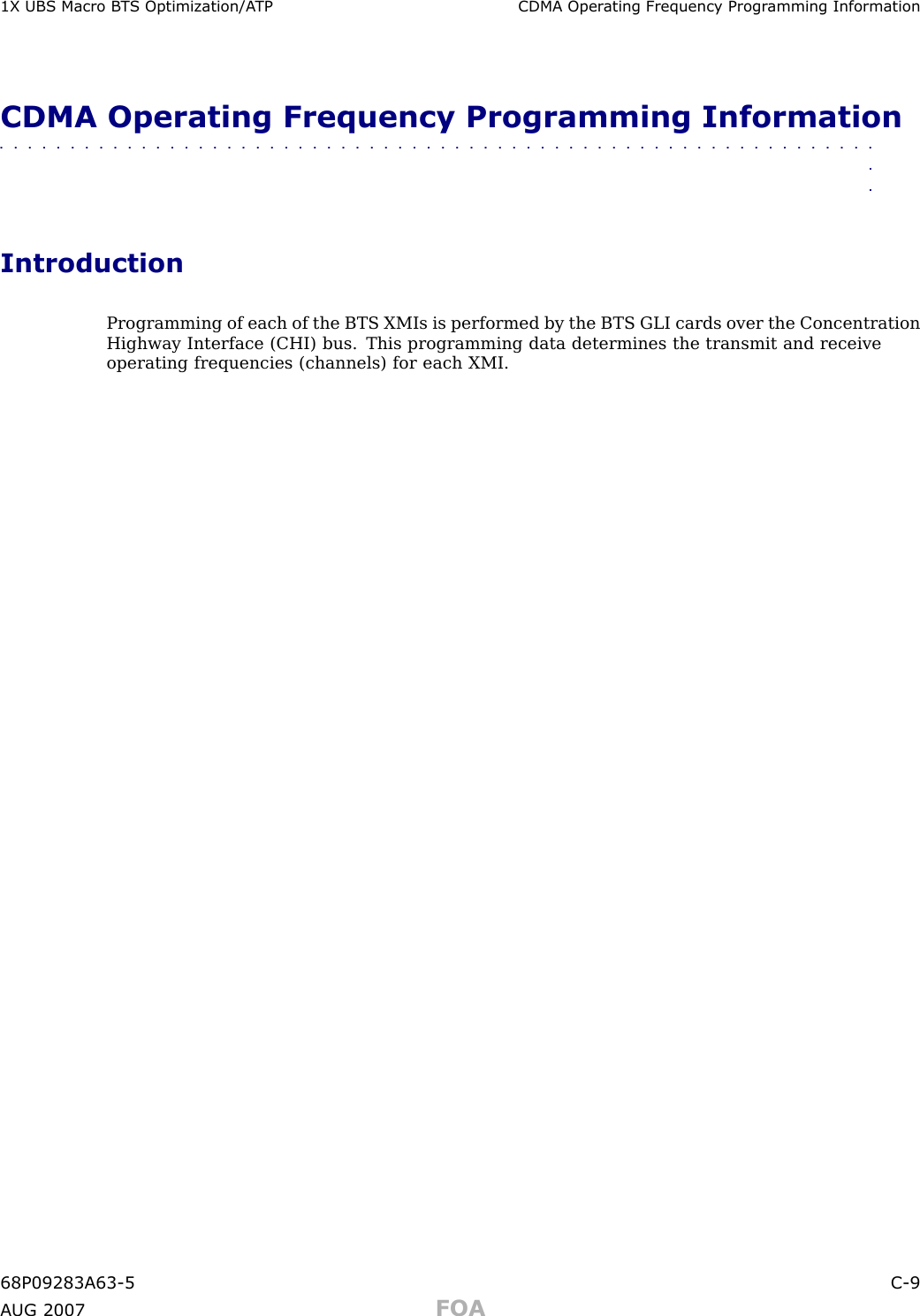
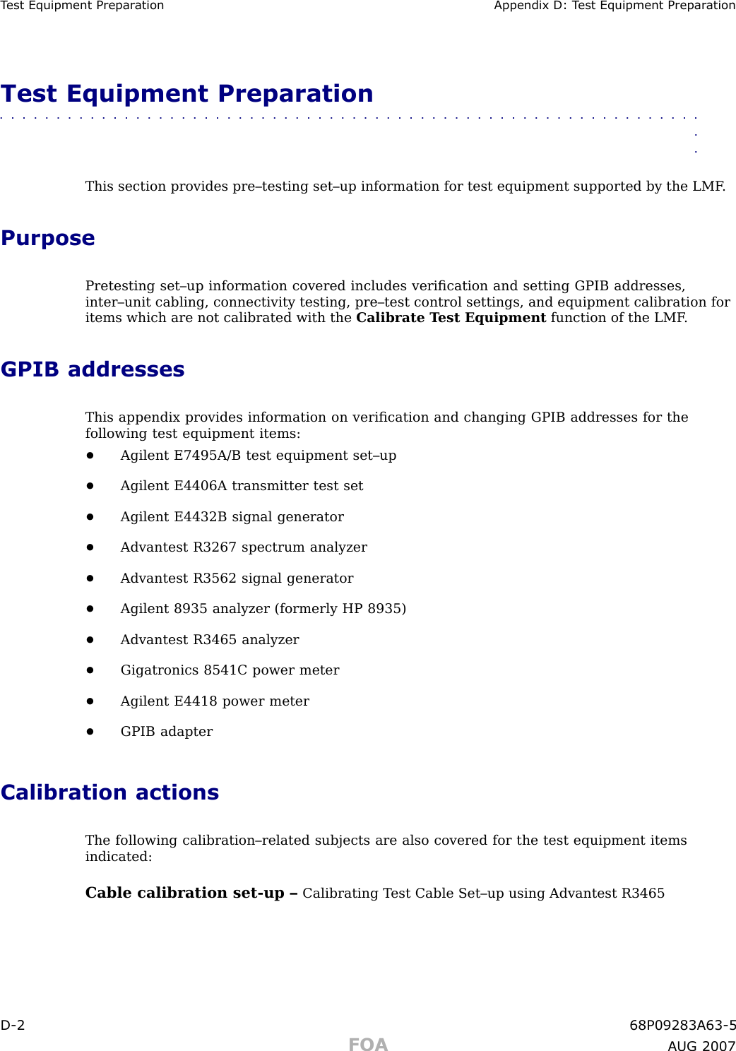
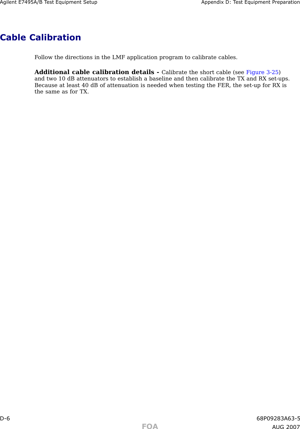
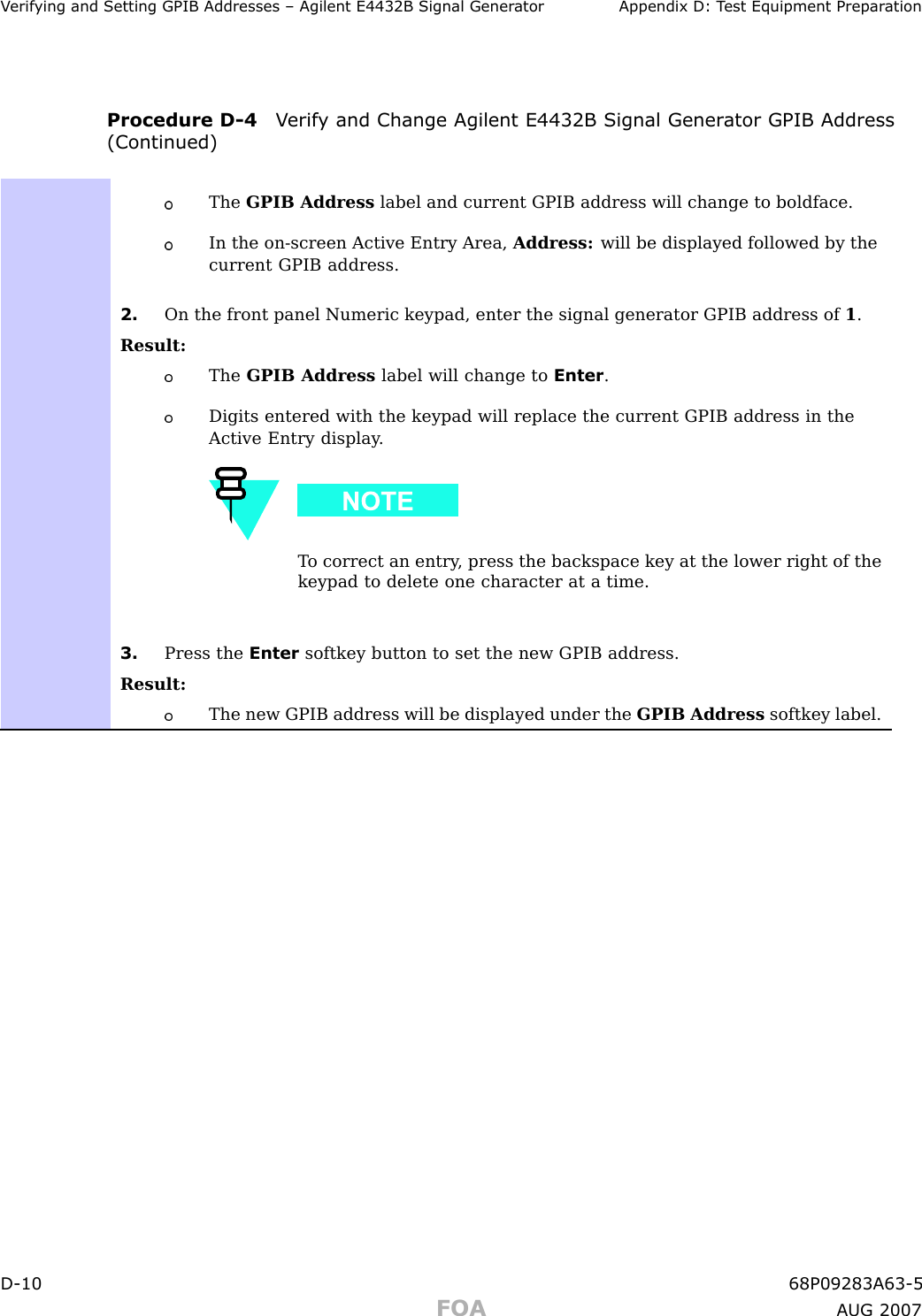
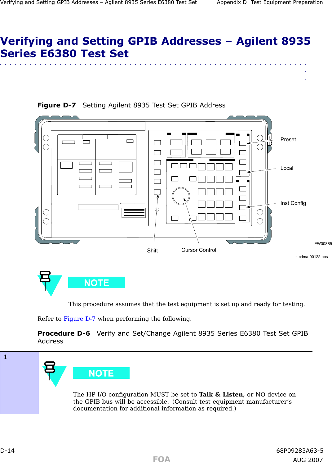
![Continuous W a v eform Mode Chapter 4: Acceptance T est ProceduresContinuous Waveform Mode■■■■■■■■■■■■■■■■■■■■■■■■■■■■■■■■■■■■■■■■■■■■■■■■■■■■■■■■■■■■■■■■ObjectiveThis test verifies that the UBS frames can generate an unmodulated carrier tone on a singlesector at any single channel number within the supported carrier frequency range of the frame.Unlock Continuous Waveform ModeW inLMF must be connected to the UBS frame to be tested and logged in.Procedure 4 -7 Procedure to Unlock Continuous W a v eform Mode1On the menu, click on UBS -> Unlock Continuous W aveform Mode2Click the Y es button in the confirmation dialog box.3A status report window will appear that shows the result of the action request.WinLMF will fail to set up Continuous W a v eform Mode for Modemdevices pro visioned in the congur ation les on DMI, but notph ysically installed in the fr ame, and for Modem devices under reset.4Select tested Sector/Carrier and click Device->X CVR->K ey menu item.5In K ey window:Enter the desired power level [dBm] in the X CVR Gain boxEnter the desired channel in the X CVR Channel box6Click the OK button in K ey window .A status report window will appear that shows the result of the action request.7P erform the required testing on the selected Sector/Carrier .8Select Sector/Carrier keyed in step 4 andclick Device->X CVR->Dekey menu item.A status report window will appear that shows the result of the action request.9T o perform unmodulated carrier mode test onother Sector/Carrier repeat procedure from step 4 .If testing using unmodulated carrier mode is completed follow LockContinuous W aveform Mode Procedure4 -24 68P09283A63 -5FOA A UG 2007](https://usermanual.wiki/Nokia-Solutions-and-Networks/T5JX1.Exhibit-8f/User-Guide-1056993-Page-9.png)
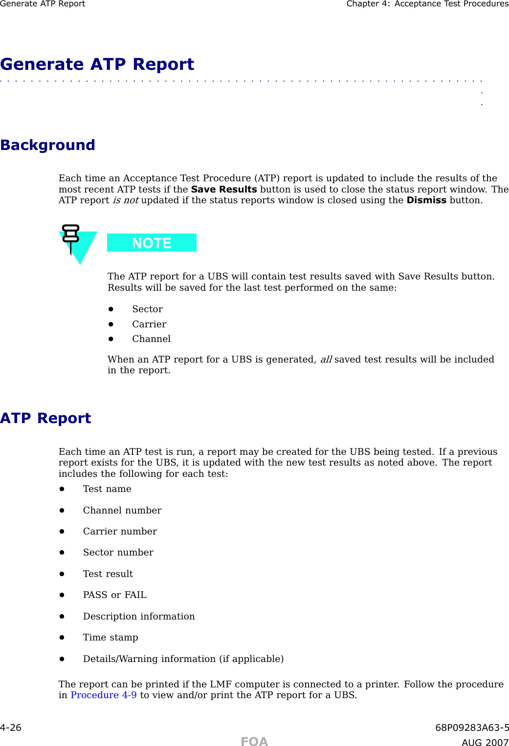


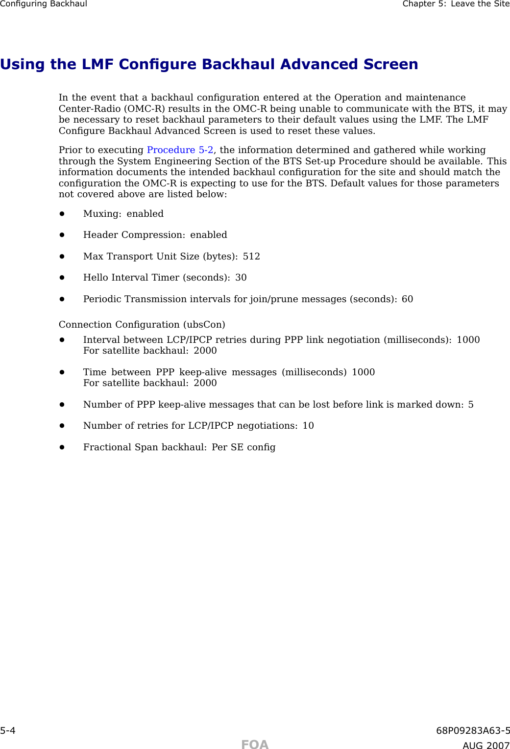


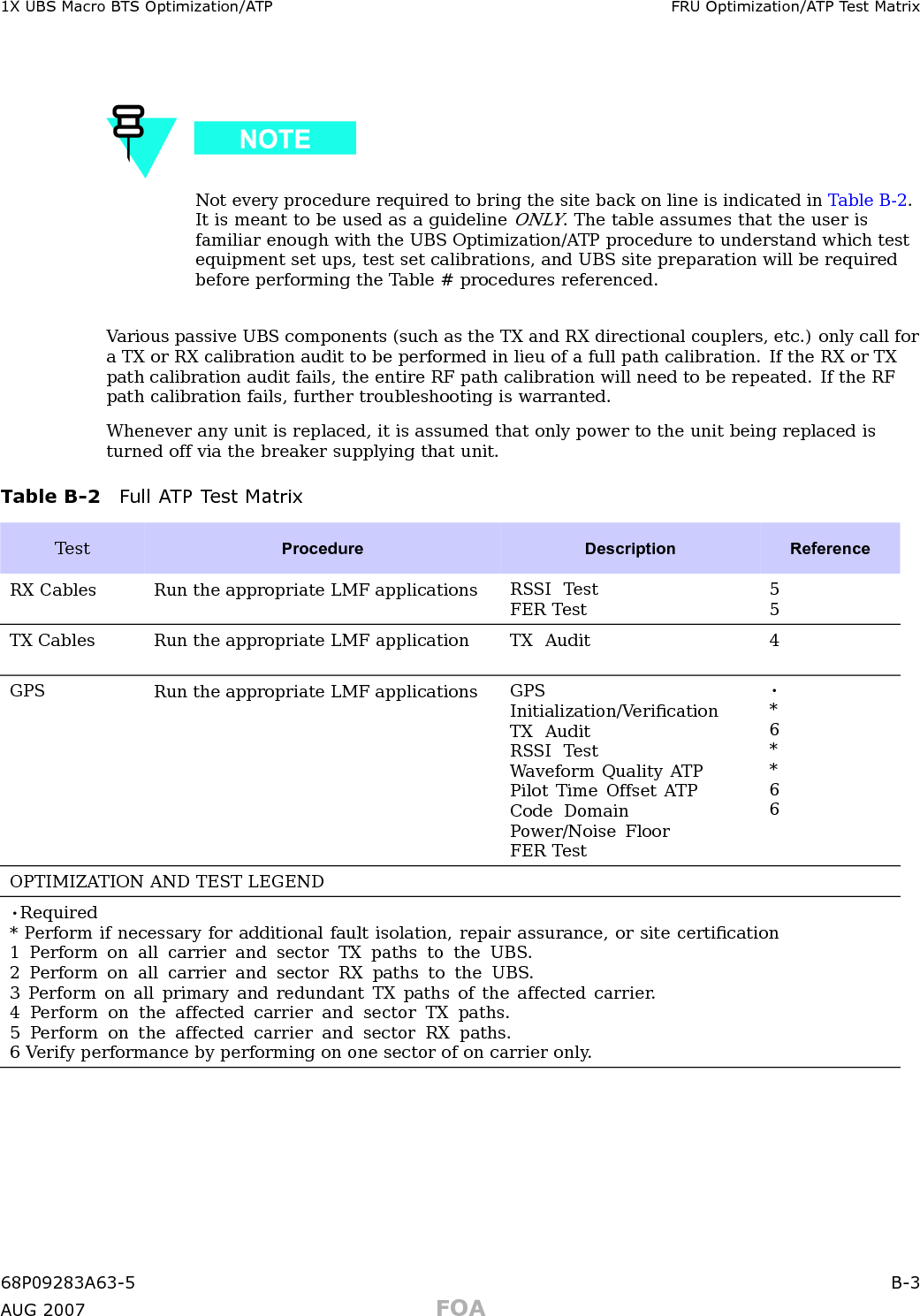

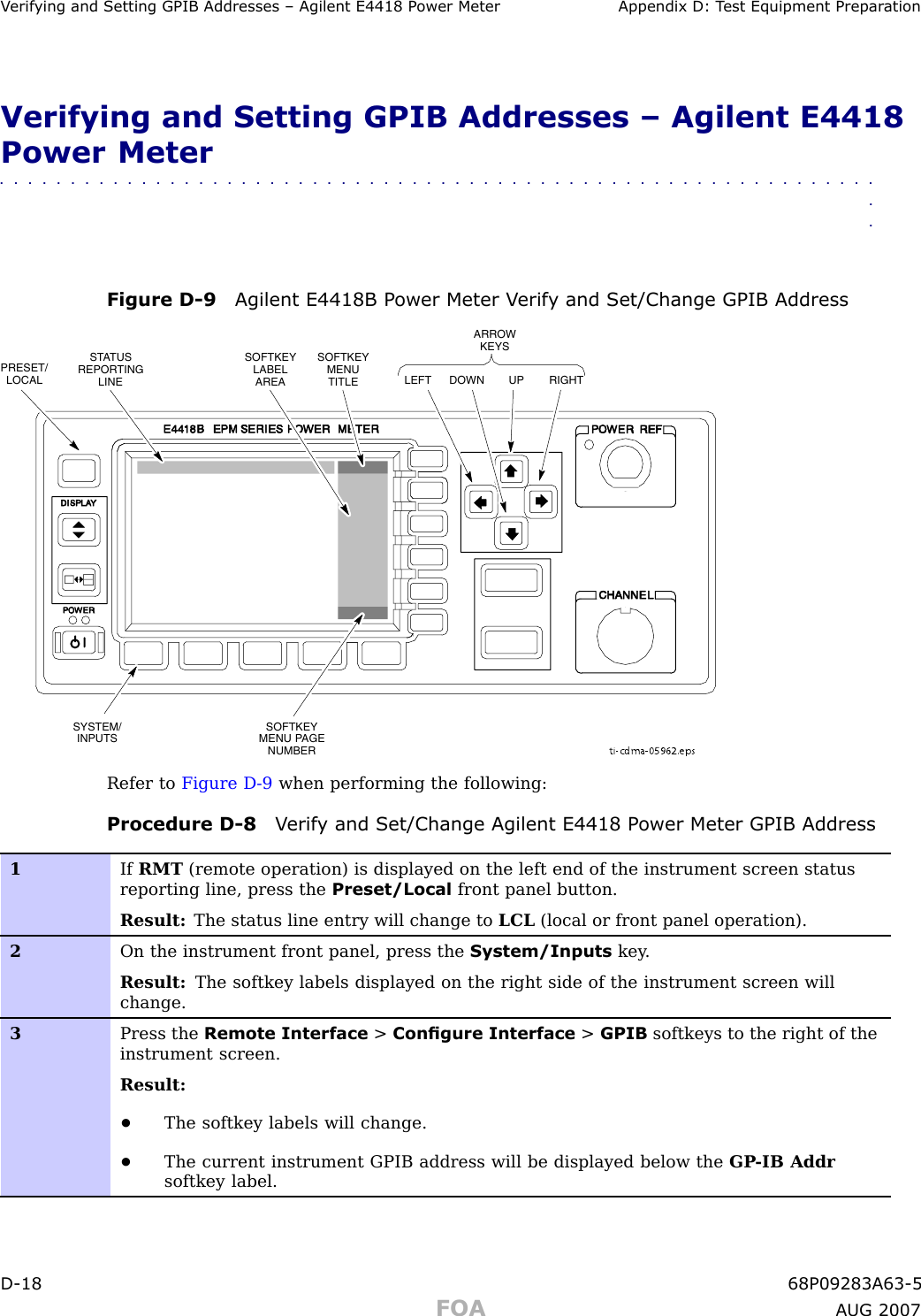
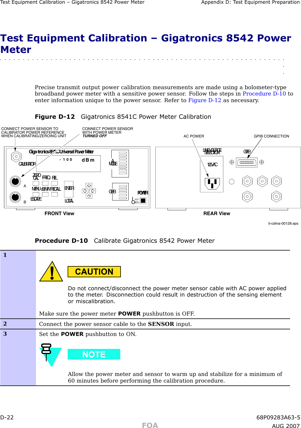
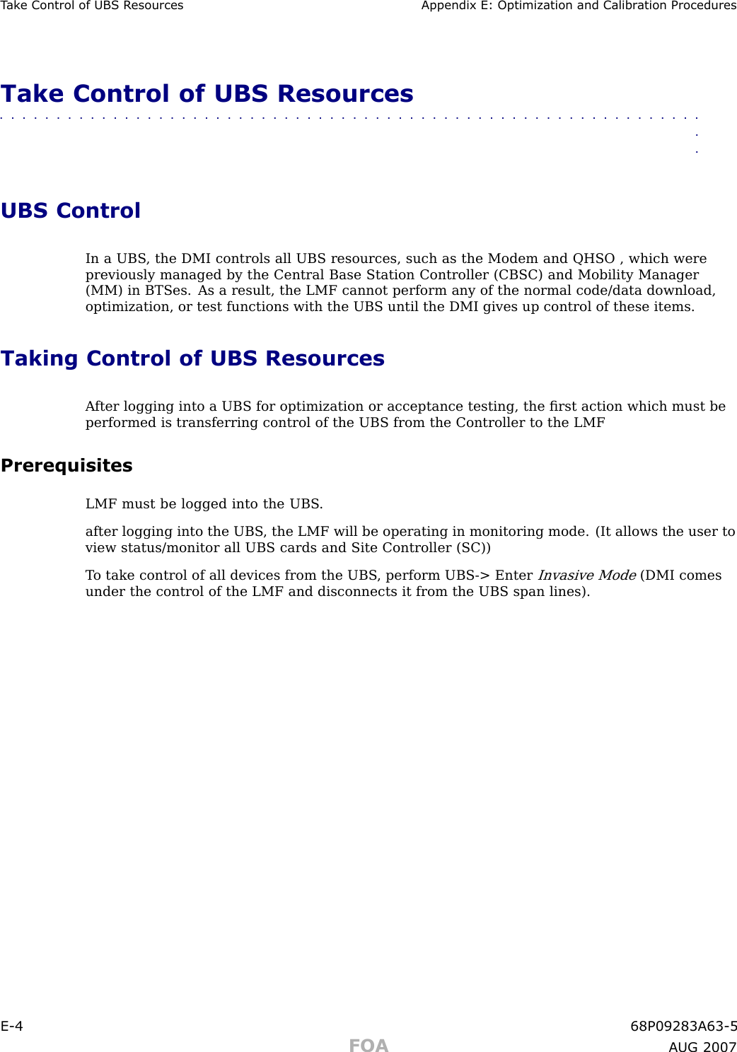
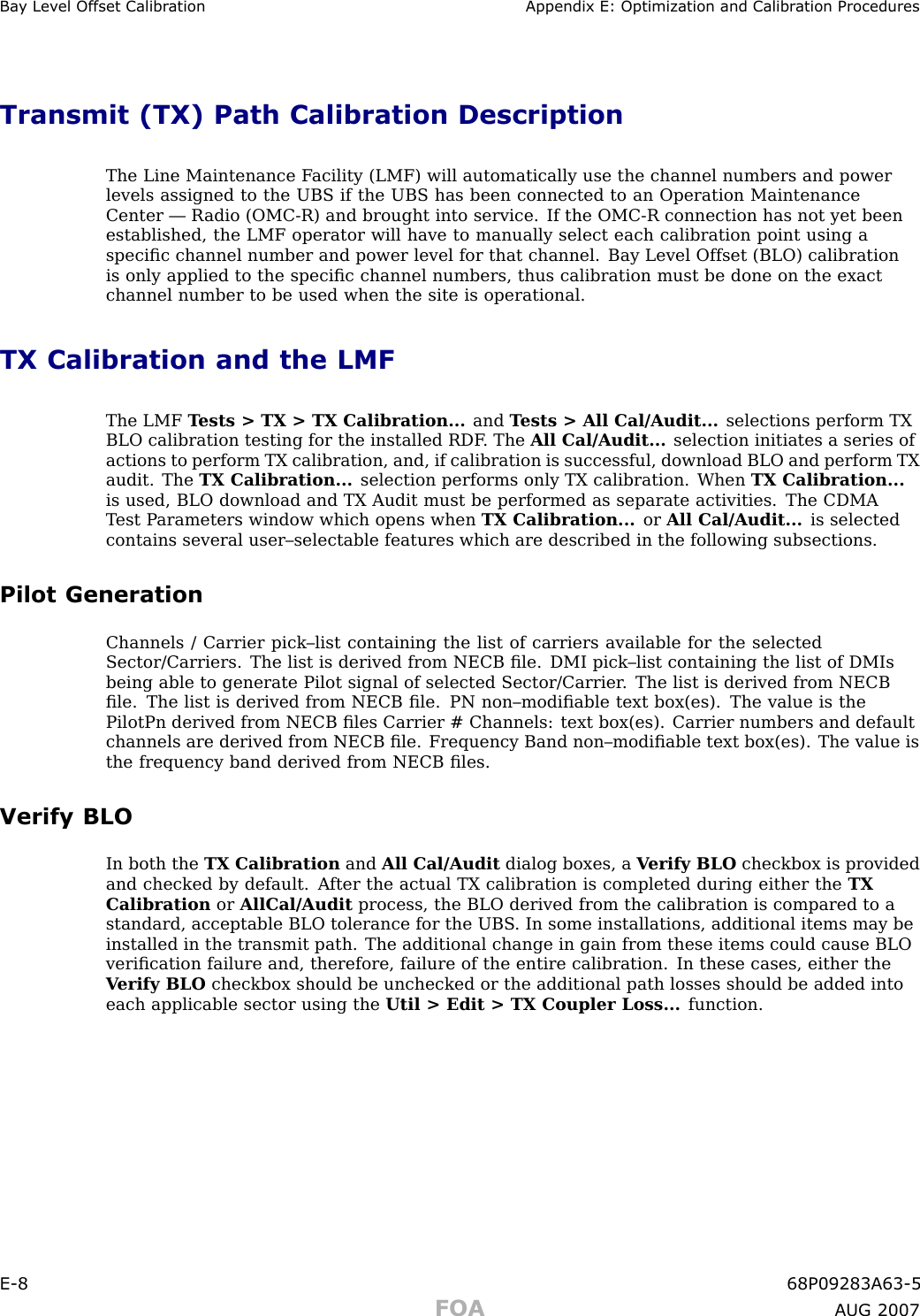
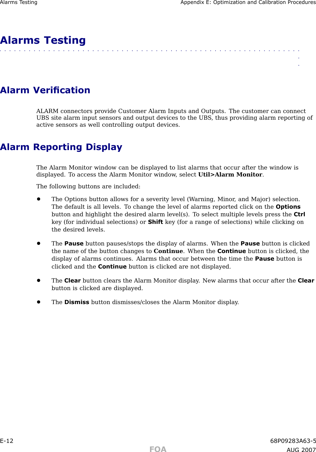
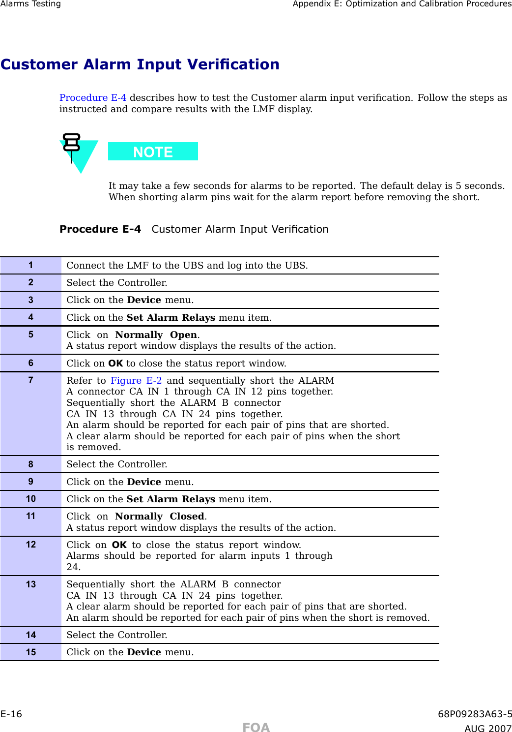
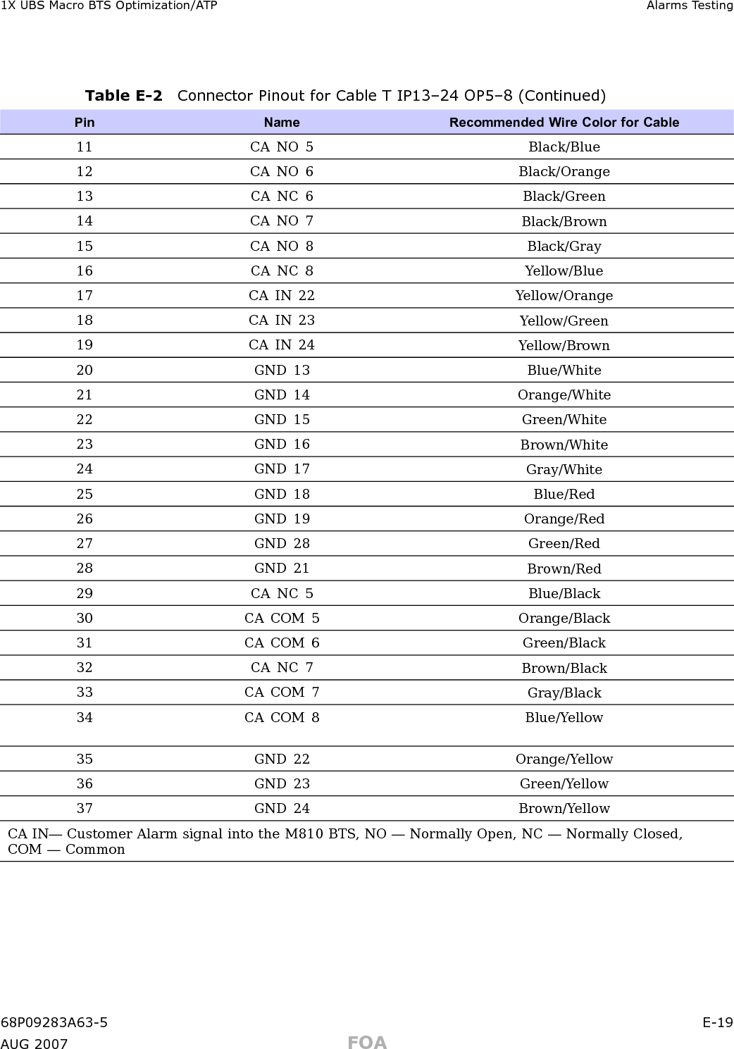
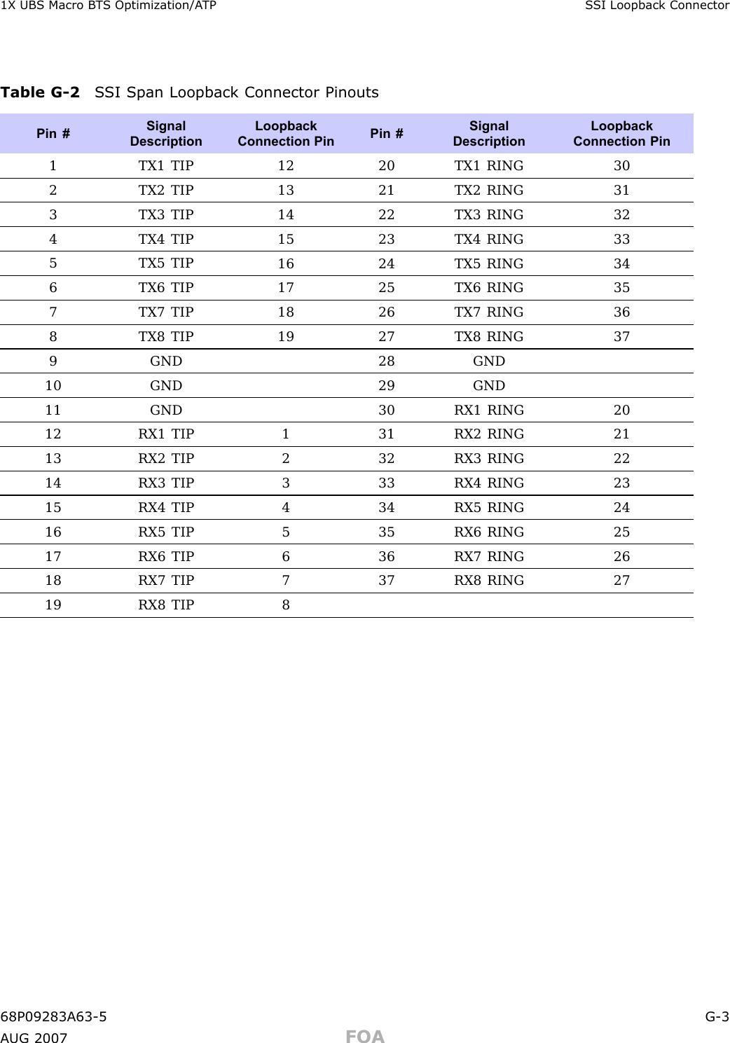
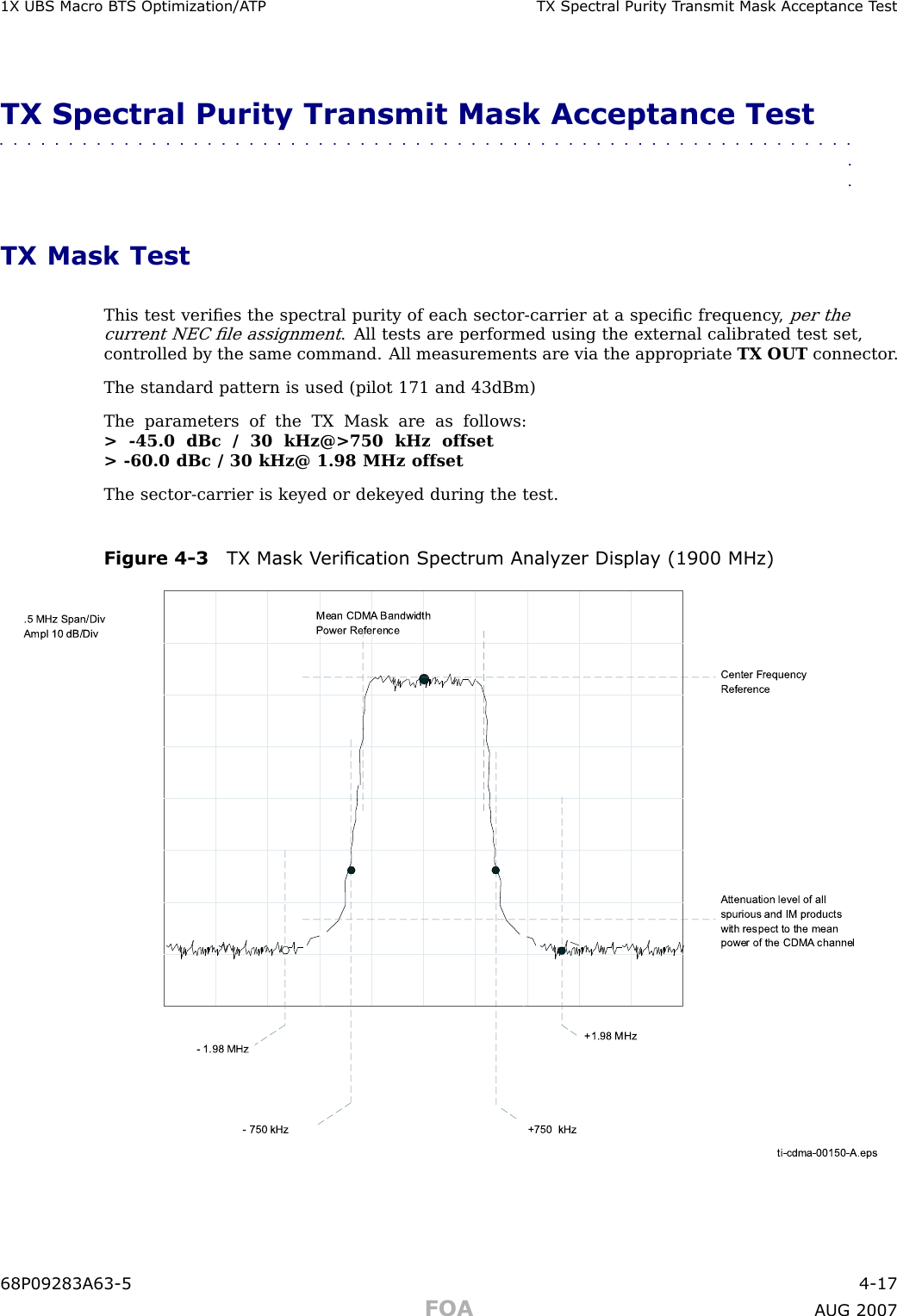
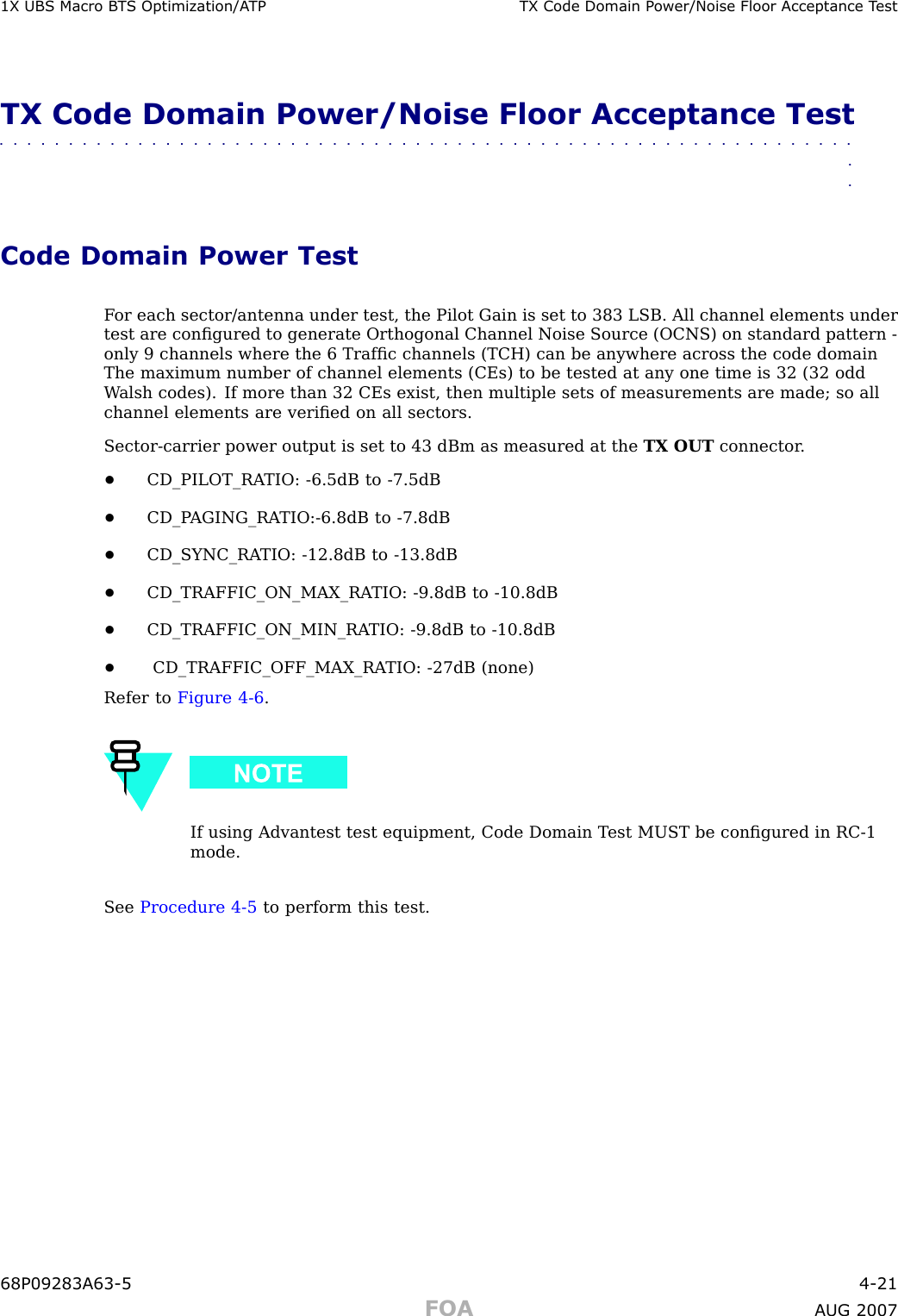
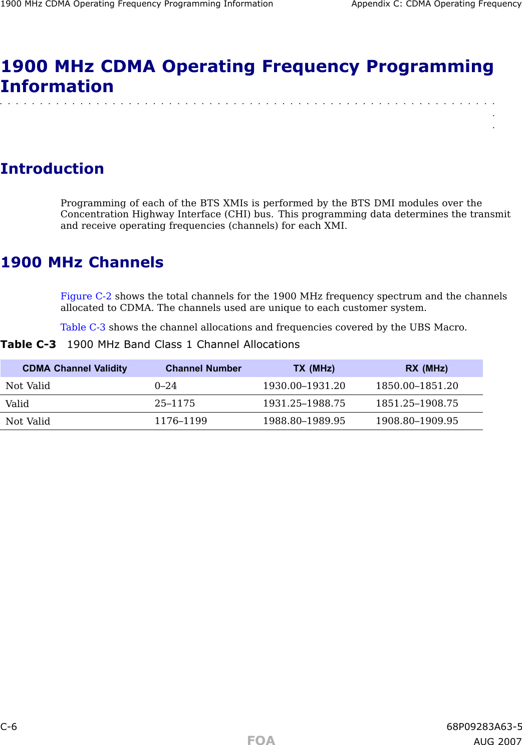
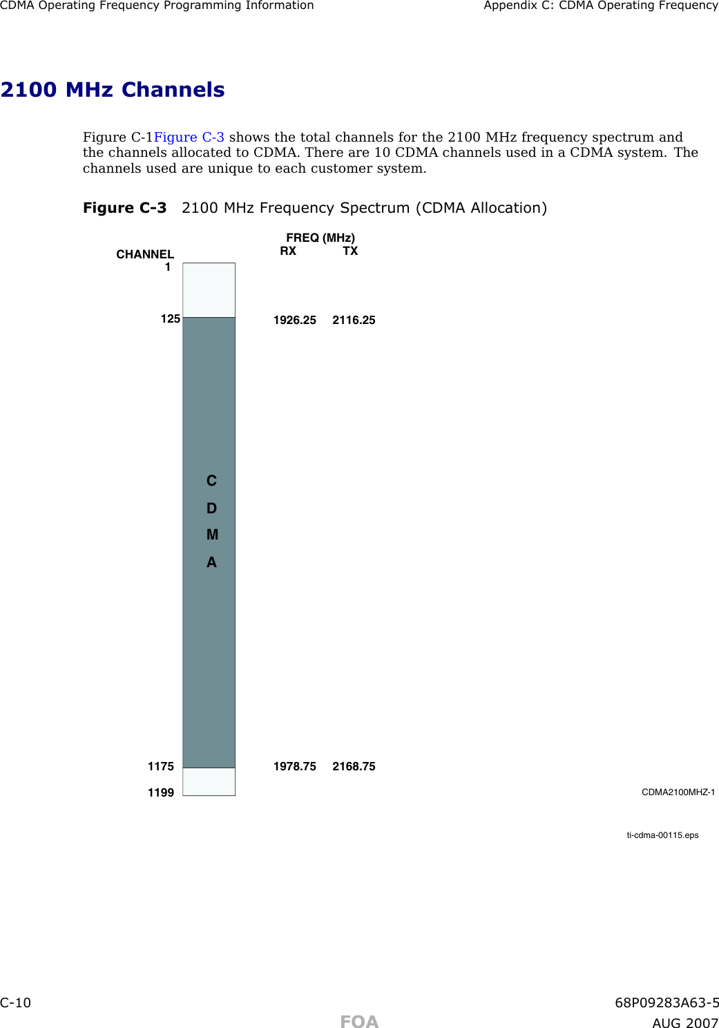
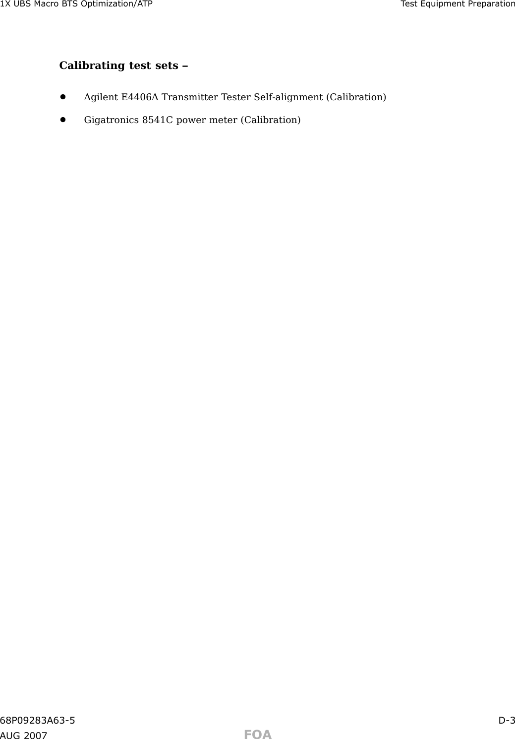
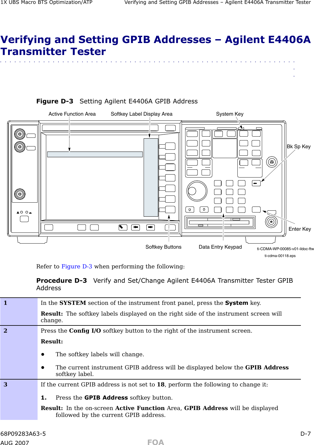
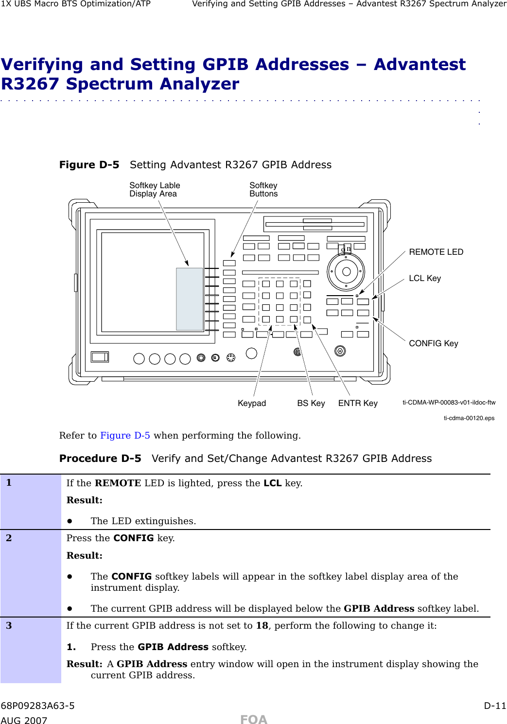
![1X UBS Macro B T S Optimization/A TP 800 MHz CDMA Oper ating Frequency Progr amming Information800 MHz Channel Center FrequenciesT able C -2 shows the valid 800 MHz CDMA channels, listed in both decimal and hexadecimal,and the corresponding transmit and receive frequency for each.Actual frequencies used depend on customer CDMA system frequency plan.Other channels and frequencies can be calculated using the following formula:F or channels 1–799:•TX Freq = 870.00 + (0.03 x Channel)•RX Freq = (0.03 x Channel) + 825.00F or channels 991–1023:•TX Freq = 870.00 + [0.03 x (Channel - 1023)]•RX Freq = [0.030 x (Channel - 1023)] + 825.00F or channels 1024–1323:•TX Freq = 860.04 + [0.03 x (Channel - 1024)]•RX Freq = [0.030 x (Channel - 1024)] + 815.04F or channels 1324–1490:•TX Freq = 860.04 + [0.03 x (Channel - 1024)]•RX Freq = [0.030 x (Channel - 1024)] + 815.04Table C -2 800 MHz TX and RX Channel Center FrequenciesDecimal HexT ransmit Center Frequency (MHz) Receive Center Frequency (MHz)1021 03FD 869.94 824.941023 03FF 870.00 825.001 0001 870.03 825.03303 012F 879.09 834.09364 016C 880.92 835.92636 027C 889.32 844.32666 029A 889.99 844.35716 02CC 891.49 844.98747 02EB 893.10 847.71769 0301 893.31 848.0768P09283A63 -5 C -5A UG 2007 FOA](https://usermanual.wiki/Nokia-Solutions-and-Networks/T5JX1.Exhibit-8f/User-Guide-1056993-Page-34.png)
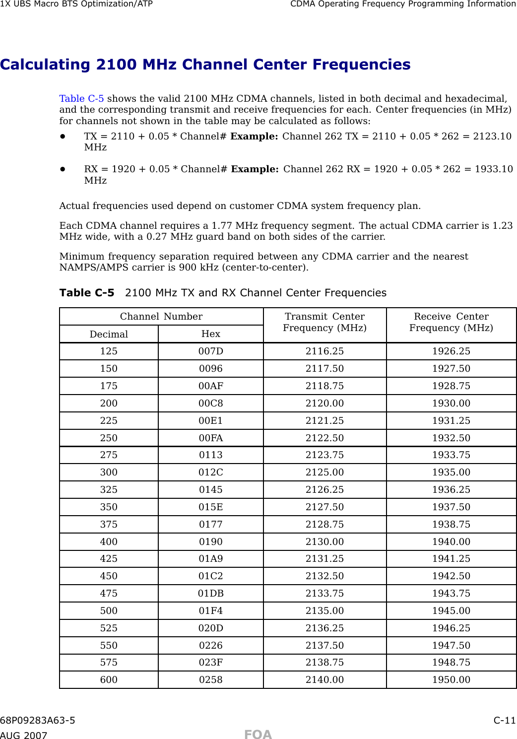

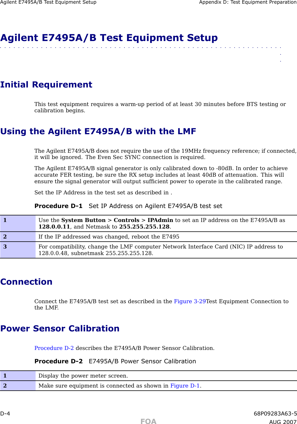
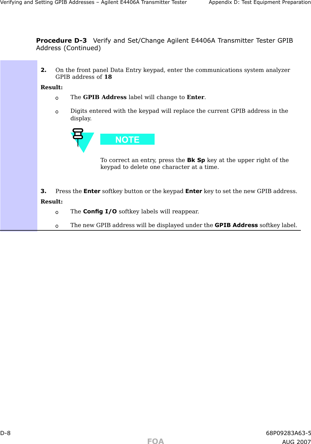
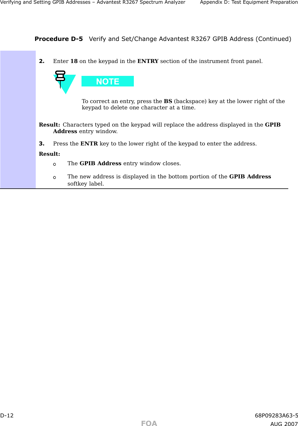
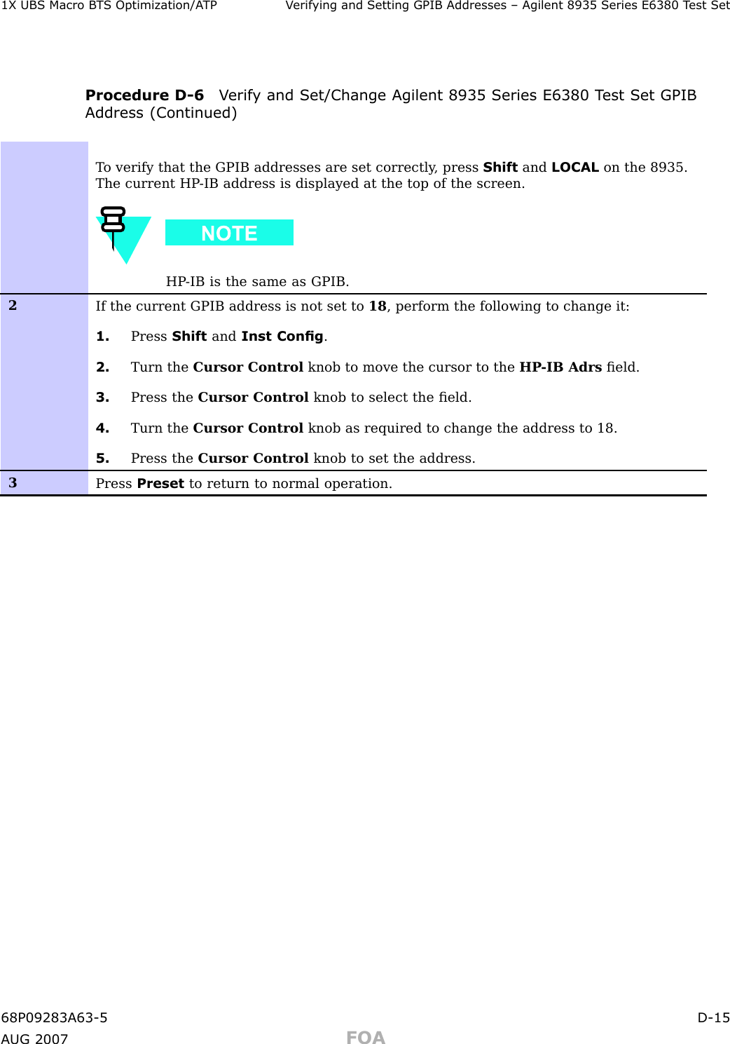
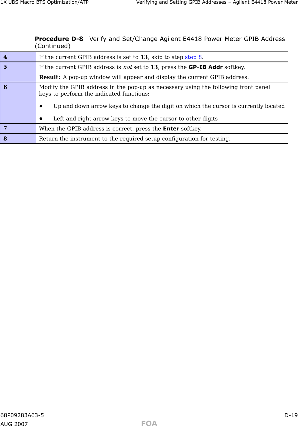
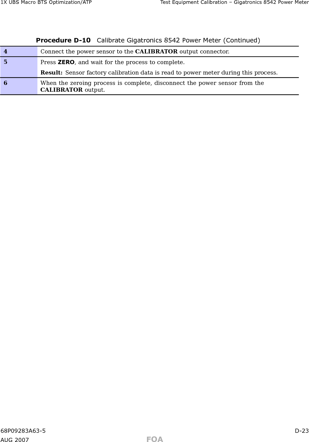
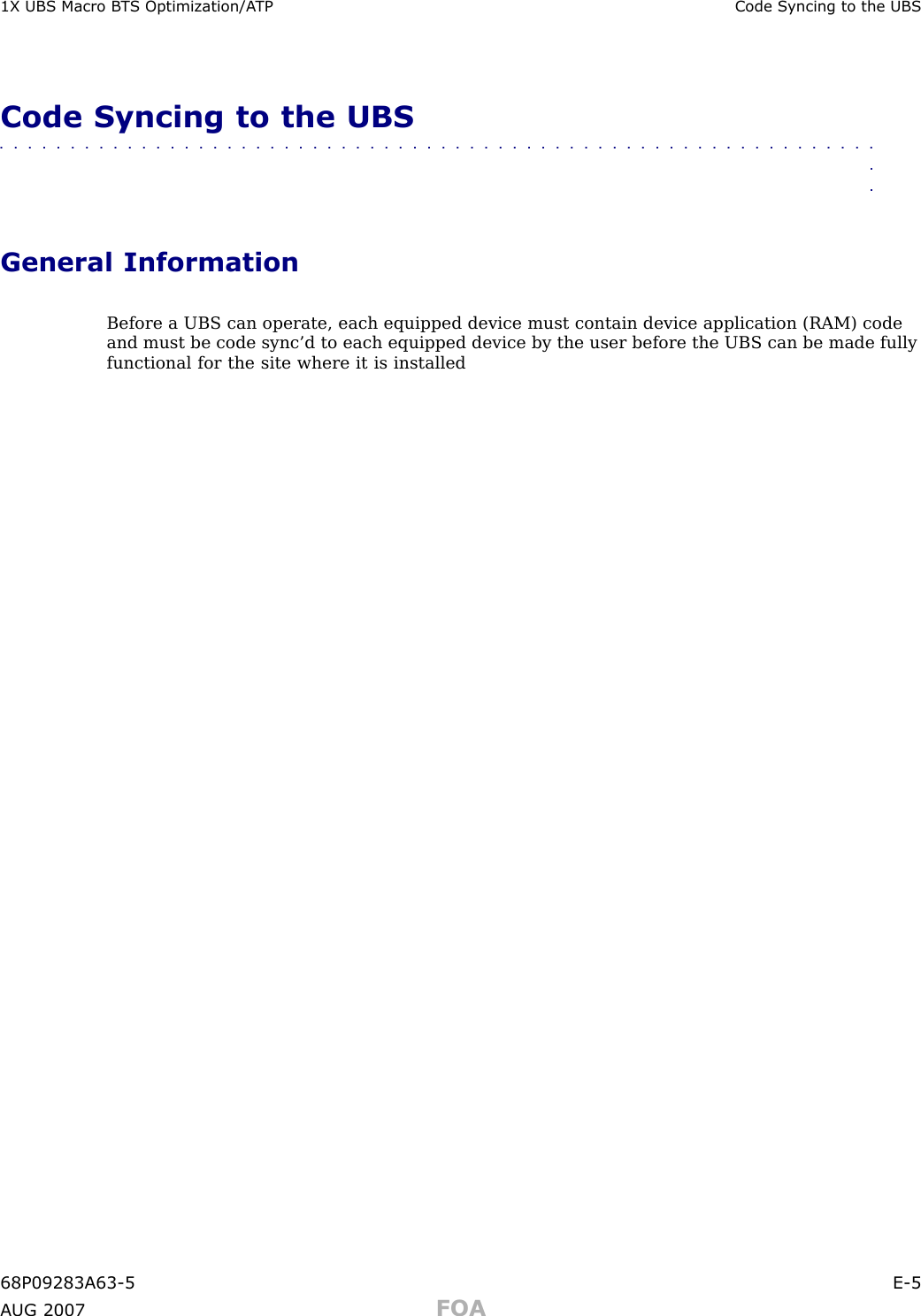
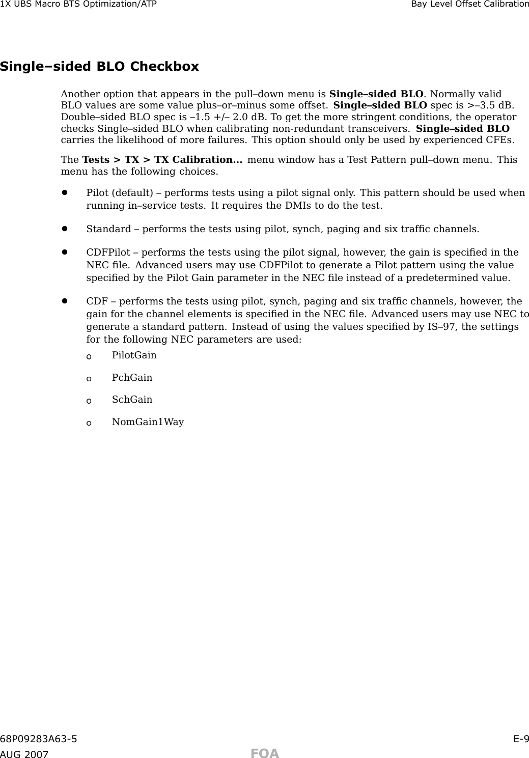
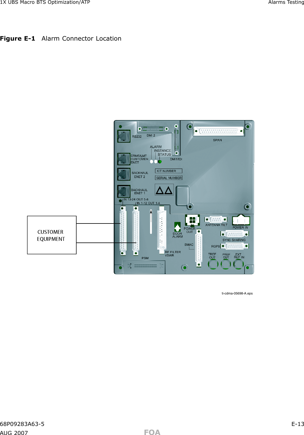
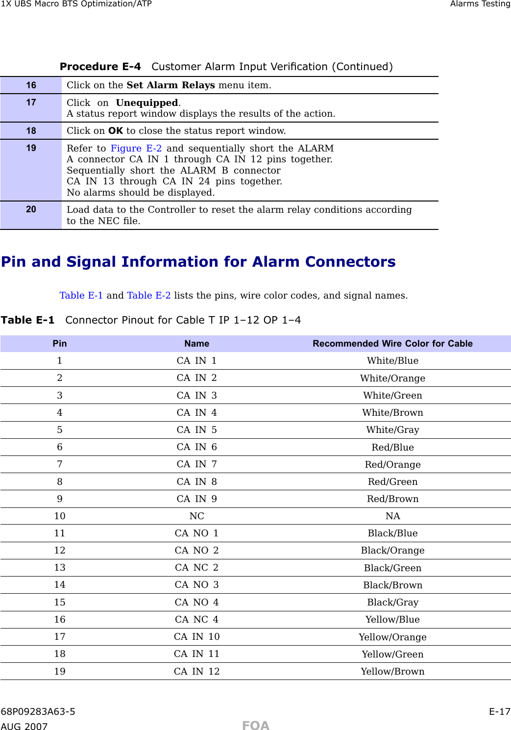
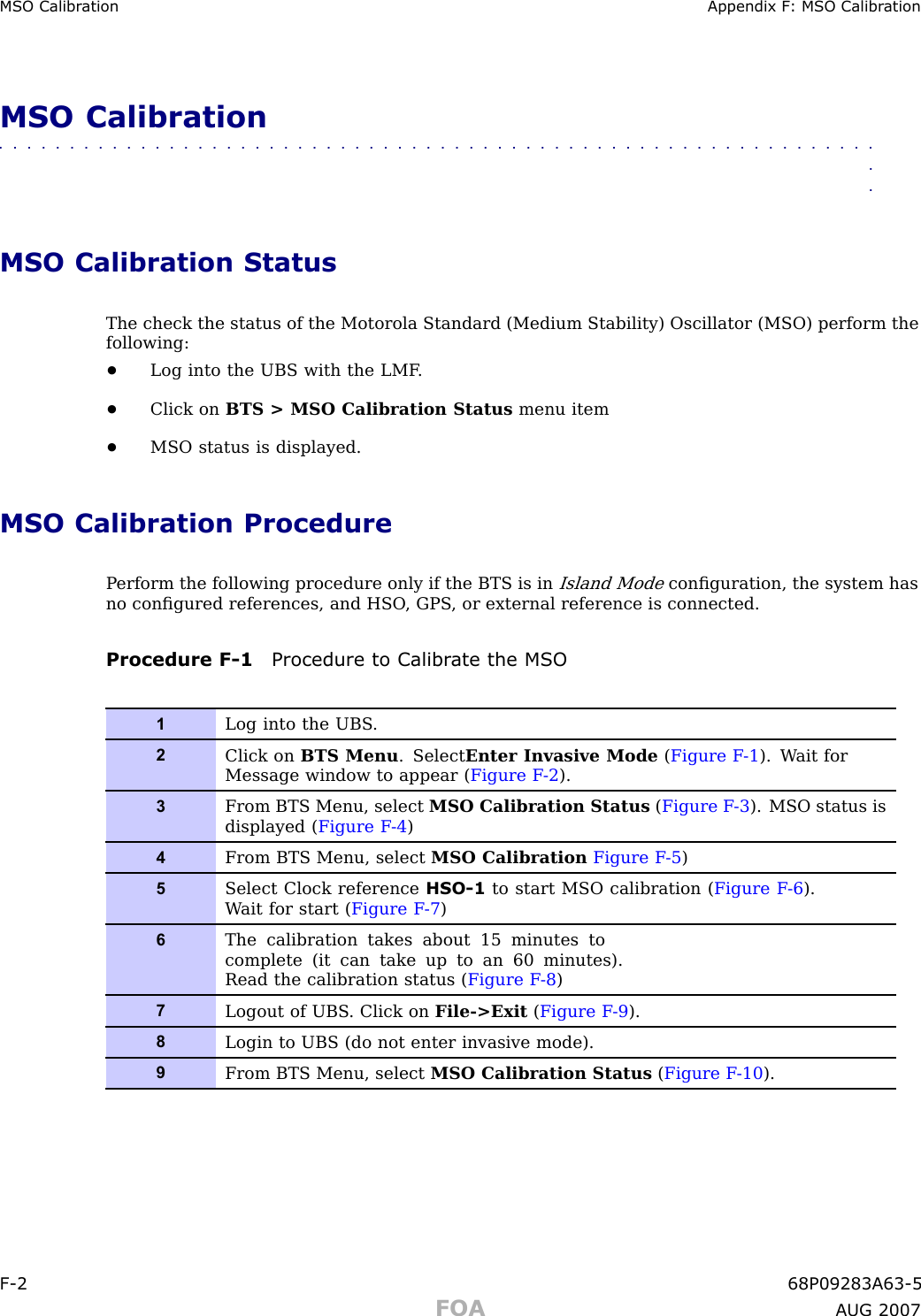
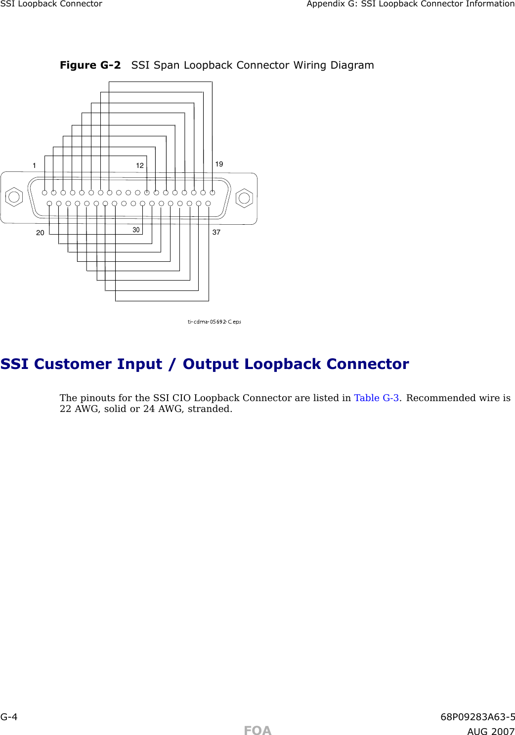
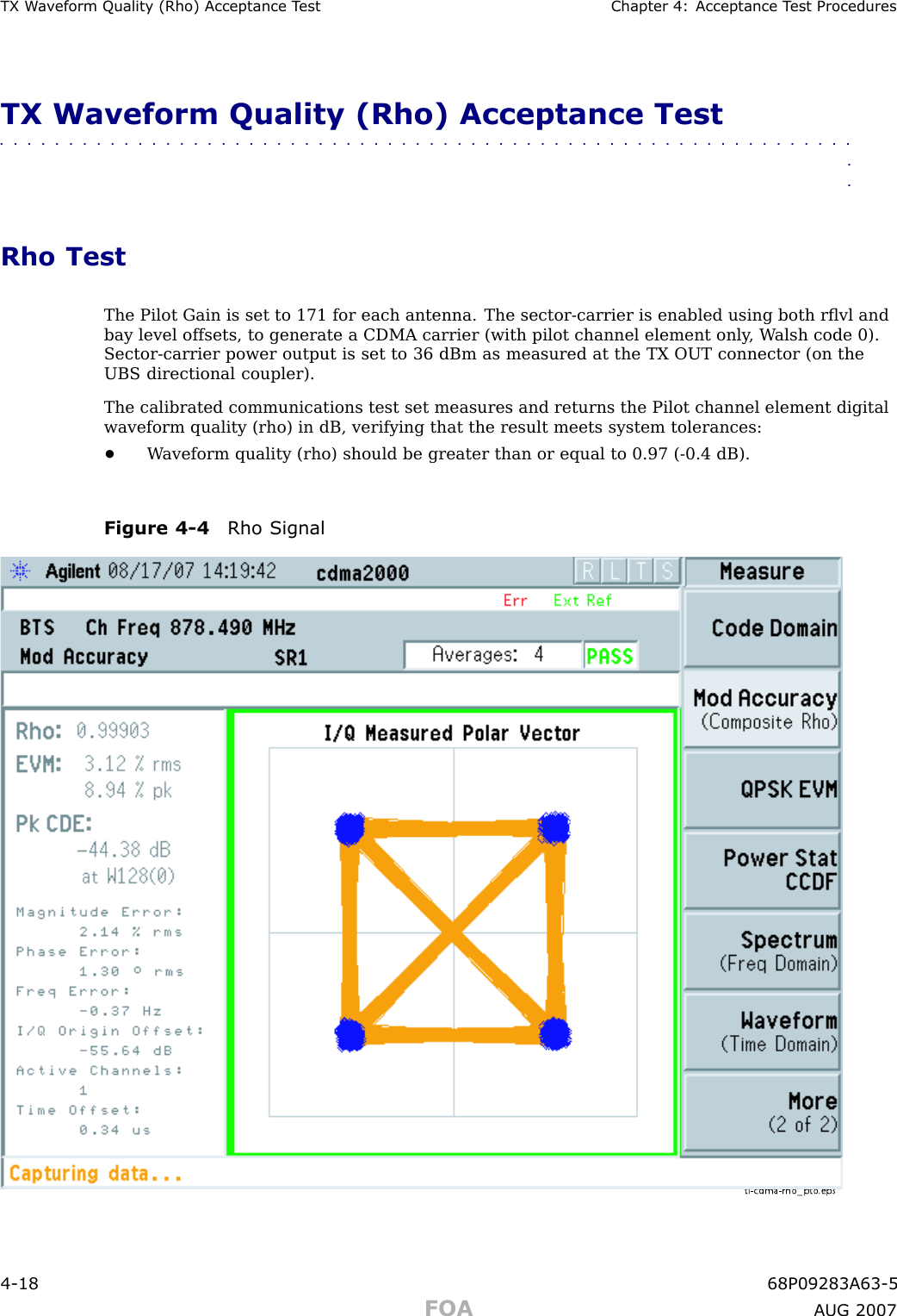
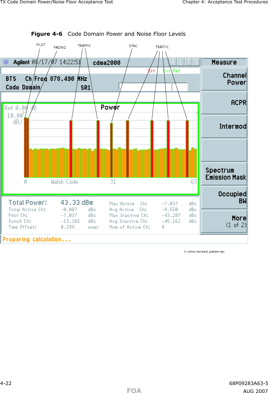
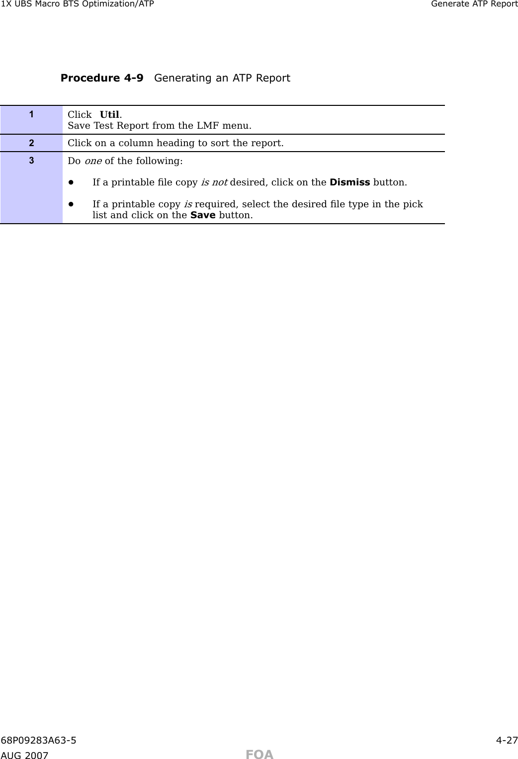
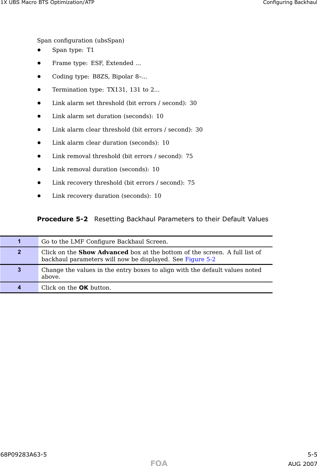
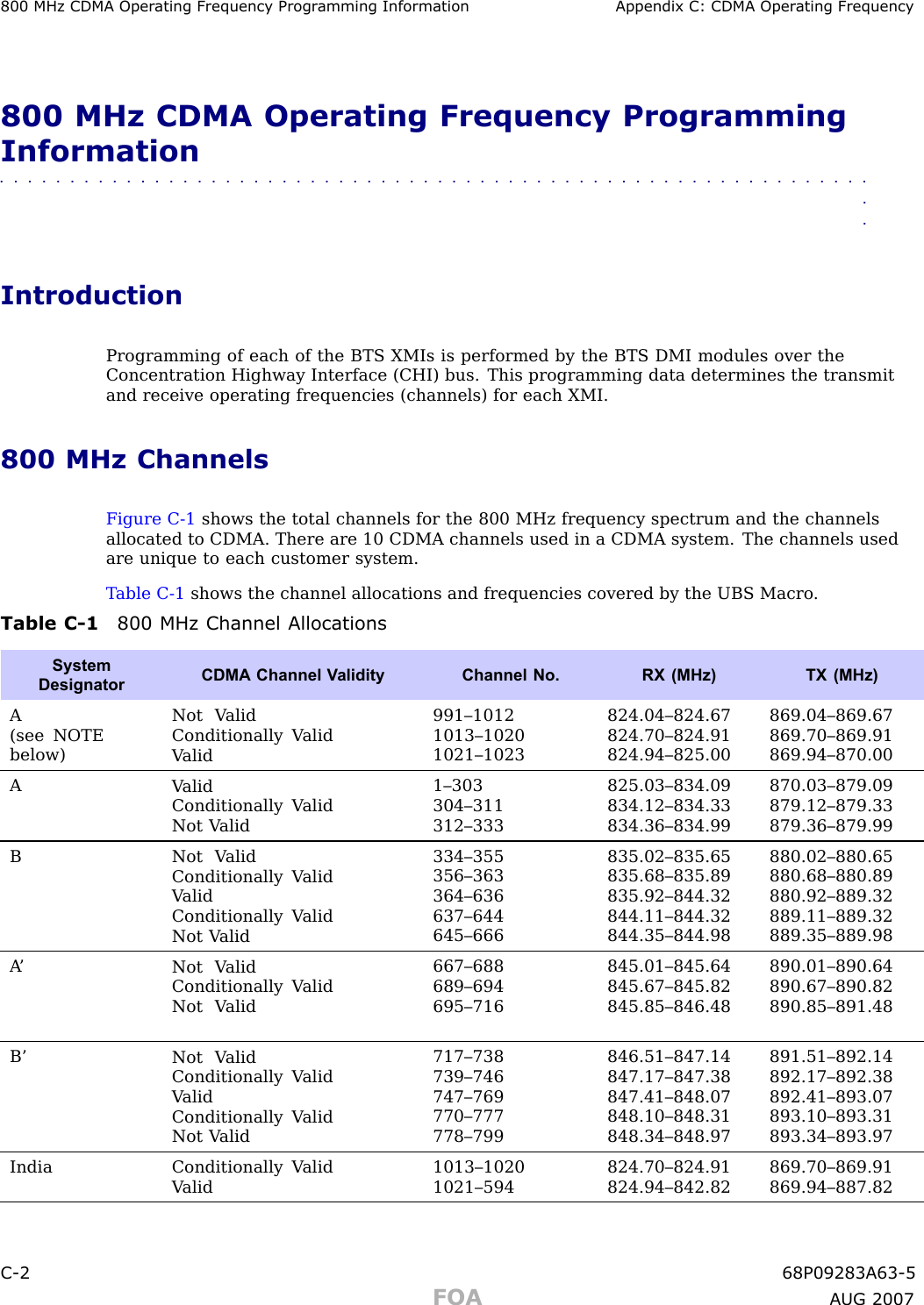
![V erif ying and Setting GPIB Addresses – Gigatronics 8541C P ower Meter Appendix D: T est Equipment Prepar ationVerifying and Setting GPIB Addresses – Gigatronics8541C Power Meter■■■■■■■■■■■■■■■■■■■■■■■■■■■■■■■■■■■■■■■■■■■■■■■■■■■■■■■■■■■■■■■■Figure D -8 Gigatronics 8541C P ower Meter Detailti-cdma-00128.epsCONNECT POWER SENSOR WITH POWER METER TURNED OFFCONNECT POWER SENSOR TO CALIBRATOR POWER REFERENCE WHEN CALIBRATING/ZEROING UNITCALIBRATORZEROCAL FREQRELMENUESCAPEdB/MWRECALLLOCALENTERAMODEGPIBPOWERIOGiga-tronics8542CUniversalPowerMeterdB m- 1 0 0LINEVOLTAGESELECTION GPIB120VACFRONT View REAR ViewGPIB CONNECTIONAC POWERABRefer to Figure D -8 when performing the following:This procedure assumes that the test equipment is set up and ready for testing.Procedure D -7 V erif y and Set/Change Gigatronics 8541C P ower Meter GPIB Address1Do not connect/disconnect the power meter sensor cable with AC power appliedto the meter . Disconnection could result in destruction of the sensing elementor miscalibr ation.Press MENU .2Use the [Symbol_arrowblackdown] arrow key to select CONFIG MENU and press ENTER .3Use the [Symbol_arrowblackdown] arrow key to select GPIB and press ENTER .Result: The current Mode and GPIB Address are displayed.D -16 68P09283A63 -5FOA A UG 2007](https://usermanual.wiki/Nokia-Solutions-and-Networks/T5JX1.Exhibit-8f/User-Guide-1056993-Page-57.png)