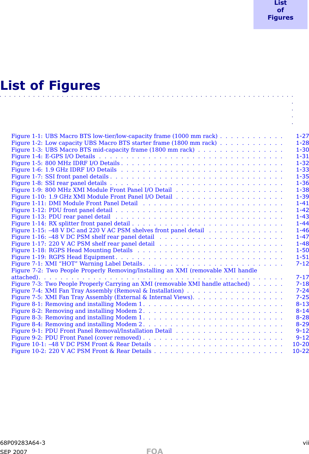
Nokia Solutions and Networks T5JX1 UBS CDMA XMI Transceiver at 800 MHz User Manual Exhibit 8b
Nokia Solutions and Networks UBS CDMA XMI Transceiver at 800 MHz Exhibit 8b
UserManual.wiki
>
Nokia Solutions and Networks
>
T5JX1 User Manual
>
Exhibit 8b
Contents
1.
Exhibit 8a
2.
Exhibit 8b
3.
Exhibit 8c
4.
Exhibit 8d
5.
Exhibit 8e
6.
Exhibit 8f
Exhibit 8b
Navigation menu
Upload a User Manual
Namespaces
Wiki Guide
HTML
PDF
Info
Views
User Manual
Discussion / Help
Navigation


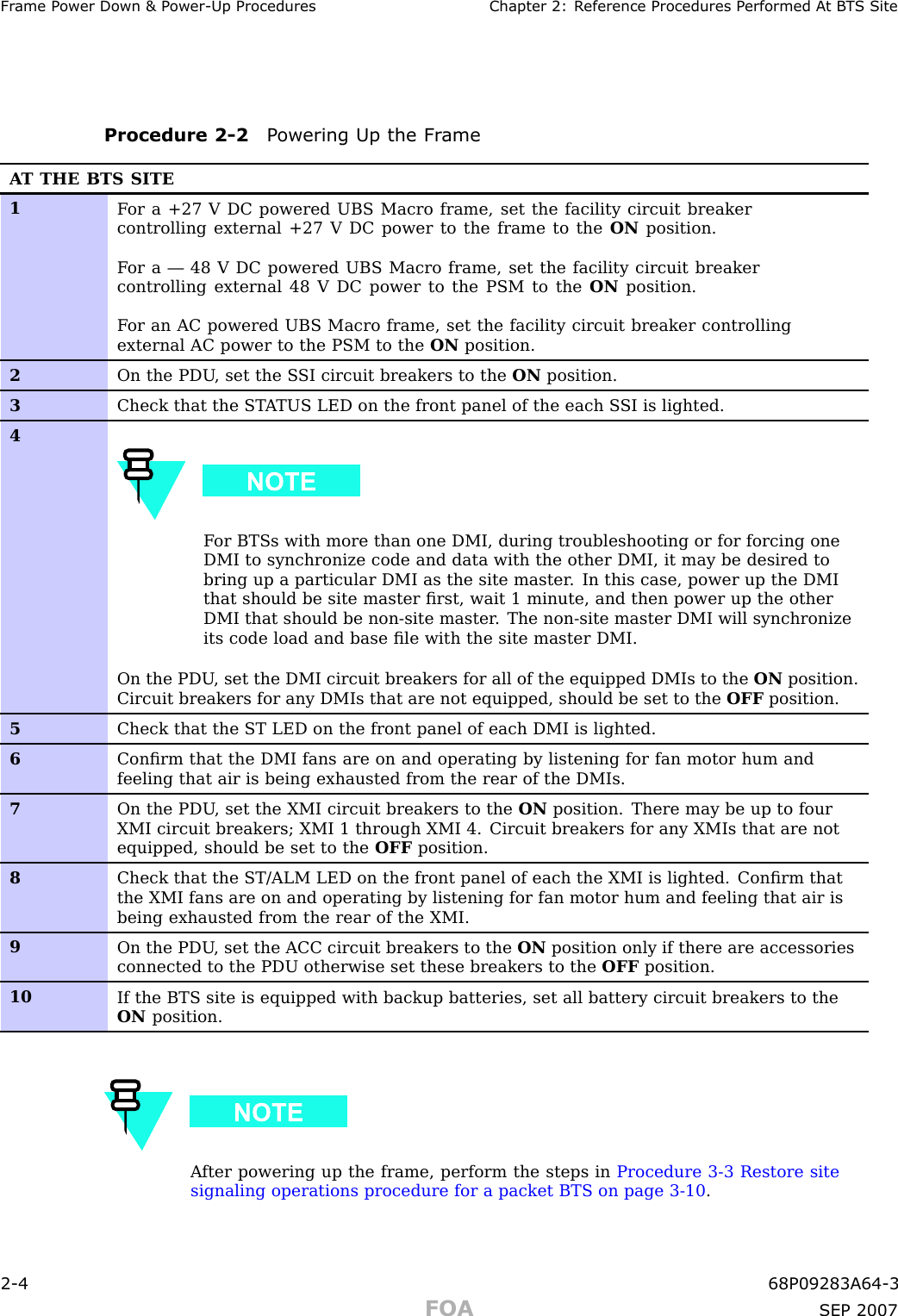
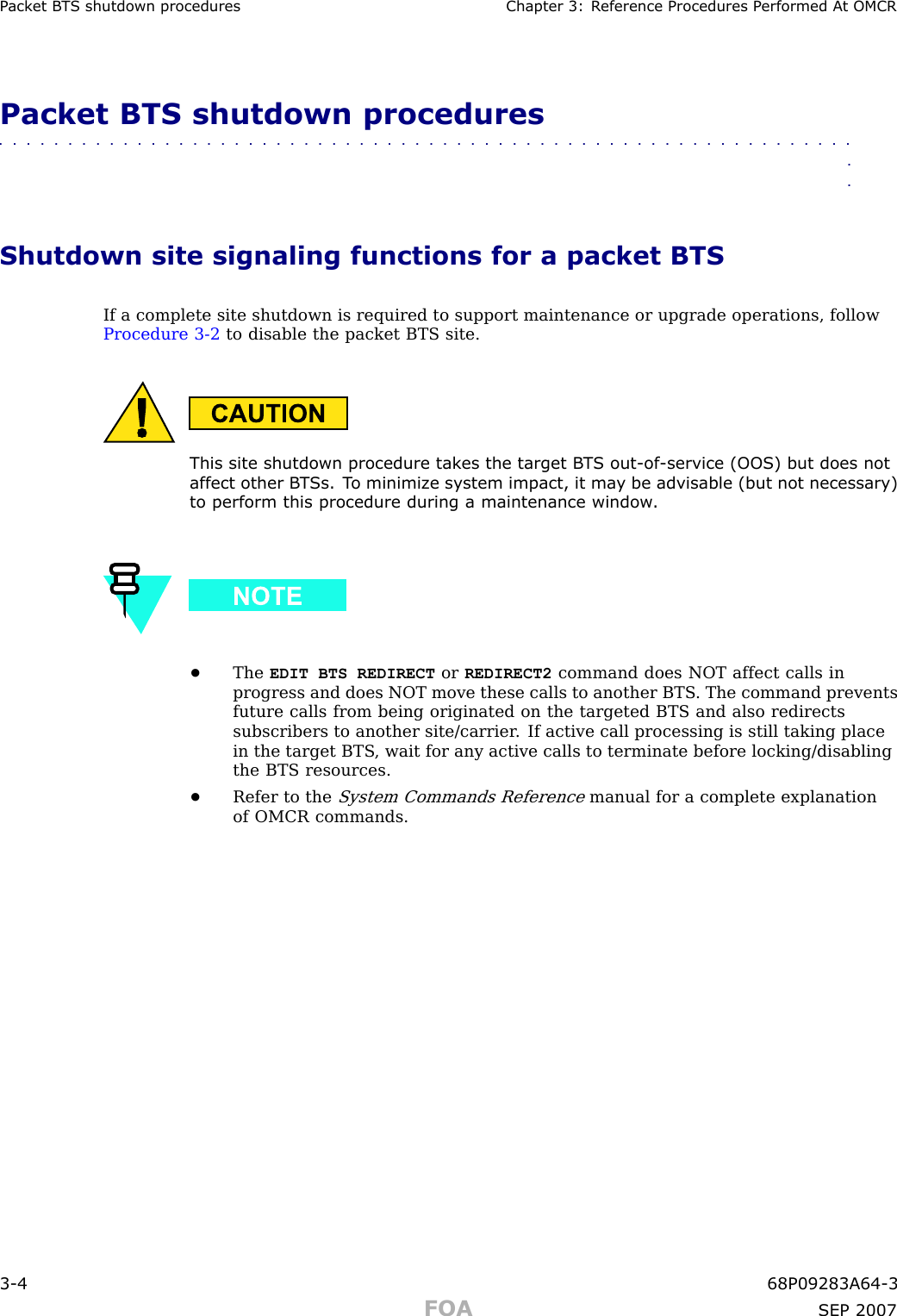
![1X UBS Macro B T S FRU P ack et B T S shutdown proceduresProcedure 3 -2 Shutdown site signaling functions procedure for a pack et B T S(Continued)6A fter all parameters are entered, the system displays the command tobe sent and the prompt below . V erify the command syntax is correct.omc-000000>Accept [yes/no]?7A t the prompt shown in step 6 , enter Yto accept the command or Nto go bottom and enterthe correct value(s).8Enter the following command at the prompt to display the status of the signaling REDIRECTparameters to verify that the applicable BTS is ready for global redirect:omc-000000> DISPLAY BTS-<bts#> REDIRECT9Ensure that the values in the system display response match the values input in step 5 .10Enter the following command at the prompt to display the status of the BTS signaling redirectparameters for all carriers equipped for the BTS:omc-000000> DISPLAY BTS-<bts#> REDIRECT21 1Record the values shown in the system display response resulting from step 10 .These values are used to answer the prompts for the EDIT BTS REDIRECT2command when restoring signaling operations at the end of the replacementprocedure.12This step edits the REDIRECT2 parameters so that the Global Service RedirectMessage to be broadcast on the paging channel redirects all subscribers away fromthe BTS with the failed equipment and onto a CDMA channel at a neighbor site.Enter the following command at the prompt:omc-000000> EDIT BTS-<bts#> REDIRECT2!The system prompts to enter each command parameter value one at a time. Answer theprompts in the following order:expecting an integer number (from 0 to 65535)<EXPNID= ?>Continued68P09283A64 -3 3 -7FOA SEP 2007](https://usermanual.wiki/Nokia-Solutions-and-Networks/T5JX1.Exhibit-8b/User-Guide-1056989-Page-90.png)
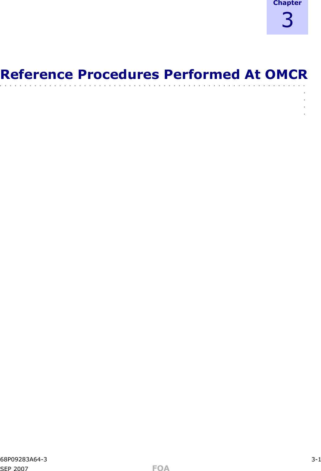
![P ack et B T S shutdown procedures Chapter 3: R eference Procedures P erformed A t OMCRProcedure 3 -2 Shutdown site signaling functions procedure for a pack et B T S(Continued)(Use the Network ID the subscriber units should expect to find on the system they arebeing redirected to .)expecting an integer number (from 0 to 2047)<chan1= ?>, <chan2= ?> . . . <chan15= ?>(A list of CDMA channels for neighbor sites that the subscriber units can use for redirection.)expecting an enumerated value:CDMA1900 CDMA2100 CDMA800 CDMA900 JAPANCDMA<BANDCLASS= ?>(Use CDMA1900 for 1900 MHz systems, CDMA2100 for 2100 MHz systems, and CDMA800for 800 MHz systems. This example uses 1900 MHz.)13A fter all parameters are entered, the system displays the command to be sent and the promptbelow . V erify the command syntax is correct.omc-000000>Accept [yes/no]14A t the prompt shown in step 13 , enter Yto accept the command or Nto go bottom andenter the correct value(s).15Enter the following command at the prompt to display the status of the BTS signalingREDIRECT2 parameters to verify that the BTS is ready for maintenance:omc-000000> DISPLAY BTS-<bts#> REDIRECT216Ensure that the values in the system display response match the values input in step 12 .17Enter the following command at the prompt to display the existing congestion controlparameters for all carriers equipped for the BTS:omc-000000> DISPLAY BTS-<bts#> CONGESTCONF18This step edits the value of the Global Service Redirection Flag ( GLOBALREDIRECT )in the congestion control parameters so that the Global Service Redirect Messageis broadcast on all of the sector paging channels at the BTS .Enter the following command at the prompt using the applicable BTS number:omc-000000> EDIT BTS-<bts#> CONGESTCONF!Continued3 -8 68P09283A64 -3FOA SEP 2007](https://usermanual.wiki/Nokia-Solutions-and-Networks/T5JX1.Exhibit-8b/User-Guide-1056989-Page-91.png)
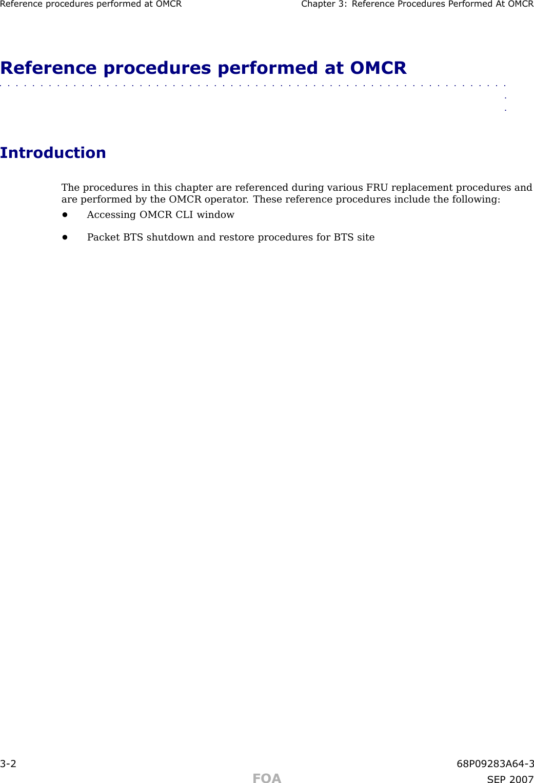
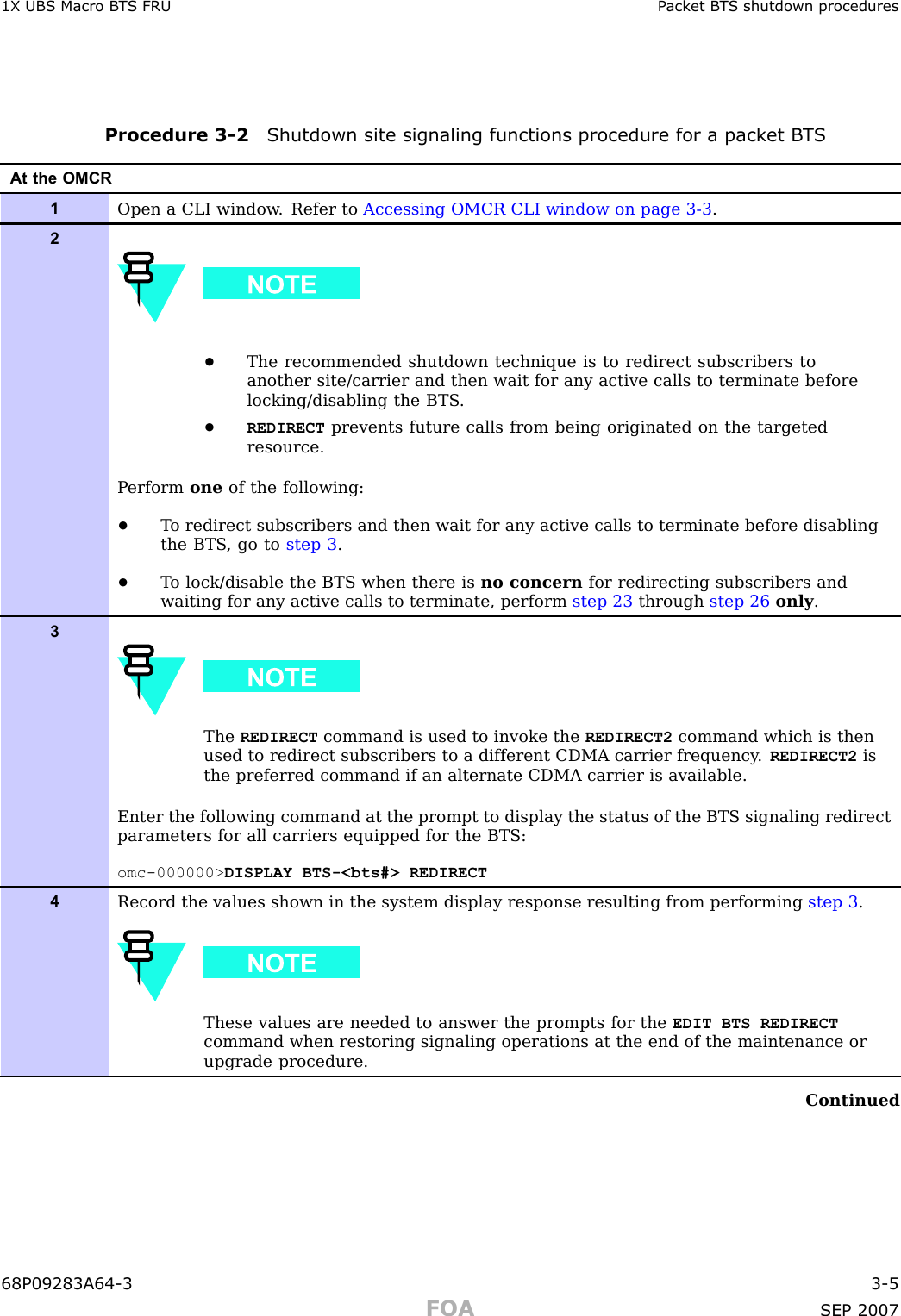
![1X UBS Macro B T S FRU P ack et B T S shutdown proceduresProcedure 3 -2 Shutdown site signaling functions procedure for a pack et B T S(Continued)19The system prompts to enter each control parameter value one at a time. Skip through theprompts until reaching the following, and enter the parameter shown:<globalredirect> ENABLE(This will force the Global Service Redirect Message to be broadcast on all of the sectorpaging channels at the BTS .)20When the system displays the values of the control parameters and the following prompt,verify that only the GLOBALREDIRECT value changed.omc-000000>Accept [yes/no]?21If only the GLOBALREDIRECT value changed, enter Yto accept the change.(When the change is accepted, the Global Service Redirection Message is sent over the sectorpaging channels. All subscribers are redirected away from the BTS and onto a differentsystem or CDMA carrier channel. This effectively shuts down the BTS .)22V erify that the CONGESTCONF Global Redirect is enabled for each carrier at the BTS by enteringthe following command at the prompt:omc-000000> DISPLAY BTS-<bts#> CONGESTCONF23Enter the following command at the prompt to display the status of all devices at the BTS:omc-000000> DISPLAY BTS-<bts#> STATUS24Record all devices that are listed as OOS_AUTOMATIC in the response to step 23 .This information will be used for later reference when restoring site signalingoperations.25W ait for three minutes to allow any active calls to terminate then go the next step.26Lock/disable the BTS by entering either of the following commands at the prompt:•omc-000000> DISABLE BTS-<bts#> UNC•omc-000000> LOCK BTS-<bts#>68P09283A64 -3 3 -9FOA SEP 2007](https://usermanual.wiki/Nokia-Solutions-and-Networks/T5JX1.Exhibit-8b/User-Guide-1056989-Page-92.png)
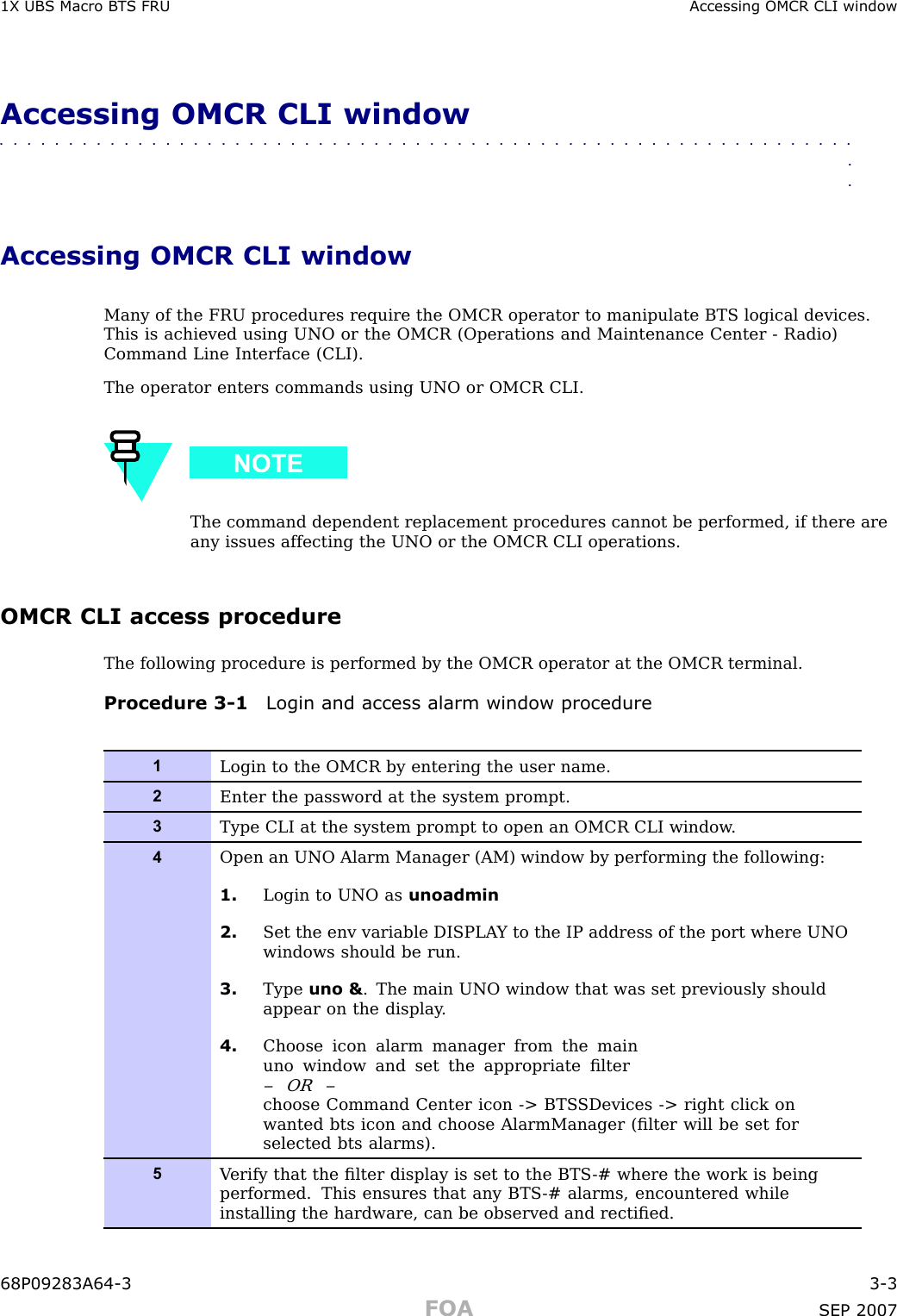
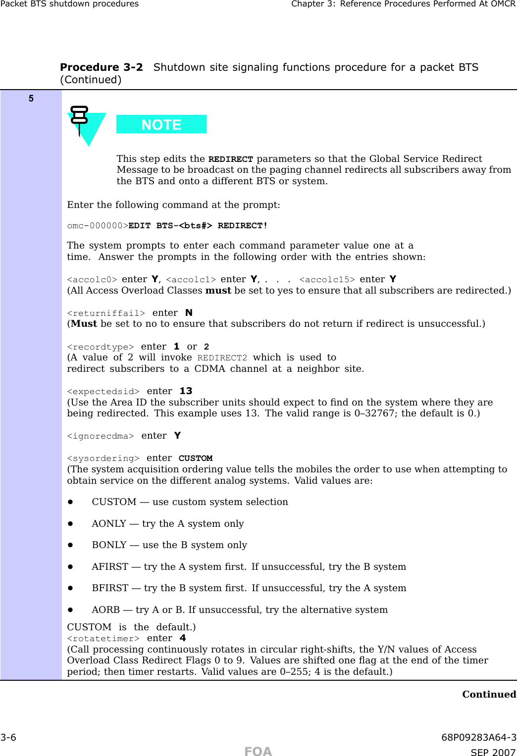
![1X UBS Macro B T S FRU P ack et B T S start -up proceduresProcedure 3 -3 R estore site signaling oper ations procedure for a pack et B T S(Continued)8This step edits the value of the Global Service Redirection Flag ( GLOBALREDIRECT )in the congestion control parameters so that the Global Service Redirect Messageis only broadcast on the sector paging channel when there is traffic congestionin the sectorEnter the following command at the prompt using the applicable BTS number:omc-000000> EDIT BTS-<bts#> CONGESTCONF !9The system prompts to enter each control parameter value one at a time. Skip through theprompts until reaching the following, and enter the parameter shown:<globalredirect> DISABLE(This will revert the Global Service Redirect Message to congestion control.)10When the system displays the values of the control parameters and the following prompt,verify that only the GLOBALREDIRECT value changed.omc-000000>Accept [yes/no]?11If only the GLOBALREDIRECT value changed, enter Yto accept the change.(Now the Global Service Redirection Message will only be sent over the sector pagingchannels when there is traffic congestion in the sector .)12V erify that the CONGESTCONF globalredirect is disabled for each carrier at the BTS byentering the following command at the prompt:omc-000000> DISPLAY BTS-<bts#> CONGESTCONF13Display the status of the signaling REDIRECT parameters for all carriers equipped for theapplicable BTS by entering the following command at the prompt:omc-000000> DISPLAY BTS-<bts#> REDIRECT14Examine the values in the system display response to be sure they match the values input instep 5 of Procedure 3-2 .Continued68P09283A64 -3 3 -11FOA SEP 2007](https://usermanual.wiki/Nokia-Solutions-and-Networks/T5JX1.Exhibit-8b/User-Guide-1056989-Page-94.png)
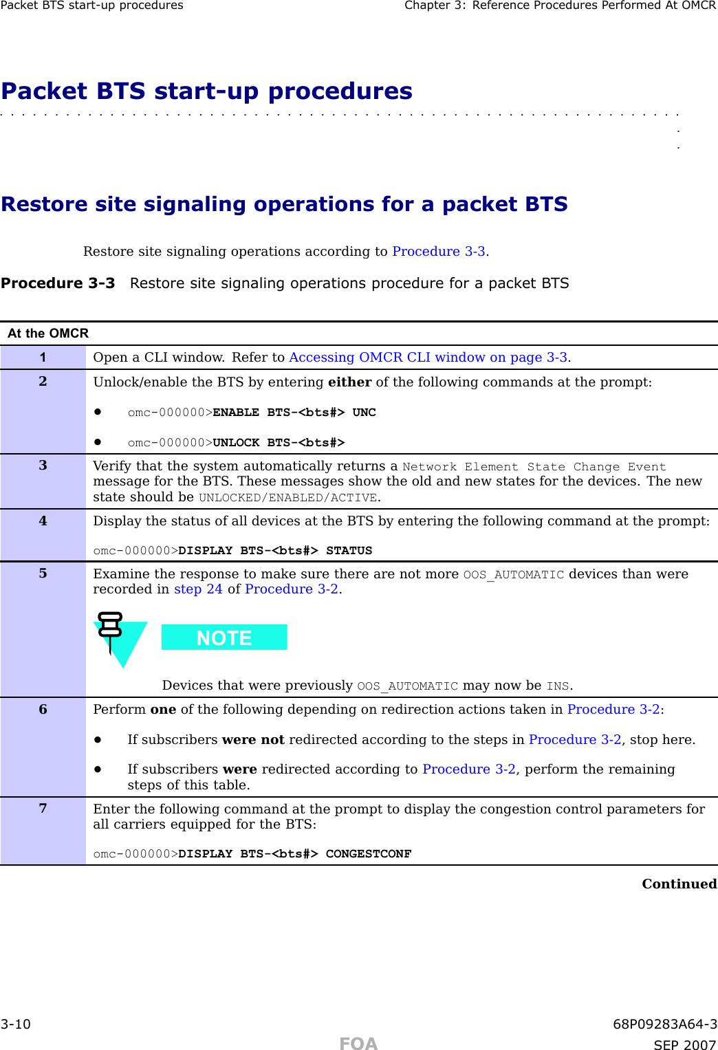
![P ack et B T S start -up procedures Chapter 3: R eference Procedures P erformed A t OMCRProcedure 3 -3 R estore site signaling oper ations procedure for a pack et B T S(Continued)15In this step, use the values recorded in step 4 of Procedure 3-2 to answer theprompts for the EDIT BTS REDIRECT command, except for <recordtype> , enter 2.Restore the values of all REDIRECT parameters by entering the following command at theprompt:omc-000000> EDIT BTS-<bts#> REDIRECT !The system prompts to enter each command parameter one at a time. Answer theprompt in the following order:The following specified values are consistent with the original example. Actualvalues may vary .<accolc0> enter N,<accolc1> enter N, . . . <accolc15> enter N<returniffail> enter N<recordtype> enter 2<expectedsid> enter 0<ignorecdma> enter N<sysordering> enter CUSTOM<rotatetimer> enter 416A fter all parameters are entered, the system displays the command to be sent and the promptbelow . V erify the command syntax is correct.omc-000000>Accept [yes/no]?17A t the prompt shown in step 16 , enter Yto accept the command or Nto go bottom and enterthe correct value(s).18Enter the following command at the prompt to display the status of the signaling REDIRECTparameters:omc-000000> DISPLAY BTS-<bts#> REDIRECT19Ensure that the values in the system display response matches with the values input by theoperator in step 15 .3 -12 68P09283A64 -3FOA SEP 2007](https://usermanual.wiki/Nokia-Solutions-and-Networks/T5JX1.Exhibit-8b/User-Guide-1056989-Page-95.png)