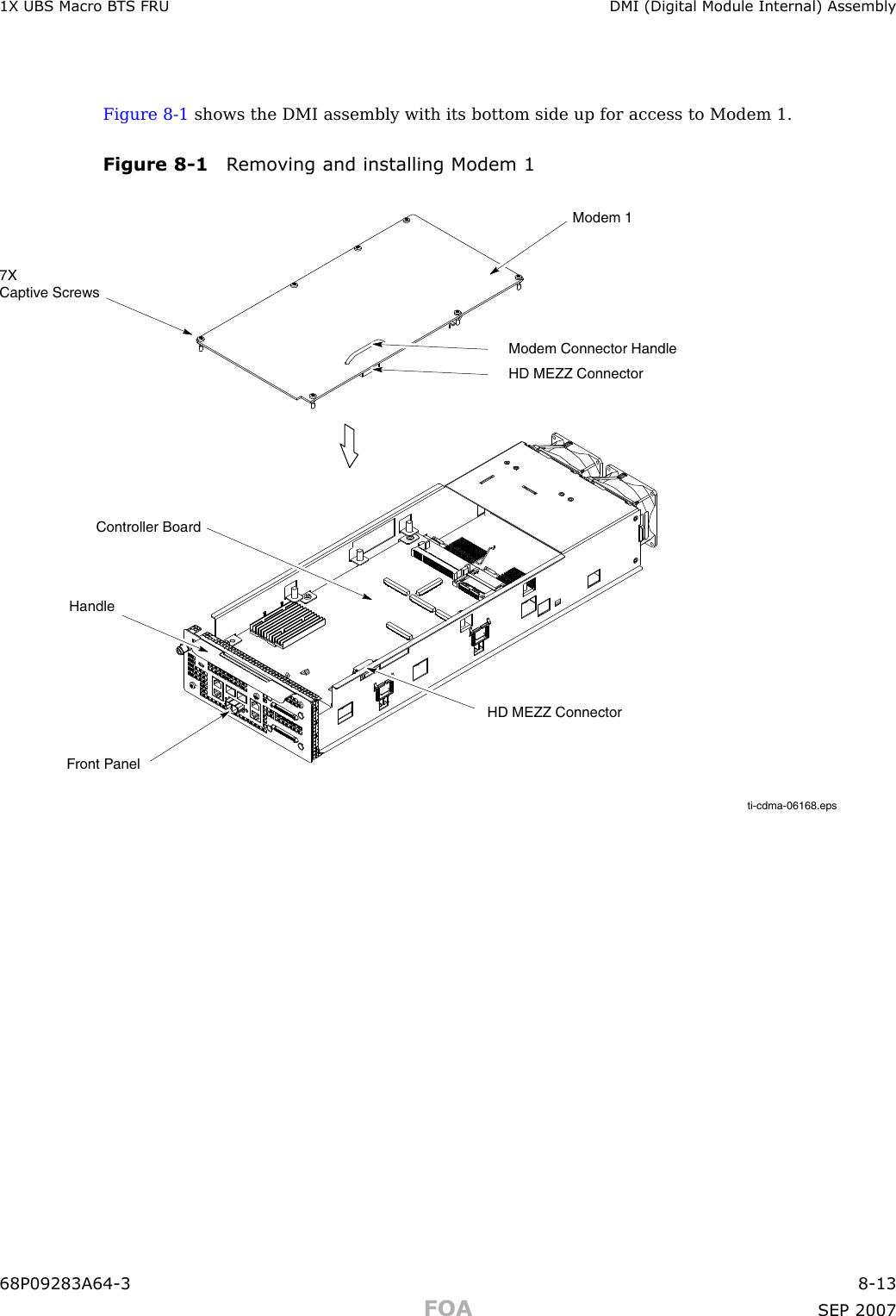
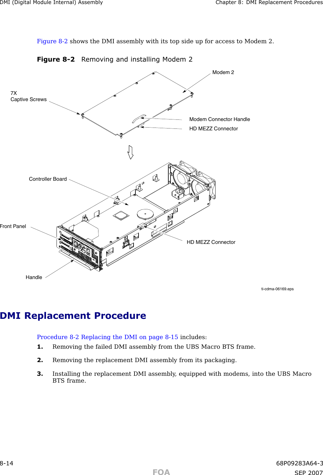
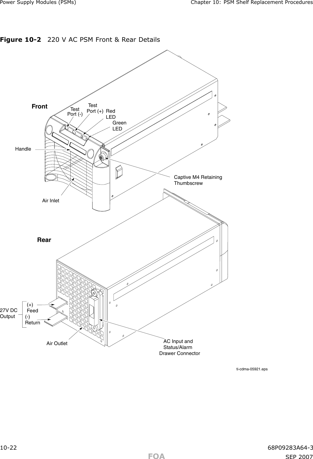
Nokia Solutions and Networks T5JX1 UBS CDMA XMI Transceiver at 800 MHz User Manual Exhibit 8c
Nokia Solutions and Networks UBS CDMA XMI Transceiver at 800 MHz Exhibit 8c
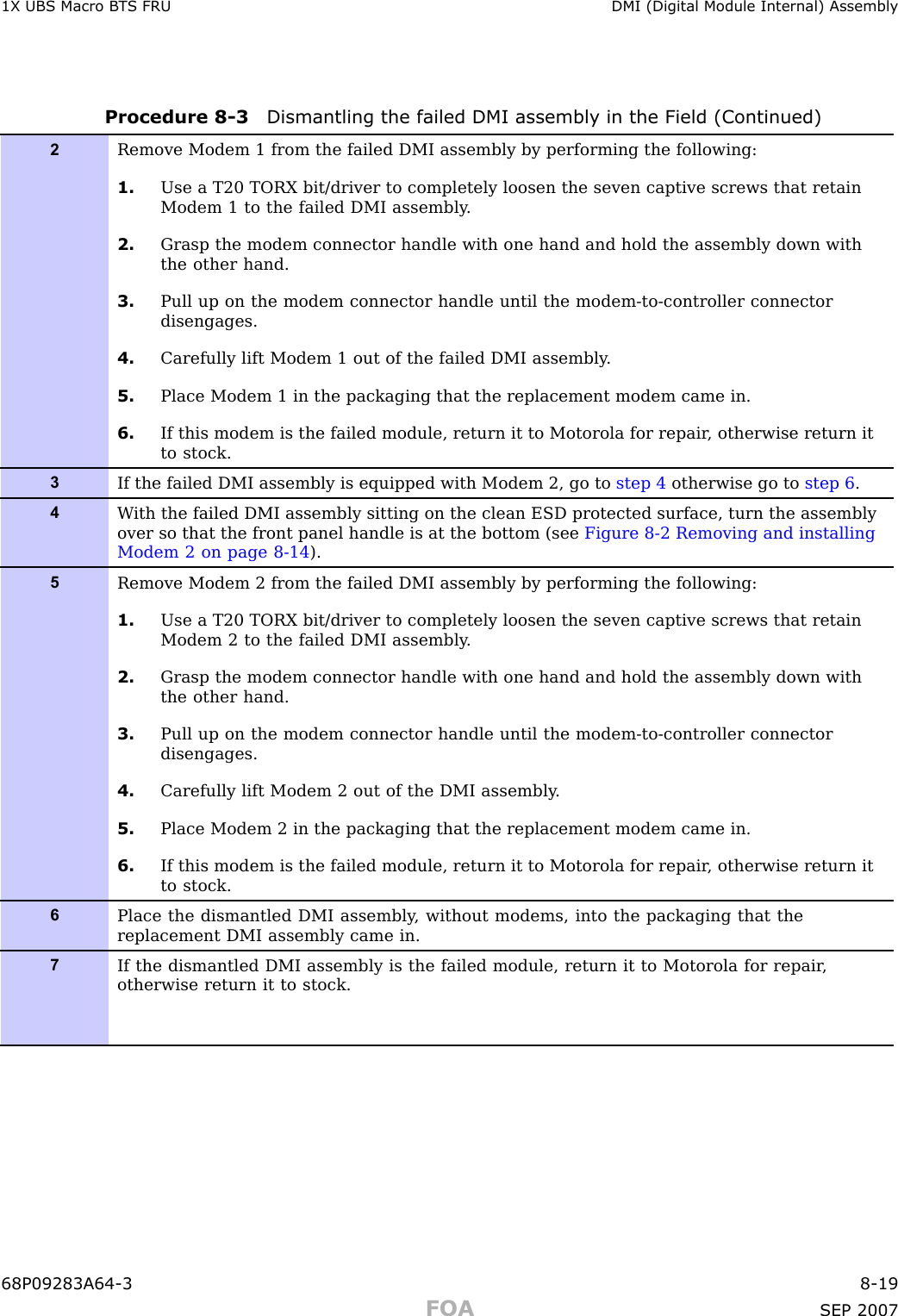
UserManual.wiki
>
Nokia Solutions and Networks
>
T5JX1 User Manual
>
Exhibit 8c
Contents
1.
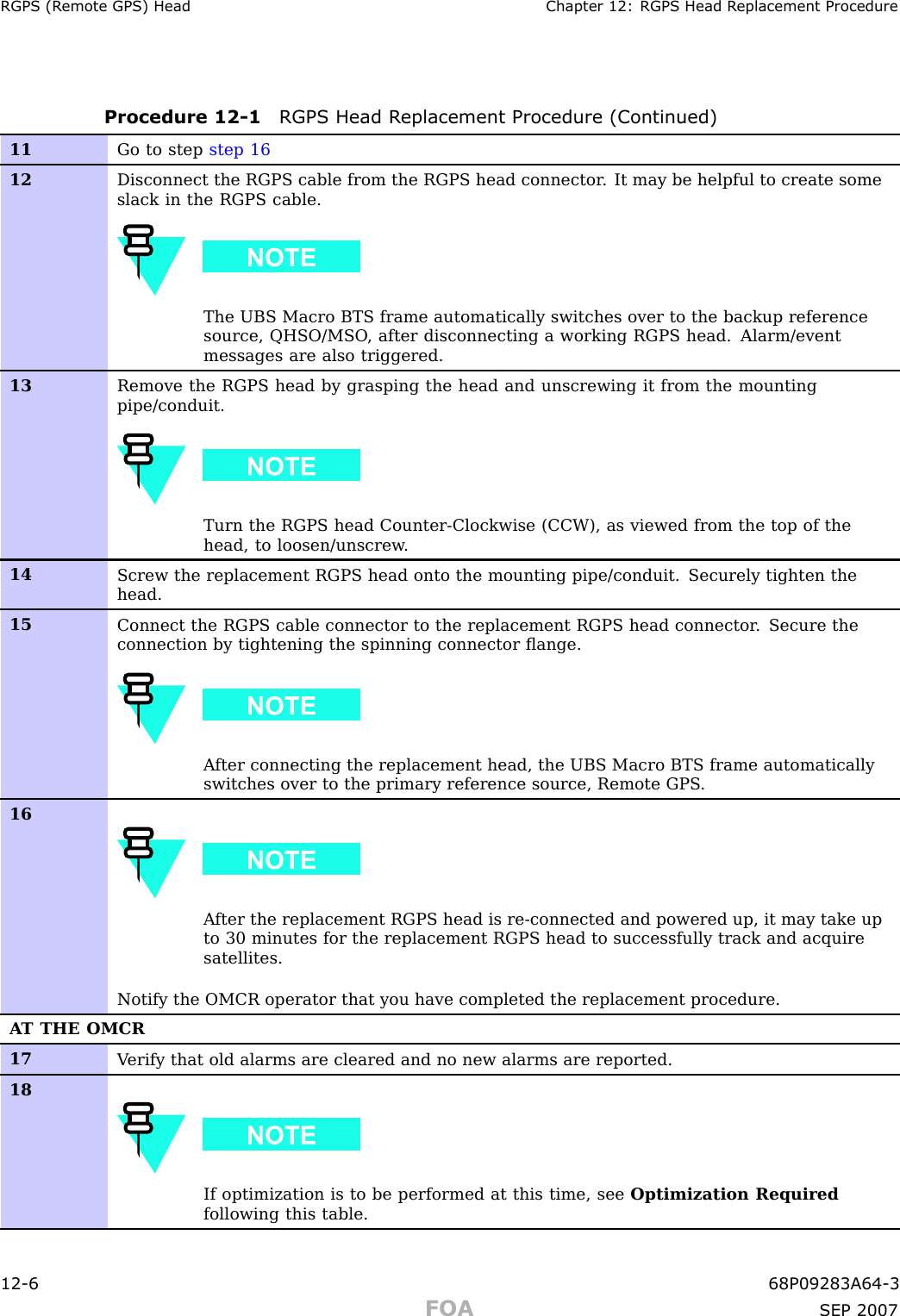
Exhibit 8a
2.
Exhibit 8b
3.
Exhibit 8c
4.
Exhibit 8d
5.
Exhibit 8e
6.
Exhibit 8f
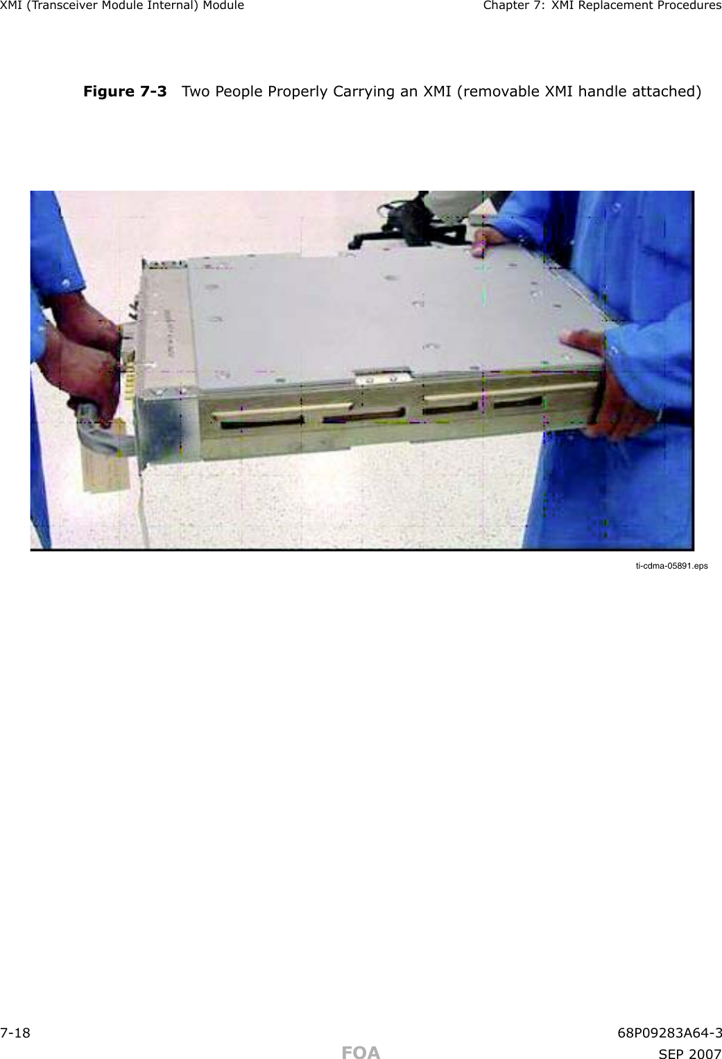
Exhibit 8c
Navigation menu
Upload a User Manual
Namespaces
Wiki Guide
HTML
PDF
Info
Views
User Manual
Discussion / Help
Navigation