Thomson Broadcast and Multimedia LBD-25200 Affinity L-Band Transmitter for Mobile Media Svs. User Manual Affinity LBD 200C N1 DRAFT1
Thomson Broadcast & Multimedia, Inc. Affinity L-Band Transmitter for Mobile Media Svs. Affinity LBD 200C N1 DRAFT1
Contents
- 1. Software Users Guide
- 2. 200W User Manual part 1
- 3. 200W User Manual part 2
- 4. 200W User Manual part 3
200W User Manual part 2
Exciter Configuration Description - 55 -
®
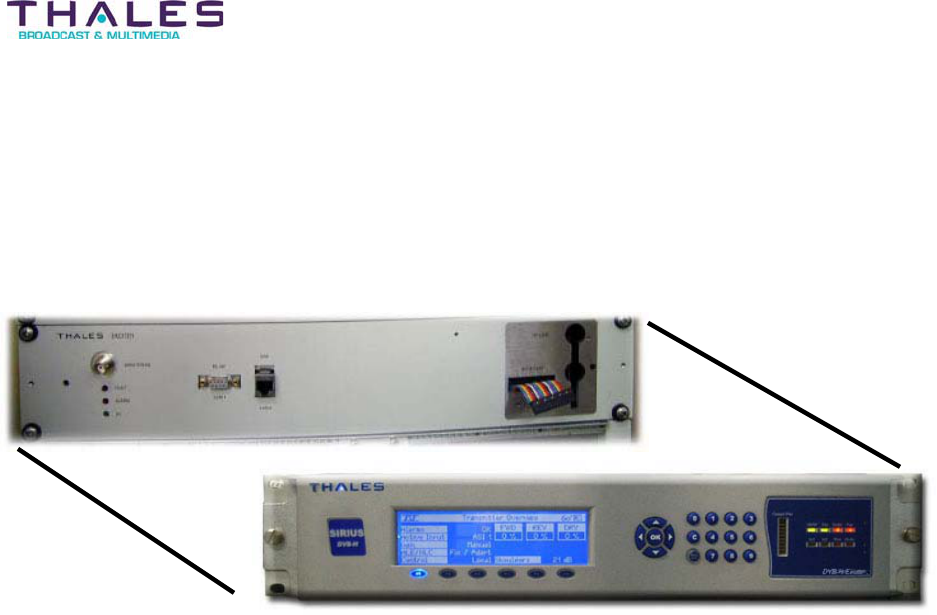
Affinity LBD-200C-N1 Transmitter
Product Manual
10.1.3 General Description
Sirius is a digital TV transmitter Signal Processing Unit sub-assembly that receives an MPEG-2
data stream, and transmits a pre-corrected DVB-H RF signal to the pre-amplifier and power
amplifier. The pre-amplifier is required for high power transmitters.
10.1.4 Main Features
Channel Modulation: The DVB-H channel modulator utilizes a very similar hardware platform
to the ATSC and DRM architectures.
Linear and Non linear pre-correction: by way of an integrated Digital Pre-corrector, a Linear
Equalizer enables correction of the linear distortions caused by the cavities, filters, and antenna
combiner following the HPA power amplifier.
Clipping: allows the reduction of the signal peak-to-average ratio at a programmable value, and
the associated digital filter of the shoulders. This allows a significant reduction of the Back-Off in
the HPA depending on the allowed quality degradation of the signal in terms of END or EVM.
UHF IV/V: A synthesizer generates the output frequency.
Internal air-cooling: Provides adequate cooling to ensure proper operation across specified
temperature range.
Exciter Configuration Description - 56 -
®
Affinity LBD-200C-N1 Transmitter
Product Manual
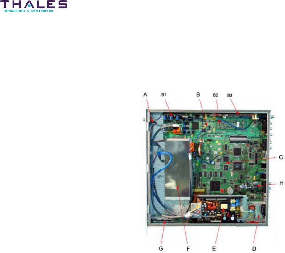
10.1.5 Sirius Subassembly Description
The Sirius DVB-H Exciter is housed in a “19” 2U EIA rack unit and is populated with the
following assemblies:
A- LED board
B- TS board
B1- Enhanced QoS measurement board
B2- IF Filter board
B3- UHF transmitter board
C- Digital board
D- AC Transformer
E- Power Supply
F- Synthesizer
G- PC Slot
H- GPS Receiver
10.1.5.1 Digital Board
Functional Description of Digital Board
The “Digital Board” is built around the combination of an FPGA and a powerful microprocessor.
It supports most of the input/output interfaces and base-band processing from the incoming data
stream up to an I/Q base-band output.
The transport stream input signal is based on the DVB-H Digital Television Standard. The
exciter includes Dual A and B asynchronous serial interface (ASI) inputs in a 75-ohm BNC
female connector, conforming to DVB-ASI (TR 101211). The ASI format is a 188, 214 burst or
byte mode. The equipment adapts automatically to the net input rate since the input rate is
lower than the channel capacity. The dual inputs can be configured as redundant ASI switched
inputs. The DVB-H RF exciter has built in capability to monitor the presence and consistency
(synchronization bytes) of the incoming TS, and produce appropriate alarms. This feature
includes MIP identification (DVB standard), in single frequency network (SFN) as well as multi
frequency network (MFN) modes. This function is performed simultaneously on each different
ASI input.
The equipment is able to manage MFN or SFN operation. The incoming serial data stream
signal is processed by the DVB-H channel encoder, which performs the following functions:
x Removal of the MPEG sync byte

Exciter Configuration Description - 57 -
®
Affinity LBD-200C-N1 Transmitter
Product Manual
x Transport Stream Identification
x Data Randomization
x Reed-Solomon Encoding
x Data Interleaving
x Trellis Coding
x Grey mapping
x FFT
x Pilot Insertion
x Guard interval insertion
The main objective of the Digital Board is to generate an output complex signal in the form of
parallel I and Q digital signals. In addition, the Digital Board provides the clock reference for all
the other boards within the DVB-H exciter. The system is fully compliant with the EN 300-744
1.5.2 Digital Television Standard.
Additional optional functions such as a built in GPS receiver, or DVB receiver, are supported by
additional daughter boards managed by the embedded microprocessor.
This version is designed 3-Mgate FPGA hardware and is dedicated to DVB-H. The incoming
serial data stream signal is processed by the channel encoder, which provides an output
complex digital signal in the form of parallel I and Q digital signals, and a clock reference. The
channel encoder has a hardware version allowing performance of DVB-H modulation. For DVB-
H, all standard modes are supported including hierarchical modes. The equipment can support
redundant switching input for DVB operation. The equipment is also capable of managing either
single frequency networks (SFN) or multi frequency networks (MFN) operation. Bit Rate
Adaptation with PCR re-stamping is used for MFN operation. An embedded microprocessor
manages daughter boards such as a global positioning satellite (GPS) receiver, DVB-H receiver
and TS Board. RS232, I2C and SPI buses are used for internal control and monitoring of the
daughter boards. External control and monitoring is done through RS232 and/or Ethernet and/or
CAN bus. The digital board distributes pilot clocks to Sirius boards, 10MHz to the synthesizer
and TS Board, and system clock to the TS Board.
10.1.5.2 TS Board
Functional Description of TS Board
The “TS Board” is also equipped with an FPGA. It supports the up-conversion and adaptive pre-
correction processing. The TS Board receives the I/Q base-band signal and the clock reference
from the Digital Board. The TS Board performs the following processing:
x Clipping
x Non-Linear Digital Adaptive Precorrection
x Linear Equalization
Exciter Configuration Description - 58 -
®
Affinity LBD-200C-N1 Transmitter
Product Manual
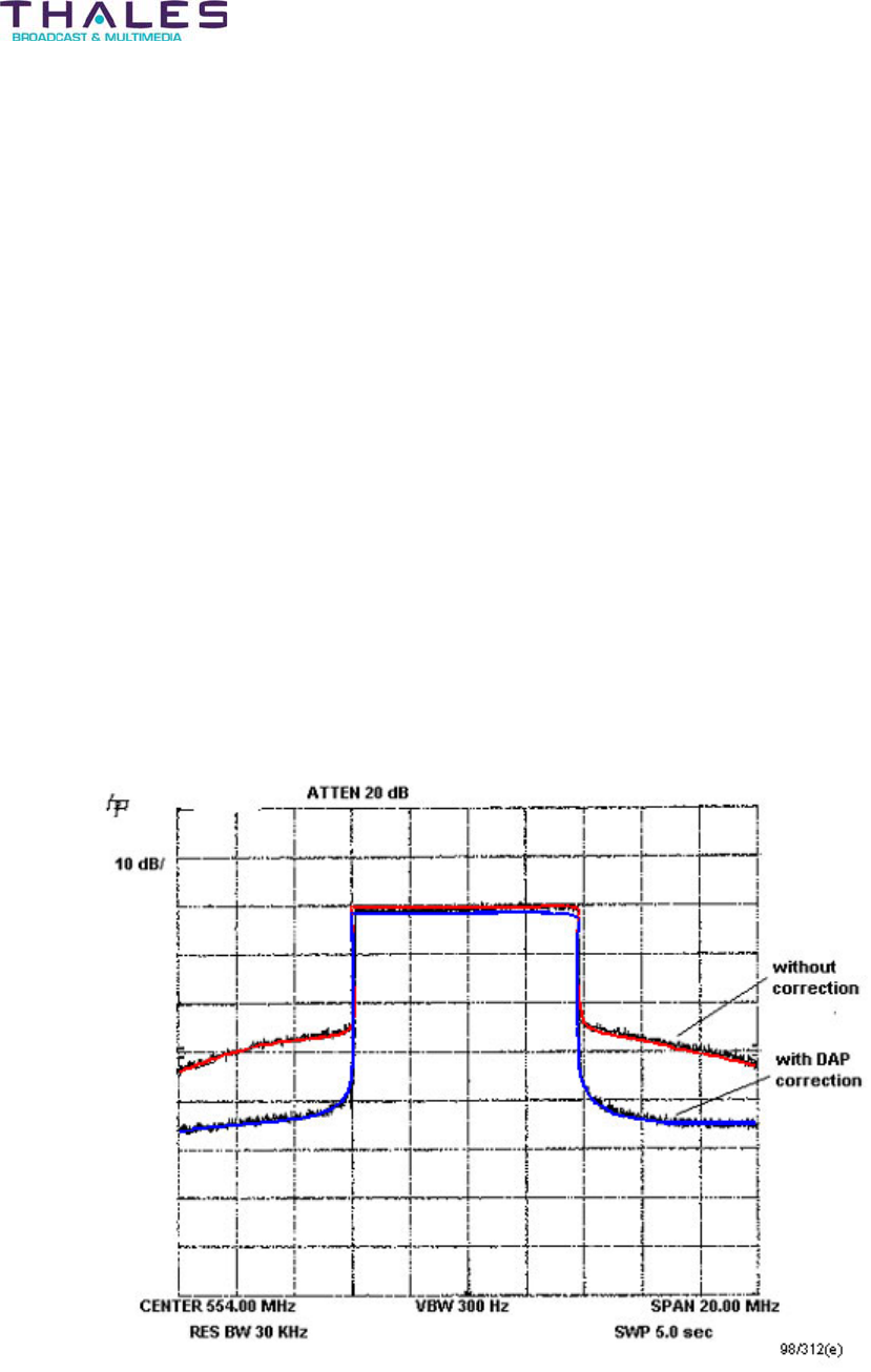
The proprietary clipping function limits the magnitude of the vector above a given threshold. The
magnitudes higher than the threshold are replaced by the threshold complex value. This allows
for a better quality output signal at a lower back-off compared to other transmitters.
The non-linear automatic precorrection function computes the best shoulder level at the output
of the transmitter. The process is based on a Look Up Table (LUT) that is loaded from an
iterative measurement of the shoulder level. The Digital Adaptive Pre-correction (DAPTM) inputs
the I and Q signals from the Digital board and compares them to reference I and Q signals
derived from the output of the transmitter. The DAP™ precisely calculates the correction
needed to make the output signals match the original input signals, and then updates the
forward path in both amplitude and phase to compensate for any differences. The outputs of the
DAPTM board are the fully corrected I and Q signals.
The DAPTM compensates for non-linear distortions, and is able to adapt to drift changes in the
transmitter. Since the correction is adaptive, the set-up and maintenance of the transmitter will
not require a significant investment in time and test equipment, unlike equipment without
adaptive features, the DAP™ signal quality is maintained at all times. Over the lifetime of the
equipment, DAP™ is proven to save operators time and money with lower maintenance costs.
The complex base-band outputs of the LUT are then up-converted to an intermediate frequency
(IF). The complex IF frequency signals are converted to the analog domain, amplified and
transposed to the proper VHF, UHF, or RF band.
A daughter board located on the TS Board performs the Complex Up/Down Conversion (CUDC)
function. The Complex Up/Down Converter (CUDC) receives the pre-corrected signals from the

Exciter Configuration Description - 59 -
®
Affinity LBD-200C-N1 Transmitter
Product Manual
DAPTM and converts them to an analog on-channel RF signal. An internal synthesizer controls
the conversion frequency. The RF local oscillator is always locked by means of a very precise
internal 10 MHz Oven Controlled Crystal Oscillator (OCXO). It can also be locked to an external
10 MHz frequency reference. This synthesizer module also provides the 1000MHz RF local
oscillator for a second upconversion within the transmitter. In this conversion stage, the 670-
675MHz UHF output is translated to the proper on-channel output frequency of 1670-1675MHz
A feedback sample from the RF signal at the output of the transmitter is used to control the
shoulders, the linear correction process, and to monitor the quality of the signal.
The CUDC also receives a gain control command from the return path interface for automatic
gain control (AGC). The modulator has the capability to adjust its output power in manual mode
(when AGC is disabled). The AGC signal is used to adjust the output power of the RF signal
from the exciter and to maintain it within specified limits.
The RF signal output of the transmitter is sampled, down converted back to UHF, using the
same 1000MHz local oscillator, and fed back to the exciter. This RF output sample is fed into
the return path interface contained in the CUDU where it is demodulated. The I and Q reference
signals are derived from a reference demodulator also contained in the return path interface.
They are the base-band I and Q signals of the transmitter output sample. These signals are fed
into the DAP™ processing function in order to correct the transmitter system for linear and non-
linear distortions.
The TS Board receives I & Q output signals and a clock reference from the digital board. These
I & Q signals are processed by the TS Board including: Clipping, Linear Equalization, Non
Linear adaptive pre-correction. The Clipping function limits the magnitude of the vector above a
given threshold. The magnitudes higher than the threshold are replaced by the threshold
complex value. The non-linear automatic pre-correction function computes the best shoulder
level at the output of the transmitter. The process is based on a Look Up Table (LUT) that is
loaded from an iterative measurement of the shoulder level. The complex base-band outputs of
the LUT are up-converted to the IF frequency. The complex IF frequency signals are converted
in the analog domain, filtered, amplified and transposed to the UHF Tx Board. A daughter board
installed on the TS Board performs the up conversion function. External feedback from the RF
signal at the output of the transmitter is used to control the shoulder, the linear correction
process, and to monitor the quality of the signal. The TS Board then processes the feedback. A
DVB-H Enhanced QoS measurement board (optional) is plugged into the TS Board. It is a real
time demodulator board used to efficiently monitor the incoming stream. An additional DVB-H
hardware demodulator can be used for quality measurement at the output of the transmitter
(optional).
10.1.5.3 Power Supply
An internal power supply provides +12volts, -12 volts, +5 volts and + 3,3 volts to the exciter
subassemblies.
10.1.5.4 UHF Synthesizer
A digitally programmable synthesizer is provided to deliver a sinusoidal signal at the transmitting
frequency of between 430 and 900 MHz, with an output level of 10 dBm / 50 ohms. This module
Exciter Configuration Description - 60 -
®
Affinity LBD-200C-N1 Transmitter
Product Manual
also provides a second fixed LO frequency of 1GHz; this is used to upconvert the UHF channel
frequency in double conversion microwave applications.
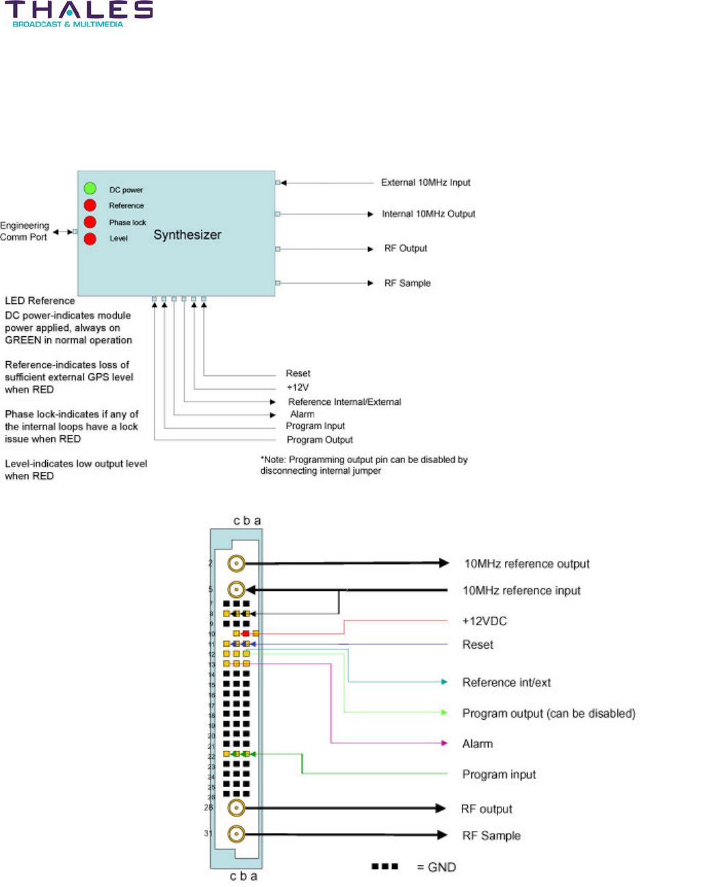
Synthesizer I/O diagram
External synthesizer interfaces

Exciter Configuration Description - 61 -
®
Affinity LBD-200C-N1 Transmitter
Product Manual
The synthesizer sub-module design combines Direct Digital Synthesizer (DDS), and Phase
Lock Loop (PLL) technology to allow for wideband, low resolution, and low phase noise
performance. Combining a DDS with a PLL in an RF synthesizer allows frequency resolution
and controllability of the DDS while maintaining the frequency range of the PLL system. The
PLL can reduce DDS spurious, whereas the DDS can decrease PLL multiplication factor,
enhancing phase noise performance of the overall system. Together they provide for a high
performance RF synthesizer. This design is a modified translation loop approach containing
three phase locked loops, however its core operation depends on a single main loop with an
embedded direct digital synthesizer, allowing a simpler overall architecture as compared to
traditional multi loop synthesizers, a design method previously hard to achieve without the use
of a custom ASIC or complex multistage architecture. The highly integrated direct digital
synthesizer incorporates many of the design stages necessary for the translation loop approach
such as integrated PLL and mixer stages. Proprietary circuits and techniques allowing wideband
operation with fine step size resolution are applied.
To maintain frequency stability the synthesizer requires a reference frequency. Two options are
offered in this design, a 10MHz external reference and/or an internal reference. In the internal
reference, a PLL system locks an on-board voltage controlled Oven Controlled Crystal Oscillator
(OCXO) to the incoming reference input allowing the external reference to control the internal
reference while present, and allows minimal system impact in the event that the external
reference is lost. The internal reference oscillator circuitry will sense the presence of the
external source and select this source as the primary frequency stability determining input. In
the event that the external reference is absent, the synthesizer will automatically substitute a
voltage on the OCXO V-tune input. This methodology is more complex and costly but adds
reliability to SFN transmission systems by allowing a phase continuous input to the synthesizer.
Usually, the external reference frequency is a signal that is obtained from a GPS or Loran C
broadcast. These navigational broadcasts frequencies are driven from a master reference
oscillator that is traceable to a NIST level-1 frequency clock. The external reference enters the
module through an RF female coaxial contact of the DIN41612-M connector. The input is
matched using a resistive load for 50-ohm impedance. An output of the PLL processed internal
reference is also offered on a separate RF female coaxial contact of the DIN41612-M
connector. The incoming signal is sampled and detected by a logarithmic amplifier detector.
This information, in the form of an analog DC voltage proportional to the signal level, is sent to
the MCU for diagnostics. An LED present on the front panel indicates reference status. The
reference signal is limited so that the level at the input connector can be as high as +30dBm
with no damage to the input circuitry, however, a nominal level of +5dBm is recommended and
a level above -5dBm should always be maintained. Note that the phase noise of the reference
will affect phase noise performance of the LO outputs. The main Phase Lock Loop (PLL) uses a
wide loop bandwidth, and reference noise is one of the dominating factors determining phase
noise at close offsets to the carrier below the loop filter cutoff. The client should exercise caution
when selecting the reference source if the internal OCXO option is not installed. In order to
minimize cost impacts, the high stability internal OCXO reference will remain an option that the
client must request at time of order. The 10MHz signal also forms the reference input to the
1000MHz PLO.

Exciter Configuration Description - 62 -
®
Affinity LBD-200C-N1 Transmitter
Product Manual
The Synthesizer Menu System:
The synthesizer is equipped with a menu system that can be accessed via the RS232 port
located on the front panel. Any terminal application can be used. A serial interface cable
(consult cable drawing 47267081-040 for construction details) is connected from the front panel
RS-232 RJ11 connector to an available serial communication port on a PC (set to 9600baud).
Open the terminal application and ensure proper communication settings. To display the current
module status type “:?” followed by a carriage return. The current status and list of available
commands will appear; the following example illustrates the display activity:
Thales B&M.
:?
***************************************************************
Synthesizer Status
***************************************************************
Current frequency setting: 700000000Hz
On-board OCXO: Yes
Reference INT/EXT: Internal
Reference Level: Optimal
Reference ATD value: 72 (threshold=119)
Free running OCXO control value: 691
10MHz PLL Health: Locked
1000MHz PLL Health: Locked
Main PLL Health: Unlocked
Current loop filter switch: Engaged
RF output ATD value: 72 (threshold=160)
Mute switch state: Muted
Current attenuator value: 255 (default=255)
Alarm status: Alarm (state = 8)
******************** Synthesizer Commands *********************
:? Show Status :V Show Version :L Test LEDs
:a Show Attenuation :A<atten> Set Attenuation :X Set OCXO
:R Reset Synthesizer :E<freq> Set Frequency :F Toggle LFC
:0 Show A2D 0 :1 Show A2D 1 :2 Show A2D 2

Exciter Configuration Description - 63 -
®
Affinity LBD-200C-N1 Transmitter
Product Manual
NOTE: Use the commands in the same way you invoke the status screen; type “:” then the
appropriate letter for the desired command followed by a carriage return.
Command functions (front port only):
:? Show Status
To get current module status, type “:”; then “?”; then press enter.
This command will display the current status of the module
:V Show Version
To get module version info, type “:”; then capital “V”; then press enter.
This command will display the Module part number, firmware revision, build date, and other
version information.
:L Test LEDs
To check LED status and run lamp test, type “:”;L then press enter.
This command invokes a lamp test routine.
:a Show Attenuation
To check current attenuator value, type “:”; small “a”, then press enter.
This command displays the current attenuator setting.
:A<atten> Set Attenuation
To set the attenuator, type “:”; capital “A” then 3-digit attenuator setting 0-255 then press enter.
This command allows adjustment of the output level. The valid setting range is 0-255, 0 having
the maximum RF level and 255 having the lowest. The typical value will be around 190 to
achieve the proper nominal level. The RF output can be adjusted to work with a +17dBm mixer
as well as today’s 12dBm output level.
:X Set OCXO
To set the free-running OCXO frequency, type “:”; capital “X” then the setting.
This command allows adjustment of the free running OCXO. Meaning if the external reference
is not present and the module is equipped with the internal oscillator the tuning port voltage can
be adjusted to compensate the frequency of the internal oscillator. This acts as the hardware
potentiometer adjustment used in OEM models. The typical value will be between 690 and 850
to achieve the proper RF frequency.

Exciter Configuration Description - 64 -
®
Affinity LBD-200C-N1 Transmitter
Product Manual
:R Reset Synthesizer
To reset the module, type “:”; capital “R” then press enter.
This performs a software reset, be aware that invoking reset will force a temporary mute of the
output.
:E<freq> Set Frequency
To set frequency, type “:”; capital E then 10 digit frequency ex: 0500000000; then press enter
Use this command to change the frequency of operation. Always enter a full 10-digit frequency
after the command character.
:F Toggle LFC
To set LFC: type, “:”; capital “F”; then hit enter. (Toggles current value engages or disengages
the circuit)
This allows the user control over the loop filter bandwidth, and can be used to override the
default setting. The user should use caution, and be monitoring the phase noise characteristics
of the output during this adjustment.
:0 Show A2D 0
To check reference detector ATD value, type “:”;0 then press enter.
This displays the external reference level after the analog to digital conversion.
:1 Show A2D 1
To check RF level ATD value, type “:”;1 then press enter
This displays the output level after the analog to digital conversion.
:2 Show A2D 2
Unused at this time
Command functions (REAR port only):
Exciter Configuration Description - 65 -
®
Affinity LBD-200C-N1 Transmitter
Product Manual
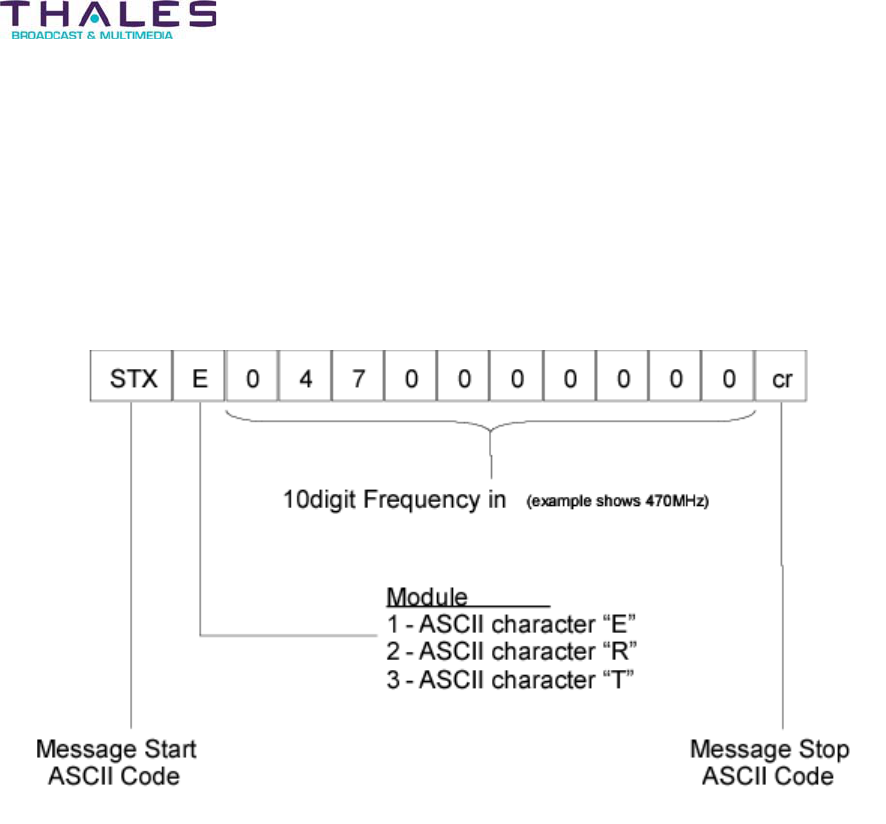
The rear panel RS232 communication port operates at 1200baud, and can be interfaced via any
terminal application. This port is limited to changing the output frequency. Selection of the
output frequency is made by using a proprietary protocol that sends a 10 digit ASCII character
string across the rear panel serial bus at a transfer rate of 1200baud, No parity, 1 stop bit. The
synthesizer firmware will not accept alpha or symbolic characters as part of the frequency data.
The Figure below demonstrates the messaging sequence:
To manually set a new frequency: type cntrl b; capital “E”; then type the10-digit frequency (ex:
0500000000), and press enter.

Exciter Configuration Description - 66 -
®
Affinity LBD-200C-N1 Transmitter
Product Manual
DC Power Requirements / Synthesizer Specifications
The module requires a single 12VDC source entering on pin B10 of the 60-pin DIN connector.
Parameter Specification Comments / Notes
Voltages / Currents +12 VDC r.5 @ 850mA max.
+12 VDC r.5 @ 1.5A max.
w/o internal reference
w/ internal reference
Ripple <1mV Pk-Pk Allowable on external source
Connector DIN41612 type M connector. 60
conductor, 2amp / circuit; performance
level 1
Interfaces to back-plane
Reference Specifications (applies to external reference except where indicated)
Parameter Specification Comments / Notes
Frequency 10MHz External or optional internal
Input Level 0 dBm +15 /-5dB (+48 dBmV nominal) +30dBm no damage
Format Sinusoidal
Stability vs. temp.
External MRO
Internal OCXO
1x10⁻⁷ PPM minimum 0q-50qC
r2x10-8 PPB minimum 0q-50qCAfter 60 minute warm up; Refer
to Temex
specification/datasheet for long
term ageing specifications
(valid for free-running mode
only)
Non-Harmonic
Spurious
10Hz < ƒoffset < 5MHz < -104dBc
beyond 5MHz < 75dBc
Connector /
Impedance
DIN connector coaxial contact / 50 :For external input and internal
output; Mates with back-plane
connector

Exciter Configuration Description - 67 -
Affinity® LBD-200C-N1 Transmitter
Product Manual
RF output specifications
UHF Band430-900MHz
Parameters Specifications Comments / Notes
Frequency Tuning
Range
430-900MHz Covers UHF Band
Tuning Step Size
Coarse
Fine
N/A
1Hz
Non-Harmonic Spurious 100Hz < ƒoffset < 10MHz, 65dBc
beyond 10MHz < 65dBc
SSB Phase Noise
(typical)
See UHF mask for
guaranteed limits
d65 dBc/Hz @ 10Hz offset
d85 dBc/Hz @ 100Hz offset
d90 dBc/Hz @ 1kHz offset
d104 dBc/Hz @ 10kHz offset
d115 dBc/Hz @ 100kHz offset
d130 dBc/Hz @ 1MHz offset
Depends on frequency reference
source. The reference must be
d140 dBc/Hz @ 100Hz offset;
Measured with Thales standard
OCXO based MRO. Phase noise
specifications below loop
bandwidth based on system noise
floor = –213+10log ƒcomp + 20log
N.
VHF Band 54-300MHz
Parameters Specifications Comments / Notes
Frequency Tuning
Range
54-300MHz Covers VHF Bands I,II,&III
Tuning Step Size
Coarse
Fine
N/A
1Hz
Non-Harmonic Spurious 100Hz < ƒoffset < 10KHz, 65dBc
10KHz < ƒoffset < 10MHz, 60dBc
beyond 10MHz < 60dBc
SSB Phase Noise
(typical)
d65 dBc/Hz @ 10Hz offset
d85 dBc/Hz @ 100Hz offset
d101 dBc/Hz @ 1kHz offset
d107 dBc/Hz @ 10kHz offset
d120 dBc/Hz @ 100kHz offset
d135 dBc/Hz @ 1MHz offset
Depends on frequency reference
source. The reference must be
d140 dBc/Hz @ 100Hz offset.
Measured with Thales standard
OCXO based MRO.
Exciter Configuration Description - 68 -
Affinity® LBD-200C-N1 Transmitter
Product Manual
General
Parameters Specifications Comments / Notes
Power Level
Main output
Sample output
+12dBm, r2dB
-7dBm, r3dB
No ALC
Power Level (muted)
Main output
Sample output
<-25dBm
<-43dBm
Time to mute <2ms Hardware controlled
Frequency settling time
After switch on
After last character is
received in a channel
change event
<1s
<700ms
Stability Based on frequency reference; 10-9 to
Allan variance
Harmonics 10dBc minimum
Connector / Impedance
Main output
Sample
DIN connector female coaxial contact / 50
:
DIN connector female coaxial contact / 50
:
Mates with backplane
I/O VSWR 2:1 Ratio
The UHF phase noise mask is shown in the following figure:
10 -65 -80
100 -85 -94
1000 -90 -101
10000 -95 -104
100000 -115 -120
1000000 -135 -140
UHF Synthesizer phase noise mask
-160
-140
-120
-100
-80
-60
-40
-20
0
1 10 100 1000 10000 100000 1000000
SSB Freq Offset (Hz)
SSB noise (dBc/Hz)
Mas k
Typic al
UHF phase noise mask

Exciter Configuration Description - 69 -
Affinity® LBD-200C-N1 Transmitter
Product Manual
Alarms / Indicators / Adjustments / Controls
Alarms/ Indicators/Adjustments/Controls
Parameters Specifications Comments / Notes
DC PWR Presence
Indicator
Green LED, ON= +12VDC power present;
trips when + 12 VDC signal is absent
Visible via front panel
Frequency reference
Indicator
Red LED, ON = External Frequency
reference fault; trips when signal < -
5dBm; normally unlit
Visible via front panel
Level Indicator Red LED, ON= output muted or at low
power; trips when signal <+6dBm;
normally unlit
Visible via front panel
Phase () Lock Indicator Red LED, ON= Loss of Lock or loss of
frequency programming data; normally
unlit
Visible via front panel
Frequency Control Serial interface; Selection of the output
frequency is made by serial programming
using ANACAD proprietary protocol,
which sends ASCII character string
across serial bus operating at 1200buad;
no parity.
Accessible via rear panel serial
connections on 60pin DIN; It will
also be possible to read back the
frequency setting of the
synthesizer.
Frequency Reference
adjustment
(internal reference option
only)
Firmware controlled user adjustment of
internal OCXO reference oscillator for
frequency alignment
Accessible via RJ11 front panel
port use external computer with
LO calibrator application
Front panel
communication/ Control
port
RS-232 interface; used for firmware
upload, setup, calibration, control, and
diagnostics purposes.
Accessible via RJ11 front panel
port use external computer with
LO calibrator application
Reset Control signal input to module; pull-up to
+5V = reset condition
Signal available at rear-panel of
module
Reference int/ext TTL Low = internal ref; HIGH=external ref Signal available at rear-panel of
module
LO Fault TTL Low = fault condition; HIGH=Normal Signal available at rear-panel of
module

Exciter Configuration Description - 70 -
Affinity® LBD-200C-N1 Transmitter
Product Manual
Environmental
Environmental
Parameters Specifications Comments / Notes
Operating Temperature -10qC to 50qCFrequency stability and
functionality guaranteed
Storage Temperature -20qC to 70qC
Specified Temperature
Range
0q to +50qCAll specified parameters
guaranteed
Cooling Natural convection
Relative Humidity 0 to 95% non-condensing
NOTE: Under normal operation Sirius handles all interfacing with the onboard synthesizer therefore
manual interface is rarely utilized and is explained here as reference only.
10.1.5.5 GPS Receiver
The optional low power miniature GPS board enables the onboard 1 PPS signal 10 µs pulse,
UTC, and 10 MHz signals. Refer to The GPS manual for details on this optional device.
Exciter Configuration Description - 71 -
®
Affinity LBD-200C-N1 Transmitter
Product Manual
10.1.6 Exciter Rack
The frame of the exciter includes two complementary devices:
Exciter Front Panel Assemblyx
x PC Card Slot Assembly (optional) used to house a memory board capable of saving
exciter parameters.
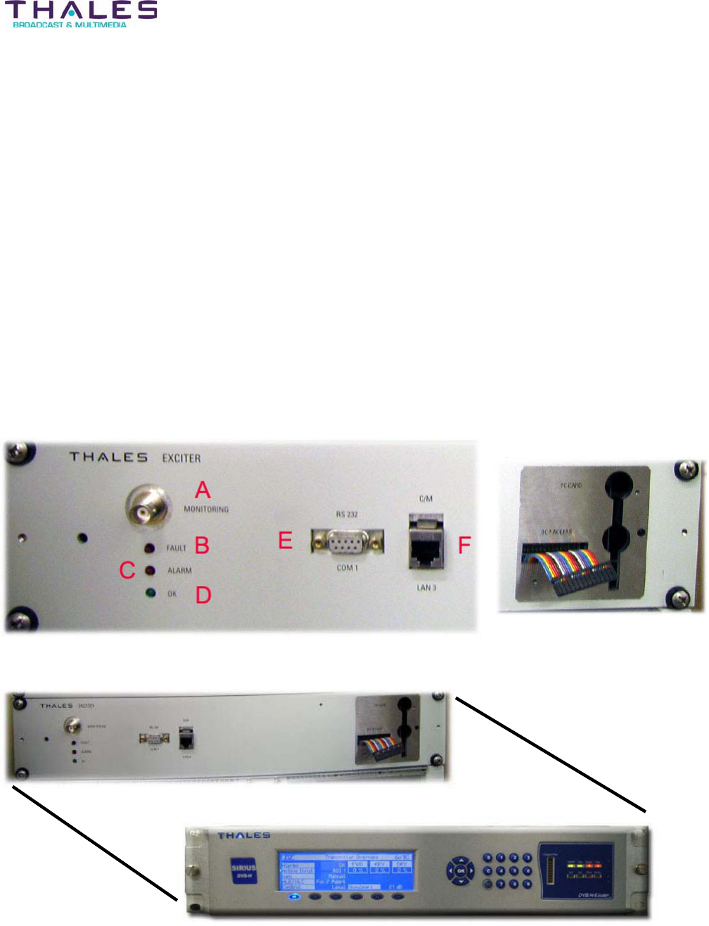
Front Panel Designators
A-Monitoring- Output sample to monitor the RF signal output
B-Fault (LED)- Global detection---checks for faulty boards
C-Alarm (LED)- Checks input data stream and GPS operation
D-OK (LED)- LED has two functions: (1) Power supply presence voltage (2) Start-up of exciter
E-Com1 RS232- RS232 input for programming the Digital Board.
F-LAN- Ethernet access for programming the Digital Board
PC Card Slot (optional)
Exciter Configuration Description - 72 -
®
Affinity LBD-200C-N1 Transmitter
Product Manual
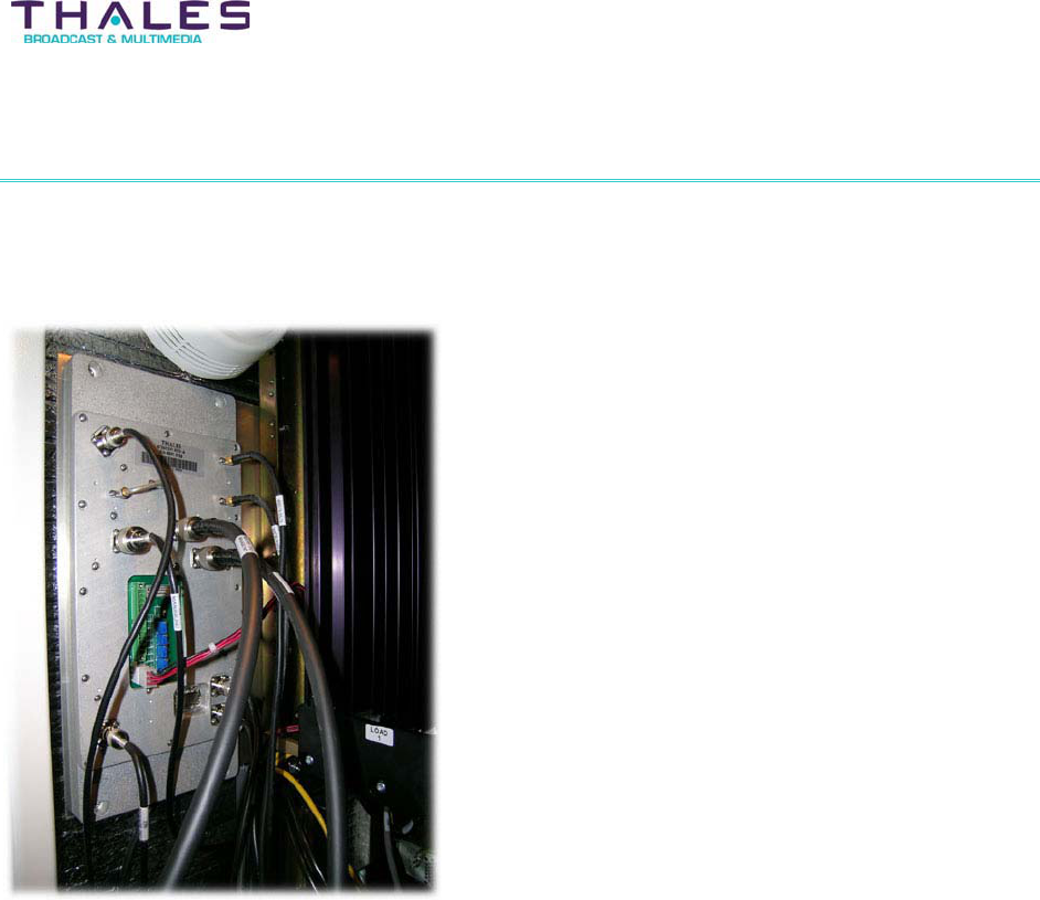
10.1.7 Exciter Connectivity
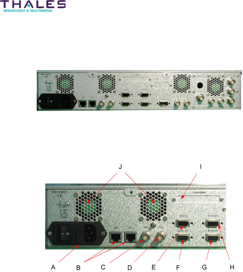
Located at the backside of the exciter are the interconnection points used by the operator to
control the driver function in the transmitter.
Left side of Rack
A- Main power supply input: 90 to 254 volts AC, 47 to 53 hertz
B- 2 RJ45 connections for Ethernet
C- 10 MHz 50 ohm frequency reference input connected to Digital Board
D- Timing reference 1 PPS connected to Digital Board
E- Double input and double output opto-coupled ports in connection with Digital Board
F- DB9 RS232 UTC reference input for GPS
G- DB9 RS232 Local CM in connection with Digital Board.
H- DB9 RS232 data for Digital Board.
I- Multipoint connection I/O extension, monitoring and control interface via contact closure
(optional)
J- Cooling
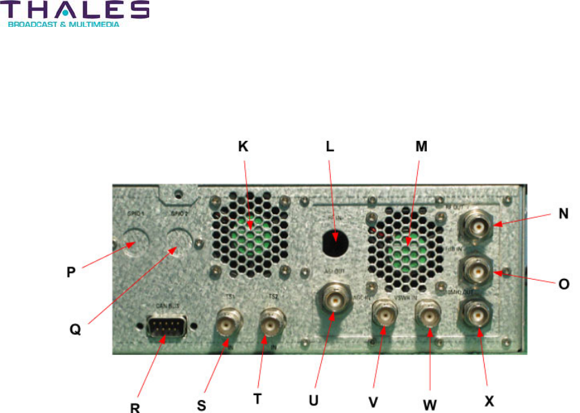
Exciter Configuration Description - 73 -
®
Affinity LBD-200C-N1 Transmitter
Product Manual
Right side of Rack
K- Cooling
L- Synthesizer 1GHz LO output
M- Cooling
N- 0 dBm with 45dB shoulder RF output (without precorrection)
O- Feedback RF input (-15dBm+/-5dB) for linear and no linear automatic correction.
P- GPIO connection (not used)
Q- GPIO connection (not used)
R- CAN bus in connection with Digital Board (not used)
S- DVB-ASI input TS #1
T- DVB ASI input TS #2
U- Optional ASI output
V- Automatic gain control input (not used)
W- VSWR input in connection to TS Board (not used)
X- 10 MHz output signal (not used)

Exciter Configuration Description - 74 -
®
Affinity LBD-200C-N1 Transmitter
Product Manual
10.1.8 General Characteristics of Exciter
Transmission Characteristics
Emission Standard: DVB-H
Norm: ETS 300-744 v1.3.1 or the last
at the date of this specification
Modulation scheme: COFDM
Signal Bandwidth: 5,6, 7, 8, MHz
UHF IV & V 470 @ 862 MHz
Environmental Conditions and Safety
Performance: 0° to 45° C up to 3000 m -10° C to + 50°C
with derating: Tmax - 5°C by 1000 m Maximum altitude: 4000 m max
Storage temperature: -30° C to +60° C Relative Humidity: d 95% sans
condensation
EMC: Standard ETS 300-385 Safety: IEC 215, IEC 1010
CE Label: Compliant Acoustic noise: IEC 179: < 65dBa
General Electrical Mechanical and Cooling Characteristics
Rack: 19" 2RU, depth < 600mm
Main Consumption: < 200 VA
Cooling: Internal Fan, air input on the front panel
Finish: Thales Standard
Mains Power Supply
Voltage 230 V / 105 V r 15%
Frequency 47 to 63 Hz
Power Factor (at nominal operation) > 0.90
Button ON/OFF on the rear panel
Accessible fuse

Exciter Configuration Description - 75 -
®
Affinity LBD-200C-N1 Transmitter
Product Manual
10.1.9 Input/Output Characteristics
Input Characteristics
TS Input
DVB-H version
Dual A and B ASI inputs
Auto, manual, remote switchable for TS securization OR HP and LP inputs for hierarchical
mode
- Standard MPEG 2 TS
- Format: TM 1449: 8 bits/10 bits encoded
- Max. level 800 m Vpp
- Min. level 200 mVpp
- Baud rate 270 Mbaud r 100ppm
- ASI format 188, 204, 188+16
- Impedance 75 :
- Return loss 15 dB from 5 to 270 MHz
- Connector BNC female
- Maximum length of cable between Network adapter and TX input: < 50m
Dual ASI for Hierarchical mode (optional)
- 4 BNC connectors for 2 HP and 2 LP ASI inputs
Dual A and B PDH inputs (ETS 300 813)
Dual A and B SDH inputs (ETS 300 814)
Ancillary Inputs
External 10 MHz Frequency Reference
- Standard 10 MHz
- Format: Sinus and TTL
- Level 7 dBm r1 dB
-Return loss 17 dB
- Connector: BNC female
-Impedance 50 :
- Phase noise DVB-H compliant: at 10 Hz d –110 dBc/Hz, at 100 Hz d – 130 dBc/Hz. Spurious
d –104 dBc/Hz from 10Hz to 5 MHz.
External Timing Reference (1 PPS)
- Pulse width min 50 Ps
- Level TTL

Exciter Configuration Description - 76 -
®
Affinity LBD-200C-N1 Transmitter
Product Manual
- Frequency 1pps
- Active Edge choice for leading or falling edge
- Connector BNC female
- Impedance 50 :
Input for non linear correction (feedback)
- Input level: -26 < N < -20 dBm
- Connector BNC female
- Impedance 50 ohms
- Return Loss >15 dB
AGC Input
- Average detected voltage: 1 < N < 2,5V -
- Connector BNC female
- Impedance > 3 K ohms
- Range: 10 dB
- Rise time and fall time < 1s
- Switch over threshold for MGC 200mV
RF Output Characteristics
Standard
- DVB-H 8/7/6/5 MHz Capability to follow possible modifications of the standards
Power
- Output power (rms) 0 dBm
- Adjustable between +0 and –10 dB by 0.1 dB steps
- Output power stability r 0.2 dB
Output connector
- Impedance 50 :
- Connector BNC
- Return loss t 20 dB
Frequency
- Frequency range (RF Output) frequency agile, without tuning, from 470 to 862 MHz
- Step 1 Hz
- Intrinsic Frequency stability < 1.10-7/year

Exciter Configuration Description - 77 -
®
Affinity LBD-200C-N1 Transmitter
Product Manual
- Phase noise compliant with Validate mask
Intrinsic In Band Output signal quality
Modulation shall be generated digitally
- Global MER (DVB-H) t 36 dB
- MER per carrier (DVB-H): t 33 dB
- EVM on each carrier: < 1%
- Central carrier rejection 60 dB under the DVB-H power or t30 dB under the central pilot
amplitude
- BER before Viterbi (DVB-H) d 1 10-6
- END d 0.1 dB
- In Band spectrum flatness dr 0.2 dB
- Group delay ripple dr 10ns
Driver Section - 78 -
®
Affinity LBD-200C-N1 Transmitter
Product Manual
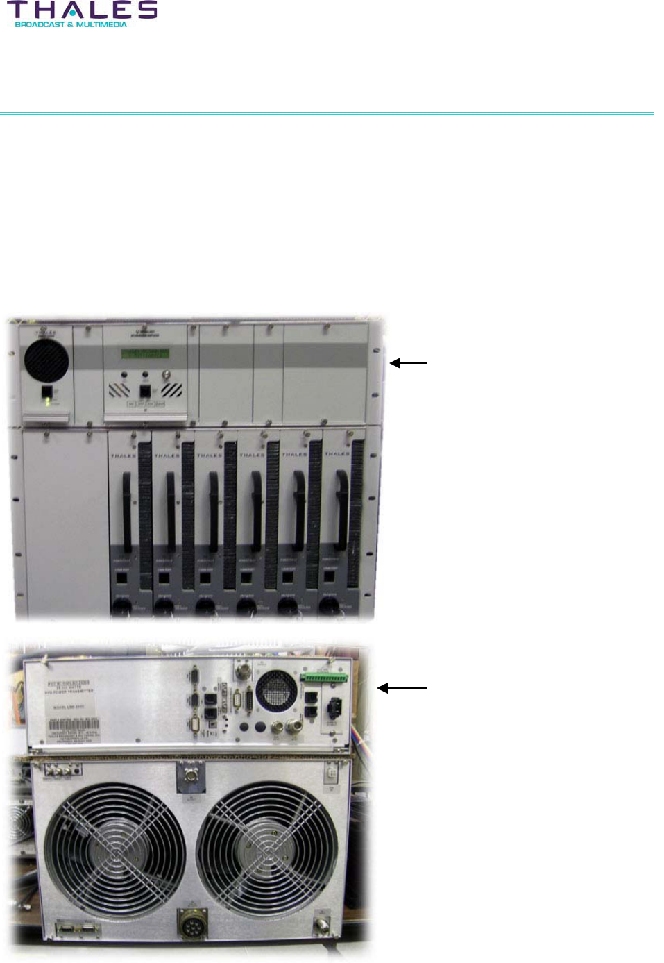
11 Driver Section Description
The Driver Section up-converts and pre-amplifies the IF input signal from the modulator to the
levels required to excite subsequent stages. The Power Supply Plug-in Module and the
Upconverter Module sub-assemblies make up the Driver Section. These sub-assembly modules
are accessible through detachable covers. The covers, which direct airflow through the Driver,
together with the rear panel fan-assembly, are part of the Driver Section forced-air convection
cooling system.
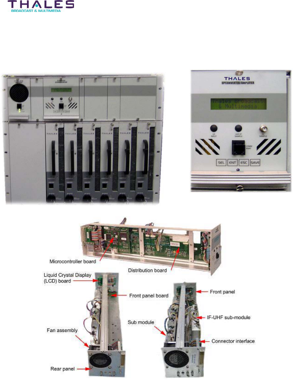
Driver Assembly (Front view)
Driver Assembly (Rear view)
Driver Section - 79 -
®
Affinity LBD-200C-N1 Transmitter
Product Manual
Power Supply Plug-In Module Upconverter Module
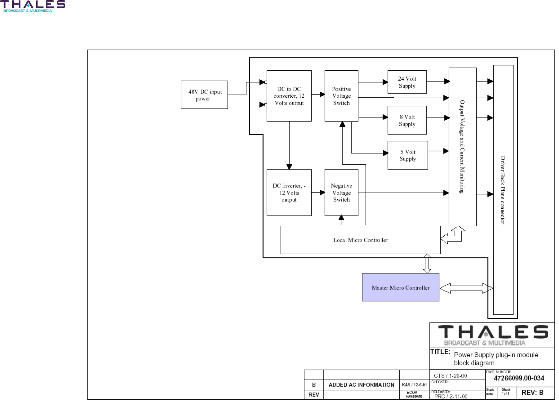
11.1 Power Supply Plug-In Module
The Power Supply Plug-In Module provides the required DC voltage levels for the various
transmitting system assemblies. The Front-End DC Power Supply Module provides the 48VDC
source required for the operation of the Power Supply Plug-In Module.
The Power Supply Plug-In Module contains a DC converter board that converts 48VDC to the
output voltage levels used for the various circuits within the Driver Section and transmitter
assemblies. The Power Supply Plug-In Module generates +24VDC, +12VDC, +8VDC, +5VDC,
and -12VDC. The enable logic of the controller directs the on and off functionality of the +24VDC,
+12VDC and +8VDC supplies. The -12VDC and +5VDC supplies are independent and not
switched by the positive enable logic.
+12VDC: A DC-to-DC converter within the Power Supply Module transforms the 48VDC to
12VDC. The 12VDC supply is fuse protected. The 12VDC supply is filtered on the output to
attenuate ripple from the input source and DC-to-DC converter. An LED located on the front
panel of the Power Supply Plug-In Module confirms the DC-to-DC converter operation. This DC-
to-DC converter provides all of the remaining power requirements of the Driver. The converter is
mounted underneath the DC converter PCB, and directly onto the extrusion. This extrusion
facilitates the thermal dissipation of energy from the DC-to-DC converter.
A positive voltage enabled switch controls the application of +12VDC to the remaining plug-ins
within the Driver. Additionally, the positive voltage enabled switch controls the application of the
12VDC to the 24VDC, and the +8VDC power supplies. These supplies also provide the
operational power to the rest of the system.
+24VDC: A switching power supply steps-up, filters and regulates the 12VDC to generate the
24VDC. Diodes protect the regulator from reverse and over-voltage load conditions. The output
of this power supply is fused to prevent damage to the power supply circuit during transitional
overloads. Since the positive voltage enabled switch controls the supply voltage to this power

Driver Section - 80 -
®
Affinity LBD-200C-N1 Transmitter
Product Manual
supply section, the output voltage will shut down when commanded by the microcontroller. The
output of this power supply section is only used to power the remote interface circuitry on the
user interface module in the exciter.
+8VDC: A linear regulator provides the +8VDC from the +12VDC power supply section. This
regulator is filtered to clean any AC component coupled across/induced from the regulator.
Diodes protect the regulator from over-voltage and reverse-voltage load conditions. A resetable
fuse further protects the regulator during overload conditions. Since the positive voltage enabled
switch controls the supply voltage to this power supply section, the output voltage will shutdown
when commanded by the microcontroller. The output of this power supply section is only used
within other sections of the Driver.
+5VDC: A linear regulator provides a +5VDC output from the +12VDC power supply section. This
power is used with the Power Supply Plug-in for powering the digital monitoring circuits of the
power supply plug-in, and the Master Control Interface (MSI). To assure continuous operation of
the controlling circuitry, this voltage is not controlled by the positive voltage enable.
-12VDC: A switching power supply converts voltage from the +12VDC supply to approximately –
16VDC. This voltage level is filtered and regulated to -12VDC. Diodes protect the regulator from
reverse and over-voltage load conditions. The output of this power supply is fused to prevent
damage to the power supply circuit during transitional overloads.
Similar to the +12VDC power supply section, a negative voltage enabled switch controls the
application of -12VDC to the remaining plug-ins within the Driver.
Power Supply Enable: The positive and negative power supplies work identically, with the
exception of the direction of current flow and type of MOSFET transistor switching the power to
the system. TTL logic from the embedded controller is applied to NPN transistors that supply
sufficient current to drive optocouplers.
The optocouplers have a Darlington-pair transistor drive that when enabled, create a current
draw from the supply voltage, across two resistors, through the optocoupler and ground. This
current draw across the resistors provides a voltage drop.
A tie-point in between the resistors takes the difference in potential to the gate of the transistor.
The difference of potential between the source and drain causes the MOSFET to conduct,
turning on the voltage to the rest of the circuitry behind the switch.
When there is no current flow across the resistors (when the optocoupler is not conducting),
there is no current flow through the resistors, no voltage drop across the resistors, and the
potential from the gate to source remains the same. The MOSFET will not conduct and will
switch off the power to the remaining circuitry behind the transistor.
Current and Voltage monitoring: Current sampling is accomplished by measuring the voltage
drop across a resistor in series with the load. The voltages from both sides of the resistor are
scaled down in order to keep the measured voltages from the supply voltages of the operational
amplifiers. The voltage differences are buffered and applied to an operational amplifier
configured to measure the difference of the two input voltages.
The output of the differential amplifier is applied to a non-inverting amplifier to increase the
voltage near the middle of the system controller 5-volt analog-to-digital converter range. An
integrated circuit containing Zener and Shottkey diodes protect the inputs of the system
controller. The system controller compares this value against previously calibrated values to
determine if the power supply is operating outside of specified parameters.
Driver Section - 81 -
®
Affinity LBD-200C-N1 Transmitter
Product Manual
The input buffers for the current sampling provides the voltage samples. Dividing resistors scale
down the buffer outputs. This provides a sample voltage to the analog-to-digital converters that
is mid-range between 0 and 5 volts.
All of the power supply sections operate in a similar manner. The -12VDC power supply section
uses inverting amplifiers (instead of buffers) with unity gain to convert the sample values to
positive representations of the sampled voltages.
The current and voltage sample outputs are applied to an analog multiplexer integrated circuit.
This chip selects the group of signals that are applied to the microprocessor from a control
provided from the microprocessor.
An onboard Master Control Unit (MCU) with programmable firmware provides monitor and
control functionality. The MCU monitors the voltages and current from the power supply and
controls the output based on reference measurements. The MCU will switch off positive
voltages to the Driver Section when a loss of negative voltage is detected. This feature protects
the amplification devices located within the Upconverter and Power Amplifier modules.
The Power Supply Plug-In Module controller routes RS-485 multi dropped network
communications to other modules on the network.
A temperature sensor within the Power Supply Plug-In Module provides input to the
microcontroller proportional to the ambient temperature of the module. If the Power Supply
Plug-In Module operates over the temperature specification, a controlled shutdown of all
supplies will occur.
The Power Supply module contains an RS232 interface located on the front panel. This EIA
standard interface allows for connectivity with a serial host such as a desktop computer.
The Power Supply Plug-In Module is “Hot Swap” compatible allowing for module replacement
without the need of powering down the module or transmitter.
NOTE: During the “Hot Swap” process as the Power Supply Plug-In Module is removed, the
transmitter will go off air until the replacement Power Supply Plug-In Module is plugged back
into the chassis.
The Power Supply Plug-In Module is cooled by a single fan and is mounted in an extrusion that
is designed to dissipate the heat generated from the components within. The fans of the Sub-
Chassis also ventilate the Power Supply-Plug-In Module.

Driver Section - 82 -
®
Affinity LBD-200C-N1 Transmitter
Product Manual
11.1.1 Power Supply Plug-In Module Specifications
Parameter Specification Notes
Input
Input voltage 48VDC
Input current 4 amps, maximum Low line @ full rated power
Peak inrush current 6 amps
Efficiency 85% typical Full load
Output
Main Output
12VDC ± .5
+8VDC ± .5
+24VDC ±.5
-12VDC ±.5
All voltages are fixed
Output current Main Output
+12V @ 3.5 amps
+8V @ 3.0 amps
-12V @ 0.185 amps
+24V @ 0.240 amps
Output supply interruption will
occur during overload conditions
Output power Main Output
+12V @ 42 watts
+8V @ 24 watts
-12V @ 2.2 watts
+24V @ 5.8 watts
Output supply interruption will
occur during overload conditions
Ripple & noise 200 mv pp 20 MHz BW
Load regulation .4% no load to full load
Protection
Over voltage Power supply will shut down if
voltage exceeds nominal voltage
by 20%
Over current Power supply will shut down if
current exceeds maximum value
Over Temperature Power supply will shut down if
temperature exceeds 70°C.
Restart is automatic when power
supply returns to normal
operating temperature. If over
temperature condition occurs
twice, power supply will latch in a
shutdown condition.
Output voltage

Driver Section - 83 -
®
Affinity LBD-200C-N1 Transmitter
Product Manual
Power input interlock All voltage outputs are disabled
when a negative supply is
overloaded to prevent damage to
equipment.
Internal Fuse (F1) Thales P/N 750082-01
Power Supply Plug-In Module Specifications (cont.)
Environmental
Cooling Forced air-cooled, minimum of 8 CFM required Forced air-cooled
drawing ambient air
through the intake on
the front of the power
supply and exhausting
out the rear.
Operating temperature 0° to 50° C
Relative humidity 0 to 95% non-condensing
Alarms/Indicators/Adjustments/Controls
DC output failure alarm TTL Low=DC output failure Signal available at
backplane
DC OK indicator A lit Green LED=DC is within tolerance Visible via front panel
Agency Compliance
Safety Meets UL and CSA approvals Pending
Physical
Weight 4.5 lbs (2.04 Kg)
Front panel color Matches Sherwin William’s Paint#:
Light gray-F63TXA2555
Paint mix number 4303
identifies store locations
when added to paint
number
Lexan overlay color
matched as indicated.
Mechanical dimensions 4.75”H x 3.0”W x 17.5” D
(12.07cm H x 7.62cm W x 44.45cm D)
Power Supply Firmware P/N
(Programmed onto 47266096 DC converter board)
File name
47266093.01-525 PWRSUP1_1.s19
Driver Section - 84 -
Affinity® LBD-200C-N1 Transmitter
Product Manual
Driver Section - 85 -
Affinity® LBD-200C-N1 Transmitter
Product Manual
Driver Section - 86 -
®
Affinity LBD-200C-N1 Transmitter
Product Manual
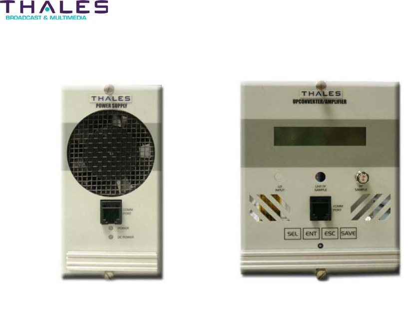
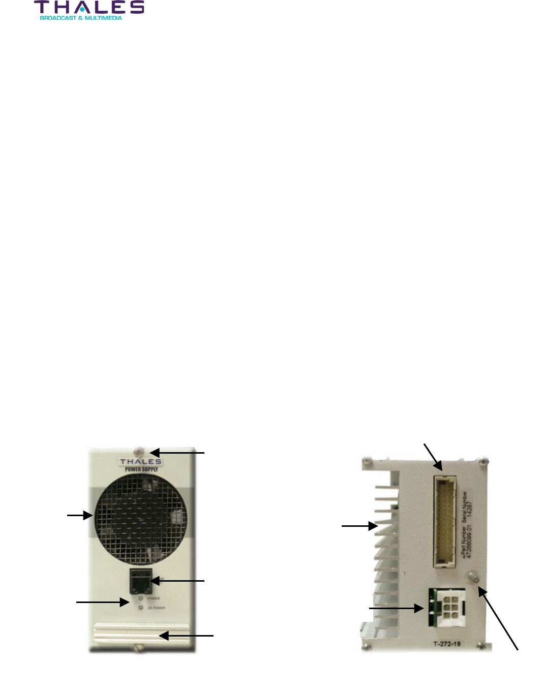
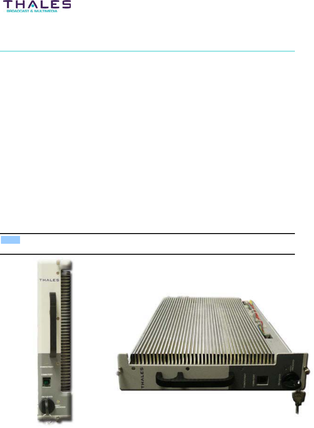
11.1.2 Power Supply Module Front and Rear Panel Descriptions
Thumbscrews: This hardware secures the module to the sub-chassis and provides a reliable
ground connection. Loosen to remove the module for replacement or repair.
Fan: An 18-CFM VDC fan used for plug-in module cooling.
Communication Port: The RS-232 serial communication port is used for setup and
diagnostics.
Power LEDs: The Power LEDs are a visual indication used for status monitoring of the
operating power parameters.
x Power: Green indicates power from the Front-End Power Supply. An unlit LED
indicates no power from the Front-End Power Supply.
x DC Power: Green indicates Power Supply Plug-In Module output voltage is present.
An unlit LED indicates no output power from the Power Supply Plug-In Module.
Handle: The handle assists in removing the Power Supply from the sub-chassis.
Heatsink: The heatsink aids in heat dissipation generated within the Power Supply.
Power Connector: The 6-pin header power connector is used to input power from the Front-
End Power Supply.
48-Pin DIN: The 48-pin DIN connecter is an interface point to the backplane (power, control,
and diagnostics).
Ground/Alignment stud: The Ground/Alignment stud ensures proper grounding is achieved,
and aids in the alignment of the Power Supply module within the sub-chassis. The stud also
ensures that circuit grounding is made before the engagement of the 48-pin DIN connector.
Front Panel Rear Panel
Handle
Communication Port
Power LEDs
Fan
Thumbscrew
Power Connector
Ground/Alignment stud
48-pin DIN
Heatsink
Driver Section - 87 -
Affinity® LBD-200C-N1 Transmitter
Product Manual
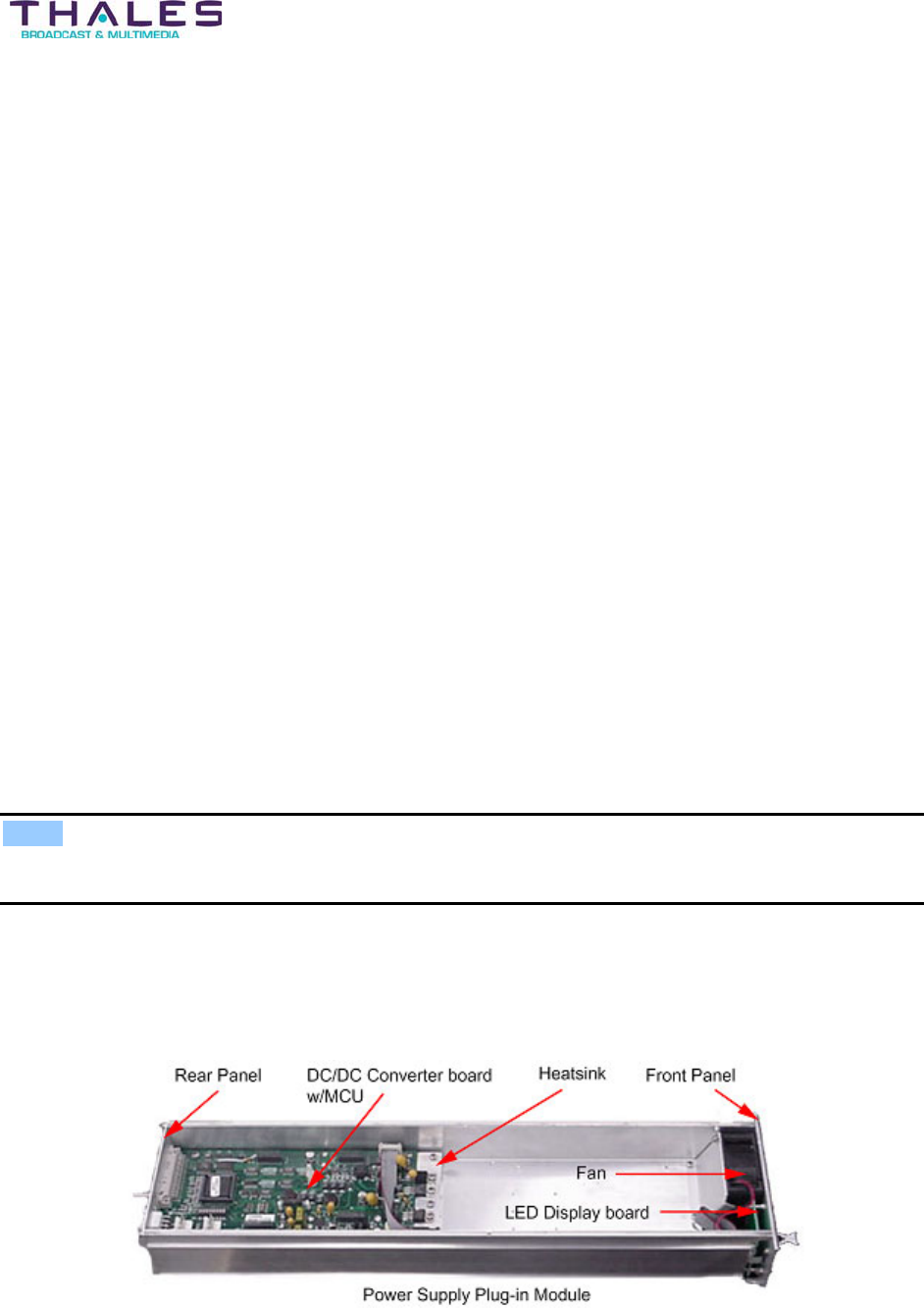
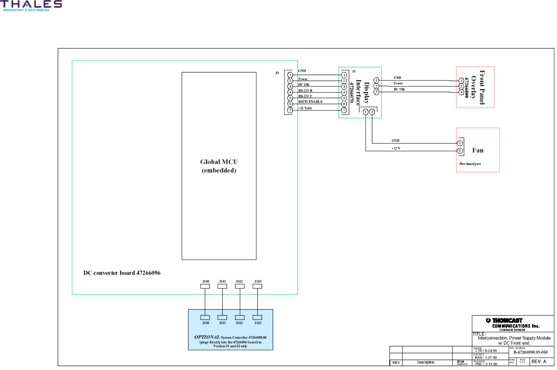
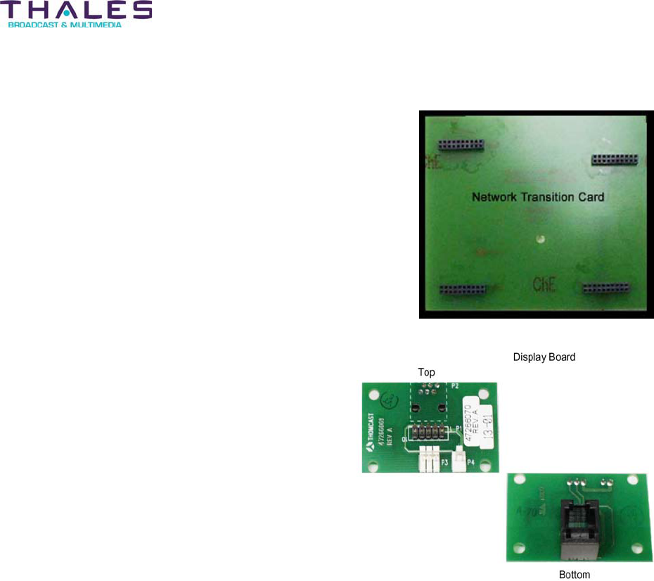
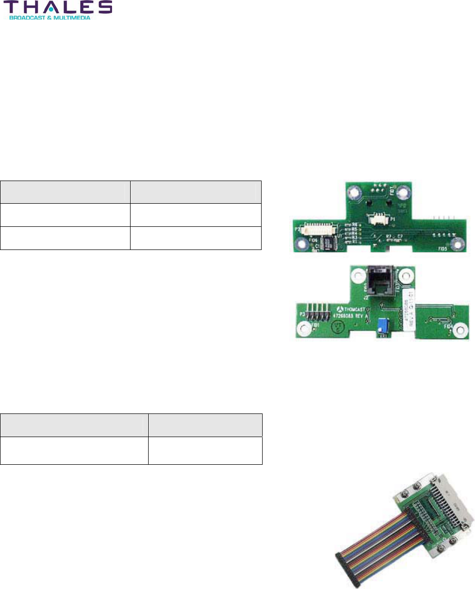
Network Transition Card
The power supply module, like all modules within the
Affinity chassis and Ancillary rack, are networked through
an RS-485 network.
This Printed Circuit Board (PCB) is housed within the
Power Supply plug-in module, (only specific versions) in
systems where network management is located outside of
the plug-in module. The sole function of this board is to
route the RS-485 signals directly from the Remote RS-485
buss on the rear panel connector directly to the DC
Converter PCB.
Display Board
The display board routes the LED display signals
to the DC converter board, supports the front
panel communications port, routes the
communications signals to the DC converter
board, and provides power to the front panel fan.

Driver Section - 88 -
®
Affinity LBD-200C-N1 Transmitter
Product Manual
11.2 Upconverter Module
The Upconverter Module is a plug-in assembly mounted within the Driver Section of the
Affinity®. The basic function of the Upconverter Module is to convert and amplify the exciter
output to the proper power level required to drive the subsequent final amplification stage. To
accomplish this, the appropriate level IF signal, local oscillator signal(s), and power supply
voltages must be present on this plug-in.
The Upconverter performs ALC on the RF signal maintaining a constant drive level after the first
conversion stage. The Upconverter Module is attached to the main chassis via three slide-rails
and two thumbscrews. Several internal assemblies make up the Upconverter Module including:
x Microcontroller Unit (MCU)
x Front panel board
x Distribution board
x ALC Module
x Converter Sub Module
x Band Pass Filter
x Temperature Sensor Board
x Intermediate Power Amplifier
x Connector Interface
x LCD board
These internal boards are accessible through two detachable covers. The covers, together with
the rear panel Fan Assembly, are part of the forced-convection cooling system.
Theory of Operation
RF signals are sent to and from the Upconverter Module through coaxial connectors and cables
on the back panel. Power and communication signals go through a 48-pin connector interface
located on the rear panel. RF signal is delivered to the internal modules of the Upconverter via
coaxial cables utilizing floating connectors. Signal traffic other than RF, such as power supply
voltages, detected power voltages, and serial data from the Microcontroller Unit, are distributed
between the modules using the Distribution board and connecting harnesses.
The Microcontroller Unit (MCU) contains firmware that controls and monitors the top-level status
of the transmitter, and indicates status of the Driver Power Supply and Upconverter modules,
and the transmitter forward and reflected power. The MCU provides an interface to the Front
panel board switch assembly and the LCD board. The switch assembly is used to scroll through,
and enter the user-interface options. The front panel switch assembly (keypad) has limited
ability to make system or Upconverter module control functions; main calibration is done via the
RS-232 port on the Upconverter. The LCD assembly provides a visual status of the menu
navigation. The UHF signal from the output of the exciter is delivered to the UHF input of the
Upconverter and then routed to the Converter sub-module.
Driver Section - 89 -
Affinity® LBD-200C-N1 Transmitter
Product Manual
UHF – IF Upconverter sub-module
The UHF– IF Upconverter sub-module is responsible for amplifying, filtering, and in conjunction
with the second LO which enters the rear of the module, upconverting the UHF input signal. The
module houses a single upconverter board, which besides the upconverter function, has a
voltage variable attenuator for performing ALC, a detector for sensing UHF input presence, and
a sample for front panel monitoring.
The synthesizer module within the Sirius DVB-H assembly is responsible for producing the two
Local Oscillator (LO) outputs. In the following figure, application of the LO is shown. The first LO
is mixed with an intermediate frequency (IF) that is filtered to produce a second IF. This LO will
also determine the output spectrum orientation by utilizing high or low band conversion in this
stage. The second IF frequency is heterodyned with the second LO resulting in the final output
frequency. In single conversion applications the first LO is not required.
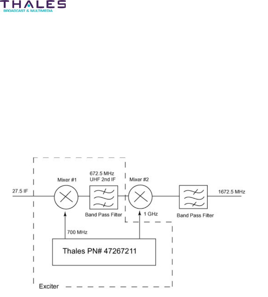
Inside the module, the UHF input signal enters the upconverter board where it is filtered and
then mixed with a 1GHz LO to produce an RF signal at 1672.5MHz. The LO signal used in the
upconversion is generated by the synthesizer within the Thales exciter. The LO frequency is
fixed and the actual channel is set by the incoming UHF frequency, for example, if the UHF is
672.5MHz the LO will be 1000MHz. This means no frequency inversion will occur in the second
conversion stage. The up-converted UHF signal is bandpass filtered to attenuate unwanted
mixing products. A notch filter provides additional attenuation to the LO.

Driver Section - 90 -
Affinity® LBD-200C-N1 Transmitter
Product Manual
Intermediate Power Amplifier (IPA) sub-module
After exiting the ALC module the signal is amplified by 13 dB by the IPA. The IPA Sub-Module
contains a temperature sensing circuit that outputs to the MCU, via the Distribution board,
voltage levels that are proportional to the temperature of the upconverter plug-in. The final RF
signal exits the rear of the upconverter plug-in.
ALC Sub-Module
The ALC Sub-Module located internally in the Upconverter Module, containing both integrator
and Positive Intrinsic Negative (PIN) attenuators, uses a closed-loop level controller to
compensate for PA Module gain variation, and regulates overall output power. The closed-loop
level controller works by receiving voltage samples from the output of the Envelope Detector
Module proportional to the transmitter output power, comparing this voltage to an internal
reference, and adjusting the gain to compensate for PA Module output gain variation. This
compensation ensures the transmitter power level remains constant. Indication of forward and
reflected power levels of the transmitter and forward power level of the Upconverter module are
displayed on the LCD assembly once information originated in respective power detection
modules are routed to, and then processed by, the MCU.
The Connector Interface board provides +12, -12, and +8VDC to the respective sub-modules
and routes forward and reflected detected power voltages for further processing. This board is
also the conduit through which serial data is exchanged between the Upconverter Plug-In
Module and the rest of the system.
Temperature Sensor board
Receives voltage proportional to the temperature generated by a temperature sensor typically
placed on the last power amplification stage.

Driver Section - 91 -
Affinity® LBD-200C-N1 Transmitter
Product Manual
The Front panel PCB has a serial port that can be used for testing, adjusting or controlling
most of the plug-in functions. A personal computer and application program is required to
accomplish this task. The front panel keyboard and display board provide a user interface
capable of controlling a limited number of functions inside the Upconverter, and for the
presentation of a series of measurements in the LCD display. See Table below for a list of user
interfaces.
Menu display Description
Greeting Displays “Thales Broadcast & Multimedia”
State Control
Mode Local/Remote
Operate State On-Air/Standby
System Status Displays the Upconverter Module status
Power Supply Status Displays the top level status of the Power Supply
Plug-In Module
Upconverter Module “In Signal” Displays the ON/OFF status of “In Signal”
Upconverter Module “System Forward Power” Displays the value of “System Forward Power” in
percentage
Upconverter Module “System Reflected
Power”
Displays the value of the “System Reflected Power”
in percentage
Upconverter Module “Forward Power” Displays the value of the Upconverter Module
internal “Forward Power” in percentage
List of User Interfaces
Driver Section - 92 -
Affinity® LBD-200C-N1 Transmitter
Product Manual
Upconverter Module Architecture

Driver Section - 93 -
®
Affinity LBD-200C-N1 Transmitter
Product Manual
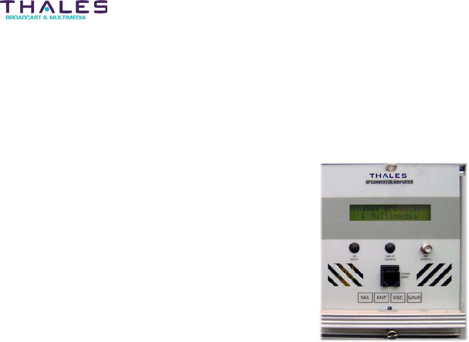
11.2.1 Upconverter Plug-In Module Specifications
Parameter Specification Test Conditions/Notes
IF Input
Digital
Average Input Power -15dBm ±3 dB 2²³-1 PN data sequence (at
transmitter output)
Input Frequency 672.5MHz
Connector/Impedance Blind Mate/50ȍMates with floating back-plane
connector
RF Output
Digital
Average Output Power 20mW to 200mW Function of A.L.C. settings-2²³-
1PN data sequence (at driver
output)
Output Frequency 1672.5 MHz
Frequency Response ±0.25 dB Fc±4 MHz
Measured at sub-rack output
IM³(dBc) <50 20dBm RF output power
(64QAM; COFDM) Relative to in-
band average PSD measured @
100 KHz RBW
Carrier to Noise (C/N) <55dB
Hum and Noise <-60 dBc
Group Delay ±20ns Fc± 4 MHz
Digital Modulation
Error Vector Magnitude (EVM)
<2.0% 64-QAM/8-VSB @ 5.06 Msps
RMS average over 12,500
symbols Measured at Sub-rack
output
Digital Modulation
Signal to Noise Ratio (SNR)
<35dB 64-QAM/8-VSB @ 5.06 Msps
RMS average over 12,500
symbols Measured at sub-rack
output
Magnitude Linearity
(AM-AM conversion)
±0.125dB Measured at sub-rack output
Phase Linearity
(AM-PM conversion)
±0.75qMeasured at sub-rack
RF Output Regulation r0.2dB Measured at Sub-rack output
Connector Impedance Blind Mate 50:Located at the back panel of the
plug in. Mates with floating back-
plane connector

Driver Section - 94 -
®
Affinity LBD-200C-N1 Transmitter
Product Manual
Front Panel Samples
Sample Name Coupling Factor
2nd IF Sample -45+/ -2 dB Front Panel access through an
SMA 501 Female Connector
Loaded with 501 termination
when not is use
RF Sample 470 MHz
860 MHz
-30+/-4 dB Front Panel access through an
SMA 501 termination when not
in use
DC Power Requirements
Voltages/Current +12VDC .5 @ 2.8A max
+8VDC .5 @ 1.0A max
-12VDC .5 @ 150ma max
Connector 48 conductor, 3amps/circuit
minimum
Interfaces to back-plane
Environmental
Cooling Forced air-cooled, minimum of 18
CFM required
Forced air-cooled drawing
ambient air through the intake on
the front of the Pre-Amplifier
Plug-In Module and exhausting
out the rear of the module
Operating Temperature 0qC to 50qC
Relative Humidity 0 to 95% non-condensing
Alarms Indicators/Adjustments Controls
RF Output Failure Alarm DRIVER FAILURE Low (TTL
Low)=RF Output Failure
Signal available at back-plane
Over Temperature Alarm DRIVER FAILURE Low (TTL
Low)=Over Temperature
Signal available at back-plane
In Signal Indicator YES (when present) or NO (when
absent)
Visible via LCD Display
Transmit Indicator XMIT (when RF power is
present) or No Pwr (when RF
power reads 0%)
Visible via LCD Display
Power Supply
Status/Measurements
PASS or FAIL/ V scale Visible via LCD Display
RF Power Measurements % Scale Visible via LCD Display

Driver Section - 95 -
Affinity® LBD-200C-N1 Transmitter
Product Manual
Parameter Specification Test Conditions/Notes
Input Level Control RS-232 interface
Frequency Response (low side)
Control
RS-232 interface
Frequency Response (high side)
Control
RS-232 interface
ALC Level Control RS-232 interface
Stand-by Control RS-232 interface
Reset Control RS-232 interface
Environmental
Operating Temperature 0 to 50q C Guaranteed operation over
temperature range
Relative Humidity 95% non-condensing
Physical
Mechanical Dimensions 4.75”H x 4.2”W x 17.5” D
Approximate Weight 5 lbs (3Kg)
General
Front Panel Color Matches Sherwin William’s Paint
No.
Light Gray F63TXA2555
Medium Gray F63TXA4841
Paint mix number 4303 identifies
store location when added to
Paint No. Lexan overlay color
matched as indicated

Driver Section - 96 -
®
Affinity LBD-200C-N1 Transmitter
Product Manual
11.2.2 Upconverter Internal Interconnect Drawing
Insert 47266889-050 Upconverter interconnect drawing

Driver Section - 97 -
®
Affinity LBD-200C-N1 Transmitter
Product Manual
11.2.3 Upconverter RF Block Diagram
Insert 47266889-034 RF block Diagram
Driver Section - 98 -
®
Affinity LBD-200C-N1 Transmitter
Product Manual
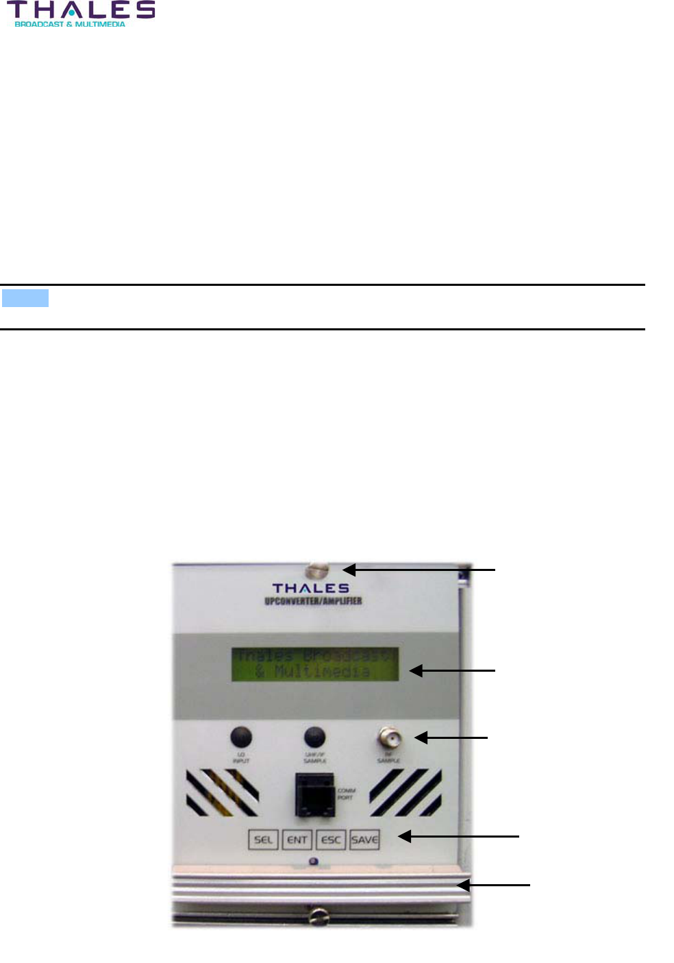
11.2.4 Upconverter Module Front and Rear Panel Description
Front Panel
Thumbscrews: This hardware secures the module to the sub-chassis and provides a reliable
ground connection. Loosen to remove the module for replacement or repair.
Liquid Crystal Display (LCD): The LCD displays a series of measurements, user adjustments,
and general status information.
RF Sample: The RF Sample port is a female SMA 50: connector used to test the output level.
NOTE: The RF Sample contains pre-distortion and is not representative of output signal. The
RF sample is a reference point for testing only.
RS-232 Communication Port: The Communication port is an EIA standard RS-232 port used
for communicating with a PC.
Keypad: The Upconverter Keypad assembly contains user selection keys.
SEL: Select provides the user with scrolling capabilities.
ENT: Enter allows the user to choose an option.
ESC: Escape allows the user to go back to the previous screen
SAVE: Save allows the user to store new settings or adjustments
Handle: The Handle is used to assists with the removal of the module from the Sub-Chassis.
Thumbscrew
Liquid Crystal Display
RF Sample
Keypad
Handle
Upconverter Plug-in Module Front View
Driver Section - 99 -
®
Affinity LBD-200C-N1 Transmitter
Product Manual
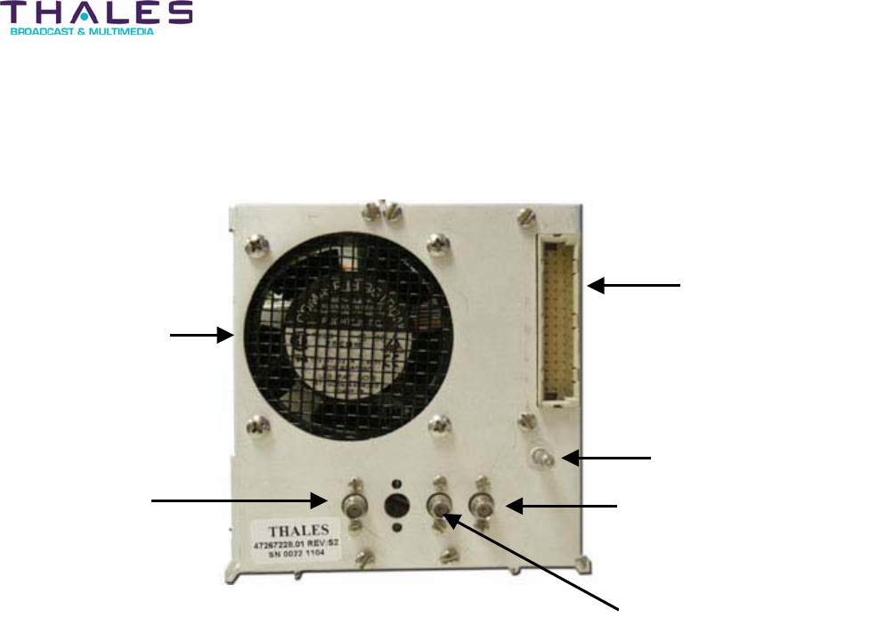
Rear Panel
48-pin DIN
Ground/Alignment stud
IF Input
LO#1 Input
RF Output
Fan
Upconverter Plug-in Module Rear View
FAN: The 18 CFM Fan assembly is used as a cooling device for the Upconverter Module. The
Fan is powered by DC voltage.
48-PIN DIN: The 48-pin DIN connector is an interface point to the Driver Section backplane that
includes the power, control, and diagnostics functions of the Driver.
GROUND/ALIGNMENT STUD: The Ground and Alignment Stud ensure proper electrical
grounding is achieved before engaging the 48-pin DIN connector. It also aids in the alignment of
the module within the Sub-Chassis.
IF INPUT: Male 50: blind mate provides interface to the backplane and allows passage for the
IF input signal from the exciter.
LO#1 INPUT: Male 50: blind mate provides interface to the backplane and allows passage for
the LO#1 input from LO Plug-In
RF OUTPUT: The RF Output is a male 501 blind mate connector that is used to supply the RF
output signal to the Power Amplifier Segments.
Driver Section - 100 -
®
Affinity LBD-200C-N1 Transmitter
Product Manual
11.2.5 Upconverter Module Power-On Sequence
When power is applied to the Upconverter Module, a display test is performed. The front panel
of the LCD is illuminated for approximately one second then extinguished. This sequence
provides verification that the front panel LCD and MCU logic is functioning. Upon completion of
the display test, the LCD will display the Upconverter Module status as determined by the
firmware tests.
Navigating the front panel assembly:
THALES BROADCAST & MULTIMEDIA is the default display
To view the status of the system and each plug-in module, press
the SEL button as many times as necessary.
Press SEL once=Local/Remote Mode
Press SEL once = Status menu
Status=Xmit, Fail or NoPwr
Press ENT once to enter the TX Control state
Press ENT or SEL to choose Xmit or Stdby or ESC to Quit to
Status Menu
Press Save to store chosen state of operation; TX enters state
then exits to Status menu.
From Status menu; Press SEL once=Power Supply
Status=Pass or Fail
From Status menu; Press SEL twice =Local Oscillator
Status=Pass or Fail
From Status menu; Press SEL three times = Upconverter
Status=Pass or Fail
Press ENT to examine lower level parameters, ESC to return to Upconverter menu
Press SEL four times=Back to Power supply. From this point, pressing SEL will scroll through
the list again.
When at the desired Upconverter status, press ENT followed by SEL as many times as
necessary to view additional information about the plug-in module parameters.
The first ENT=[In Signal]
Yes or No
Press SEL once= [System Fwd Power]
Power=100
Press SEL twice=[System Ref Power]
Power = 0
Press SEL three times=[Upconv Fwd Power]
Power=100
Press SEL four times=[Back to In Signal]
Driver Section - 101 -
®
Affinity LBD-200C-N1 Transmitter
Product Manual
From this point, pressing SEL will scroll through the list again.
At any point to exit and return to the default display, press the ESC key as many times as
necessary.
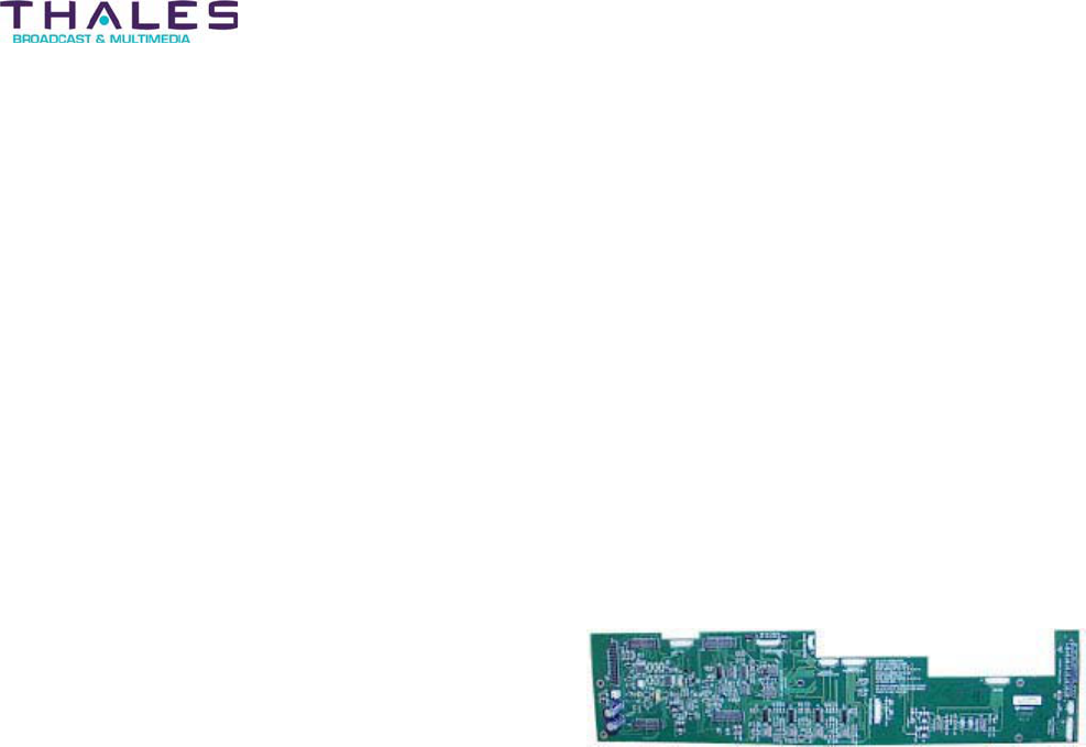
Distribution Board
The Distribution board consists of a 14-1/4” x 3-1/2” circuit board that is screwed to the
Upconverter chassis. The circuitry on this board permits the processing of signals, and the
control over the flow between the Upconverter plug-in IF/RF modules and the microprocessor
board, the front panel through connector J2, and the display boards through J6. The Distribution
board and Interface board, via connector J1, allow communication between the Upconverter
Plug-In Module and the Backplane board. The module is divided into two parts: digital
processing and analog processing.
Digital Processing Circuits
U3 (when present), U4, U6, U8, U9, U10 and U11
and related passive components form the digital
portion of this module. An extension of the
microprocessor board capabilities would sufficiently
classify their function.
Analog Processing Circuits
All components, other than those listed above, are classified as the analog-processing block.
Amplification and flow control of signals, as well as sensing of current and power levels, are the
main tasks performed by these components.
Working principle
After powered up, the Distribution board starts receiving commands from the microprocessor via
connectors J100-J103. One-by-one the voltages needed to control the IF/RF modules are set to
a pre-working level. IF AGC reference, IF threshold, IF equalization, RF ALC reference,
reflected power threshold, and power limiter voltages are set through the D/A converters U6,
U8, U9 and U10 as well as the operational amplifiers U13, U14, U15 and U16. The commands
originating from the microprocessor board are processed and delivered to Q3 and Q4, which
turn on the GaA medium power devices present in the UHF Driver Amp assembly and IF-UHF
sub module (if present).
Voltages proportional to the current drawn by the UHF Driver Amp assembly are generated by
sampling resistors R74, R75 and R77 and delivered to the microprocessor. Resistors R83, R84
and R85 send the current consumption information of the IF-UHF sub module. External or
internal power level information of the plug-in is processed by U5 to either: generate power
measurement voltages, or generate ALC voltage at U7 pin 4. Temperature proportional voltage
is routed from the UHF Driver Amp assembly, through J11, to the processing board. All voltages
proportional to current values or power levels are forwarded to the microprocessor board. With
these voltages, pass or fail conditions and measurements can be displayed or reported to the
MSI controller module by the microprocessor board (See additional documentation on the MSI

Driver Section - 102 -
®
Affinity LBD-200C-N1 Transmitter
Product Manual
circuit description). Besides helping the processor card monitor the status of the IF/RF modules,
the distribution board also routes data from the front panel board (specifically the RS-232 port
and keyboard switches) and data to the LCD module.
Specifications
Parameter Specification Notes
Power Supply Requirements
+8V r .3V @ 1.1A (max)
+12V r .5V @ 2.5A (max)
-12V r .5V @ 100mA (max)
+24V (not used)
All 47266889 module loaded
Operating Temperature 0qC to 50qC
Control Signals Voltages (part A)
AGC_MAN_CTL
AGC_AUTO_CTL
IF_THRESHOLD_CTL1
PWR_LIMIT
ALC_MAN_CTL
ALC_AUTO_CTL1
d.02 V to t9.2 V
Voltages measured at
connectors providing signals to
respective modules
Control Signals Voltages (part B)
FREQ_RESP#1
FREQ_RESP#2
d.05 V to t10.5 V Voltages measured at
connectors providing signals to
respective modules
Filtered Fan noise .02 Vpp. max Measured at J11
Driver Section - 103 -
Affinity® LBD-200C-N1 Transmitter
Product Manual
Front Panel Driver Board Description
The Front Panel Driver Board acts as an interface between the Upconverter front panel and the
Distribution board. This board features an RS-232 port, which utilizes a telephone type (RJ11)
phone jack connector. Serial port signals are routed through the board to the Distribution board.
Also present on this board is a de-bounce circuit that processes the front panel soft keypad
strokes.
Parameter Specification
Power supply 5V @ 10 mA
Connectors Serial Port RJ11
Connector Interface Board Description
The Connector Interface Board is used to connect the 48-pin connector, located on the back
panel, to the two 26-pin connectors located on the Distribution board.
Parameter Specification
Maximum current per
connector 2A @ 80º C
UPS System Description - 104 -
®
Affinity LBD-200C-N1 Transmitter
Product Manual
12 UPS System Description
Pending
Downconverter Module - 105 -
®
Affinity LBD-200C-N1 Transmitter
Product Manual
13 Downconverter Module Description
Pending
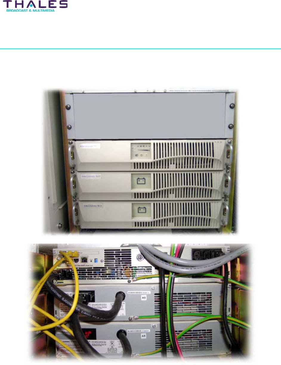
Power Amplifier Module - 106 -
®
Affinity LBD-200C-N1 Transmitter
Product Manual
14 Power Amplifier Module Description
The Power Amplifier (PA) Module amplifies the inputted Driver signal to the power level
required for transmission. The PA Modules operate in tandem with other PA Modules to obtain
the required power level for the transmitter. The PA Modules are plugged into the backplane of
the Sub-Chassis assembly and operate in an RS-485 multi-drop environment. Each module
contains a unique logical address that allows for operation, control, and monitor activities within
the transmitter system. An RS-232 port located on the front panel of the PA Module is provided
for module setup, historical record extraction, and diagnostic feedback. A POWER/FAULT
status indicator and the ON/LOCKED, OFF/UNLOCKED key assembly is also located on the
front panel of each PA Module. The key-lock assembly provides physical and electrical
connection.
Operational power required by the PA Module is derived from the Front-End Power Supply. This
48VDC drives the voltage regulators that produce the voltage levels for the analog and digital
circuitry contained within the PA Module.
The diagnostics, operation, and monitoring features of the PA Module are controlled by a
firmware driven microcontroller system.
The PA Modules are “Hot Swap” compatible. Defective PA Modules, accessible from the front of
the cabinet, may be removed and replaced while on-air, and without shutting the entire
transmitter system down.
NOTE: During this procedure an automatic power reduction will occur to ensure transmitter
protection.
Power Amplifier (PA) Module
Power Amplifier Module - 107 -
®
Affinity LBD-200C-N1 Transmitter
Product Manual
The PA chain uses segmented power amplifiers in parallel that are directly interchangeable.
Affinity® amplifiers utilize a design that is optimized for the 1670-1675MHz range. Each
amplifier module is also gain and phase matched for consistent performance from module to
module.
The high gain RF amplifier module uses GaAs FET high reliability transistors that are biased for
class AB operation. The inherent linearity of these amplifiers, and the quality of the associated
correction circuits, combine to product excellent linearity performance. Each final power
amplifier module has protection systems for high temperature and over-current. The final power
amplifier assembly has a protection system for excessive VSWR conditions.
Due to transistor redundancy, the standby arrangements are such that an abrupt and total
shutdown of the transmitter due to failure of one or more transistors is implausible; the same is
true of power supplies.
Block diagram of final RF Power Amplifier
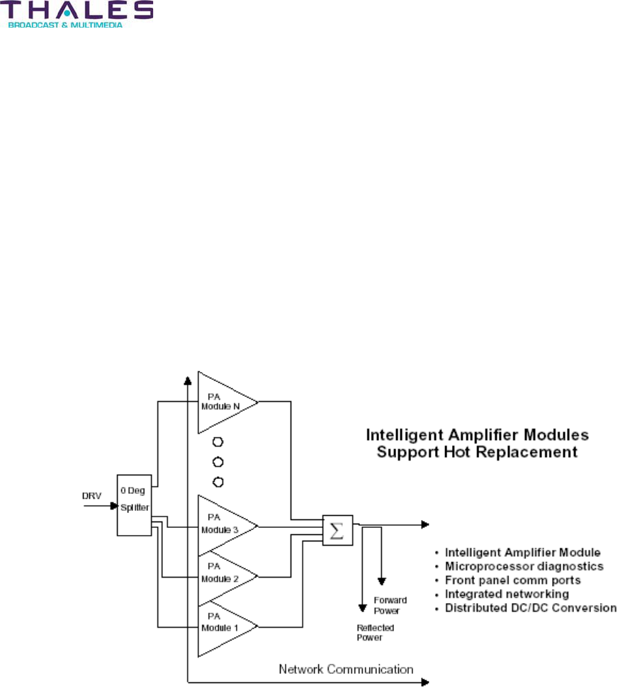
The power amplifier assembly uses “n” number of power amplifier modules in parallel to achieve
the required output power. Amplifier combining is through the very low-loss patented passive
combining system exclusively available from Thales. This combiner technology allows for any
number of amplifier combinations without restriction, which provides flexibility in system design,
and reduces cost by putting power scalability at the customer’s fingertips. Thales also allows the
customer to select the desired margin built into the power amplifier stage; options of 0.3 and 1.5
dB are offered giving cost control options to the system designer. Typically two power amplifier
modules are used to achieve 50 watts, 16 power amplifiers are used to achieve 400 watts
building in 1.5dB margin (or headroom). A controlled soft fail method is applied in the event of a
faulted amplifier(s) safely reducing transmitter power while maintaining on-air availability. Power
reduction ranges from 1.5dB to 6dB and is dependant on the total number of amplifiers in the
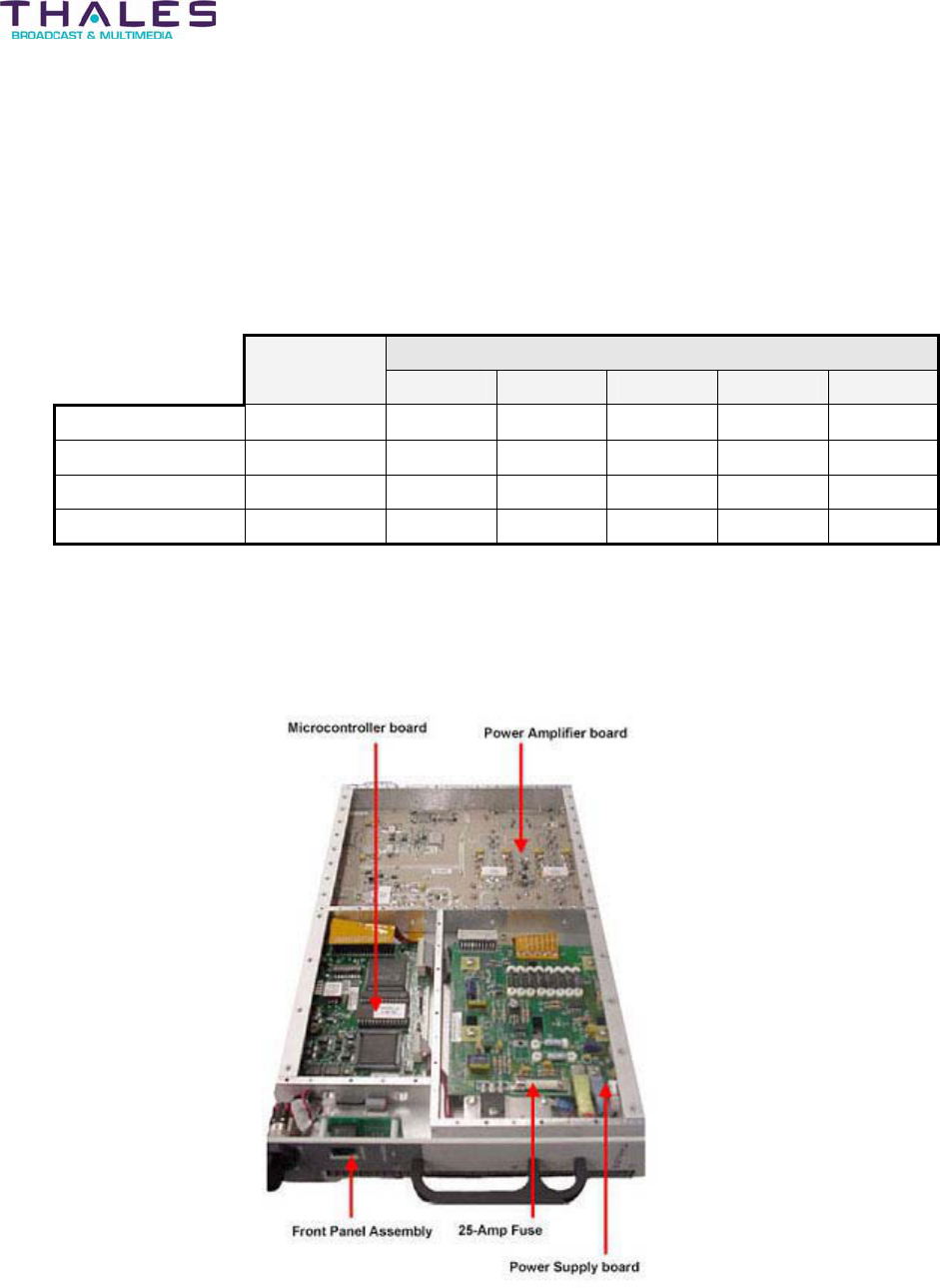
Power Amplifier Module - 108 -
®
Affinity LBD-200C-N1 Transmitter
Product Manual
system verses the number of faulted modules. A transmitter is deemed to be unrecoverable
when the output power has fallen by more than 6dB and a controlled shut down occurs.
The following table (given for example) shows analysis of the consequences of the failure of a
number (from 1 to n) of amplifier modules (theoretical values) for 50 to 400 watt RMS
transmitters.
Number of faulty power amplifiers
“n” number
of amplifiers 1 2 3 4 6 to 8
PA – 400 watts 12 -1.5dB -1.5dB -3.0dB -3.0dB -6.0dB
PA – 200 watts 6 -1.5dB -3.0dB -6.0dB -6.0dB
PA – 100 Watts 3 -3.0dB -6.0dB
PA – 50 Watts 2 -6.0dB
PA Module Layout
The PA Module segment consists of a Power Amplifier board, a Microcontroller board, a Power
Supply board, and a Front Panel board.
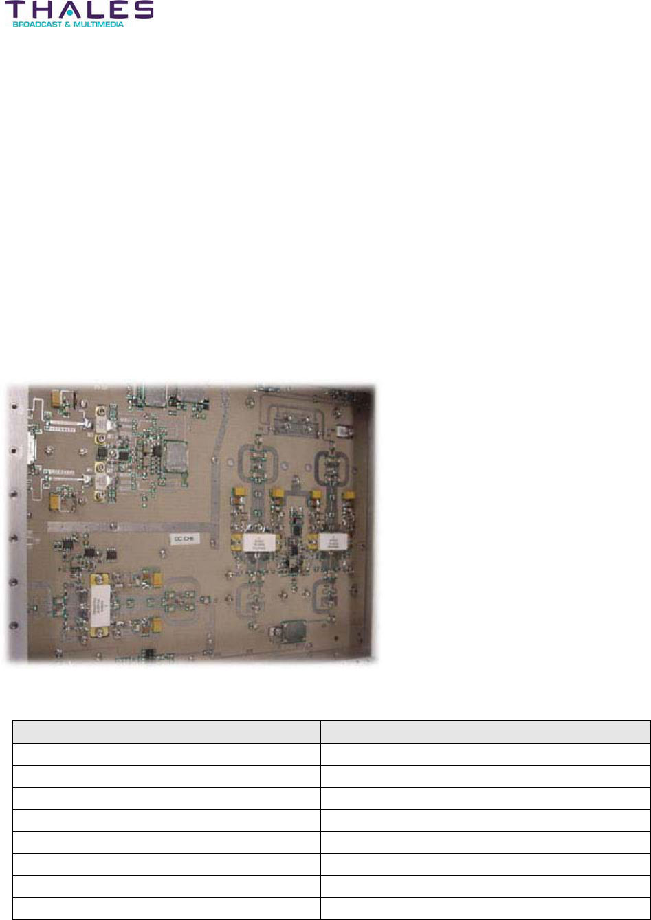
Power Amplifier Module - 109 -
®
Affinity LBD-200C-N1 Transmitter
Product Manual
Power Amplifier Board
The Power Amplifier Board amplifies the RF INPUT signal from the upconverter assembly to the
output power requirement of the transmitter.
The Power Amplifier Board has a high-gain architecture providing 38.5 dB of gain, an output of
1-dB, and compression of 53.5 dBm. The signal passes through a pin diode attenuator that sets
the overall gain of the amplifier. A variable phase shifter sets the overall phase insertion.
In the first stage of the amplifier, a 3-dB hybrid provides a reliable load to the driver and a flat
broadband frequency response to the amplifier. The second and third stages of amplification
efficiently provide the proper output power with a minimum of distortion.
A 3 dB combining system provides for a low output Voltage Standing Wave Ratio (VSWR). The
directional coupler provides a sample signal proportional to the forward and reflected power.
This measurement ensures that the amplifier delivers the correct power. An IC measures the
operating temperature of the amplifier that is monitored by the microcontroller. The amplifier is
placed in a faulted state if the temperature exceeds a limit set by the microcontroller.
Power Amplifier Board Specifications
Parameter Specification
Input Voltage 48VDC
Input Current 19.8 Amps
RF Gain 38.5 dB
Output Power 47 dBm (COFDM signal)
Flatness (BW 392 MHz) ± 0.75 dB
Input VSWR 1: 1.6
Output VSWR 1: 1.5
Operating Temperature 0°to 43°C
Power Amplifier board

Power Amplifier Module - 110 -
®
Affinity LBD-200C-N1 Transmitter
Product Manual
Microcontroller Board
Control and monitoring functions of the PA Module segment is accomplished through the
Microcontroller Board located within the PA Module segment housing. The Microcontroller
Board uses an 8-bit microcontroller unit (MCU) with on-board memory to perform the control
and monitoring functions. The microcontroller board includes analog signal conditioning, A/D
and D/A converters, supply voltage regulation, and serial data interfaces.
Monitoring operations involve collecting analog signals and logic data from the power amplifier
segments. Analog inputs, forward power, reflected power, and temperature, are received from
the RF power amp connector J1. The analog input drain supply voltage (VDD), and high voltage
DC is received from power supply connector J2. Forward power and reflected power inputs are
amplified by operational amplifiers with a gain of approximately two, while temperature, drain
supply voltage, and high voltage DC is buffered by unity gain stages. Following the VDD buffer
stage, a resistor divider network scales VDD to ¼ of the input voltage followed by a second unity
gain buffering stage. Each of these inputs is voltage-limited to 5.1 VDC by means of Zener
diodes at the input to the microcontroller board.
The Microcontroller Board monitors drain current drawn by Field Effect Transistors (FET) in the
RF power amplifier section of the PA Module. The microcontroller achieves this by monitoring
the voltages dropped across series resistors in the drain supply circuits on the power supply
board. The control board from the power supply connector J2 receives these eight voltages.
Each signal is selected by the MCU, and related CPLD logic, through an eight-channel analog
multiplexer (MUX) IC, and in turn compared to VDD by a differential amp/gain op-amp stage.
The resulting outputs are 10-times greater than the voltages dropped across the series
monitoring resistors. These outputs are protected from voltages greater than 5.1VDC by Zener
diodes and from voltages more negative than –0.4 VDC by Schottky diodes. The resulting signal
is connected to input AN0/IDSMON on the MCU A/D converter. This signal varies through time
with each of the eight monitored signals as selected by the MCU.
The control board provides various logic inputs and outputs. A drain supply enable signal,
PS_ENABLE, is outputted from the microcontroller board on J2. The state of PS_ENABLE is
controlled by the MCU, which tests other signals such as Standby, Maximum drain currents,
VDD voltage, and temperature of the heat sink to determine if it is safe to enable the power
supply. The MCU outputs the Enable Signal to the CPLD, which in turn outputs the
OS_ENABLE on J2. If the MCU detects a condition unsafe to allow the drain supply to operate,
the CPLD will output a logic-LOW on the PS_ENABLE control output.
Output signals that control the RF power amplifier attenuator, and the Phase Shifter, are
generated on the control board. Signal RF_ATTEN_CTRL1 and Phase Shifter are analog
outputs that control the branches of the RF attenuator and RF Phase Shifter network located in
the RF amplifier section. These analog voltages are developed in a D/A converter IC, NPN,
PNP, and MOSFET transistors. The serial input/output (I/O) capabilities of the Power Amplifier
Segment originate on the control board and the MCU SCI port.
In general, the Power Amplifier segment may be connected to an RS-485 multidrop network as
an individually addressed node with other amplifier segments. Node address switch SW1 is a
DIP multi-pole switch that is programmed with a PA segment’s unique node address in binary
form. While present on the network, a PA Module may be issued specific commands from, and
return formatted responses to, a master communication device. By default the RS-485 driver IC
is enabled. The RS-485 serial I/O is available on J3 of the backplane connector. An RS-232
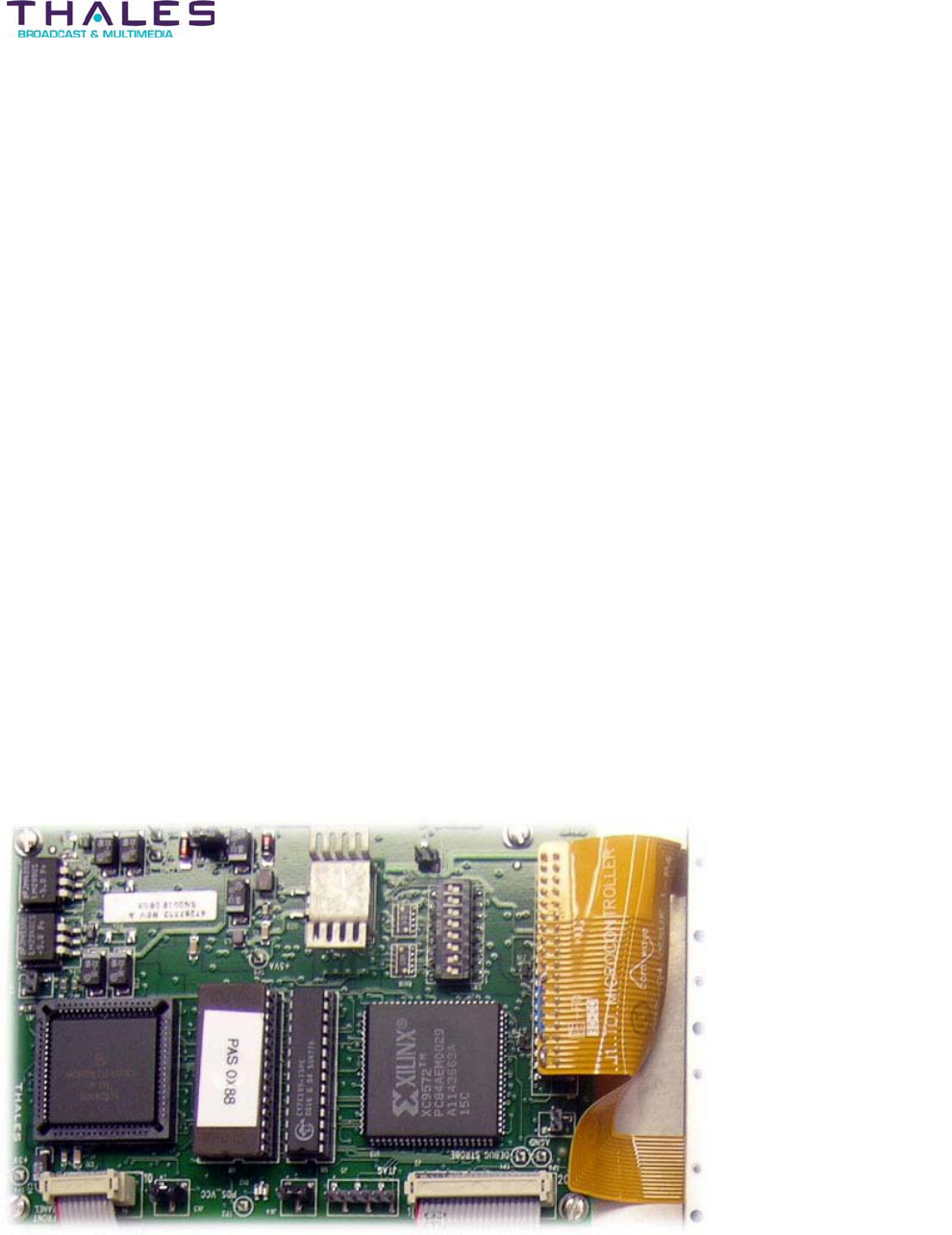
Power Amplifier Module - 111 -
®
Affinity LBD-200C-N1 Transmitter
Product Manual
serial I/O port is also available, but the RS-232 driver is disabled by default. This port is
interfaced through an RJ-11 connector on the PA Module front panel. When the ENA_RS-232
control input line is given a logic-LOW (i.e. interface cable plugged into the PA Module RJ-11
connector), the RS-232 port is enabled. At this time the RS-485 port is disabled causing a loss
of communication with the RS-485 network. The same PA Module command and response
capabilities available on the RS-485 port are provided on the RS-232 port.
A ‘watchdog’ function is provided on the control board to safeguard against loss of MCU
program control. Under normal circumstances, MCU IC input lines RESET and XIRQ will be
provided with a logic-HIGH by an on-board watchdog IC. If Jumper JK3 is in place, the CPLD
device must provide a toggle in the CPLD WDI Output line every 1.6 seconds to indicate to the
watchdog that the MCU is operating properly. The CPLD will interpret a PG3/WDI input from the
MCU, or activity on the UC_RS485_ENA control line, or activity on the RS-485 communications
lines, as indications that the MCU is operating properly, and will toggle the CPLD WDI output
line. If a toggle in the WDI line does not occur within 1.6 seconds it is assumed that MCU is no
longer executing the desired program properly. The watchdog will drive low the XORZ signal,
which will ultimately result in a reset of the MCU and a restart to the MCU program.
Two power supply inputs of approximately +10VDC are provided to the Microcontroller Board to
supply the digital and analog regulator circuits. The digital regulator circuits are fused by F1 at
the +10VDC input. A linear voltage regulator provides the +5VDC used for the digital circuitry.
The +5VDC digital circuit has a separate ground plane for the digital devices. A switching
regulator and associated components develop DC output voltages of approximately ±14.5VDC,
which is regulated by linear regulators to +12VDC and –12VDC for various digital and analog
circuits. The +5VDC analog regulator is supplied from a +10VDC separate from the digital
+10VDC input, and is fused by F2. Another linear voltage regulator develops +5VDC for the
analog circuits. The +5VDC analog circuits have a separate ground-plane for analog devices.
Microcontroller board
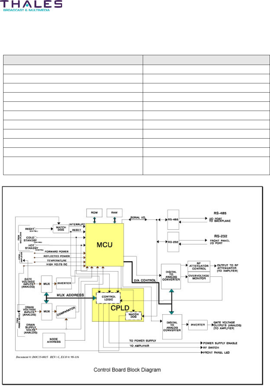
Power Amplifier Module - 112 -
®
Affinity LBD-200C-N1 Transmitter
Product Manual
Microcontroller Board Specifications:
Parameter Specification
Microcontroller type 8-bit MCU with 64K address space
Input Voltage 10VDC±0.5VDC
Input Current 400 mA typical @ 10VDC
Communication Ports RS-485 and RS-232
Program stall time before COP Watchdog Reset 1.6 seconds
Number of Analog Inputs 13
Number of Logic Inputs 7
Number of Analog Outputs 2
Number of Logic Outputs 6
Operating Temperature 0° C to 50° C
Physical Dimensions 5.125” H x 3.50” W x 0.58” D
13.0 cm H x 8.9 cm W x 1.5 cm D
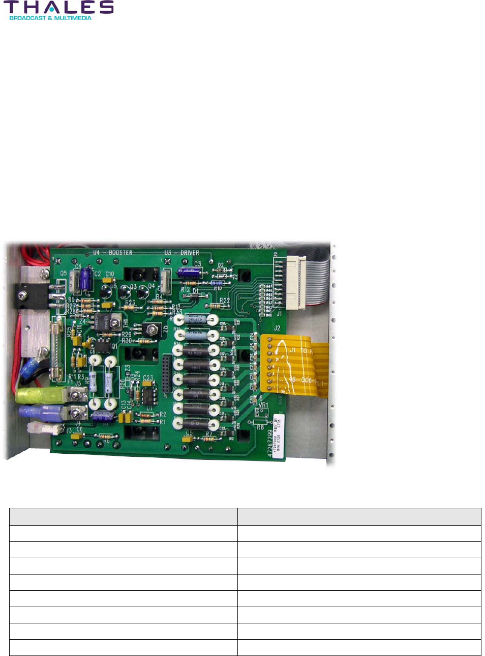
Power Amplifier Module - 113 -
®
Affinity LBD-200C-N1 Transmitter
Product Manual
Power Supply Board
The Power Supply Board consists of input and output voltage monitoring, standby switching,
over-voltage protection, and current sensing. All functions of the Power Supply Board are
interfaced with the Microcontroller Board.
The Power Supply Board switches the Front-End 48VDC Power Supply ON/OFF using a power
FET. After engaging the PA Module, the control board checks the input voltage and turns the
FET switch on. The microcontroller board will then detect the switched voltage. If the voltage
goes above or below the preset value, the microcontroller board will disable the standby switch.
The power supply distributes eight lines of power with current sensing. These lines are used for
current protection and are monitored by the microcontroller board.
Power Supply board
Power Supply Board Specifications
Parameter Specification
Primary Input Voltage 48VDC
Primary Input Voltage Range 48VDC +2.0V –1.0V
Primary Input Current 13A DC @ 32VDC +48DBMCOFDM signal
Primary Input Current Range 13A DC @ 32VDC +48DBMCOFDM signal
Output Power 70W maximum
Output Current Limit §2A above maximum @ 48 dBm COFDM signal
Efficiency §90%
Operating Temperature 0°C to 50°C
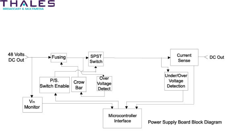
Power Amplifier Module - 114 -
®
Affinity LBD-200C-N1 Transmitter
Product Manual
PA Module Front Panel Assembly
The PA Module Front Panel Assembly houses an RS-232 COMM PORT, a bi-color
POWER/FAULT LED, and the ON/LOCKED--OFF/UNLOCKED key lock assembly. The PA
Module is also equipped with a heatsink, installation handle and thumbscrews.
The RS-232 COMM PORT 6-pin RJ11 telephone type connector is used to interface with a
serial host computer. This interface allows a host computer to control and monitor functions of
the PA Module.
The bi-color POWER/FAULT LED is used as a visual indicator for PA Module power and fault
conditions. A green LED indicates power to the PA Module. A red LED indicates a fault
condition.
The key lock assembly is used to secure the PA Module to the Chassis assembly.
In the ON/LOCKED position, the PA Module is locked into the chassis assembly and receiving
power. The PA Module cannot be removed from the chassis while in the locked position.
In the OFF/UNLOCKED position, operating power to the PA Module is disabled and the PA
Module may be removed from the chassis for service or “Hot Swap” replacement. This key lock
assembly does not affect Affinity® transmitter power.
The Heatsink is a folded-fin heat-sinking device used to dissipate heat generated by the PA
Module.
The Handle is used to insert and remove the PA Module segment.
The Thumbscrews are used to secure the PA Module segment to the Chassis.