Alcatel Canada 39T28A03A22A Alcatel 7390 LMDS Multiservice Broadband Wireless User Manual 3cc12426aaaaTQbja01
Alcatel Canada Inc Alcatel 7390 LMDS Multiservice Broadband Wireless 3cc12426aaaaTQbja01
Contents
- 1. Base Station User Manual 1 of 14
- 2. Base Station User Manual 2 of 14
- 3. Base Station User Manual 3 of 14
- 4. Base Station User Manual 4 of 14
- 5. Base Station User Manual 5 of 14
- 6. Base Station User Manual 6 of 14
- 7. Base Station User Manual 7 of 14
- 8. Base Station User Manual 8 of 14
- 9. Base Station User Manual 9 of 14
- 10. Base Station User Manual 10 of 14
- 11. Base Sation User Manual 11 of 14
- 12. Base Sation User Manual 12 of 14
- 13. Base Sation User Manual 13 of 14
- 14. Base Sation User Manual 14 of 14
Base Station User Manual 5 of 14
3CC12426AAAA TQ BJA 01 Issue 01 - April 2001 - Draft 04 111/346
128
3.4 – Base Station equipment installation
Considerations
– The rack containing the DBS sub-rack assembly and DC/DC PSUs is for indoor installation.
– The 7390BS indoor rack will be positioned according to user needs and technical constraints (e.g.,
respect of minimum distances, connections layout, RBS/DBS connection accessibility, power sup-
ply).
– The power supply is to be connected after installation of the 7390BS indoor rack, at the time of its
commissioning (cf. Chapter 5 – Commissioning the Base Station (7390BS)).
Definition of racks
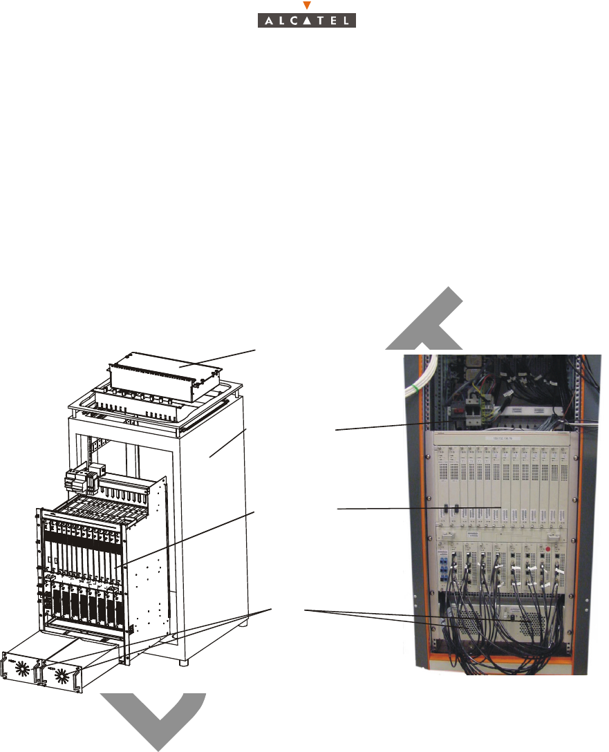
Figure 87 – Example of configuration of a 7390BS station in a standard rack
Distributors
(according to
options)
Standard 19"
rack
DBS
Sub-rack
assembly
DC/DC
power supply
units
Base station optical
112/346 Issue 01 - April 2001 - Draft 04 3CC12426AAAA TQ BJA 01
128
3.4.1 – Mechanical installation
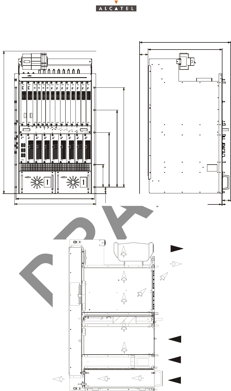
Figure 88 – Chassis dimensions and clearances (dimensions in mm)
– Respect the requested clearances for the wiring, in order to avoid damage to the connectors (mar-
ked with an*).
Figure 89 – Ventilation of the DBS chassis (cross-section)
19u*
844.55
38.1 133.3
323.9
457.2
590.5
465
19”482.6
440
540*
50*
2,5
50*
Ambient air
do not obstruct inlet
Heated air
do not obstruct outlet
3CC12426AAAA TQ BJA 01 Issue 01 - April 2001 - Draft 04 113/346
128
– The installation of rack (optional) and chassis must enable the ventilation shown Figure 89 – Ven-
tilation of the DBS chassis (cross-section). Do not obstruct the air inlets and outlets.
Stages
1. Choose the location where the equipment is to be assembled and unpack the standard rack. If its
top cover is fitted, remove it (quarter-turn screw).
Note: place the rack in such a way that the cable connections are accessible before the rack is installed
definitively.
2. Unpack the DBS chassis assembly and install it inside the rack. Fix and screw into place.
3. Unpack the DC/DC PSUs; install and plug them in the DBS chassis.
4. Carry out the electrical connection, cf. § 3.4.2 – Electrical connection.
5. Carry out the client terminal connections, cf. § 3.4.3 – Customer access connections (circuits
interfaces) and 3.4.4 – Client access connections (ATM network interface).
6. Connect the X-Pol RBS/DBS connection cable(s).
3.4.2 – Electrical connection
Considerations
– The DBS chassis is supplied from the rated DC voltage of 48 V (minimum 35 V, maximum 60 V).
– The cable connecting the external DC power source to the DBS sub-rack will have a minimum
cross-section of 3x10 mm2 and a maximum length of 20 meters.
– The rack must be grounded to the general grounding system. For this, the rack mechanism will be
connected by a cable with a minimum cross-section of 16 mm2 , attached using a 6 mm bolt.
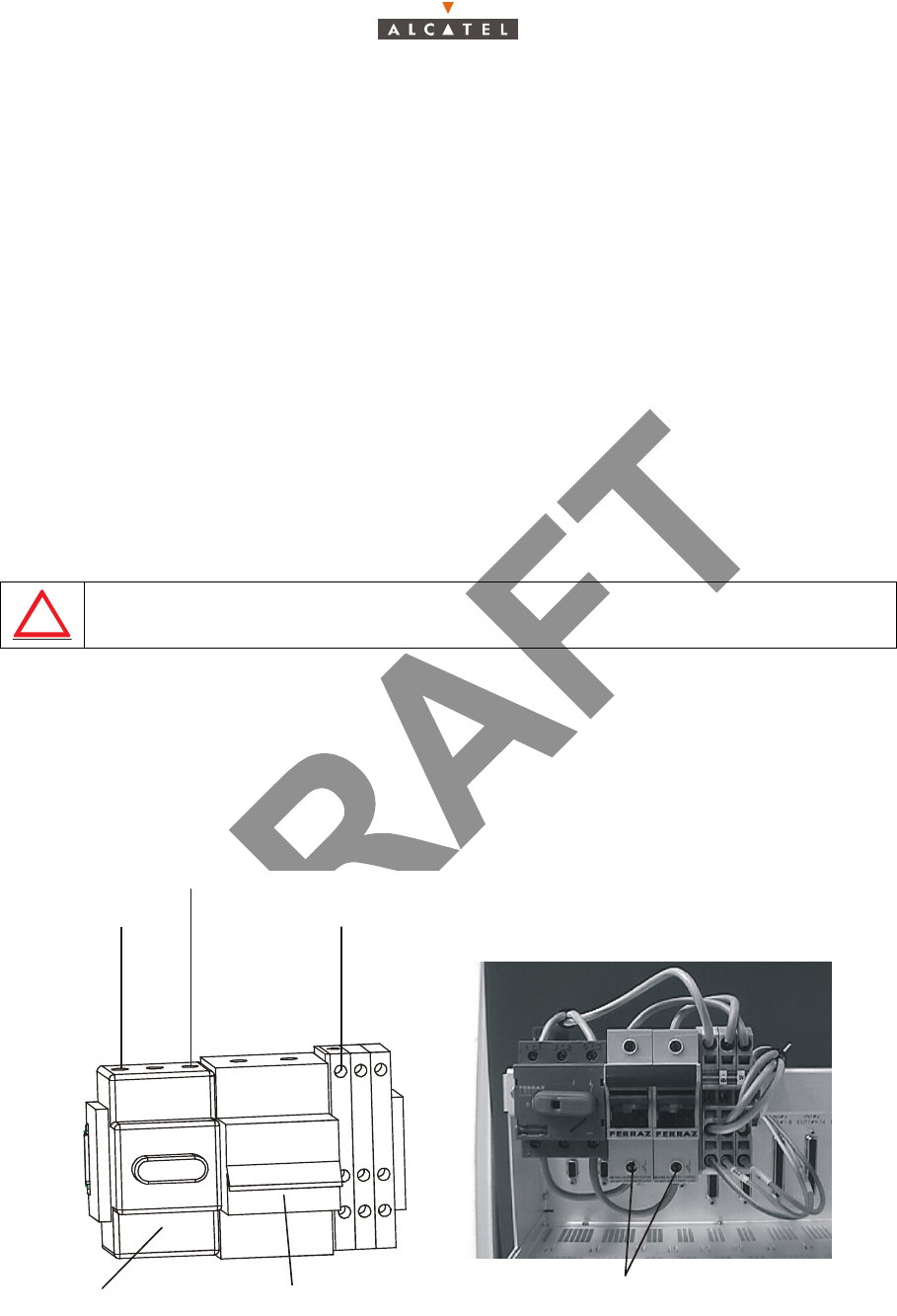
– For the power supply block diagram, refer to Figure 90 – DBS chassis power supply:
Figure 90 – DBS chassis power supply
WHEN MAKING THE POWER CONNECTIONS, TURN OFF ALL DBS
CHASSIS EXTERNAL POWER SOURCES
0V/+48V
–48V/0V
Grounding
Fuse holder
ON – OFF switch Fuse cartridge GRC
14x51 40 Am
p
.
114/346 Issue 01 - April 2001 - Draft 04 3CC12426AAAA TQ BJA 01
128
Note: The user can connect +48 V or -48 V to ground.
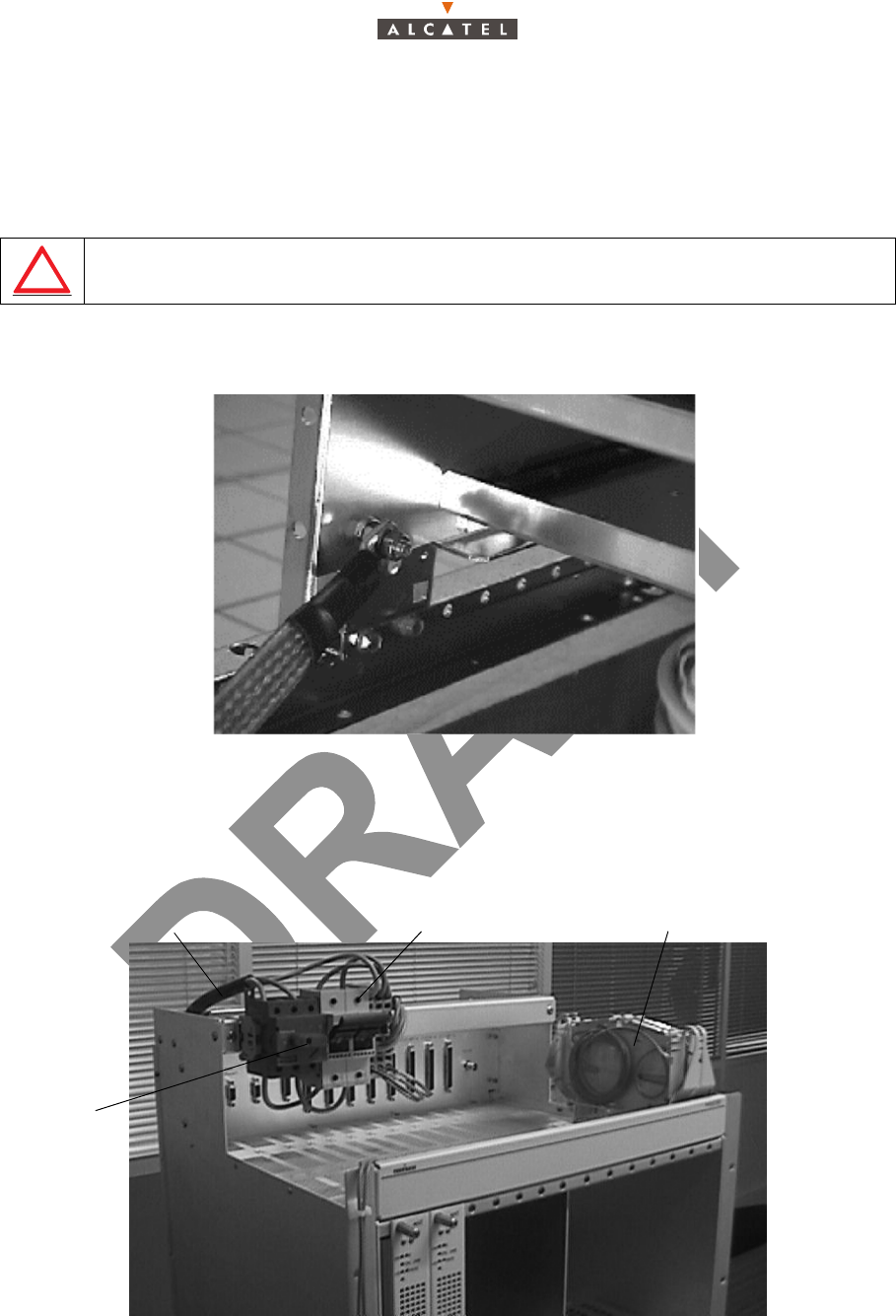
Stages (Figure 92 – DBS sub-rack power connection)
1. Connect the switch at the top of the DBS sub-rack to the external DC power source. You are
recommended to pass the power supply cable via the top of the rack.
2. Ground the DBS sub-rack.
Note: a ground strip is fixed to the backplane and ensures its grounding. The rack and subrack ground
are screwed together, thus no special grounding is required for the rack.
Figure 91 – DBS sub-rack ground connection
Earthing must be done very carefully in order to assure good operation of the DBS.
3. Make sure that the fuses are inserted in the fuse-holder. Before changing fuse, make sure that the
switch is set to OFF.
Figure 92 – DBS sub-rack power connection
ATTENTION: DO NOT CONNECT THE GROUNDING CABLE TO THE SWITCH
BUT TO THE YELLOW/GREEN TERMINAL BLOCK
Fuse-holderPower supply cables
ON - OFF
Switch
Winding cassette for fiber optic
cables
3CC12426AAAA TQ BJA 01 Issue 01 - April 2001 - Draft 04 115/346
128
3.4.3 – Customer access connections (circuits interfaces)
Considerations
This connection involves the use of:
– either direct connectors TNT1 to TNT4, (corresponding to TNT board plug into the chassis) at
the top of the DBS sub-rack, if no distribution frames (cf. § 3.4.3.1 – Direct connections to the con-
nectors of the top panel of the DBS chassis.);
– or the optional distribution frames at the top of the DBS sub-rack in the standard rack (coaxial
cables for the 75 ohm links, balanced pair cables for the 120 ohm links cf. § 3.4.3.2 – Connections
to 75 ohm coaxial distributors and § 3.4.3.3 – Connections to 120 ohm distributors).
Note: the provided equipment is already connected and parts of the installation kit.
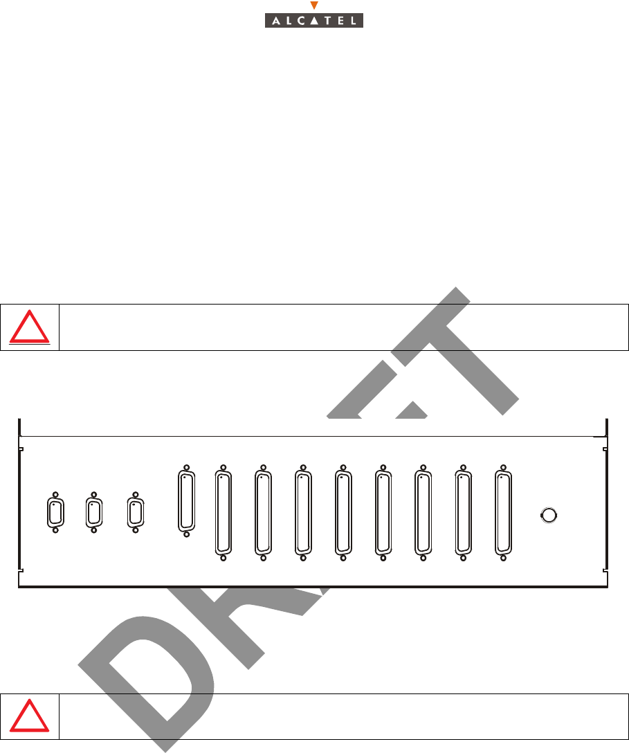
3.4.3.1 – Direct connections to the connectors of the top panel of the DBS chassis.
Note: All connectors are female connectors.
Figure 93 – Top panel DBS connections: connectors location
ALL CUSTOMER ACCESS CABLES MUST BE SHIELDED TYPE
DO NOT REMOVE THE COVER ON CONNECTOR TEST J113
TEST#1
NMS
(10baseT)
SYNCHRO
2,048Mz
ALARMS
I/O TNT#1
E1/T1#1–8
TNT#1
E1/T1#9–16 TNT#2
E1/T1#1–8
TNT#2
E1/T1#9–16 TNT#3
E1/T1#1–8
TNT#3
E1/T1#9–16 TNT#4
E1/T1#1–8
TNT#4
E1/T1#9–16
TEST#2
J101 J102 J104
J103
J105 J106 J107 J108 J109 J110 J111 J112
J113
116/346 Issue 01 - April 2001 - Draft 04 3CC12426AAAA TQ BJA 01
128
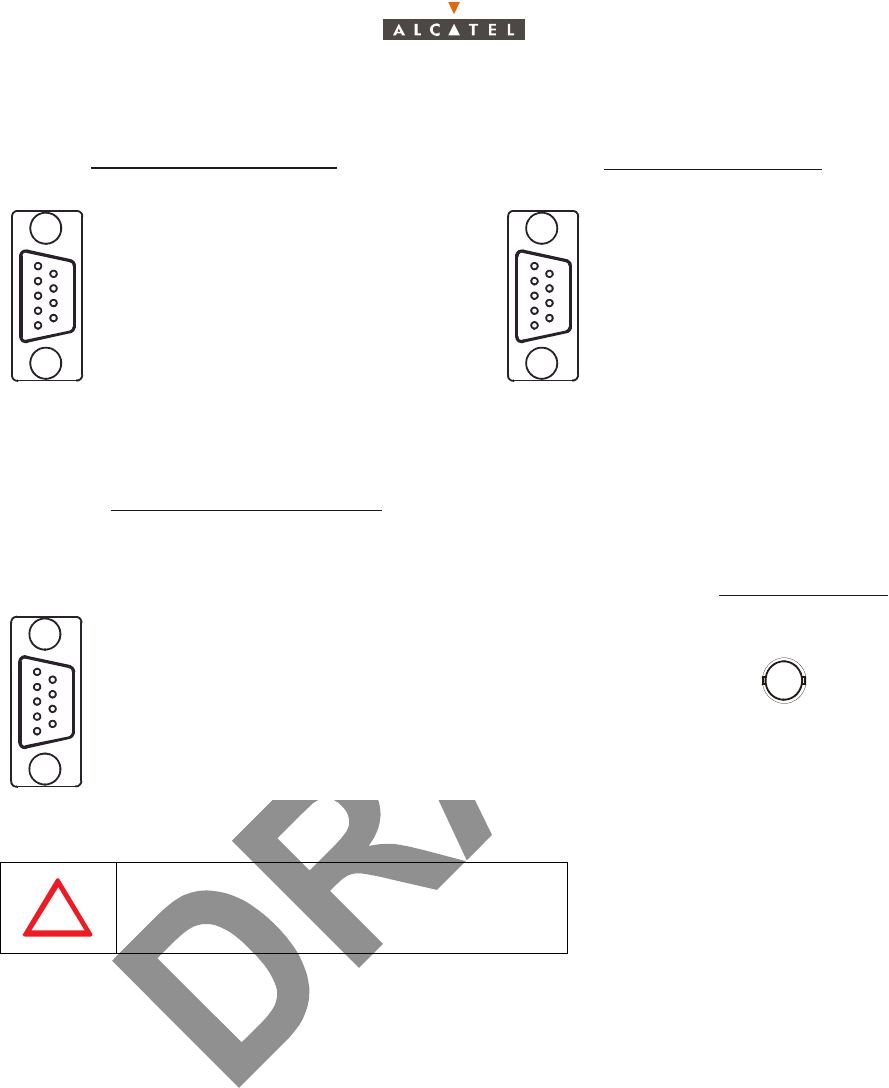
Figure 94 – DBS connections, assignment of access points (1)
Do not connect pins 01 and 06
(clock output: 75 ohms load, 06 connected to
ground)
Pin 01: not connected
Pin 02: ground
Pin 03: ground
Pin 05: not connected
Pin 07: 10BT_RxD_P
Pin 08: 10BT_TxD_M
Pin 04: ground
Pin 06: 10BT_RxD_M
CONNECTOR NMS J102
Pin 01: SDA_Fdp
Pin 02: ground
Pin 03: ground
Pin 07: ground
Pin 08: PC_RS232_Tx_1
Pin 04: PC_RS232_Rx_1
Pin 06: SCL_Fdp
CONNECTOR TEST#1 J101
Pin 05: PC_RS232_Rx_0
Pin 09: PC_RS232_Tx_0 Pin 09: 10BT_TxD_P
51
69
51
69
Pin 01: Clk_2M_Out_P
Pin 02: ground
Pin 03: ground
Pin 05: Clk_2M_In_M
Pin 07: ground
Pin 08: ground
Pin 04: ground
Pin 06: Clk_2M_Out_M
Pin 09: Clk_2M_In_P
CONNECTOR SYNCHRO J103
51
69
(do not connect)
(do not connect)
TEST#2
J113
CONNECTOR J113
DO NOT CONNECT
Clock signals have no polarity
––
> P and M not significant
(clock input)
(clock input)
3CC12426AAAA TQ BJA 01 Issue 01 - April 2001 - Draft 04 117/346
128
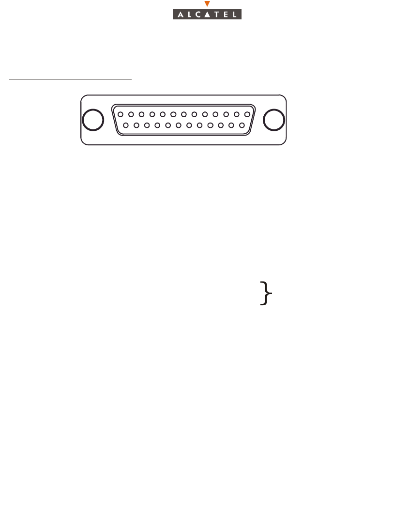
CONNECTOR ALARM J104
Pin 01: I_AL_0 Remote signaling input 1
Pin 04: I_AL_6 Remote signaling input 7
Pin 05: ground
Pin 06: ground
Pin 07: ATT_B ATTENDED alarm relay idle
Pin 08: NURG_B NON–URGENT alarm relay idle
Pin 09: URG_B URGENT alarm relay idle
Pin 10: CMD_4_B Remote control # 4 idle
Pin 11: CMD_3_B Remote control # 3 idle
Pin 12: CMD_2_B Remote control # 2 idle
Pin 13: CMD_1_B Remote control # 1 idle
Pin 14: I_AL_1 Remote signaling input 2
Pin 15: I_AL_3 Remote signaling input 4
Pin 16: I_AL_5 Remote signaling input 6
Pin 17: I_AL_7 Remote signaling input 8
Pin 18: Ground
Pin 19: ATT_A ATTENDED alarm common relay
Pin 20: NURG_A NON–URGENT alarm common relay
Pin 21: URG_A URGENT alarm common relay
Pin 22: CMD_4_A Common remote control # 4
Pin 23: CMD_3_A Common remote control # 3
Pin 24: CMD_2_A Common remote control # 2
Pin 25: CMD
_
1
_
A Common remote control # 1
Pin 02: I_AL_2 Remote signaling input 3
Pin 03: I_AL_4 Remote signaling input 5
1
13
14
25
ALARMS
Red “UG” and “NUG” LEDs
(not managed in NR 2.2)
Red “UG” and “NUG” LED
s
(not managed in NR 2.2)
}

118/346 Issue 01 - April 2001 - Draft 04 3CC12426AAAA TQ BJA 01
128
Figure 95 – DBS connections, assignment of access points (2)
Pin 01: ground
Pin 04: Input_3_P_1
Pin 05: Input_4_P_1
Pin 06: Input_5_P_1
Pin 07: Input_6_P_1
Pin 08: Input_7_P_1
Pin 09: Input_8_P_1
Pin 10: ground
Pin 11: ground
Pin 12: Output_1_P_1
Pin 13: Output_2_P_1
Pin 14: Output_3_P_1
Pin 15: Output_4_P_1
Pin 16: Output_5_P_1
Pin 17: Output_6_P_1
Pin 18: Output_7_P_1
Pin 19: Output_8_P_1
Pin 20: ground
Pin 21: Input_1_M_1
Pin 22: Input_2_M_1
Pin 23: Input_3_M_1
Pin 24: Input_4_M_1
Pin 25: Input_5_M_1
Pin 26: Input_6_M_1
Pin 27: Input_7_M_1
Pin 28: Input_8_M_1
Pin 29: ground
Pin 30: Output_1_M_1
Pin 31: Output_2_M_1
Pin 32: Output_3_M_1
Pin 33: Output_4_M_1
Pin 34: Output_5_M_1
Pin 35: Output_6_M_1
Pin 36: Output_7_M_1
Pin 37: Output_8_M_1
Pin 02: Input_1_P_1
Pin 03: Input_2_P_1
ground
Input_11_P_2
Input_12_P_2
Input_13_P_2
Input_14_P_2
Input_15_P_2
Input_16_P_2
ground
ground
Output_9_P_2
Output_10_P_2
Output_11_P_2
Output_12_P_2
Output_13_P_2
Output_14_P_2
Output_15_P_2
Output_16_P_2
ground
Input_9_M_2
Input_10_M_2
Input_11_M_2
Input_12_M_2
Input_13_M_2
input_14_M_2
Input_15_M_2
Input_16_M_2
ground
Output_9_M_2
Output_10_M_2
Output_11_M_2
Output_12_M_2
Output_13_M_2
Output_14_M_2
Output_15_M_2
Output_16_M_2
Input_9_P_2
Input_10_P_2
ground
Input_3_P_3
Input_4_P_3
Input_5_P_3
Input_6_P_3
Input_7_P_3
Input_8_P_3
ground
ground
Output_1_P_3
Output_2_P_3
Output_3_P_3
Output_4_P_3
Output_5_P_3
Output_6_P_3
Output_7_P_3
Output_8_P_3
ground
Input_1_M_3
Input_2_M_3
Input_3_M_3
Input_4_M_3
Input_5_M_3
input_6_M_3
Input_7_M_3
Input_8_M_3
ground
Output_1_M_3
Output_2_M_3
Output_3_M_3
Output_4_M_3
Output_5_M_3
Output_6_M_3
Output_7_M_3
Output_8_M_3
Input_1_P_3
Input_2_P_3
ground
Input_11_P_4
Input_12_P_4
Input_13_P_4
Input_14_P_4
Input_15_P_4
Input_16_P_4
ground
ground
Output_9_P_4
Output_10_P_4
Output_11_P_4
Output_12_P_4
Output_13_P_4
Output_14_P_4
Output_15_P_4
Output_16_P_4
ground
Input_9_M_4
Input_10_M_4
Input_11_M_4
Input_12_M_4
Input_13_M_4
input_14_M_4
Input_15_M_4
Input_16_M_4
ground
Output_9_M_4
Output_10_M_
4
Output_11_M_
4
Output_12_M_
4
Output_13_M_
4
Output_14_M_
4
Output_15_M_
4
Output_16_M_
4
Input_9_P_4
Input_10_P_4
TNT#1
E1/T1#1–8
J105
TNT#1
E1/T1#9–16
J106
TNT#2
E1/T1#1–8
J107
TNT#2
E1/T1#9–16
J108
37
19 1
20
P = +
/
M = –

3CC12426AAAA TQ BJA 01 Issue 01 - April 2001 - Draft 04 119/346
128
Figure 96 – DBS connections, assignment of access points (3)
37
19 1
20
ground
Input_11_P_6
Input_12_P_6
Input_13_P_6
Input_14_P_6
Input_15_P_6
Input_16_P_6
ground
ground
Output_9_P_6
Output_10_P_6
Output_11_P_6
Output_12_P_6
Output_13_P_6
Output_14_P_6
Output_15_P_6
Output_16_P_6
ground
Input_9_M_6
Input_10_M_6
Input_11_M_6
Input_12_M_6
Input_13_M_6
input_14_M_6
Input_15_M_6
Input_16_M_6
ground
Output_9_M_6
Output_10_M_6
Output_11_M_6
Output_12_M_6
Output_13_M_6
Output_14_M_6
Output_15_M_6
Output_16_M_6
Input_9_P_6
Input_10_P_6
ground
Input_3_P_7
Input_4_P_7
Input_5_P_7
Input_6_P_7
Input_7_P_7
Input_8_P_7
ground
ground
Output_1_P_7
Output_2_P_7
Output_3_P_7
Output_4_P_7
Output_5_P_7
Output_6_P_7
Output_7_P_7
Output_8_P_7
ground
Input_1_M_7
Input_2_M_7
Input_3_M_7
Input_4_M_7
Input_5_M_7
input_6_M_7
Input_7_M_7
Input_8_M_7
ground
Output_1_M_7
Output_2_M_7
Output_3_M_7
Output_4_M_7
Output_5_M_7
Output_6_M_7
Output_7_M_7
Output_8_M_7
Input_1_P_7
Input_2_P_7
ground
Input_11_P_8
Input_12_P_8
Input_13_P_8
Input_14_P_8
Input_15_P_8
Input_16_P_8
ground
ground
Output_9_P_8
Output_10_P_8
Output_11_P_8
Output_12_P_8
Output_13_P_8
Output_14_P_8
Output_15_P_8
Output_16_P_8
ground
Input_9_M_8
Input_10_M_8
Input_11_M_8
Input_12_M_8
Input_13_M_8
input_14_M_8
Input_15_M_8
Input_16_M_8
ground
Output_9_M_8
Output_10_M_8
Output_11_M_8
Output_12_M_8
Output_13_M_8
Output_14_M_8
Output_15_M_8
Output_16_M_8
Input_9_P_8
Input_10_P_8
TNT#3
E1/T1#1–8
J109
TNT#3
E1/T1#9–16
J110
TNT#4
E1/T1#1–8
J111
TNT#4
E1/T1#9–16
J112
Pin 01: ground
Pin 04: Input_3_P_5
Pin 05: Input_4_P_5
Pin 06: Input_5_P_5
Pin 07: Input_6_P_5
Pin 08: Input_7_P_5
Pin 09: Input_8_P_5
Pin 10: ground
Pin 11: ground
Pin 12: Output_1_P_5
Pin 13: Output_2_P_5
Pin 14: Output_3_P_5
Pin 15: Output_4_P_5
Pin 16: Output_5_P_5
Pin 17: Output_6_P_5
Pin 18: Output_7_P_5
Pin 19: Output_8_P_5
Pin 20: ground
Pin 21: Input_1_M_5
Pin 22: Input_2_M_5
Pin 23: Input_3_M_5
Pin 24: Input_4_M_5
Pin 25: Input_5_M_5
Pin 26: Input_6_M_5
Pin 27: Input_7_M_5
Pin 28: Input_8_M_5
Pin 29: ground
Pin 30: Output_1_M_5
Pin 31: Output_2_M_5
Pin 32: Output_3_M_5
Pin 33: Output_4_M_5
Pin 34: Output_5_M_5
Pin 35: Output_6_M_5
Pin 36: Output_7_M_5
Pin 02: Input_1_P_5
Pin 03: Input_2_P_5
Pin 37: Output_8_M_5
P = +
/
M = –
120/346 Issue 01 - April 2001 - Draft 04 3CC12426AAAA TQ BJA 01
128
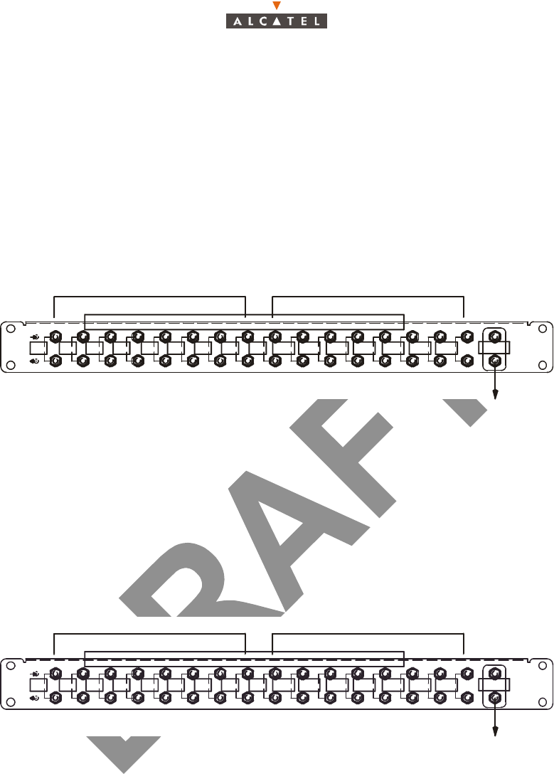
3.4.3.2 – Connections to 75 ohm coaxial distributors
Connections are made beneath the roof of the standard rack or on the front panel for a different type of
rack.
Optional cables and distributors are in the installation set.
1.6 / 5.6, 75 ohm distributor for16 E1 / T1, ref: 3CC08061AAxx.
– One distributor per TNT board.
– TNT connectors (J105 to J112) connected to the top panel of the DBS subrack with (n)
3CC11236AAxx cable(s).
Figure 97 – 1.6/5.6, 75 ohm distributor
75 ohm BNC distributor for16 E1 / T1 ref.: 3CC08061ABxx.
– One distributor per TNT board.
– TNT connectors (J105 to J112) connected to the top panel of the DBS subrack with (n)
3CC11237AAxx cable(s).
Figure 98 – BNC 75 ohm distributor
1 2 3 4 5 6 7 8 9 10 11 12 13 14 15 16
A
UX
E1/T1 1 – 8 E1/T1 9 – 16
not connected
1 2 3 4 5 6 7 8 9 10 11 12 13 14 15 16
A
UX
E1/T1 1 – 8 E1/T1 9 – 16
not connected