Nokia Solutions and Networks T5GX1 UBS CDMA XMI Transceiver at 800 MHz User Manual Exhibit 122b
Nokia Solutions and Networks UBS CDMA XMI Transceiver at 800 MHz Exhibit 122b
Contents
Exhibit 122b
RX Splitter Equipment Identication Chapter 1: Ov erview
RX Splitter Equipment Identication■■■■■■■■■■■■■■■■■■■■■■■■■■■■■■■■■■■■■■■■■■■■■■■■■■■■■■■■■■■■■■
■
■
RX Splitter I/O Panel
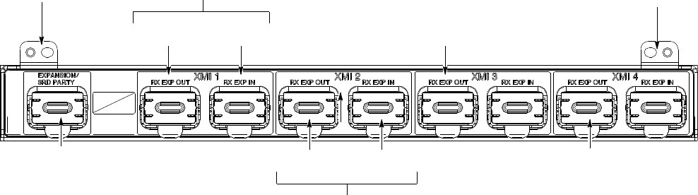
Figure 1 -14 shows the wide band (800 MHz -to -2.1 GHz) RX splitter I/O panel.
Figure 1 -14 RX splitter front panel detail
WIDE BAND
RX SPLITTER
ti-cdma-06110.eps
Mounting
Tab Mounting
Tab
EXP OUT
(RX MAIN)
EXPANSION/
3RD PARTY
(Signal source via
splitter: RX MAIN is XMI 1
and RX DIV is XMI 2.)
NOTES:
1. All RX splitter connectors are ganged mini-coaxial.
2. RX EXP IN signal flow direction is from XMI.
RX EXP OUT signal flow direction is to XMI.
3. Used in both 1.9 GHz and 800 MHz multi-XMI
applications.
EXP IN
(RX DIV ) Future - XMI 3 EXP OUT
(RX MAIN & DIV)
Future - XMI 4 EXP OUT
(RX MAIN & DIV)
XMI 1
EXP IN
(RX MAIN)
EXP OUT
(RX DIV )
XMI 2
WIDE BAND SPLITTER
1 -44 68P09283A64 -3
FOA SEP 2007
1X UBS Macro B T S FRU P ower Supply Module (PSM) Shelf Equipment Identication
Power Supply Module (PSM) Shelf Equipment
Identication
■■■■■■■■■■■■■■■■■■■■■■■■■■■■■■■■■■■■■■■■■■■■■■■■■■■■■■■■■■■■■■
■
■
PSM I/O Panels
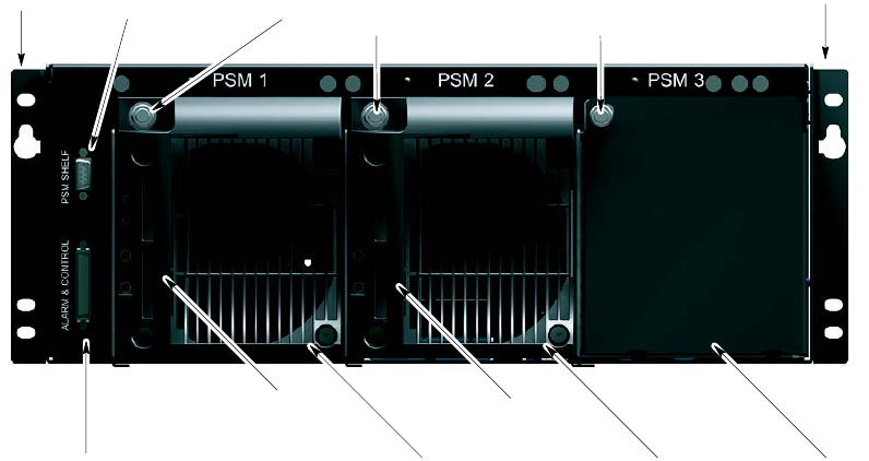
Figure 1 -15 shows I/O connectors and PSM slot locations on the front panel of the UBS Macro
BTS –48 V DC and 220 V AC PSM shelves. This figure also briefly describes connector usage.
A PSM will be used in PSM 3 slot when more +27 V DC output power is needed to support
additional equipment.
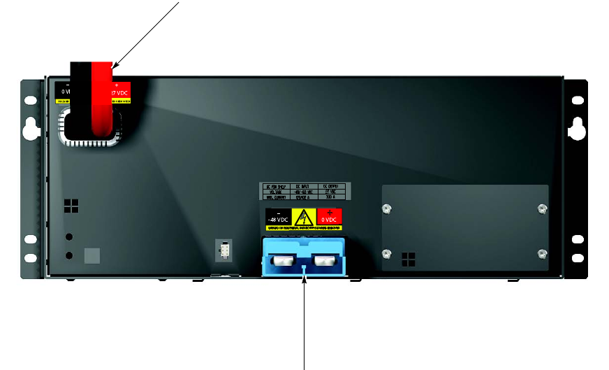
Figure 1 -16 shows I/O cable and connector locations on the rear panel of the UBS Macro BTS
—48 V DC PSM shelf . This figure also briefly describes cable and connector usage.
Figure 1 -17 shows I/O cable, connector and terminal locations on the rear panel of the UBS
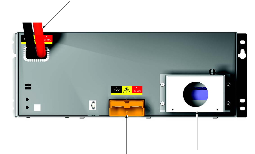
Macro BTS 220 V AC PSM shelf . This figure also briefly describes cable and connector usage.
68P09283A64 -3 1 -45
FOA SEP 2007
P ower Supply Module (PSM) Shelf Equipment Identication Chapter 1: Ov erview
Figure 1 -15 –48 V DC and 220 V AC PSM shelv es front panel detail
ti-cdma-05915.eps
Rack
Mounting
Flange
PSM SHELF
(9-pin sub-D Connector)
NOTE 1
AC or -48 V DC PSM Shelf
(front view) Rack
Mounting
Flange
ALARM & CONTROL
(50-pin Connector)
NOTE 2 Connects to ALARM
& CONTROL Connector on SSI
PSM 1 PSM 2 PSM 3
Empty Slot with
Blank Filler Panel
NOTES:
1. The PSM SHELF connector is only used when the UBS Macro frame is
equipped with two optional AC or -48 V DC PSM shelves. In this case, the
PSM SHELF connectors on the two PSM shelves are interconnected.
2. The ALARM & CONTROL connector connects to ALARM & CONTROL
connector on the SSI. If the UBS Macro frame is equipped with two optional
AC or -48 V DC PSM shelves, only one shelf has this connector cabled.
PSM Captive Retaining
Thumbscrew
Filler Panel Captive
Retaining Thumbscrew
PSM
Handle PSM
Handle
1 -46 68P09283A64 -3
FOA SEP 2007
1X UBS Macro B T S FRU P ower Supply Module (PSM) Shelf Equipment Identication
Figure 1 -16 –48 V DC PSM shelf rear panel detail
_
-48 VDC 0 VD
C
_
0 VDC
+
27 V
DC
HAZARD OF ELECTRICAL SHOCK WITH COVERS REMOVED
ti-cdma-05916.eps
+27 V DC Output
Power Cable
(shown cut away)
To PDU
-48 VDC Input
Power Connector
(Blue)
68P09283A64 -3 1 -47
FOA SEP 2007
P ower Supply Module (PSM) Shelf Equipment Identication Chapter 1: Ov erview
Figure 1 -17 220 V AC PSM shelf rear panel detail
ti-cdma-05917.eps
+27 V DC Output
Power Connector
(Orange) Note 2
AC Input
Terminal Block
Protective Cover
NOTES:
1. Equipment shown is typical. The actual equipment appearance may vary slightly.
2. The +27 V DC Output connector may be connected to back-up batteries, but usage is optional.
+27 V DC Output
Power Cable
(shown cut away)
To PDU
_
0 VDC
+
27 VDC
HAZARD OF ELECTRICAL SHOCK WITH COVERS REMOVED
_
0 VDC
+
27 VDC
HAZARD OF ELECTRICAL SHOCK WITH COVERS REMOVED
1 -48 68P09283A64 -3
FOA SEP 2007

1X UBS Macro B T S FRU Optional RGPS Head Equipment Identication
Optional RGPS Head Equipment Identication■■■■■■■■■■■■■■■■■■■■■■■■■■■■■■■■■■■■■■■■■■■■■■■■■■■■■■■■■■■■■■
■
■
The information in this section of the manual will aid in identifying the optional RGPS head
equipment.
Any of the following RGPS heads may be used with the UBS Macro BTS:
•STLN6594 (Motorola part number)
•0186012H04 (Motorola part number)
The STLN6594 RGPS head is recommended and ships with the UBS Macro BTS when the
optional RGPS head is ordered.
The 0186012H04 RGPS head is an alternate and may be in use in the field as a replacement
spare.
Motorola recommends that the STLN6594 RGPS head be used as a replacement spare.
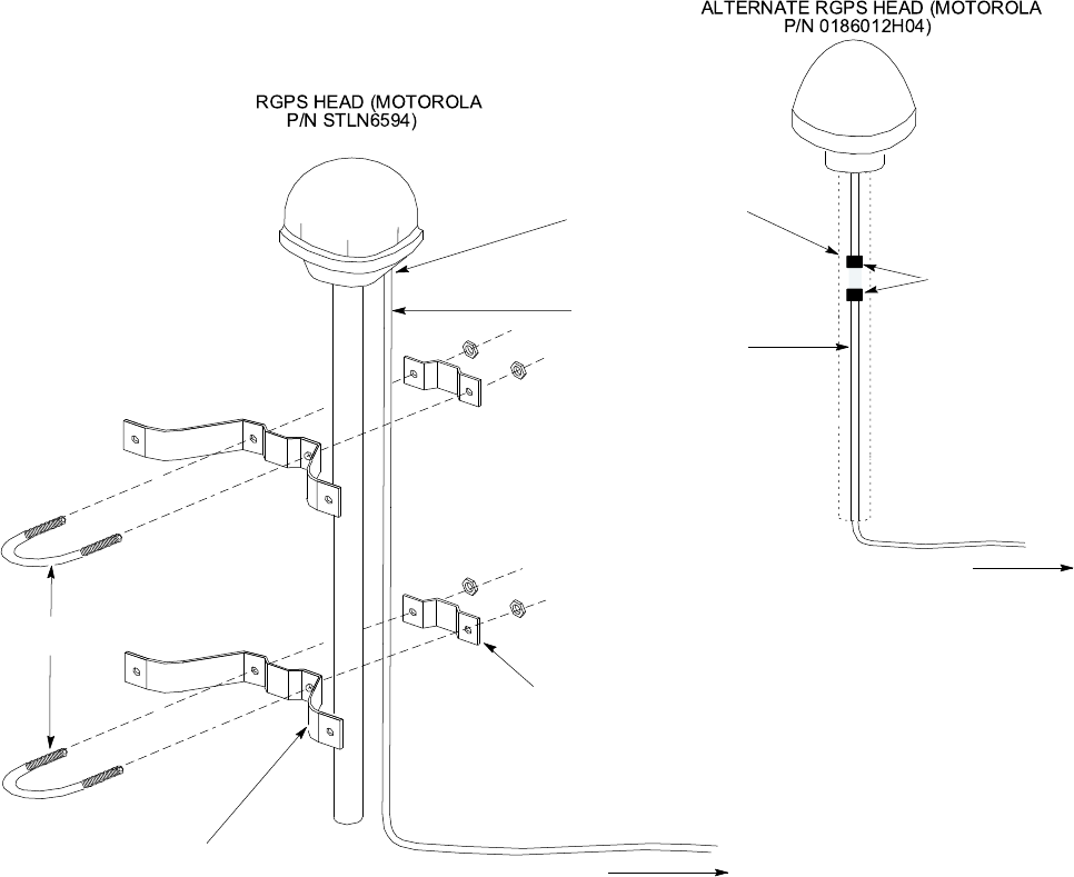
RGPS Head Mounting Method
The RGPS head is mounted outdoors on a pole. The pole is typically mounted to a wall. See
Figure 1 -18 for details.
68P09283A64 -3 1 -49
FOA SEP 2007
Optional RGPS Head Equipment Identication Chapter 1: Ov erview
Figure 1 -18 RGPS Head Mounting Details
Based on: ti-cdma-05740.eps
WALL MOUNTING
BRACKETS (2)
CLAMP BRACKETS (2)
U-BOLTS
CABLE TO LIGHTNING
ARRESTOR
RGPS HEAD WITH
12 PIN MALE
CONNECTOR
MATING
CONNECTORS
RGPS INTERFACE
CABLE WITH 12 PIN
FEMALE CONNECTOR
ON ONE END AND
UNTERMINATED WIRE
ON OTHER END
CABLE TO LIGHTNING
ARRESTOR
ALTERNATE RGPS HEAD (MOTOR OLA
P/N 0186012H04)
RGPS H EAD (MOTORO LA
P/N STLN6594)
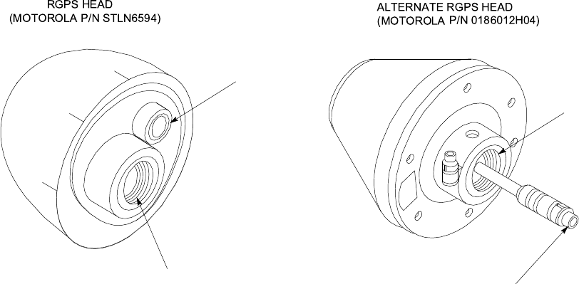
RGPS Head Details
The STLN6594 and 0186012H04 RGPS heads have similar connectors and threaded pole
mount adapters, but the implementation and location of these items varies between the two
heads (see Figure 1 -19 ).
1 -50 68P09283A64 -3
FOA SEP 2007
1X UBS Macro B T S FRU Optional RGPS Head Equipment Identication
Figure 1 -19 RGPS Head Equipment
ti-cdma-05702.eps
THREADED MOUNT
ADAPTER
THREADED MOUNT
ADAPTER 12-PIN DEUTSCH
TYPE MMP CONNECTOR
12-PIN DEUTSCH
TYPE MMP CONNECTOR
ALTERNATE RGPS HEAD
(MOTOROLA P/N 0186012H04)
RGPS HEAD
(MOTOROLA P/N STLN 6594)
68P09283A64 -3 1 -51
SEP 2007 FOA
Optional RGPS Head Equipment Identication Chapter 1: Ov erview
1 -52 68P09283A64 -3
FOA SEP 2007

C h a p t e r
2
Reference Procedures Performed At BTS Site■■■■■■■■■■■■■■■■■■■■■■■■■■■■■■■■■■■■■■■■■■■■■■■■■■■■■■■■■■■■■■
■
■
■
■
68P09283A64 -3 2 -1
SEP 2007 FOA
R eference Procedures P erformed at B T S Site Chapter 2: R eference Procedures P erformed A t B T S Site
Reference Procedures Performed at BTS Site■■■■■■■■■■■■■■■■■■■■■■■■■■■■■■■■■■■■■■■■■■■■■■■■■■■■■■■■■■■■■■
■
■
Introduction
The procedures in this chapter are referenced during various FRU replacement procedures
and are performed by the technician at the BTS site. These reference procedures include the
following:
•Frame power down and power -up sequence
2 -2 68P09283A64 -3
FOA SEP 2007

1X UBS Macro B T S FRU Fr ame P ower Down & P ower -Up Procedures
Frame Power Down & Power -Up Procedures■■■■■■■■■■■■■■■■■■■■■■■■■■■■■■■■■■■■■■■■■■■■■■■■■■■■■■■■■■■■■■
■
■
Powering Down the Frame
Prior to powering down the frame, perform the steps in Procedure 3 -2 Shutdown site
signaling functions procedure for a packet BTS on page 3 - 5 .
P ower down the frame by performing the steps in Procedure 2 -1 .
Procedure 2 -1 P owering Down the Fr ame
A T THE BTS SITE
1
Set all PDU DC circuit breakers to OFF (pulled out) in the following sequence (see
Figure 1-12 PDU front panel detail on page 1- 42 ):
•XMI 1 through XMI 4 (up to four breakers)
•DMI 1 through DMI 5 (up to five breakers)
•S SI 1 through S SI 2 (up to two breakers)
•ACC 1 through ACC 2 (up to two accessory breakers)
2
If the BTS site is equipped with backup batteries, set all battery circuit breakers to the
OFF position.
3
F or a +27 V DC powered UBS Macro frame, set the facility circuit breaker
controlling external +27 V DC power to the frame to the OFF position.
F or a — 48 V DC powered UBS Macro frame, set the facility circuit breaker
controlling external 48 V DC power to the PSM to the OFF position.
F or an AC powered UBS Macro frame, set the facility circuit breaker controlling
external AC power to the PSM to the OFF position.
Power -up the Frame
P ower -up the frame by performing the steps in Procedure 2 -2 .
68P09283A64 -3 2 -3
FOA SEP 2007

Fr ame P ower Down & P ower -Up Procedures Chapter 2: R eference Procedures P erformed A t B T S Site
Procedure 2 -2 P owering Up the Fr ame
A T THE BTS SITE
1
F or a +27 V DC powered UBS Macro frame, set the facility circuit breaker
controlling external +27 V DC power to the frame to the ON position.
F or a — 48 V DC powered UBS Macro frame, set the facility circuit breaker
controlling external 48 V DC power to the PSM to the ON position.
F or an AC powered UBS Macro frame, set the facility circuit breaker controlling
external AC power to the PSM to the ON position.
2
On the PDU , set the S SI circuit breakers to the ON position.
3
Check that the ST A TUS LED on the front panel of the each S SI is lighted.
4
F or BTSs with more than one DMI, during troubleshooting or for forcing one
DMI to synchronize code and data with the other DMI, it may be desired to
bring up a particular DMI as the site master . In this case, power up the DMI
that should be site master first, wait 1 minute, and then power up the other
DMI that should be non-site master . The non-site master DMI will synchronize
its code load and base file with the site master DMI.
On the PDU , set the DMI circuit breakers for all of the equipped DMIs to the ON position.
Circuit breakers for any DMIs that are not equipped, should be set to the OFF position.
5
Check that the ST LED on the front panel of each DMI is lighted.
6
Confirm that the DMI fans are on and operating by listening for fan motor hum and
feeling that air is being exhausted from the rear of the DMIs.
7
On the PDU , set the XMI circuit breakers to the ON position. There may be up to four
XMI circuit breakers; XMI 1 through XMI 4. Circuit breakers for any XMIs that are not
equipped, should be set to the OFF position.
8
Check that the ST/ALM LED on the front panel of each the XMI is lighted. Confirm that
the XMI fans are on and operating by listening for fan motor hum and feeling that air is
being exhausted from the rear of the XMI.
9
On the PDU , set the ACC circuit breakers to the ON position only if there are accessories
connected to the PDU otherwise set these breakers to the OFF position.
10
If the BTS site is equipped with backup batteries, set all battery circuit breakers to the
ON position.
A fter powering up the frame, perform the steps in Procedure 3 -3 Restore site
signaling operations procedure for a packet BTS on page 3 - 10 .
2 -4 68P09283A64 -3
FOA SEP 2007

C h a p t e r
3
Reference Procedures Performed At OMCR■■■■■■■■■■■■■■■■■■■■■■■■■■■■■■■■■■■■■■■■■■■■■■■■■■■■■■■■■■■■■■
■
■
■
■
68P09283A64 -3 3 -1
SEP 2007 FOA
R eference procedures performed at OMCR Chapter 3: R eference Procedures P erformed A t OMCR
Reference procedures performed at OMCR■■■■■■■■■■■■■■■■■■■■■■■■■■■■■■■■■■■■■■■■■■■■■■■■■■■■■■■■■■■■■■
■
■
Introduction
The procedures in this chapter are referenced during various FRU replacement procedures and
are performed by the OMCR operator . These reference procedures include the following:
•Accessing OMCR CLI window
•P acket BTS shutdown and restore procedures for BTS site
3 -2 68P09283A64 -3
FOA SEP 2007

1X UBS Macro B T S FRU Accessing OMCR CLI window
Accessing OMCR CLI window■■■■■■■■■■■■■■■■■■■■■■■■■■■■■■■■■■■■■■■■■■■■■■■■■■■■■■■■■■■■■■
■
■
Accessing OMCR CLI window
Many of the FRU procedures require the OMCR operator to manipulate BTS logical devices.
This is achieved using UNO or the OMCR (Operations and Maintenance Center - R adio)
Command Line Interface (CLI).
The operator enters commands using UNO or OMCR CLI.
The command dependent replacement procedures cannot be performed, if there are
any issues affecting the UNO or the OMCR CLI operations.
OMCR CLI access procedure
The following procedure is performed by the OMCR operator at the OMCR terminal.
Procedure 3 -1 Login and access alarm window procedure
1
Login to the OMCR by entering the user name.
2
Enter the password at the system prompt.
3
Type CLI at the system prompt to open an OMCR CLI window .
4
Open an UNO Alarm Manager (AM) window by performing the following:
1. Login to UNO as unoadmin
2. Set the env variable DISPLA Y to the IP address of the port where UNO
windows should be run.
3. Type uno & . The main UNO window that was set previously should
appear on the display .
4. Choose icon alarm manager from the main
uno window and set the appropriate filter
– OR –
choose Command Center icon -> BTS SDevices -> right click on
wanted bts icon and choose AlarmManager (filter will be set for
selected bts alarms).
5
V erify that the filter display is set to the BTS -# where the work is being
performed. This ensures that any BTS -# alarms, encountered while
installing the hardware, can be observed and rectified.
68P09283A64 -3 3 -3
FOA SEP 2007

P ack et B T S shutdown procedures Chapter 3: R eference Procedures P erformed A t OMCR
Packet BTS shutdown procedures■■■■■■■■■■■■■■■■■■■■■■■■■■■■■■■■■■■■■■■■■■■■■■■■■■■■■■■■■■■■■■
■
■
Shutdown site signaling functions for a packet BTS
If a complete site shutdown is required to support maintenance or upgrade operations, follow
Procedure 3 -2 to disable the packet BTS site.
This site shutdown procedure tak es the target B T S out -of -service (OOS) but does not
affect other B T Ss. T o minimiz e system impact, it ma y be advisable (but not necessary)
to perform this procedure during a maintenance window .
•The EDIT BTS REDIRECT or REDIRECT2 command does NOT affect calls in
progress and does NOT move these calls to another BTS . The command prevents
future calls from being originated on the targeted BTS and also redirects
subscribers to another site/carrier . If active call processing is still taking place
in the target BTS , wait for any active calls to terminate before locking/disabling
the BTS resources.
•Refer to the
System Commands Reference
manual for a complete explanation
of OMCR commands.
3 -4 68P09283A64 -3
FOA SEP 2007

1X UBS Macro B T S FRU P ack et B T S shutdown procedures
Procedure 3 -2 Shutdown site signaling functions procedure for a pack et B T S
At the OMCR
1
Open a CLI window . Refer to Accessing OMCR CLI window on page 3- 3 .
2
•The recommended shutdown technique is to redirect subscribers to
another site/carrier and then wait for any active calls to terminate before
locking/disabling the BTS .
•REDIRECT prevents future calls from being originated on the targeted
resource.
P erform one of the following:
•T o redirect subscribers and then wait for any active calls to terminate before disabling
the BTS , go to step 3 .
•T o lock/disable the BTS when there is no concern for redirecting subscribers and
waiting for any active calls to terminate, perform step 23 through step 26 only .
3
The REDIRECT command is used to invoke the REDIRECT2 command which is then
used to redirect subscribers to a different CDMA carrier frequency . REDIRECT2 is
the preferred command if an alternate CDMA carrier is available.
Enter the following command at the prompt to display the status of the BTS signaling redirect
parameters for all carriers equipped for the BTS:
omc-000000> DISPLAY BTS-<bts#> REDIRECT
4
Record the values shown in the system display response resulting from performing step 3 .
These values are needed to answer the prompts for the EDIT BTS REDIRECT
command when restoring signaling operations at the end of the maintenance or
upgrade procedure.
Continued
68P09283A64 -3 3 -5
FOA SEP 2007

P ack et B T S shutdown procedures Chapter 3: R eference Procedures P erformed A t OMCR
Procedure 3 -2 Shutdown site signaling functions procedure for a pack et B T S
(Continued)
5
This step edits the REDIRECT parameters so that the Global Service Redirect
Message to be broadcast on the paging channel redirects all subscribers away from
the BTS and onto a different BTS or system.
Enter the following command at the prompt:
omc-000000> EDIT BTS-<bts#> REDIRECT!
The system prompts to enter each command parameter value one at a
time. Answer the prompts in the following order with the entries shown:
<accolc0> enter Y,<accolc1> enter Y,...<accolc15> enter Y
(All Access Overload Classes must be set to yes to ensure that all subscribers are redirected.)
<returniffail> enter N
(Must be set to no to ensure that subscribers do not return if redirect is unsuccessful.)
<recordtype> enter 1or 2
(A value of 2 will invoke REDIRECT2 which is used to
redirect subscribers to a CDMA channel at a neighbor site.
<expectedsid> enter 13
(Use the Area ID the subscriber units should expect to find on the system where they are
being redirected. This example uses 13. The valid range is 0–32767; the default is 0.)
<ignorecdma> enter Y
<sysordering> enter CUSTOM
(The system acquisition ordering value tells the mobiles the order to use when attempting to
obtain service on the different analog systems. V alid values are:
•CUSTOM — use custom system selection
•AONL Y — try the A system only
•B ONL Y — use the B system only
•AFIRST — try the A system first. If unsuccessful, try the B system
•BFIRST — try the B system first. If unsuccessful, try the A system
•AORB — try A or B. If unsuccessful, try the alternative system
CUSTOM is the default.)<rotatetimer> enter 4
(Call processing continuously rotates in circular right-shifts, the Y/N values of Access
Overload Class Redirect Flags 0 to 9. V alues are shifted one flag at the end of the timer
period; then timer restarts. V alid values are 0–255; 4 is the default.)
Continued
3 -6 68P09283A64 -3
FOA SEP 2007

1X UBS Macro B T S FRU P ack et B T S shutdown procedures
Procedure 3 -2 Shutdown site signaling functions procedure for a pack et B T S
(Continued)
6
A fter all parameters are entered, the system displays the command to
be sent and the prompt below . V erify the command syntax is correct.
omc-000000>Accept [yes/no]?
7
A t the prompt shown in step 6 , enter Yto accept the command or Nto go bottom and enter
the correct value(s).
8
Enter the following command at the prompt to display the status of the signaling REDIRECT
parameters to verify that the applicable BTS is ready for global redirect:
omc-000000> DISPLAY BTS-<bts#> REDIRECT
9
Ensure that the values in the system display response match the values input in step 5 .
10
Enter the following command at the prompt to display the status of the BTS signaling redirect
parameters for all carriers equipped for the BTS:
omc-000000> DISPLAY BTS-<bts#> REDIRECT2
1 1
Record the values shown in the system display response resulting from step 10 .
These values are used to answer the prompts for the EDIT BTS REDIRECT2
command when restoring signaling operations at the end of the replacement
procedure.
12
This step edits the REDIRECT2 parameters so that the Global Service Redirect
Message to be broadcast on the paging channel redirects all subscribers away from
the BTS with the failed equipment and onto a CDMA channel at a neighbor site.
Enter the following command at the prompt:
omc-000000> EDIT BTS-<bts#> REDIRECT2!
The system prompts to enter each command parameter value one at a time. Answer the
prompts in the following order:
expecting an integer number (from 0 to 65535)
<EXPNID= ?>
Continued
68P09283A64 -3 3 -7
FOA SEP 2007

P ack et B T S shutdown procedures Chapter 3: R eference Procedures P erformed A t OMCR
Procedure 3 -2 Shutdown site signaling functions procedure for a pack et B T S
(Continued)
(Use the Network ID the subscriber units should expect to find on the system they are
being redirected to .)
expecting an integer number (from 0 to 2047)
<chan1= ?>, <chan2= ?> . . . <chan15= ?>
(A list of CDMA channels for neighbor sites that the subscriber units can use for redirection.)
expecting an enumerated value:
CDMA1900 CDMA2100 CDMA800 CDMA900 JAPANCDMA
<BANDCLASS= ?>
(Use CDMA1900 for 1900 MHz systems, CDMA2100 for 2100 MHz systems, and CDMA800
for 800 MHz systems. This example uses 1900 MHz.)
13
A fter all parameters are entered, the system displays the command to be sent and the prompt
below . V erify the command syntax is correct.
omc-000000>Accept [yes/no]
14
A t the prompt shown in step 13 , enter Yto accept the command or Nto go bottom and
enter the correct value(s).
15
Enter the following command at the prompt to display the status of the BTS signaling
REDIRECT2 parameters to verify that the BTS is ready for maintenance:
omc-000000> DISPLAY BTS-<bts#> REDIRECT2
16
Ensure that the values in the system display response match the values input in step 12 .
17
Enter the following command at the prompt to display the existing congestion control
parameters for all carriers equipped for the BTS:
omc-000000> DISPLAY BTS-<bts#> CONGESTCONF
18
This step edits the value of the Global Service Redirection Flag ( GLOBALREDIRECT )
in the congestion control parameters so that the Global Service Redirect Message
is broadcast on all of the sector paging channels at the BTS .
Enter the following command at the prompt using the applicable BTS number:
omc-000000> EDIT BTS-<bts#> CONGESTCONF!
Continued
3 -8 68P09283A64 -3
FOA SEP 2007

1X UBS Macro B T S FRU P ack et B T S shutdown procedures
Procedure 3 -2 Shutdown site signaling functions procedure for a pack et B T S
(Continued)
19
The system prompts to enter each control parameter value one at a time. Skip through the
prompts until reaching the following, and enter the parameter shown:
<globalredirect> ENABLE
(This will force the Global Service Redirect Message to be broadcast on all of the sector
paging channels at the BTS .)
20
When the system displays the values of the control parameters and the following prompt,
verify that only the GLOBALREDIRECT value changed.
omc-000000>Accept [yes/no]?
21
If only the GLOBALREDIRECT value changed, enter Yto accept the change.
(When the change is accepted, the Global Service Redirection Message is sent over the sector
paging channels. All subscribers are redirected away from the BTS and onto a different
system or CDMA carrier channel. This effectively shuts down the BTS .)
22
V erify that the CONGESTCONF Global Redirect is enabled for each carrier at the BTS by entering
the following command at the prompt:
omc-000000> DISPLAY BTS-<bts#> CONGESTCONF
23
Enter the following command at the prompt to display the status of all devices at the BTS:
omc-000000> DISPLAY BTS-<bts#> STATUS
24
Record all devices that are listed as OOS_AUTOMATIC in the response to step 23 .
This information will be used for later reference when restoring site signaling
operations.
25
W ait for three minutes to allow any active calls to terminate then go the next step.
26
Lock/disable the BTS by entering either of the following commands at the prompt:
•omc-000000> DISABLE BTS-<bts#> UNC
•omc-000000> LOCK BTS-<bts#>
68P09283A64 -3 3 -9
FOA SEP 2007

P ack et B T S start -up procedures Chapter 3: R eference Procedures P erformed A t OMCR
Packet BTS start -up procedures■■■■■■■■■■■■■■■■■■■■■■■■■■■■■■■■■■■■■■■■■■■■■■■■■■■■■■■■■■■■■■
■
■
Restore site signaling operations for a packet BTS
Restore site signaling operations according to Procedure 3 -3 .
Procedure 3 -3 R estore site signaling oper ations procedure for a pack et B T S
At the OMCR
1
Open a CLI window . Refer to Accessing OMCR CLI window on page 3- 3 .
2
Unlock/enable the BTS by entering either of the following commands at the prompt:
•omc-000000> ENABLE BTS-<bts#> UNC
•omc-000000> UNLOCK BTS-<bts#>
3
V erify that the system automatically returns a Network Element State Change Event
message for the BTS . These messages show the old and new states for the devices. The new
state should be UNLOCKED/ENABLED/ACTIVE .
4
Display the status of all devices at the BTS by entering the following command at the prompt:
omc-000000> DISPLAY BTS-<bts#> STATUS
5
Examine the response to make sure there are not more OOS_AUTOMATIC devices than were
recorded in step 24 of Procedure 3-2 .
Devices that were previously OOS_AUTOMATIC may now be INS .
6
P erform one of the following depending on redirection actions taken in Procedure 3-2 :
•If subscribers were not redirected according to the steps in Procedure 3-2 , stop here.
•If subscribers were redirected according to Procedure 3-2 , perform the remaining
steps of this table.
7
Enter the following command at the prompt to display the congestion control parameters for
all carriers equipped for the BTS:
omc-000000> DISPLAY BTS-<bts#> CONGESTCONF
Continued
3 -10 68P09283A64 -3
FOA SEP 2007

1X UBS Macro B T S FRU P ack et B T S start -up procedures
Procedure 3 -3 R estore site signaling oper ations procedure for a pack et B T S
(Continued)
8
This step edits the value of the Global Service Redirection Flag ( GLOBALREDIRECT )
in the congestion control parameters so that the Global Service Redirect Message
is only broadcast on the sector paging channel when there is traffic congestion
in the sector
Enter the following command at the prompt using the applicable BTS number:
omc-000000> EDIT BTS-<bts#> CONGESTCONF !
9
The system prompts to enter each control parameter value one at a time. Skip through the
prompts until reaching the following, and enter the parameter shown:
<globalredirect> DISABLE
(This will revert the Global Service Redirect Message to congestion control.)
10
When the system displays the values of the control parameters and the following prompt,
verify that only the GLOBALREDIRECT value changed.
omc-000000>Accept [yes/no]?
11
If only the GLOBALREDIRECT value changed, enter Yto accept the change.
(Now the Global Service Redirection Message will only be sent over the sector paging
channels when there is traffic congestion in the sector .)
12
V erify that the CONGESTCONF globalredirect is disabled for each carrier at the BTS by
entering the following command at the prompt:
omc-000000> DISPLAY BTS-<bts#> CONGESTCONF
13
Display the status of the signaling REDIRECT parameters for all carriers equipped for the
applicable BTS by entering the following command at the prompt:
omc-000000> DISPLAY BTS-<bts#> REDIRECT
14
Examine the values in the system display response to be sure they match the values input in
step 5 of Procedure 3-2 .
Continued
68P09283A64 -3 3 -11
FOA SEP 2007

P ack et B T S start -up procedures Chapter 3: R eference Procedures P erformed A t OMCR
Procedure 3 -3 R estore site signaling oper ations procedure for a pack et B T S
(Continued)
15
In this step, use the values recorded in step 4 of Procedure 3-2 to answer the
prompts for the EDIT BTS REDIRECT command, except for <recordtype> , enter 2.
Restore the values of all REDIRECT parameters by entering the following command at the
prompt:
omc-000000> EDIT BTS-<bts#> REDIRECT !
The system prompts to enter each command parameter one at a time. Answer the
prompt in the following order:
The following specified values are consistent with the original example. Actual
values may vary .
<accolc0> enter N,<accolc1> enter N, . . . <accolc15> enter N
<returniffail> enter N
<recordtype> enter 2
<expectedsid> enter 0
<ignorecdma> enter N
<sysordering> enter CUSTOM
<rotatetimer> enter 4
16
A fter all parameters are entered, the system displays the command to be sent and the prompt
below . V erify the command syntax is correct.
omc-000000>Accept [yes/no]?
17
A t the prompt shown in step 16 , enter Yto accept the command or Nto go bottom and enter
the correct value(s).
18
Enter the following command at the prompt to display the status of the signaling REDIRECT
parameters:
omc-000000> DISPLAY BTS-<bts#> REDIRECT
19
Ensure that the values in the system display response matches with the values input by the
operator in step 15 .
3 -12 68P09283A64 -3
FOA SEP 2007

C h a p t e r
4
E -GPS (External -GPS) Replacement
Procedures
■■■■■■■■■■■■■■■■■■■■■■■■■■■■■■■■■■■■■■■■■■■■■■■■■■■■■■■■■■■■■■
■
■
■
■
68P09283A64 -3 4 -1
SEP 2007 FOA

E -GPS (External -GPS) Chapter 4: E -GPS (External -GPS) R eplacement Procedures
E -GPS (External -GPS)■■■■■■■■■■■■■■■■■■■■■■■■■■■■■■■■■■■■■■■■■■■■■■■■■■■■■■■■■■■■■■
■
■
E -GPS Description
The E -GPS is located in the UBS Macro BTS frame and is mounted at the very top of the frame.
The E -GPS may be used instead of the optional Remote GPS (RGPS) head.
The E -GPS contains a GPS Receiver (GPSR) that requires connection to an external GPS RF
antenna signal. The E -GPS is considered to be local with respect to the UBS Macro BTS frame,
while the RGPS head is remotely located with respect to the UBS Macro BTS frame.
All cable connections to the E -GPS are made on the E -GPS front panel (see Figure 1 -4 E -GPS
I/O Details on page 1 - 31 ).
The E -GPS S SI -GPS connector is cabled to the S SI RGPS connector . This connection allows the
UBS Macro BTS frame to supply DC power to the E -GPS . In addition, control/data signals are
exchanged between the DMI controller and the E -GPS via this connection.
The E -GPS GPS -ANT connector is cabled to the external GPS RF antenna cable connector . This
coaxial cable connection allows the E -GPS to receive RF signals from GPS satellites as well as
supply DC power to the GPS RF antenna preamplifiers.
The E -GPS receiver successfully tracks and acquires GPS satellites. The receiver detects GPS
RF signals and extracts a 1 Pulse P er Second (1PPS) timing signal. This 1PPS signal is applied
to the DMI controller via the S SI -GPS connector . The DMI controller contains an internal
Motorola Stability Oscillator (MSO) that is synchronized to the 1PPS timing signal and locked
to the GPS time base. If satellite tracking is lost or if the E -GPS fails, the MSO free runs, but
can maintain system timing for up to 8 hours.
If the UBS Macro BTS frame is equipped with an optional Quartz High Stability Oscillator
(QHSO), the DMI controller selects the QHSO as the backup synchronization source instead of
the MSO . The QHSO can maintain system timing for up to 24 hours.
System Impact/Considerations
P erforming this replacement procedure should not require BTS downtime or impact
call processing because of MSO or QHSO backup. However E -GPS downtime will
occur . And alarms will be reported.
4 -2 68P09283A64 -3
FOA SEP 2007

1X UBS Macro B T S FRU E -GPS (External -GPS)
A failed E -GPS should be replaced immediately after failure detection and within
the applicable MSO/QHSO backup time period (i.e., up to 8 hours MSO and up to
24 hours QHSO).
A fter the replacement E -GPS is re -connected and powered up, it may take up to 30
minutes for the replacement E -GPS to successfully track and acquire satellites.
Table 4 -1 FRU R eplacement Conditions
FRU
Ref Designator What to Shut Down...
E -GPS E -GPS
Nothing; FRU is hot swappable and BTS
system timing is backed up by either MSO
(for up to 8 hours) or QHSO (for up to 24
hours).
Required Items
Documents
•
1X UBS Macro BTS Optimization/A TP manual
Tools
•T25 TORX bit
•T orque driver
Torque Requirements
•M5 thumbscrew - 4.77 N -m (42 in -lb)
Replacement Unit
•E -GPS (Motorola model ST TG4052)
68P09283A64 -3 4 -3
FOA SEP 2007

E -GPS (External -GPS) Chapter 4: E -GPS (External -GPS) R eplacement Procedures
Prerequisite
Before You Begin
Before you begin, record the pertinent information in the following table (see T able 4 -2 ):
Table 4 -2 Item Number R eplacement List
Item
Number
BTS number
F ailed E -GPS number
E -GPS Replacement Procedure
P erform the steps in Procedure 4 -1 to replace the E -GPS .
Procedure 4 -1 E -GPS R eplacement Procedure
A T THE BTS SITE
1
Disconnect all cables from the E -GPS front panel. If desired, tag all cables prior to
disconnecting them. Move cables out of the way .
2
Using a T25 TORX bit and driver , loosen the thumbscrew on the module front panel. Using
your thumb and finger , completely loosen the captive thumbscrew .
3
Pull up on the thumbscrew to start removing the module. Then grasp the module front panel
and pull the module completely out of the E -GPS mounting bracket.
4
W ith the replacement module properly positioned in front of the E -GPS mounting bracket,
align the module bottom side rails with the guide channels of the mounting bracket. Slide the
module completely into the mounting bracket.
5
Align the module thumbscrew with the threaded hole in the mounting bracket. Using a T25
TORX bit and driver , tighten the thumbscrew to 4.77 N-m (42 in-lb).
6
Reconnect all cables to the E -GPS front panel.
A fter the replacement E -GPS is re-connected and powered up, it may take up to 30
minutes for the replacement E -GPS to successfully track and acquire satellites.
7
If optimization is to be performed at this time, see Optimization Required
following this table.
4 -4 68P09283A64 -3
FOA SEP 2007
1X UBS Macro B T S FRU E -GPS (External -GPS)
Optimization Required
Consult the
1X UBS Macro BTS Optimization/A TP manual
for the following optimization/test
instructions:
•Timing Initialization/V erification
•BTS Device Database Audit
•BTS Device Database Update
68P09283A64 -3 4 -5
SEP 2007 FOA
E -GPS (External -GPS) Chapter 4: E -GPS (External -GPS) R eplacement Procedures
4 -6 68P09283A64 -3
FOA SEP 2007

C h a p t e r
5
IDRF Replacement Procedure■■■■■■■■■■■■■■■■■■■■■■■■■■■■■■■■■■■■■■■■■■■■■■■■■■■■■■■■■■■■■■
■
■
■
■
68P09283A64 -3 5 -1
SEP 2007 FOA

IDRF (Integr ated Duplex er RX Filter) Chapter 5: IDRF R eplacement Procedure
IDRF (Integrated Duplexer RX Filter)■■■■■■■■■■■■■■■■■■■■■■■■■■■■■■■■■■■■■■■■■■■■■■■■■■■■■■■■■■■■■■
■
■
IDRF Description
The IDRF is available in either the 800 MHz or 1.9 GHz RF band.
The IDRF (Integrated Duplexer RX Filter) includes:
•TX/RX bandpass filters
•Bi -directional TX and RX antenna path couplers.
The IDRF is a passive device requiring no DC input operating power .
The IDRF allows the sector TX and main RX RF carrier signals to share the same antenna. It
also allows connection for a sector diversity RX RF antenna. The bi -directional antenna couplers
provide forward and reflected signal port connections for antenna signal sampling and signal
injection. The coupled ports are typically used for connection to test equipment.
The UBS Macro BTS frame is typically equipped with one IDRF per sector . Figure 1 -2 Low
capacity UBS Macro BTS starter frame (1800 mm rack) on page 1 - 28 and Figure 1 -3 UBS
Macro BTS mid -capacity frame (1800 mm rack) on page 1 - 30 show the location of the IDRFs
within the UBS Macro frame.
Figure 1 -5 800 MHz IDRF I/O Details on page 1 - 32 and Figure 1 -6 1.9 GHz IDRF I/O Details on
page 1 - 33 show the locations of IDRF RF I/O port connectors.
System Impact/Considerations
P erforming this replacement procedure will cause downtime for all XMIs which will
suspend all call processing for the BTS .
The removal of a failed IDRF requires that all XMIs be dekeyed.
All of the XMIs will be disabled/locked to ensure that the transmitters are dekeyed. This will
interrupt all TX RF sector carriers.
Removal of the IDRF interrupts the associated sector TX/RX antenna paths.
Alarms will be reported during the replacement procedure.
A fter replacing an IDRF , the associated sector RX/TX paths must be optimized following the
procedure listed in the
1X UBS Macro BTS Optimization/A TP
manual.
5 -2 68P09283A64 -3
FOA SEP 2007

1X UBS Macro B T S FRU IDRF (Integr ated Duplex er RX Filter)
Table 5 -1 IDRF R eplacement Conditions
FRU
Ref Designator What to Shut Down...
Integrated
Duplexer RX Filter
IDRF 1, 2, 3 (TX/RX
main antenna & RX
diversity; sectors 1,
2, 3)
From the OMCR, lock all XMIs.
Required Items
Documents
•
1X UBS Macro BTS Optimization/A TP
manual.
Tools
•T25 TORX bit
•T orque driver
•19 mm open -end wrench (for N -type connectors)
•SMA break over wrench - 1.02 N -M (9 in -lb)
Torque Requirements
•M5 mounting screws - 4.77 N -m (42 in -lb)
Replacement Unit
•China Full Band 800 MHz IDRF (Motorola model STFN4009)
•India Full Band 800 MHz IDRF (Motorola model STFN4010)
•US Full Band 800 MHz IDRF (Motorola model STFN4015)
•US A -band 800 MHz IDRF (Motorola model STFN4016)
•US B -band 800 MHz IDRF (Motorola model STFN4017)
•1.9 GHz IDRF (Motorola model STFG4055)
68P09283A64 -3 5 -3
FOA SEP 2007

IDRF (Integr ated Duplex er RX Filter) Chapter 5: IDRF R eplacement Procedure
Prerequisite
Coordinate this repair task with the OMCR operator .
Before You Begin
Record the pertinent information in T able 5 -2 .
Table 5 -2 Item Number R eplacement List
Item
Number
BTS
F ailed IDRF number
IDRF Replacement Procedure
This procedure requires working on or around circuitry extremely sensitive to ESD .
W ear a conductive, high impedance wrist strap during the procedure.
F ollow appropriate safety measures.
P erform the procedures in Procedure 5 -1 to replace a failed IDRF .
Procedure 5 -1 R eplacing an IDRF
A T THE OMCR
1
Open a CLI window . Refer to Accessing OMCR CLI window on page 3- 3 .
2
It will be helpful if the OMC-R operator executes “ENABLE EVENTS" command at the CLI
session of the OMC-R to monitor alarms. This command is optional and may not be useful if
executed during a high CP U utilization time.
Continued
5 -4 68P09283A64 -3
FOA SEP 2007

1X UBS Macro B T S FRU IDRF (Integr ated Duplex er RX Filter)
Procedure 5 -1 R eplacing an IDRF (Continued)
The OMCR operator must lock all XMIs before the failed IDRF can be removed.
3
Lock each XMI by entering the following command at the prompt:omc-000000> LOCK XMI-<bts#>-<xmi#> UNC
4
Display the status of each XMI, by entering the following command at the prompt:omc-000000> DISPLAY BTS-<bts#> STATUS
V erify that each XMI is in an OOS_MANU AL state.
A T THE BTS SITE
5
W orking at the top front of the UBS Macro BTS frame, tag and disconnect all cables from the
front of failed IDRF . Move cables out of the way .
6
Using a T25 TORX driver , remove the four screws that secure the IDRF to the IDRF shelf .
There is one screw at each corner of the IDRF mounting plate.
7
Grasp the IDRF . Lift it up and out of the of the IDRF shelf .
8
Disconnect all cables from the bottom of the failed IDRF .
9
Reconnect all cables to the bottom of the replacement IDRF .
10
P osition the replacement IDRF in the proper orientation and insert it into the IDRF shelf .
11
Secure the replacement IDRF to the IDRF shelf with the four mounting screws. Using a T25
TORX driver , tighten the mounting screws to 4.77 N-m (42 in-lb).
12
Reconnect all cables to the replacement IDRF .
13
This completes the physical installation of the FRU . If optimization is to be performed at this
time, see Optimization required following this table.
A T THE OMCR
14
Unlock each XMI by entering the following command at the prompt:omc-000000> UNLOCK XMI-<bts#>-<xmi#> UNC
15
Display the status of each XMI by entering the following command at the prompt:omc-000000> DISPLAY BTS-<bts#> STATUS
V erify that each XMI is in an INS_ACTIVE state.
16
From the OMCR, monitor the Alarm Manager . V erify that old alarms are cleared and no
new alarms are reported.
Optimization Required
P erform the following BTS Optimization/A TP procedures for the affected sector:
•TX P ath Calibration Audit
•RS SI T est (FER T est is optional)
Refer to the
1X UBS Macro BTS Optimization/A TP
manual.
68P09283A64 -3 5 -5
SEP 2007 FOA
IDRF (Integr ated Duplex er RX Filter) Chapter 5: IDRF R eplacement Procedure
5 -6 68P09283A64 -3
FOA SEP 2007

C h a p t e r
6
SSI Replacement Procedures■■■■■■■■■■■■■■■■■■■■■■■■■■■■■■■■■■■■■■■■■■■■■■■■■■■■■■■■■■■■■■
■
■
■
■
68P09283A64 -3 6 -1
SEP 2007 FOA
S SI (Site Span I/O) Module Chapter 6: S SI R eplacement Procedures
SSI (Site Span I/O) Module■■■■■■■■■■■■■■■■■■■■■■■■■■■■■■■■■■■■■■■■■■■■■■■■■■■■■■■■■■■■■■
■
■
SSI Description
The first instance of the S SI is located in the right, front side of the IDRF shelf of the UBS
Macro BTS Frame. F or S SI location, refer to the applicable Figure 1 -1 UBS Macro BTS
low -tier/low -capacity frame (1000 mm rack) on page 1 - 27 through Figure 1 -3 UBS Macro BTS
mid -capacity frame (1800 mm rack) on page 1 - 30 .
F or S SI connector identification, refer to Figure 1 -7 S SI front panel details on page 1 - 35 and
Figure 1 -8 S SI rear panel details on page 1 - 36 .
The S SI housing has a built -in mounting mechanism (see Figure 1 -8 S SI rear panel details on
page 1 - 36 ). This mounting mechanism allows the S SI to be mounted in the appropriate shelf .
One end of the S SI housing has two hooks that engage with two slots on the appropriate shelf .
The opposite end of the S SI housing has a right angle flange with two thumbscrews that secure
the S SI to the appropriate shelf .
The S SI operates from +27 V DC power supplied from a PDU S SI power connector that is
cabled to the POWER IN connector on the front of the S SI. A PDU S SI 20A circuit breaker
controls DC input power for the S SI.
The S SI contains I/O interface circuitry between the DMI and ancillary/external electronic
equipment. The specific equipment I/O and S SI connectors are as follows:
6 -2 68P09283A64 -3
FOA SEP 2007

1X UBS Macro B T S FRU S SI (Site Span I/O) Module
•E -GPS module I/O or RGPS head I/O or GPS Synch Sharing Input — RGPS 15 -pin connector
(DC operating power to the E -GPS module/RGPS head is provided via this connector).
•Buffered BTS system time synchronize signal output for daisy chaining multiple frames at
a BTS site to a common synchronization source — SYNC SHARING 15 -pin connector .
•External 10 MHz frequency reference input — EXT REF IN BNC connector .
•Frequency reference output to test equipment — FREF OUT BNC connector .
•Time reference output to test equipment — TREF OUT BNC connector .
•ALARM/CONTROL Connector on Optional PSM Shelf — PSM 50 -pin connector .
•Customer alarm input/output devices (up to 24 inputs & up to 8 outputs) — CUSTOMER IP
1 -12 OP 1 -4 and CUSTOMER IP 13 -24 OP 5 -8 two 37 -pin connectors.
•10/100 BaseT Ethernet serial data for connection of LMF or other equipment — CRMS/LMT
CUSTOMER ENET RJ -45 connector .
•IP -packet backhaul, using one of the following connection methods:
Span I/O for T1/E1 balanced — SP AN 37 -pin connector .
Optional Span I/O for E1 unbalanced daughter card to SP AN 37 -pin connector — 16
BNC connectors, 2 per Span, RX and TX.
Open Transport Interface (OTI) — two, BACKHAUL ENET , 10/100 BaseT Ethernet
RJ -45 connectors.
•QHSO module I/O — HSO 9 -pin connector (DC operating power to the QHSO is provided
via this connector).
System impact/considerations
P erforming this replacement procedure will cause BTS downtime and impact call
processing.
The S SI is non -redundant. Alarms will be generated during the S SI replacement procedure.
The S SI is not hot swappable.
68P09283A64 -3 6 -3
FOA SEP 2007

S SI (Site Span I/O) Module Chapter 6: S SI R eplacement Procedures
S SI removal requires powering off the S SI and disconnecting all of its cables. Operation of
the following will be interrupted:
•E -GPS or RGPS whichever is applicable.
•QHSO
•ALARM/CONTROL for the optional PSM shelf
•LMF
•Customer alarm input/output devices
•IP -packet backhaul
The DMI controller will switchover to the DMI MSO as a backup reference source.
Call traffic processing through the site will be interrupted by the S SI replacement procedure.
Alarms will be reported.
Table 6 -1 S SI R eplacement Conditions
FRU
Ref Designator What to Shutdown...
Site Span I/O
Module
S SI
Shutdown site signaling functions and DC
operating power to the S SI.
SSI LEDs
The following bi -color LED indicators are located on the S SI front panel by the DMI and RJ -45
connectors (see ):
•ALARM
•INST ANCE
•ST A TUS
T able 6 -2 shows the possible states for the S SI front panel LEDs and the corresponding
indication.
Table 6 -2 S SI LEDs States and Indications
ALARM LED State INST ANCE LED State ST A TUS LED State
Indication
Off Off Off
No DC P ower to FRU
On Orange On
LED Indicator T est (temporary; 0.5 sec
to 1 sec)
On
N/A
Off FRU F ailure
Off
N/A N/A
No FRU F ailure
Continued
6 -4 68P09283A64 -3
FOA SEP 2007

1X UBS Macro B T S FRU S SI (Site Span I/O) Module
Table 6 -2 S SI LEDs States and Indications (Continued)
ALARM LED State INST ANCE LED State ST A TUS LED State
Indication
Flashing
(1.5 sec-On/1
sec-Off)
N/A N/A
P artial (soft) FRU F ailure
N/A N/A
Flashing
(250 ms-On/250
ms-Off)
FRU Booting up (not active)
N/A N/A
On FRU Active
N/A
Green Flashing
(0.5 sec-On/0.5
sec-Off cycle count)
followed by 3
sec-Off
N/A
Instance Indicator and No FRU
Cabling Connection Errors Detected.
Cycle count equals FRU type instance;
where: 1 flash = 1st instance, 2 flashes
= 2nd instance, 3 flashes = 3rd instance,
so on and so forth.
N/A
Red
N/A
FRU Cabling Connection Error Detected
N/A = LED state is Not Applicable to indication
Required items
Documents
•
1X UBS Macro BTS Optimization/A TP
manual.
Tools
•T orque driver
•T25 TORX driver
•T20 TORX driver
Torque requirements
•S SI mounting bracket thumbscrews, optional E1 daughter card mounting screws, and
optional QHSO thumbscrew – 2.37 N -m (21 in -lb)
Replacement unit
•S SI (Motorola model STLN6390)
68P09283A64 -3 6 -5
FOA SEP 2007
S SI (Site Span I/O) Module Chapter 6: S SI R eplacement Procedures
Prerequisite
Coordinate this repair task with the OMCR operator .
Before you begin
Before you begin, enter the information into the following replacement list table.
Table 6 -3 Item Number R eplacement List
Item Number
BTS number
F ailed S SI number
SSI replacement procedure
This procedure requires working on or around circuitry which is extremely sensitiv e
to ESD . W ear a conductiv e, high impedance wrist str ap during the procedure. Use
appropriate safet y measures.
F or frames with more than one DMI — during the time that the S SI is powered
off or not connected to the DMIs, the DMIs will be rebooting continuously to try
to re -establish communication with the S SI. T o minimize the number of reboots
that could eventually cause the DMIs to swap partitions to an older code load (i.e.,
10 reboots), perform the "A T THE BTS SITE" portions of Procedure 6 -1 and then
Procedure 6 -2 within 5 minutes. If this is not possible, it is recommended to power
off all DMIs when the S SI is powered off . Then, power the DMIs back up after the
new S SI is powered up.
T o replace the S SI perform Procedure 6 -1 and then Procedure 6 -2 .
6 -6 68P09283A64 -3
FOA SEP 2007
1X UBS Macro B T S FRU S SI (Site Span I/O) Module
Procedure 6 -1 R emo ving the failed S SI
A T THE OMCR
1
Shut down site signaling functions according to Procedure 3-2 Shutdown site signaling
functions procedure for a packet BTS on page 3- 5 .
A T THE BTS SITE
2
P ower down the S SI by setting the corresponding PDU S SI 20A circuit breaker to the off
position (pulled out).
Mak e sure the PDU S SI circuit break er is set to OFF .
Y ou will be disconnecting multiple cables from connectors. If necessary , use
masking tape and a marker and temporarily tag each cable as to the proper
connector before disconnection.
3
Disconnect all of the cables connected to the S SI front panel connectors.
4
Use a T25 TORX bit/driver to completely loosen the two captive thumbscrews on the S SI
bracket right angle flange. Disengage the thumbscrews from the mounting shelf .
5
Grasp the S SI bracket right angle flange. Slide the S SI toward the middle of the mounting
shelf until the S SI bracket hooks are disengaged from the two slots on the shelf . Pull the
S SI out of the shelf .
6
If the S SI is equipped with an optional E1 daughter card. Transfer the E1 daughter card from
the failed S SI to the replacement S SI by performing step 3 through step 7 in Procedure 6-3
Replacing the E1 daughter card on page 6- 11 .
7
If the S SI is equipped with an optional QHSO . Transfer the QHSO from the failed S SI to
the replacement S SI by performing step 5 through step 10 in Procedure 6-4 Replacing
the QHSO on page 6- 15 .
Procedure 6 -2 Installing the replacement S SI
A T THE BTS SITE
1
Properly position the S SI so that the two hooks on the S SI bracket are engaged in the two
slots on the mounting shelf .
2
Engage the two captive thumbscrews, on the S SI bracket right angle flange, into the
mounting shelf .
Continued
68P09283A64 -3 6 -7
FOA SEP 2007

S SI (Site Span I/O) Module Chapter 6: S SI R eplacement Procedures
Procedure 6 -2 Installing the replacement S SI (Continued)
3
Using a T25 TORX bit and torque driver , tighten the thumbscrews to 2.37 N-m (21 in-lb).
4
Reconnect all of the cables to the corresponding connectors on the S SI front panel.
5
P ower up the S SI by setting the corresponding PDU S SI 20A circuit breaker to the on
position (pushed in).
A T THE OMCR
6
Restore site signaling operations according to Procedure 3-3 Restore site signaling
operations procedure for a packet BTS on page 3- 10 .
Optimization Required
A fter replacement of the S SI, perform the following BTS Optimization/A TP procedures:
•BTS Device Database Audit
•BTS Device Database Update
•Alarm V erification
Refer to the
1X UBS Macro BTS Optimization/A TP
manual for the optimization procedures.
6 -8 68P09283A64 -3
FOA SEP 2007

1X UBS Macro B T S FRU Unbalanced E1 Daughter Card
Unbalanced E1 Daughter Card■■■■■■■■■■■■■■■■■■■■■■■■■■■■■■■■■■■■■■■■■■■■■■■■■■■■■■■■■■■■■■
■
■
Unbalanced E1 Daughter Card Description
The optional E1 daughter card is located on the front panel of the S SI.
F or E1 daughter card location and connector identification, refer to Figure 1 -7 S SI front panel
details on page 1 - 35 .
The E1 daughter card has a 37 -pin connector on the bottom of the card. This connector plugs
into the SP AN 37 -pin connector on the front panel of the S SI.
The E1 daughter card is secured to the S SI front panel via four corner screws.
The E1 daughter card is passive and does not require DC operating power . The circuitry on
the E1 daughter card transforms 75–Ohm unbalanced span line I/O to 100–Ohm balanced
S SI span line I/O .
The E1 daughter card supports up to eight span lines. It has 16 BNC connectors, 2 per span;
RX and TX.
System impact/considerations
P erforming this replacement procedure will cause BTS downtime and impact call
processing.
The E1 daughter card is non -redundant. Alarms will be generated during the E1 daughter
card replacement procedure.
The E1 daughter card is hot swappable.
Call traffic processing through the site will be interrupted by the E1 daughter card replacement
procedure.
Table 6 -4 E1 Daughter Card R eplacement Conditions
FRU
Ref Designator What to Shutdown...
Unbalanced E1
Daughter Card
E1 Daughter Card Shutdown site signaling functions.
68P09283A64 -3 6 -9
FOA SEP 2007

Unbalanced E1 Daughter Card Chapter 6: S SI R eplacement Procedures
Required items
Documents
•
1X UBS Macro BTS Optimization/A TP
manual.
Tools
•T orque driver
•T20 TORX driver
Torque requirements
•E1 daughter card mounting screws, 2.37 N -m (21 in -lb)
Replacement unit
•Unbalanced E1 daughter card (Motorola model STLN6327)
Prerequisite
Coordinate this repair task with the OMCR operator .
Before you begin
Before you begin, enter the information into the following replacement list table.
Table 6 -5 Item Number R eplacement List
Item Number
BTS number
F ailed E1 daughter card number
6 -10 68P09283A64 -3
FOA SEP 2007
1X UBS Macro B T S FRU Unbalanced E1 Daughter Card
E1 daughter card replacement procedure
This procedure requires working on or around circuitry which is extremely sensitiv e
to ESD . W ear a conductiv e, high impedance wrist str ap during the procedure. Use
appropriate safet y measures.
T o replace the E1 daughter card perform the steps in Procedure 6 -3 .
Procedure 6 -3 R eplacing the E1 daughter card
A T THE OMCR
1
Shut down site signaling functions according to Procedure 3-2 Shutdown site signaling
functions procedure for a packet BTS on page 3- 5 .
A T THE BTS SITE
Y ou will be disconnecting multiple cables from connectors. If necessary , use
masking tape and a marker and temporarily tag each cable as to the proper
connector before disconnection.
2
Disconnect all of the cables connected to the E1 daughter card front panel connectors.
3
Use a T20 TORX bit/driver to completely loosen and remove the four corner screws that
secure the E1 daughter card to the S SI front panel.
4
Grasp the E1 daughter card.
Pull the E1 daughter card away from the S SI until the 37–pin connectors disengage.
Remove the E1 daughter card.
5
P osition the replacement E1 daughter card so that the 37–pin connector on the
bottom of the card can connect to the SP AN 37–pin connector on the S SI front panel.
Push the E1 daughter card onto the S SI until the 37–pin connectors are fully engage.
6
Insert the four corner screws that secure the E1 daughter card to the S SI front panel.
7
Using a T20 TORX bit and torque driver , tighten the four corner screws to 2.37 N-m (21 in-lb).
8
Reconnect all of the cables to the corresponding connectors on the E1 daughter card front
panel.
Continued
68P09283A64 -3 6 -11
FOA SEP 2007

Unbalanced E1 Daughter Card Chapter 6: S SI R eplacement Procedures
Procedure 6 -3 R eplacing the E1 daughter card (Continued)
There is no optimization required for E1 daughter card replacement.
A T THE OMCR
9
Restore site signaling operations according to Procedure 3-3 Restore site signaling
operations procedure for a packet BTS on page 3- 10 .
6 -12 68P09283A64 -3
FOA SEP 2007

1X UBS Macro B T S FRU QHSO (Quartz High Stabilit y Oscillator)
QHSO (Quartz High Stability Oscillator)■■■■■■■■■■■■■■■■■■■■■■■■■■■■■■■■■■■■■■■■■■■■■■■■■■■■■■■■■■■■■■
■
■
QHSO Description
The optional QHSO is located on the S SI rear panel (see Figure 1 -8 S SI rear panel details
on page 1 - 36 ).
The QHSO is an upgraded backup synchronization source for maintaining BTS system timing
established/sourced by the E -GPS or Remote GPS (RGPS) head. QHSO backup is used instead of
the internal DMI controller Motorola Stability Oscillator (MSO). The QHSO can maintain BTS
system timing for up to 24 hours, as compared to 8 hours provided by the MSO .
The QHSO contains a high stability quartz crystal oscillator .
The QHSO has a 9–pin D -connector that connects to the HSO 9 -pin connector on the S SI rear
panel. This connection allows the S SI to supply DC power to the QHSO . In addition, control/data
signals are exchanged between the DMI controller and QHSO through this connection. DC
power , control and timing information for QHSO operation is in the one connector between
the QHSO and S SI.
When the UBS Macro BTS frame is equipped with the optional Quartz High Stability Oscillator
(QHSO), the DMI controller selects the QHSO as the backup synchronization source instead of
the MSO . The QHSO can maintain system timing for up to 24 hours.
System impact/considerations
P erforming this replacement procedure should not require BTS down time or impact
call processing because BTS system timing is being sourced by E -GPS or an RGPS
head. However , QHSO down time occurs and alarms are reported.
The QHSO is backed up by the MSO on the DMI controller board. Alarms will be generated
during the QHSO replacement procedure.
Call traffic processing through the BTS frame will not be interrupted by the QHSO replacement
procedure.
The QHSO is hot swappable.
S SI DC operating power will not be shutdown and S SI cables will not be disconnected during
the QHSO replacement procedure.
68P09283A64 -3 6 -13
FOA SEP 2007

QHSO (Quartz High Stabilit y Oscillator) Chapter 6: S SI R eplacement Procedures
Table 6 -6 FRU replacement conditions
FRU
Ref Designator What to Shutdown...
QHSO HSO
Nothing; FRU is hot swappable and BTS system timing is
sourced by an alternate source.
Required items
Documents
•
1X UBS Macro BTS Optimization/A TP
manual.
Tools
•T orque driver
•T20 TORX driver
•T25 TORX driver
Torque requirements
•S SI mounting bracket thumbscrews and QHSO thumbscrew , 2.37 N -m (21 in -lb)
Replacement unit
•QHSO (Quartz High Stability Oscillator) — Motorola model SGLA4017
Prerequisites
Before you begin
Before you begin, record the pertinent information in T able 6 -7 .
Table 6 -7 Item number replacement list
Item
Number
BTS number
F ailed QHSO number
6 -14 68P09283A64 -3
FOA SEP 2007
1X UBS Macro B T S FRU QHSO (Quartz High Stabilit y Oscillator)
QHSO replacement procedure
•This procedure requires working on or around circuitry extremely sensitiv e
to ESD . W ear a conductiv e, high impedance wrist str ap while performing this
procedure.
•F ollow appropriate safet y measures.
P erform the steps described in Procedure 6 -4 to replace the QHSO .
Procedure 6 -4 R eplacing the QHSO
A T THE BTS SITE
1
W ear a conductive, high impedance wrist strap while performing the following procedure.
DO NOT power down the S SI!
DO NOT disconnect any cables from connectors on the S SI!
2
Use a T25 TORX bit/driver to completely loosen the two captive thumbscrews on the S SI
bracket right angle flange. Disengage the thumbscrews from the mounting shelf .
3
Grasp the S SI bracket right angle flange. Slide the S SI toward the middle of the mounting
shelf until the S SI bracket hooks are disengaged from the two slots on the mounting shelf .
Pull the S SI out of the mounting shelf .
4
Be careful not to accidentally disconnect an y S SI cables while manipulating the S SI.
Set the S SI on its bracket right angle flange so that the S SI rear panel/QHSO is accessible.
5
Using a T20 TORX bit and driver , loosen the thumbscrew on the QHSO . Using your thumb
and finger , completely loosen the captive thumbscrew .
Continued
68P09283A64 -3 6 -15
FOA SEP 2007

QHSO (Quartz High Stabilit y Oscillator) Chapter 6: S SI R eplacement Procedures
Procedure 6 -4 R eplacing the QHSO (Continued)
6
Grasp the left end (that is, thumbscrew end) of QHSO and pull it away from the S SI rear panel
until the 9–pin D -connector is fully disengaged.
7
Slide the QHSO until its mounting tab is disengaged from the retaining slot on the S SI rear
panel.
8
W ith the replacement QHSO properly positioned in front of the S SI rear panel, insert the
QHSO mounting tab under the retaining slot on the S SI rear panel.
9
Align the QHSO 9–pin D -connector with the HSO connector on the S SI rear panel. Firmly
push the QHSO against the S SI rear panel until the connectors are fully engaged.
A fter the replacement QHSO is re-connected, it is powered up.
10
Align the QHSO thumbscrew with the threaded hole. Using a T20 TORX bit and driver ,
tighten the thumbscrew to 2.3 N-m (20 in-lbs).
T o optimize the system at this time, refer to Optimization required following
this table.
11
Properly position the S SI so that the two hooks on the S SI bracket are engaged in the two
slots on the mounting shelf .
12
Engage the two captive thumbscrews, on the S SI bracket right angle flange, into the
mounting shelf .
13
Using a T25 TORX bit and torque driver , tighten the thumbscrews to 2.37 N-m (21 in-lb).
Optimization required
Refer to the
1X UBS Macro BTS Optimization/A TP
manual for the following optimization/test
instructions:
•Timing Initialization/V erification
•BTS Device Database Audit
•BTS Device Database Update
6 -16 68P09283A64 -3
FOA SEP 2007

C h a p t e r
7
XMI Replacement Procedures■■■■■■■■■■■■■■■■■■■■■■■■■■■■■■■■■■■■■■■■■■■■■■■■■■■■■■■■■■■■■■
■
■
■
■
68P09283A64 -3 7 -1
SEP 2007 FOA
XMI (T r ansceiv er Module Internal) Module Chapter 7: XMI R eplacement Procedures
XMI (Transceiver Module Internal) Module■■■■■■■■■■■■■■■■■■■■■■■■■■■■■■■■■■■■■■■■■■■■■■■■■■■■■■■■■■■■■■
■
■
XMI Description
The XMI is available in either the 800 MHz or 1.9 GHz RF band.
The XMI contains sector RF transceivers and integrated sector TX RF Linear P ower Amplifiers
(LP As).
The XMI provides the BTS site RF air -interface for subscriber units and a high speed serial data
interface for transporting baseband data between the sector transceivers and the DMI modems.
One XMI is equipped for the low capacity UBS Macro frame. (See Figure 1 -1 UBS Macro BTS
low -tier/low -capacity frame (1000 mm rack) on page 1 - 27 and Figure 1 -2 Low capacity UBS
Macro BTS starter frame (1800 mm rack) on page 1 - 28 .)
T wo XMIs are equipped for the mid capacity UBS Macro frame. (See Figure 1 -3 UBS Macro BTS
mid -capacity frame (1800 mm rack) on page 1 - 30 .)
The XMI can support a UBS Macro frame in either an omni (1 -sector) or 3 -sector antenna
configuration.
An XMI in a UBS Macro frame can support the following quantity of carriers per sector:
•F or the 800 MHz and 1.9 GHz RF bands, one XMI in a 3 -sector antenna configuration can
support 4 carriers with reduced TX RF power output per sector -carrier and up to 3 carriers
with full TX RF power output per sector -carrier .
•F or the 800 MHz RF band, 8 carriers per sector for an omni (1 -sector) antenna
configuration.
•F or the 1.9 GHz RF band, 5 carriers per sector for an omni (1 -sector) antenna configuration.
The XMI transceiver uses receive diversity for each sector .
F or transmit, the XMI transceiver typically provides 2 - 30 W transmit RF output power per
sector/carrier (120 W total available RF power , when measured at the output of the UBS Macro
frame). In a 3 -sector antenna configuration, the maximum TX RF power per sector -carrier is
20W .
The XMI operates from +27 V DC input power .
All external XMI I/O connections are made on the XMI front panel.
7 -2 68P09283A64 -3
FOA SEP 2007
1X UBS Macro B T S FRU XMI (T r ansceiv er Module Internal) Module
The XMI has the following items:
•Main XMI processor/memory . This processor communicates with the XP AC , RX and TX
circuits, MMI and ENET (LMT) ports, and the controller in the DMI via the CPRI links.
•Phase -locked loop (PLL) reference clock circuit that is synchronized to CPRI link serial
data input from the DMI. This clock reference signal is used to frequency synthesize all
RX & TX local oscillators.
•DC power distribution which includes a +27 V DC input bus bar with four automotive style
fuses. These fuses provide protected + 27 V DC branch circuits, one for each sector LP A
and one for the transceiver (TX/RX) PCB.
•Heat sinks and cooling fans. The cooling fans in the fan tray mounted on the rear of the
XMI draw air in from air vents on the XMI front panel through the XMI and exhausts air
out the XMI rear panel.
•Internal wiring for PCB interconnection.
•Front panel with connectors for external equipment connections.
68P09283A64 -3 7 -3
FOA SEP 2007
XMI (T r ansceiv er Module Internal) Module Chapter 7: XMI R eplacement Procedures
RX Main & RX Diversity Signal Handling
In the UBS Macro frame, the main RX antenna signal from each sector IDRF (Integrated
Duplexer RX Filter) is applied to the corresponding sector main RX RF input of XMI 1. This
input is applied to the main receiver path of the corresponding XMI 1 sector receiver .
F or low capacity frames with one XMI, the diversity RX antenna signal from each sector IDRF is
applied to the corresponding sector diversity RX RF input of XMI 1. This input is applied to the
diversity receiver path of the corresponding XMI 1 sector receiver .
F or mid capacity frames with two XMIs, the main RX antenna signal from each sector IDRF is
applied to the corresponding sector main RX RF input of XMI 1. XMI 1 provides pre -amplified
main RX antenna signals at its RX EXP OUT connector . This connector connects to one of the
following:
•optional RX splitter XMI 1 RX EXP IN connector . The RX splitter splits the main RX
antenna signal and distributes it to the RX splitter XMI 2 RX EXP OUT connector . This
connector is cabled to XMI 2 RX EXP IN connector . This connection provides the main
receiver path of the corresponding XMI 2 sector receiver .
•optional XMI 1/XMI 2 RX cross -connect cable. This cable connects XMI 1 RX EXP OUT
connector to XMI 2 RX EXP IN connector . This connection provides the main receiver path
of the corresponding XMI 2 sector receiver .
F or mid capacity frames with two XMIs, the diversity RX antenna signal from each sector
IDRF is applied to the corresponding sector diversity RX RF input of XMI 2. XMI 2 provides
pre -amplified diversity RX antenna signals at its RX EXP OUT connector . This connector
connects to one of the following:
•optional RX splitter XMI 2 RX EXP IN connector . The RX splitter splits the diversity RX
antenna signal and distributes it to the RX splitter XMI 1 RX EXP OUT connector . This
connector is cabled to XMI 1 RX EXP IN connector . This connection provides the diversity
receiver path of the corresponding XMI 1 sector receiver .
•optional XMI 1/XMI 2 RX cross -connect cable. This cable connects XMI 2 RX EXP OUT
connector to XMI 1 RX EXP IN connector . This connection provides the diversity receiver
path of the corresponding XMI 1 sector receiver .
The XMI automatically detects whether the RX signals are coming directly from the IDRFs
through the QMA cables or indirectly through the RX Expansion ports and adjusts its internal
RX gain accordingly . This automatic detection and gain adjustment occurs only during an
XMI power -up or reset.
XMI RX Output Signal Handling
Each XMI sector main/diversity receiver detects the RF RX carriers for the corresponding
sector . The detected main/diversity RX signals are A/D converted. These converted digital
signals are applied to the RX baseband control array . This array selects the best main/diversity
RX signals for the carriers assigned to the XMI.
The RX baseband control array outputs the selected RX digital signals to the RX
baseband bus. The RX baseband bus is applied to the Serializer/De -serializer & Data
Multiplexer/De -multiplexer . This stage multiplexes the RX baseband bus signals and converts
them to a high -speed serial data signal. This multiplexed RX baseband serial data signal is
applied to the high -speed serial data interface which provides 1.2288 Gbps links to the HSL
data ports on the front panel of the XMI.
7 -4 68P09283A64 -3
FOA SEP 2007
1X UBS Macro B T S FRU XMI (T r ansceiv er Module Internal) Module
XMI High -speed Serial data Links (HSL)
The XMI has redundant 1.2288 Gbps high -speed serial data links, one link per HSL 1 and HSL 2
data ports on the front panel of the XMI. These data ports, on the XMI, are connected to the
high -speed serial data interface on the DMIs.
The high -speed serial data link has a multiplexed serial data signal that contains RX/TX
sector -carrier traffic and overhead data as well as any DMI/XMI communications data.
TX Input Signal Flow
The multiplexed TX baseband serial data signal is applied, via the high -speed serial data
interface, to the input of the Serializer/De -serializer & Data Multiplexer/De -multiplexer . This
stage demultiplexes and deserializes the TX baseband serial data signal into TX baseband I
& Q output signals for each sector -carrier .
Each sector -carrier TX baseband I & Q signal is applied to the TX baseband control array . This
array conditions and combines all of the TX I & Q signals and then selectively routes them to a
pair of quadrature signal outputs for the appropriate sector (i.e., one pair per sector).
Each pair of quadrature signals is applied to the corresponding sector RF transmitter . The
quadrature signals are D/A converted and the resultant analog signal causes the sector
transmitter to output a low power multiplexed TX RF signal with the applicable FM modulated TX
carrier frequencies. This low power multi -carrier signal is referred to as the TX RF small signal.
68P09283A64 -3 7 -5
FOA SEP 2007

XMI (T r ansceiv er Module Internal) Module Chapter 7: XMI R eplacement Procedures
TX RF Small Signal Handling
F or 800 MHz XMIs, the TX RF small signal from each sector RF transmitter in the XMI is
routed to the TXD connector on the front panel of the XMI. When the TXD connector is properly
terminated, each sector TX RF path is completed and the TX RF small signal from each sector
RF transmitter in the XMI is applied to the 3 -sector TX RF input FTM. The FTM provides
3 -sector TX RF output signals which drive the LP As.
F or proper operation of the XMI TX RF outputs, the XMI TXD connector must be
terminated with either a TXD attenuator or a TXD cable connected to a TX combiner .
Currently the 800 MHz UBS Macro BTS frame do not support the use of a TX
combiner , but it will in the future. Therefore a TXD attenuator must be installed in
the TXD connector on all 800 MHz XMIs.
F or 1.9 GHz XMIs, the TX RF small signal from each sector RF transmitter in the XMI is routed
directly to the 3 -sector TX RF input FTM. The FTM provides 3 -sector TX RF output signals
which drive the LP As.
The 1.9 GHz XMIs do not have a TXD connector .
In the future, the 1.9 GHz UBS Macro BTS frames will be equipped with 2:1 cavity
combiners that will connect to the TX output of the XMI LP As.
TX RF Power Amplication
The 3 -sector TX RF input FTM transforms the phase of each sector TX RF small signal. Each of
these phase transformed input signals drives the corresponding sector TX RF LP A section.
The sector TX RF LP A section amplifies the low power multi -carrier TX RF signal (i.e., TX RF
small signal) to the final XMI TX RF power output for the sector . (Note that each XMI sector TX
RF LP A section is capable of providing 30 W maximum TX RF power output). The final TX RF
power output signal of each sector TX RF LP A is applied to the 3 -sector TX RF output FTM.
The output FTM transforms the phase of each sector final TX RF power output signal. Each of
these phase transformed sector output signals is applied to a corresponding RF coaxial switch
that is relay actuated. Each RF coaxial switch routes the sector final TX RF power output signal
to the corresponding sector TX RF output port (i.e., TX1, TX2 or TX3) on the XMI front panel.
The open/closed state of each RF coaxial switch is controlled by its associated relay . When the
relay is unenergized, its RF coaxial switch is open (N .O . = Normally Open). This condition
occurs when the XMI looses DC power and may also occur under XP AC control.
In the UBS Macro frame, the final TX RF power output signal from each sector of XMI 1 is
routed to the corresponding sector TX antenna via the corresponding sector IDRF .
7 -6 68P09283A64 -3
FOA SEP 2007

1X UBS Macro B T S FRU XMI (T r ansceiv er Module Internal) Module
XPAC Functions
The XMI P A Controller (XP AC) communicates with the XMI processor and controls/monitors
the following XMI circuits:
•3 -sector TX RF output FTM.
•Three multi -carrier TX RF LP A sections; one LP A section for each sector .
•Five cooling fans in the fan tray mounted on the rear of the XMI.
The XP AC and the XMI processor exchange control data and status/alarm messages via a
dedicated serial bus. The XP AC collects status/alarm inputs from each sector TX RF LP A, each
cooling fan and the TX RF output FTM. Then the XP AC reports this status/alarm information in
data messages to the XMI processor .
The output FTM detects forward/reverse power of each sector TX RF output and reports it to
the XP AC . If something like a sector antenna path with an extreme impedance mismatch causes
abnormal detected forward/reverse power , the XP AC will signal the respective FTM RF coaxial
switch relay to open the switch and block the sector TX RF output signal.
Each sector TX RF LP A has phase and power level sensors/controls throughout the LP A signal
path that the XP AC uses to dynamically increase/decrease the phase and power level of the
sector TX RF output signal as needed.
The XP AC monitors XMI and P A heatsink temperatures as well as the speed (T ACH) of each of
the five cooling fans. The XP AC sends a Pulse -W idth Modulated (PWM) DC control signal to
each fan to increase/decrease fan speed as needed to provide proper cooling.
System Impact/Considerations
P erforming this replacement procedure in a UBS Macro frame with one XMI will
cause BTS downtime and suspend all BTS call processing.
P erforming this replacement procedure in a UBS Macro frame with more than one
XMI will not cause BTS downtime, but will reduce BTS call processing capacity .
In the UBS Macro frame with one XMI, removal of the XMI has the following effects:
•Interrupts the Main and Diversity RX signal paths for all sectors.
•Interrupts TX RF output power on all sectors.
In the UBS Macro frame with more than one XMI: If XMI 1 is removed, the Main RX signal path
is interrupted for all sectors. If XMI 2 is removed, the Diversity RX signal path is interrupted
for all sectors.
68P09283A64 -3 7 -7
FOA SEP 2007

XMI (T r ansceiv er Module Internal) Module Chapter 7: XMI R eplacement Procedures
Alarms will be reported during the replacement procedure.
The XMI is not “hot swappable”.
Table 7 -1 FRU R eplacement Conditions
FRU
What to Shut Down...
XMI
From the OMCR, lock the XMI being removed. Then shut down
XMI DC input power .
Required items
Manpower
•T wo people are required to lift, carry , or handle the XMI module.
Documents
•
1X UBS Macro BTS Optimization/A TP
manual.
Tools
•T25 TORX bit.
•T orque driver .
•XMI removable handle with two M5 screws.
•Heat protective gloves for handling/touching a “HOT" XMI.
Replacement Unit
•800 MHz XMI FRU assembly with removable XMI handle attached (Motorola model
SGTF4194)
•1.9 GHz XMI FRU assembly with removable XMI handle attached (Motorola model
STWG4000)
7 -8 68P09283A64 -3
FOA SEP 2007
1X UBS Macro B T S FRU XMI (T r ansceiv er Module Internal) Module
XMI I/O Panel Connectors/Ports & LEDs
XMI I/O Panel
Figure 1 -9 800 MHz XMI Module Front P anel I/O Detail on page 1 - 38 shows I/O connectors on
the front panel of the UBS Macro BTS 800 MHz XMI. Figure 1 -10 1.9 GHz XMI Module Front
P anel I/O Detail on page 1 - 39 shows I/O connectors on the front panel of the UBS Macro BTS
1.9 GHz XMI. The top -to -bottom positioning of the XMI shown in these figures is the same as
when it is installed in the frame. These figures show connector/port locations, connector types
and brief cabling details.
68P09283A64 -3 7 -9
FOA SEP 2007

XMI (T r ansceiv er Module Internal) Module Chapter 7: XMI R eplacement Procedures
Connectors/Ports
The following text describes each connector/port on the XMI front panel.
•+27V & R TN - XMI DC input power connections. Connects to corresponding XMI DC
power connector on the PDU of the UBS Macro frame. The PDU XMI DC power connector
supplies protected +27 V via a 90 A circuit breaker . The +27V pin is the positive feed and
R TN (i.e., DC ground) pin is the negative return.
•RX1 M, RX2 M, RX3 M - Main RX antenna signal input from the corresponding sector
(i.e., 1, 2, 3) Integrated Duplexer RX Filter (IDRF). These connectors are for a single
coaxial cable connection.
•RX1 D , RX2 D , RX3 D - Diversity (i.e., DIV) RX antenna signal input from the
corresponding sector (i.e., 1, 2, 3) IDRF . These connectors are for a single coaxial cable
connection.
•RX EXP OUT - Buffered sector Main and Diversity RX antenna signal outputs from the
respective sector multi -carrier , dual -receive path RF receivers. These output signals
are meant for distribution to an RX splitter or another XMI. This connector supports
multi -coaxial cable connections.
•RX EXP IN - Sector main and diversity RX antenna signal inputs to the respective
sector multi -carrier , dual -receive path RF receivers. These input signals are meant for
distribution from an RX splitter or another XMI. This connector supports multi -coaxial
cable connections.
•TXD - Present on 800 MHz XMI only . TX Distribution (TXD) I/O port supports up to three
TX RF small signal inputs (i.e., one per sector to each sector TX RF LP A in the XMI) and
up to three TX RF small signal outputs (i.e., one per sector from each sector multi -carrier
RF transmitter in the XMI). Must be terminated with a TXD connector or cable to the
TXD connector on a future TX combiner . This connector supports multi -coaxial cable
connections.
•TX1, TX2, TX3 - TX RF power output signals (i.e., one per sector from each sector TX RF
LP A in the XMI). These sector TX RF power output signals are routed to the corresponding
sector IDRF TX antenna port. These connectors are for a single coaxial cable connection.
TX1, TX2 and TX3 are used for a 3 -sector antenna configuration.
Only TX1 is used for a 1 -sector (i.e., Omni) antenna configuration.
•CONTROL - (for future use) This connector supports I/O control signals that are
exchanged between the XMI and the future frame mounted TX combiner . This connector is
a 9 -pin female subminiature D type connector .
•HSL1 & HSL2 - High -speed Serial data Link (HSL) port connectors that each provide a
1.2288 Gbps high -speed serial data links between the XMI and the respective DMI. The
high -speed serial data links support the transfer of baseband I & Q data as well as control
data between the DMI and XMI. These connectors are cabled to the appropriate XMI
high -speed serial data link connector on the DMI front I/O panel.
7 -10 68P09283A64 -3
FOA SEP 2007

1X UBS Macro B T S FRU XMI (T r ansceiv er Module Internal) Module
MMI and LMT ports are for debug purposes and are not intended for use b y customer
service personnel.
•MMI - Debug RS -232 port allows the operator MMI access to the XMI MCU controller
via a computer terminal through either a modem or a null modem cable. The MMI port is
an 8 -pin RJ -45 connector .
•LMT - This port is intended for development use only . It is a debug port configured for
full -duplex fast Ethernet 10/100BaseT and allows local MMI access to the XMI MCU
controller via a Local Maintenance T erminal (LMT) with an Ethernet interface. The LMT
port is an 8 -pin RJ -45 connector .
LEDs
T able 7 -2 shows the possible states for the XMI front panel LEDs and the corresponding
indication.
Table 7 -2 XMI LEDs States and Indications
ALM (ALARM;
Red) LED State
INST (INST ANCE)
LED State
ST A (ST A TUS;
Green) LED State
Indication
Off Off Off
No DC P ower to FRU
On Orange On
LED Indicator T est (temporary; 0.5
sec to 1 sec)
On
N/A
Off FRU F ailure
Off
N/A N/A
No FRU F ailure
Flashing
(1.5 sec-On/1
sec-Off)
N/A N/A
P artial (soft) FRU F ailure
N/A N/A
Flashing
(250 ms-On/250
ms-Off)
FRU Booting up (not active)
N/A N/A
On FRU Active
N/A
Green Flashing
(0.5 sec-On/0.5
sec-Off cycle
count) followed
by 3 sec-Off
N/A
Instance Indicator
and No FRU Cabling
Connection Errors Detected.
Cycle count equals FRU type
instance; where: 1 flash = 1st
instance, 2 flashes = 2nd instance,
3 flashes = 3rd instance, so on and
so forth.
N/A
Red
N/A
FRU Cabling Connection Error
Detected
N/A = LED state is Not Applicable to indication
68P09283A64 -3 7 -11
FOA SEP 2007
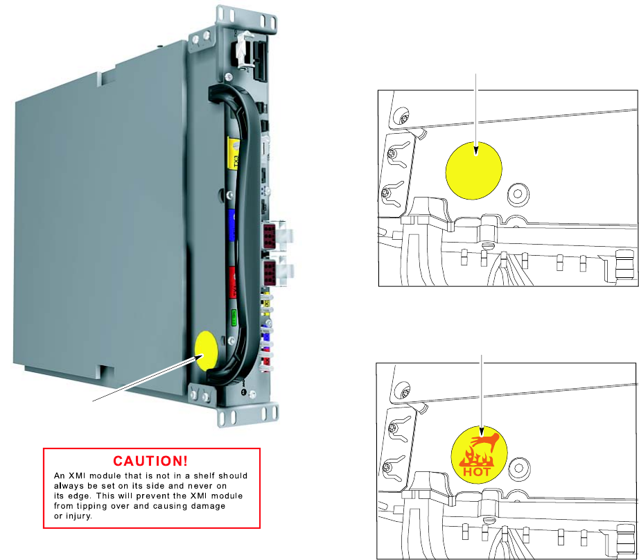
XMI (T r ansceiv er Module Internal) Module Chapter 7: XMI R eplacement Procedures
XMI “HOT" Warning Label Details
The XMI has a “HOT" warning label attached to it (see Figure 7 -1 for label location and
indications).
The hot warning label senses the surface temperature of the metal XMI housing. When the
XMI surface temperature reaches 50 degrees C , the “HOT" warning is fully visible indicating
that the XMI is too hot to touch and may cause burns. The “HOT" warning is partially visible
at temperatures that are slightly lower than 50 degrees C . When the “HOT" warning is not
visible at all, the XMI is safe to touch.
Figure 7 -1 XMI “HO T” W arning Label Details
ti-cdma-05889.eps
HOT
XMI Not Hot
Indication
XMI Hot Warning Label Close–ups
(XMI View Rotated 90 Degrees Clockwise)
XMI HOT
Indication
XMI
XMI Hot Warning Label Location
(See Label Close–ups)
CAUTION!
An XMI m o d u le th a t is n o t in a s h e lf s h o u ld
a lwa ys b e s e t o n its s id e a n d n e ve r o n
its e d g e . Th is will p re ve nt th e XMI m o d u le
fro m tip p in g o ve r a n d c a u s in g d a m a ge
o r in ju ry.
(Top-to-Bottom Positioning Shown Here
Is Same As When Installed In Frame)
7 -12 68P09283A64 -3
FOA SEP 2007

1X UBS Macro B T S FRU XMI (T r ansceiv er Module Internal) Module
Prerequisites
Do not touch the XMI with unprotected hands when the “HO T" label is fully visible. If
the “HO T" label is fully visible, wear heat protectiv e glo v es when touching the metal
case of the XMI. The “HO T" label becomes fully visible when the temper ature of the
metal case of the XMI reaches 50 degrees C. Howev er , the label ma y be partially
visible at lower case temper atures.
The XMI module is hea vy . T wo people are required to lift, carry , or handle the XMI
module.
•Be sure the remo v able XMI handle is attached to the front of the XMI before
ph ysically handling the module.
•Be sure two people use both hands and wear protectiv e footwear when handling
the XMI.
•Be sure to use two people to support the module while sliding the module out of
or into the shelf slot.
An XMI module that is not in a shelf should alw a ys be set on its side and nev er on
its edge. This will prev ent the XMI module from tipping o v er and causing damage
or injury .
This procedure requires working on or around circuitry extremely sensitiv e to ESD .
W ear a conductiv e, high impedance wrist str ap during the procedure.
F ollow appropriate safet y measures.
The XMI should be lock ed b y the OMCR oper ator just prior to being remo v ed.
68P09283A64 -3 7 -13
FOA SEP 2007

XMI (T r ansceiv er Module Internal) Module Chapter 7: XMI R eplacement Procedures
Coordinate this repair task with the OMCR operator .
Before You Begin
Before you begin, record the pertinent information in the following table (see T able 7 -3 ):
Table 7 -3 Item Number R eplacement List
Item
Number
BTS number
XMI number
XMI Replacement Procedures
The XMI replacement procedures consist of removing the failed XMI and then installing the
replacement XMI.
XMI Removal
F ollow the steps in Procedure 7 -1 to remove the XMI.
Procedure 7 -1 XMI R emo v al Procedure
A T THE BTS SITE
1
Notify the OMC-R operator that you are replacing the XMI.
A T THE OMCR
2
Open a CLI window . Refer to Accessing OMCR CLI window on page 3- 3 .
3
It will be helpful if the OMC-R operator executes “ENABLE EVENTS" command at the CLI
session of the OMC-R to monitor alarms. This command is optional and may not be useful if
executed during a high CP U utilization time.
4
Display the overall status of all devices at the BTS , including
the XMI, by entering the following command at the prompt:omc-00000> DISPLAY BTS-<bts#> STATUS
5
Determine the status of XMI 1 by observing the BTS ST A TUS report.
•F or a failed XMI 1 that is in an out-of -service (OOS) state, go to step 8 .
•F or a failed XMI 1 that is in an in service (INS) state, go to step 6 .
Continued
7 -14 68P09283A64 -3
FOA SEP 2007
1X UBS Macro B T S FRU XMI (T r ansceiv er Module Internal) Module
Procedure 7 -1 XMI R emo v al Procedure (Continued)
6
Lock the failed XMI by entering the following command at the prompt:omc-000000> LOCK XMI-<bts#>-<xmi#> UNC
7
Display the status of the XMI, by entering the following command at the prompt:omc-000000> DISPLAY BTS-<bts#> STATUS
V erify that the failed XMI is in an OOS_MANU AL state. Go to step 8 .
A T THE BTS SITE
8
Shut down DC power to the failed XMI by setting the corresponding XMI PDU DC circuit
breaker to OFF (pulled out).
Do not touch the XMI with unprotected hands when the “HO T" label is fully visible.
If the “HO T" label is fully visible, wear heat protectiv e glo v es when touching the
metal case of the XMI. The “HO T" label becomes fully visible when the temper ature
of the metal case of the XMI reaches 50 degrees C. Howev er , the label ma y be
partially visible at lower case temper atures.
W ear a conductiv e high impedance ESD wrist str ap while performing the steps
of this procedure.
9
F or cables, disconnect the cable b y pulling the connector - NOT b y pulling on the
cable.
If necessary , label the cables before disconnecting them to
ensure there is no uncertainty when reconnecting them.
Disconnect all cables from the XMI front panel and move them out of the
way .
10
F or 800 MHz XMI only , remove the TXD attenuator from the TXD connector on the XMI front
panel. This TXD attenuator will be reinstalled on the replacement XMI.
Continued
68P09283A64 -3 7 -15
FOA SEP 2007
XMI (T r ansceiv er Module Internal) Module Chapter 7: XMI R eplacement Procedures
Procedure 7 -1 XMI R emo v al Procedure (Continued)
11
A ttach the removable XMI handle to the front of the failed XMI module (see Figure 1-9
800 MHz XMI Module Front P anel I/O Detail on page 1- 38 or Figure 1-10 1.9 GHz XMI
Module Front P anel I/O Detail on page 1- 39 for location of XMI handle mounting screw
holes) as follows:
•Align handle screw holes with handle mounting screw holes on the XMI front panel.
(Note handle orientation; handle is not symmetrical.)
•Insert two M5 screws.
•Using a T25 TORX driver , tighten the screws to 3.2-3.6 N-m (28-32 in-lb).
12
Using a T25 TORX driver , remove the four XMI mounting screws; two screws at each of the
top and bottom mounting tabs on the front of the module.
13
The XMI module is hea vy . T wo people are required to lift, carry , or handle the
XMI module.
•Be sure the remo v able XMI handle is attached to the front of the XMI before
ph ysically handling the module.
•Be sure two people use both hands and wear protectiv e footwear when
handling the XMI.
•Be sure to use two people to support the module while sliding the module
out of or into the shelf slot.
An XMI module that is not in a shelf should alw a ys be set on its side and nev er on
its edge. This will prev ent the XMI module from tipping o v er and causing damage
or injury .
This step requires two people. P erform the following:
•(See Figure 7-2 T wo P eople Properly Removing/Installing an XMI (removable XMI handle
attached) on page 7- 17 .) One person grasp the XMI by the handle with both hands and
pull outward sliding the module out of the shelf slot. The second person supports the
bottom of the module with one hand and the top of the module with the other hand.
•(See Figure 7-3 T wo P eople Properly Carrying an XMI (removable XMI handle attached)
on page 7- 18 .) Carry the XMI module away from the frame and set it down on its side
not on its edge.
7 -16 68P09283A64 -3
FOA SEP 2007
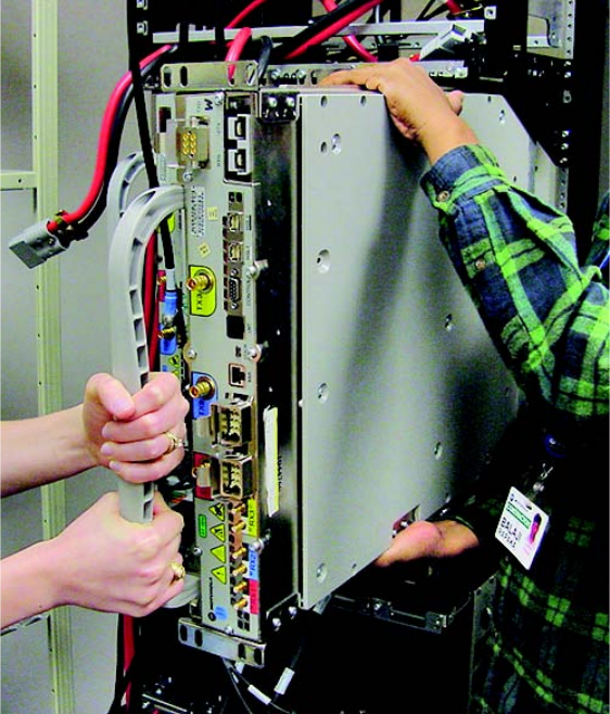
1X UBS Macro B T S FRU XMI (T r ansceiv er Module Internal) Module
Figure 7 -2 T wo P eople Properly R emo ving/Installing an XMI (remo v able XMI handle
attached)
ti-cdma-06375.eps
68P09283A64 -3 7 -17
FOA SEP 2007