Novatel Wireless NRM-EU860D Dual Band Licensed Modular Transmitter User Manual Part 1
Novatel Wireless, Inc. Dual Band Licensed Modular Transmitter Part 1
Contents
- 1. Part 1
- 2. Part 2
- 3. Manual 1
- 4. Manual 2
- 5. Manual 3
- 6. Manual 4
- 7. User Manual 1
- 8. User Manual 2
- 9. User Manual M1210
- 10. User Manual D430
- 11. User Manual D420
- 12. User Manual Corsica
- 13. User Manual Sapporo
- 14. User Manual Vostro 1
- 15. User Manual Vostro 2
- 16. Users Manual Vostro 3
- 17. Users Manual Vostro 4
- 18. User Manual 3
- 19. User Manual 4
- 20. User Manual Gilligan
Part 1
![Proprietary & Confidential 8 Novatel Wireless Doc No. OM-01017857 Rev 1 Reference Documents PCI Express Mini Card References PCI Express Mini Card Electromehcanical Specification Revision 1.0 June 2, 2003 PCI Express Card Electromechancil Specification revision 1.1 March 28th 2005 SMBus Specification, Revision 2.0 The I2C-BUS SPECIFICATION Version 2.1 January 2000 3GPP References The following documents contain provisions which, through reference in this text, constitute provisions of the present document. References are either specific (identified by date of publication, edition number, version number, etc.) or non-specific. For a specific reference, subsequent revisions do not apply. For a non-specific reference, the latest version applies. In the case of a reference to a 3GPP document (including a GSM document), a non-specific reference implicitly refers to the latest version of that document in the same Release as the present document. [1] Void. [2] 3GPP TS 23.038: "Alphabets and language-specific information". [3] 3GPP TS 23.040: "Technical realization of the Short Message Service (SMS) ". [4] 3GPP TS 23.041: "Technical realization of the Cell Broadcast Service (CBS)". [5] 3GPP TS 24.008: "Mobile Radio Interface Layer 3 specification; Core Network Protocols; Stage 3". [6] 3GPP TS 24.011: "Short Message Service (SMS) support on mobile radio interface". [7] 3GPP TS 24.012: "Cell Broadcast Service (CBS) support on the mobile radio interface". [8] 3GPP TS 27.001: "General on Terminal Adaptation Functions (TAF) for Mobile Stations (MS)". [9] 3GPP TS 27.007: "AT command set for User Equipment (UE)". [10] 3GPP TS 51.011: "Specification of the Subscriber Identity Module - Mobile Equipment (SIM - ME) interface". [11] ITU-T Recommendation V.25ter: "Serial asynchronous automatic dialing and control". [12] ITU-T Recommendation V.24: "List of definitions for interchange circuits between data terminal equipment (DTE) and data circuit-terminating equipment (DCE)". [13] ITU-T Recommendation E.164: "The international public telecommunication numbering plan".](https://usermanual.wiki/Novatel-Wireless/NRM-EU860D.Part-1/User-Guide-754578-Page-8.png)
![Proprietary & Confidential 9 Novatel Wireless Doc No. OM-01017857 Rev 1 [14] ITU-T Recommendation E.163: "Numbering plan for the international telephone service". [15] 3GPP TR 21.905: "Vocabulary for 3GPP Specifications". [16] 3GPP TS 31.102: "Characteristics of the USIM application.](https://usermanual.wiki/Novatel-Wireless/NRM-EU860D.Part-1/User-Guide-754578-Page-9.png)
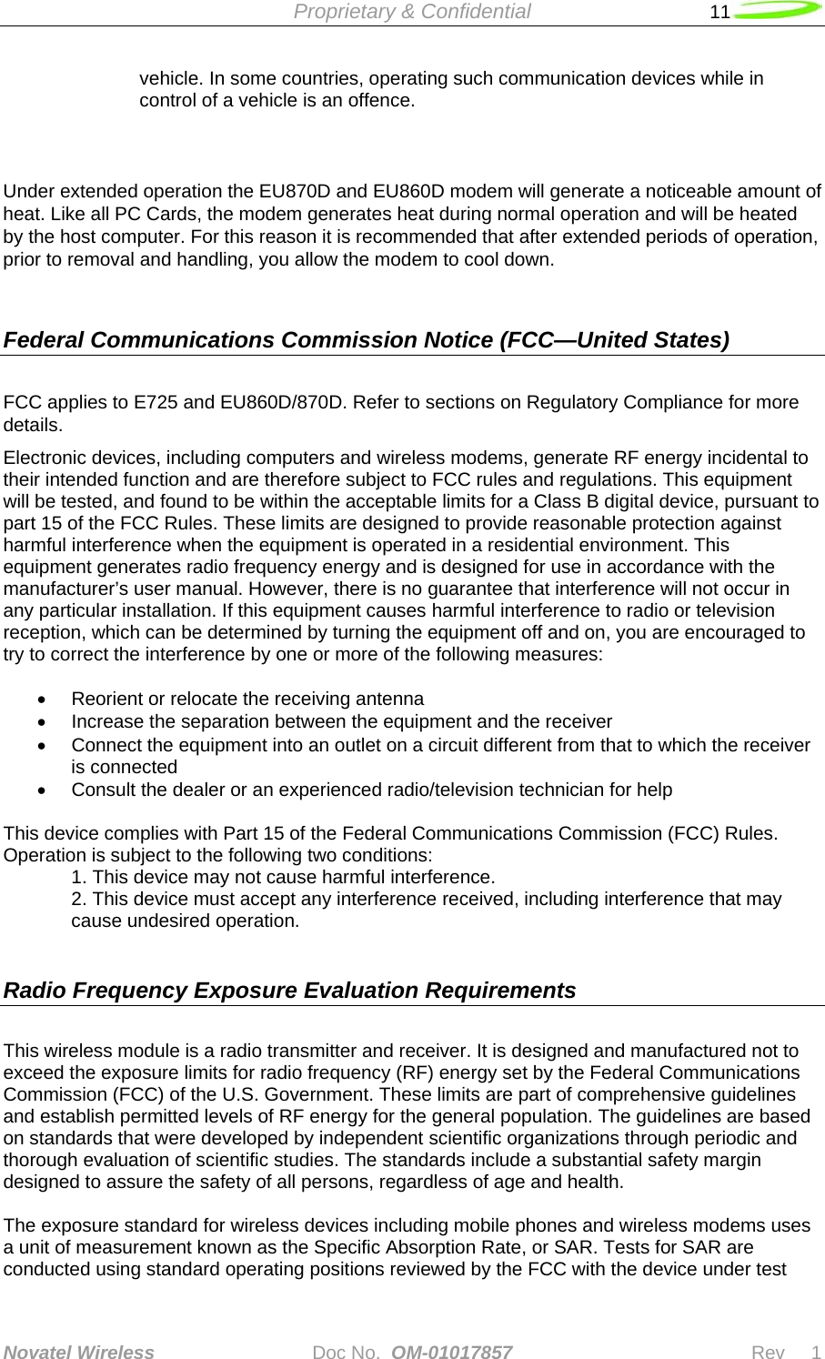
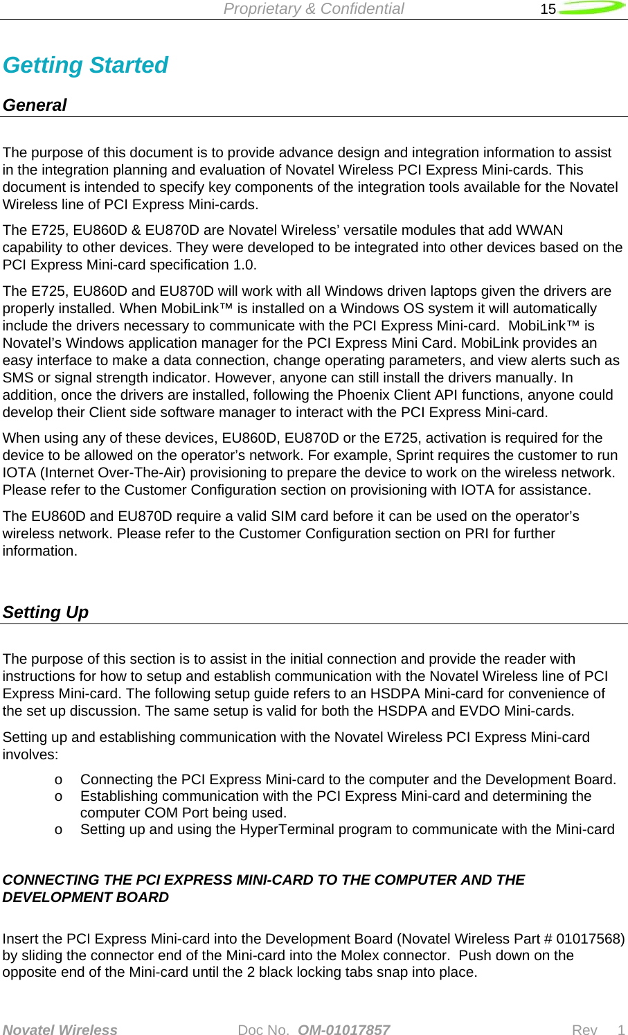
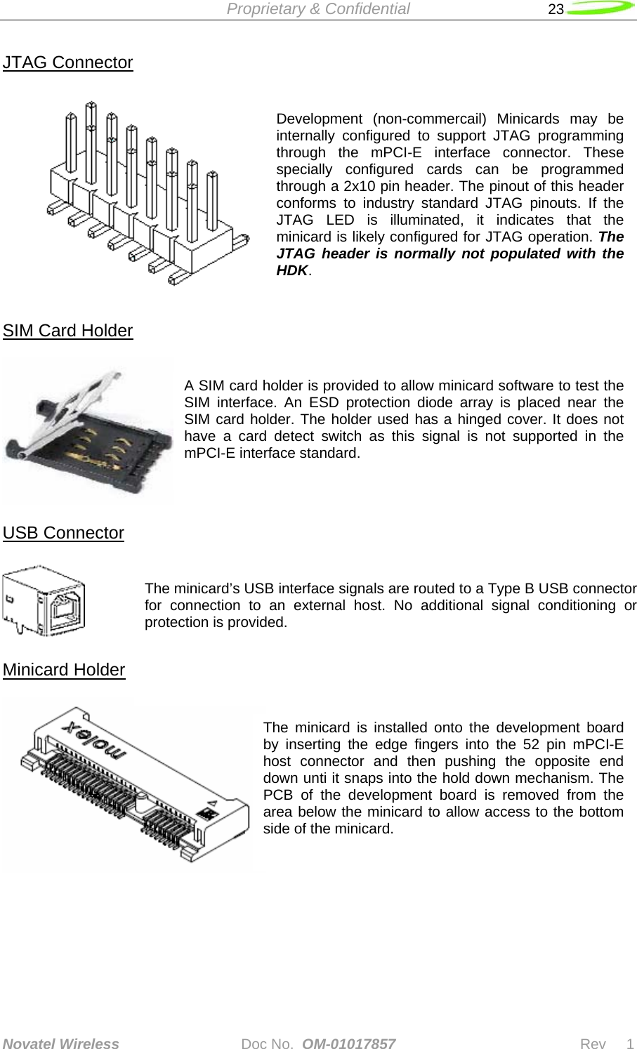
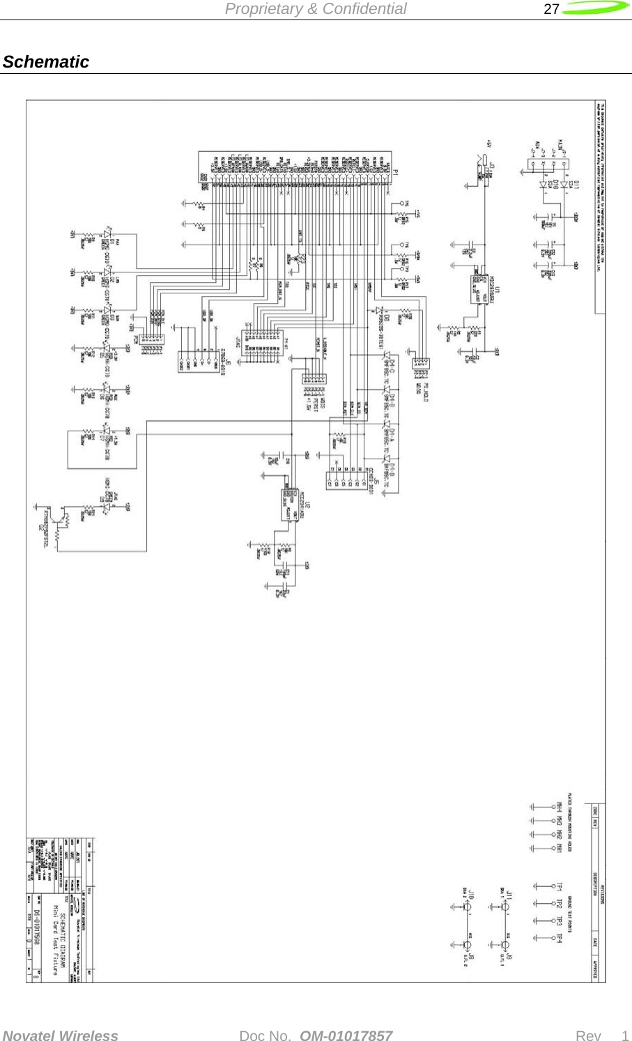
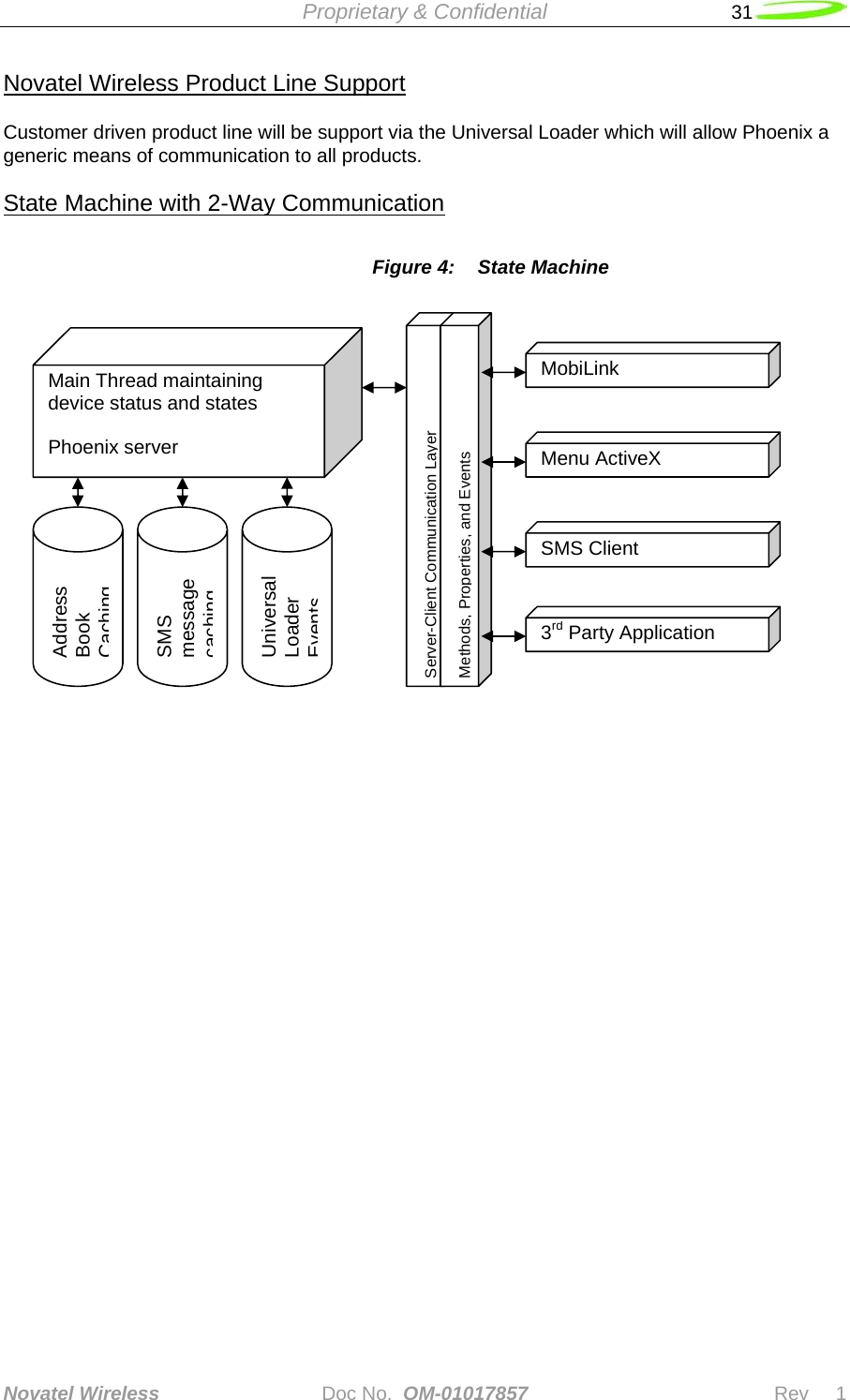
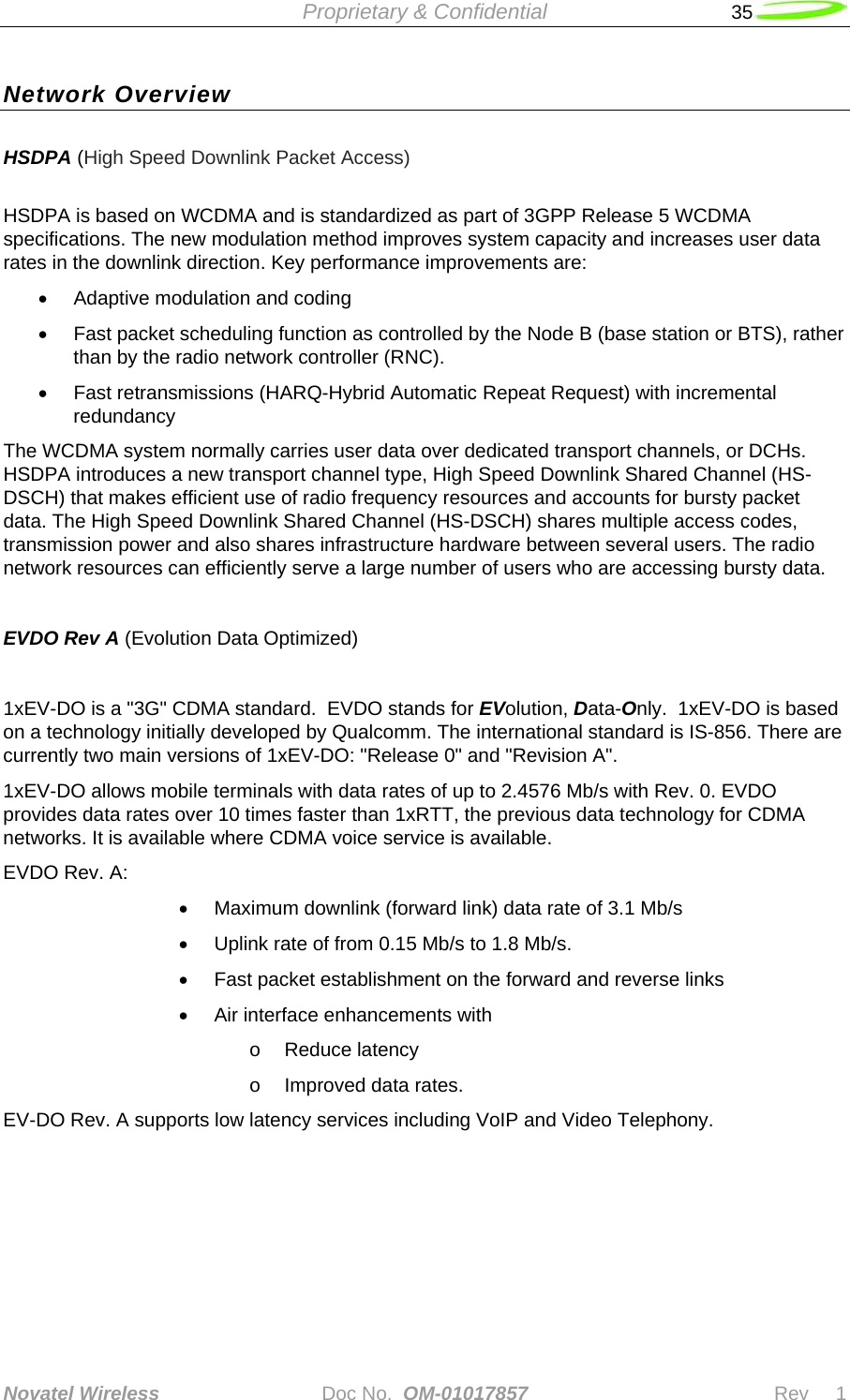
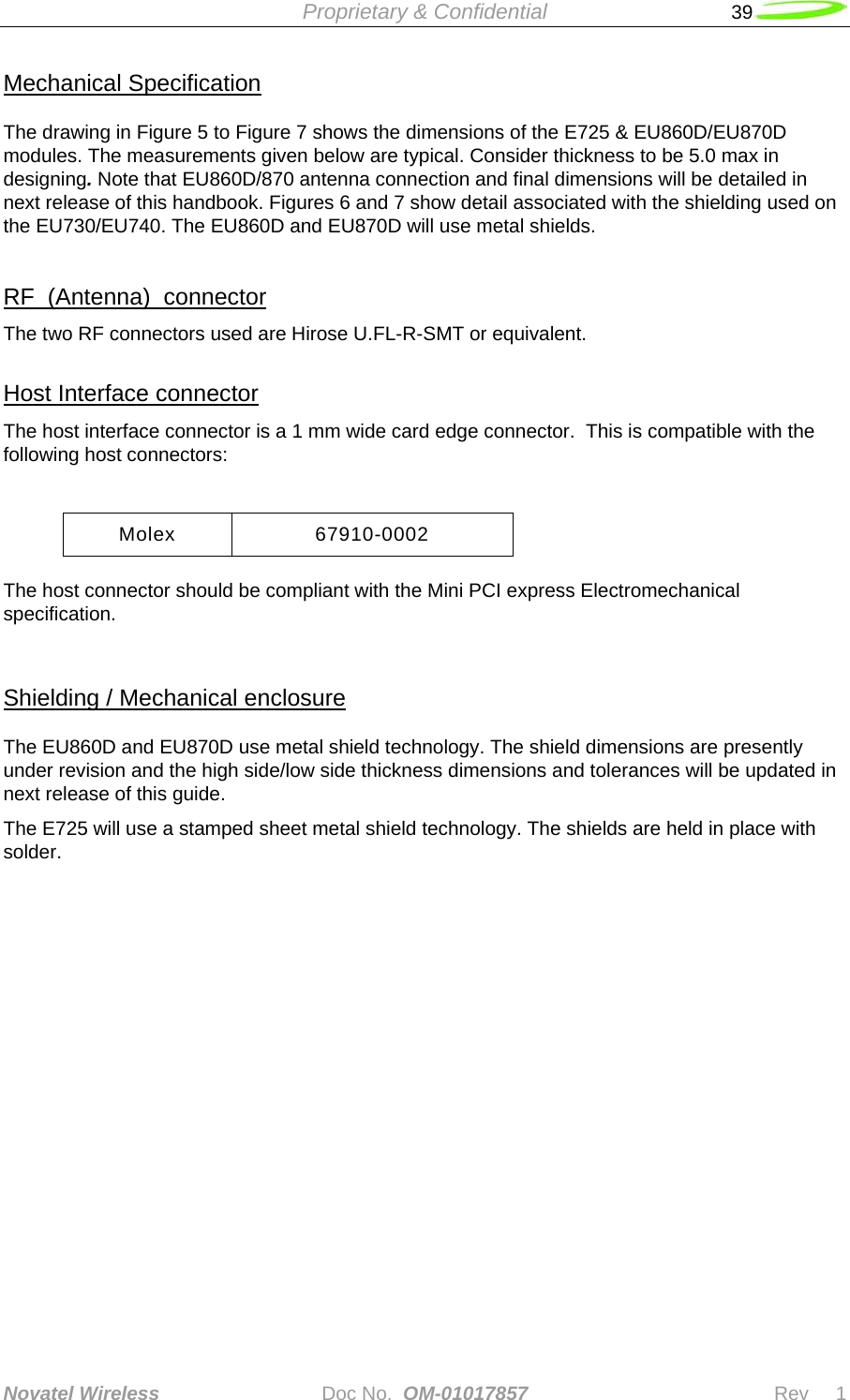
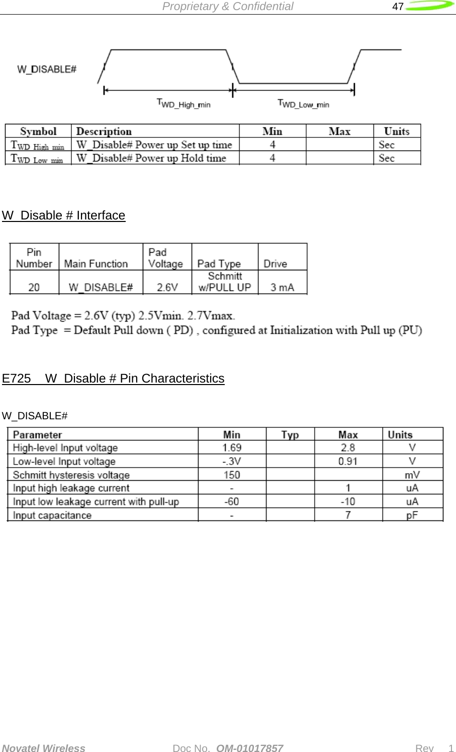
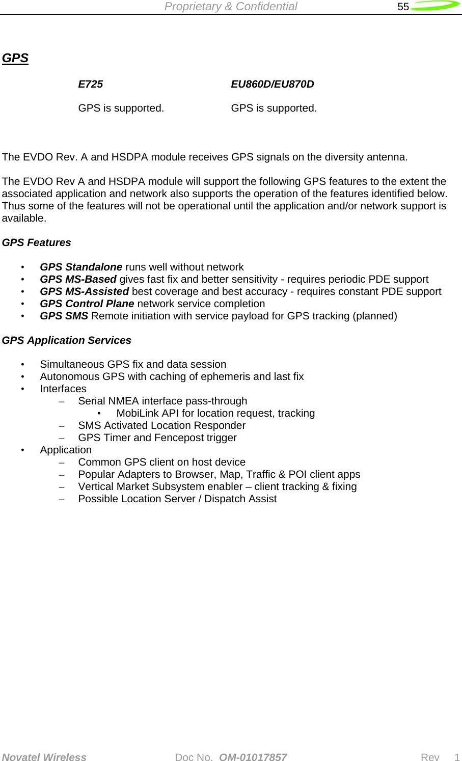
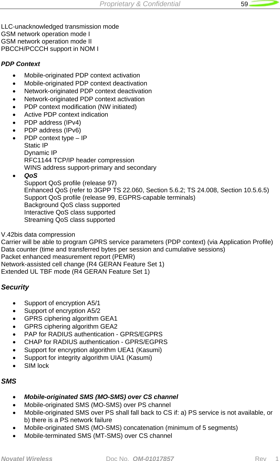
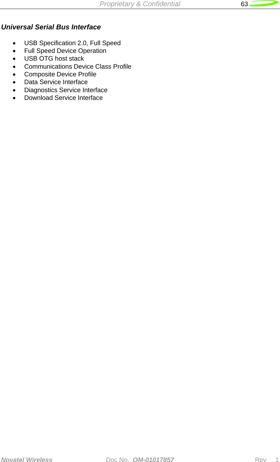
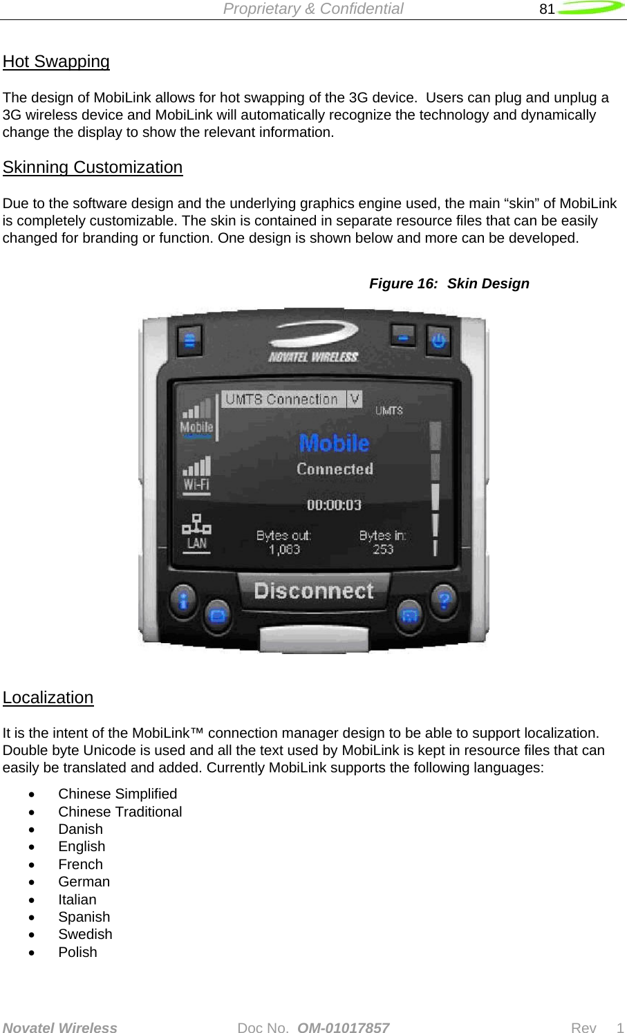
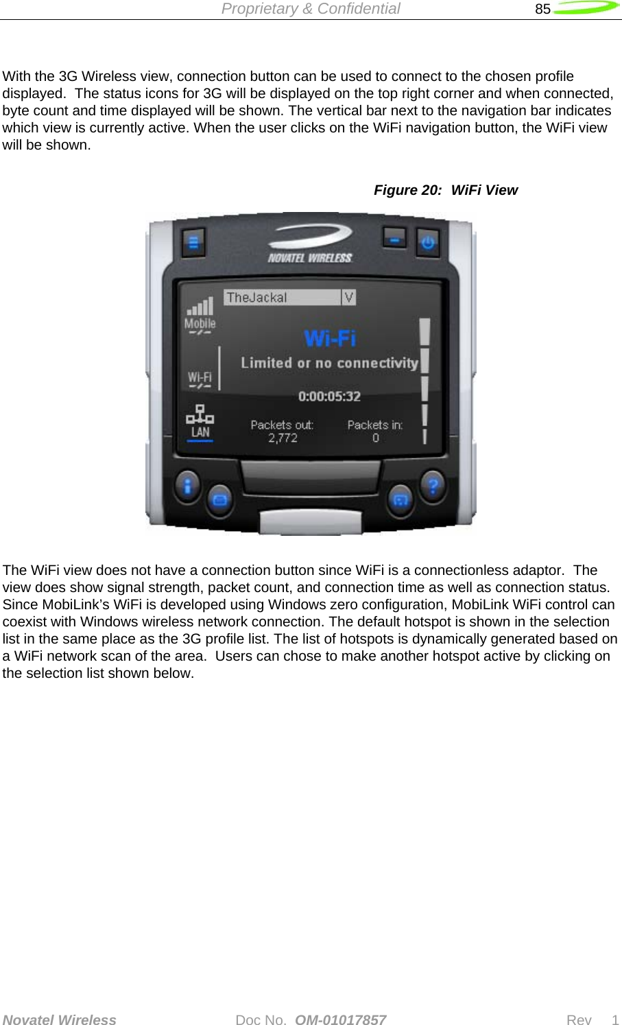
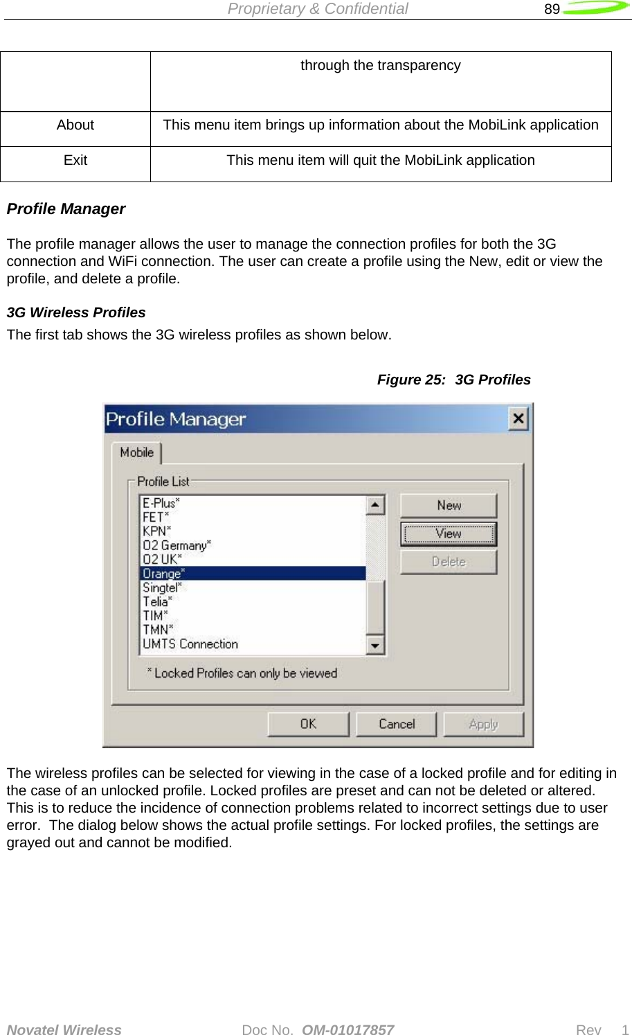
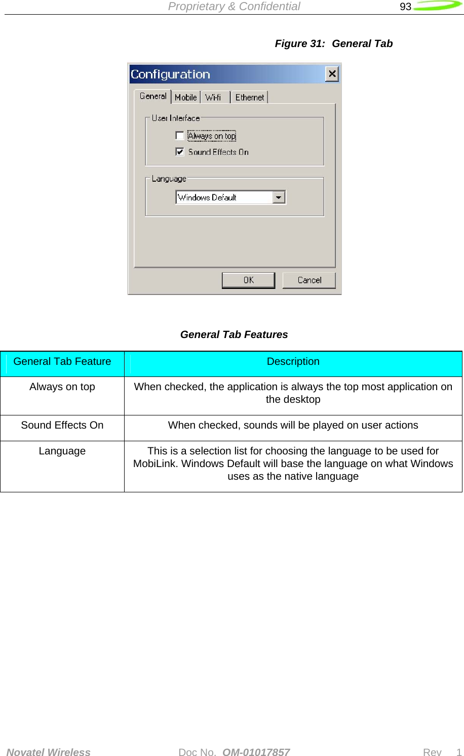
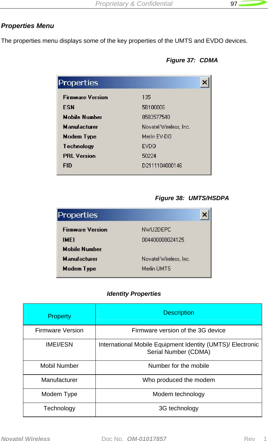
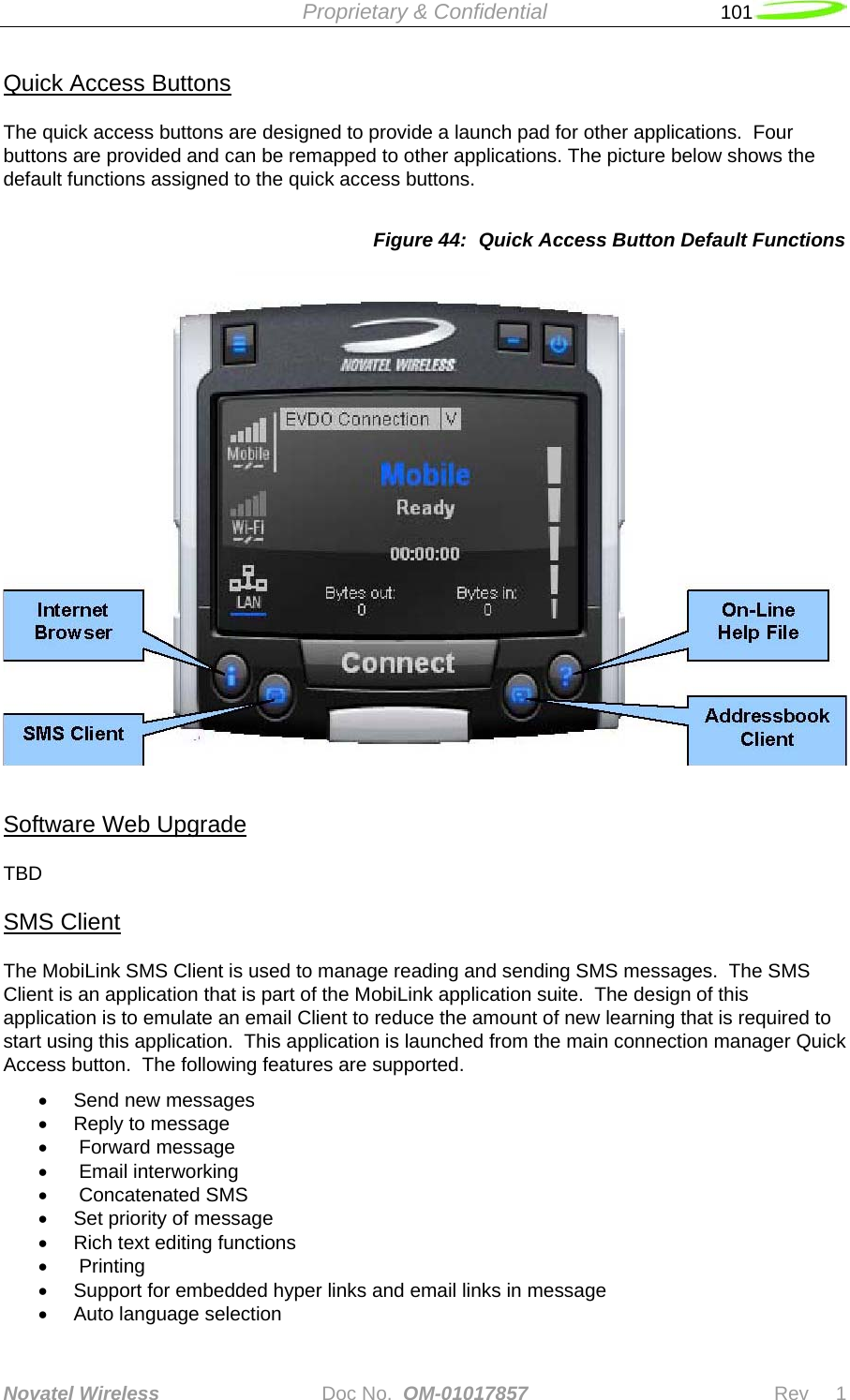
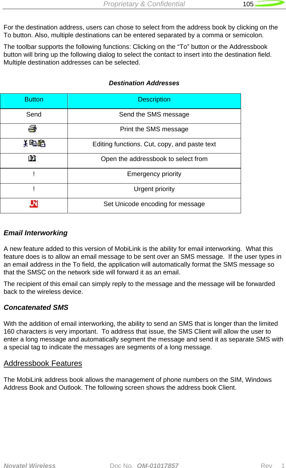
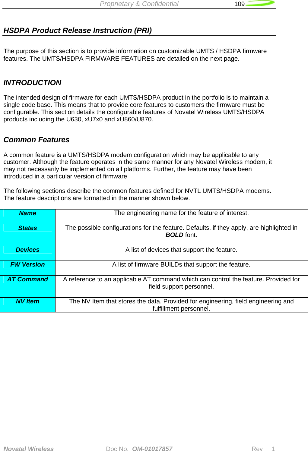
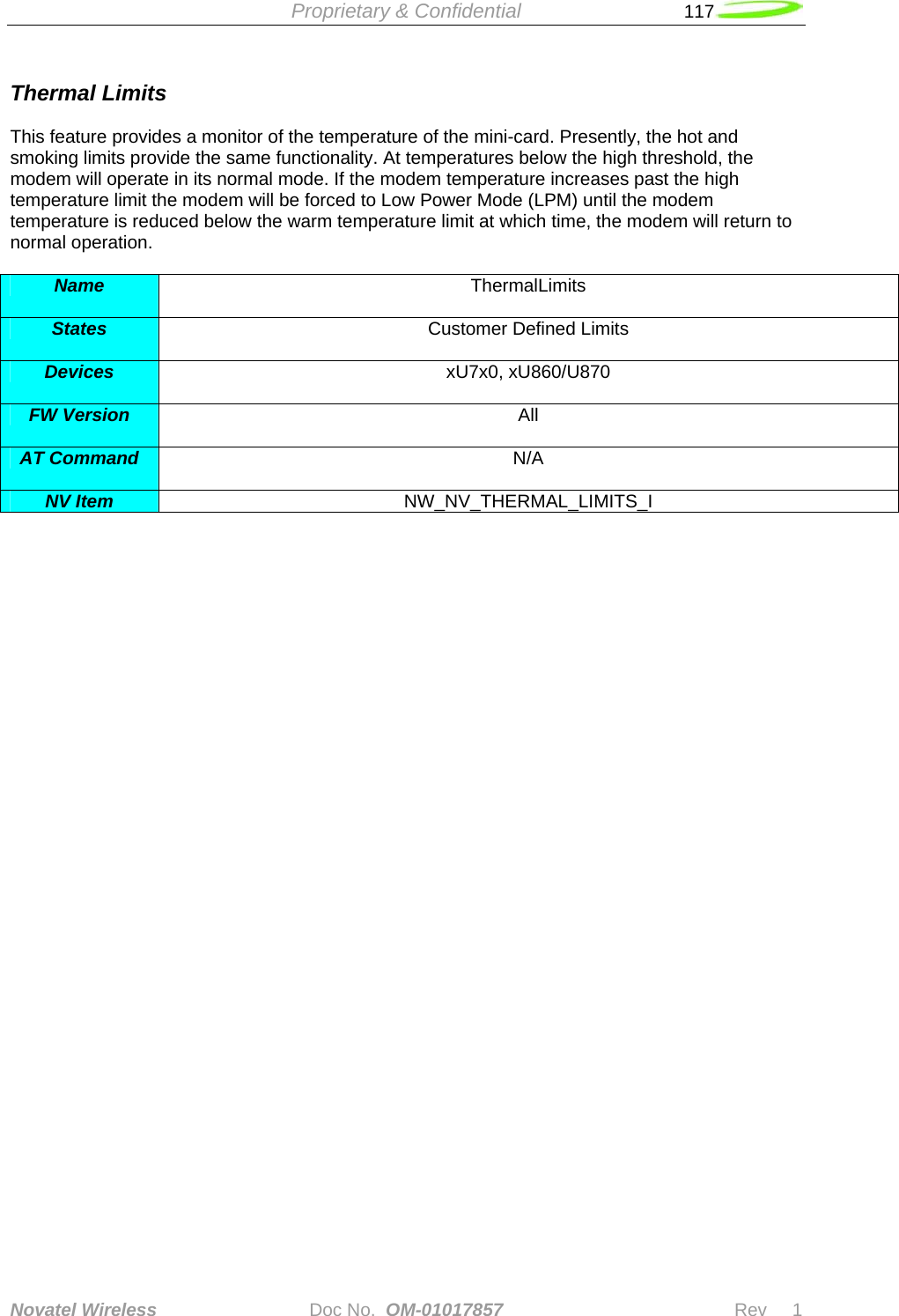
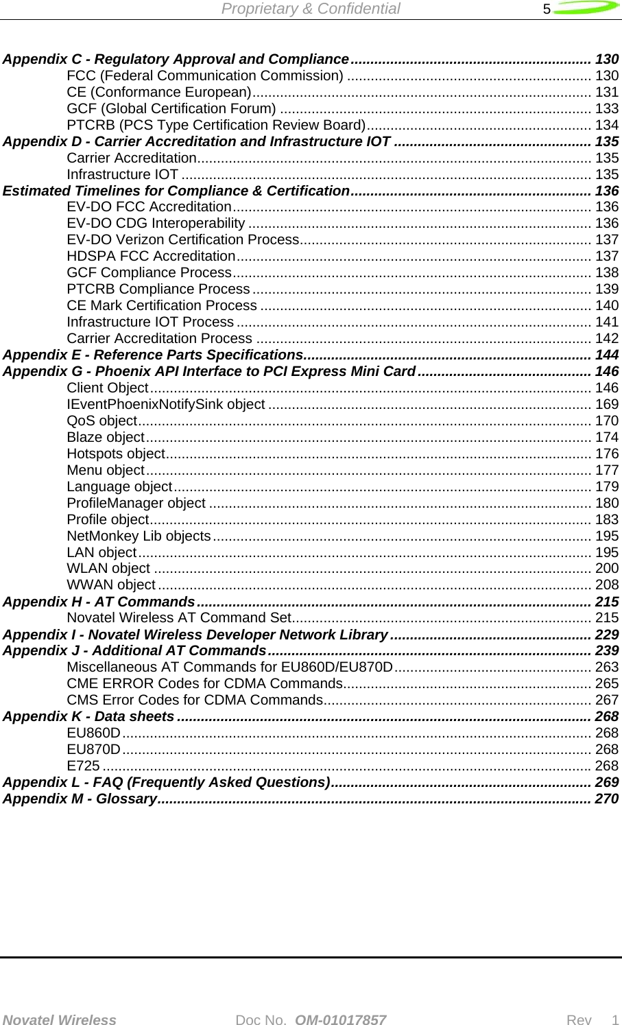
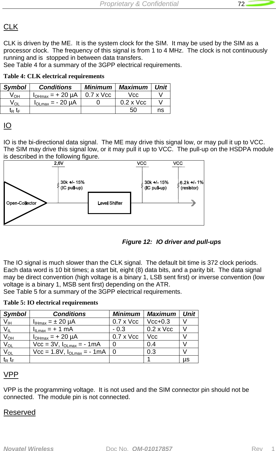
![Proprietary & Confidential 70 Novatel Wireless Doc No. OM-01017857 Rev 1 SIM Design Guidelines Description The SIM contains subscriber identification, specification and authentication information; and is required to obtain service. 3.0V and 1.8V SIMs are supported. The physical size and contact location for the “Plug-in SIM” format is defined in reference [2]. Contact identification is defined in reference [7]. Electrical characteristics for a 3V SIM are defined in reference [3], and for a 1.8V SIM in reference [4]. Power sequencing and general protocol operation is defined in reference [8]. The figure below shows a “Plug-in SIM”. C1VCC C5GNDC2RST C6VPPC3CLK C7IOC4reserved C8reserved Figure 11: Plug-in SIM (shown from contact side) References 1. 3GPP TS 01.04: "Abbreviations and acronyms" 2. 3GPP TS 11.11: “Specification of the Subscriber Identity Module - Mobile Equipment (SIM - ME) interface” 3. 3GPP TS 11.12: "Specification of the 3 Volt Subscriber Identity Module - Mobile Equipment (SIM - ME) interface". 4. 3GPP TS 11.18: “Specification of the 1.8 Volt Subscriber Identity Module - Mobile Equipment (SIM - ME) interface” 5. 3GPP TS 51.010-1 “Mobile Station (MS) conformance specification; Part 1: Conformance specification” 6. ISO/IEC 7816-1: “Identification cards – Integrated circuit cards with contacts – Part 1: Physical characteristics” 7. ISO/IEC 7816-2: “Identification cards – Integrated circuit cards with contacts – Part 2: Dimensions and locations of the contacts 8. ISO/IEC 7816-3 “Identification cards – Integrated circuit cards with contacts – Part 3: Electronic signals and transmission protocols” Operation of SIM interface For the purposes of this document, the SIM interface is the interface between the SIM and the laptop at the SIM connector. The ME includes the HSDPA module and laptop SIM circuit. The SIM interface provides power, clock, reset and data to the SIM. The data is half-duplex (bi-directional but only able to transfer data in one direction at any time) circuit implemented as an open-collector signal. When data is transmitted, the ME or the SIM will pull the line to a low voltage, otherwise the line is pulled up through a resistor. The SIM operates in a command/response mode where it will only transmit data in response to a received command. One exception to this is the Answer-To-Reset (ATR) when the SIM transmits data in response to a reset.](https://usermanual.wiki/Novatel-Wireless/NRM-EU860D.Part-1/User-Guide-754578-Page-70.png)
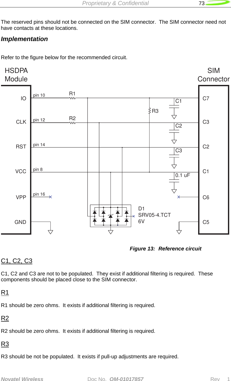
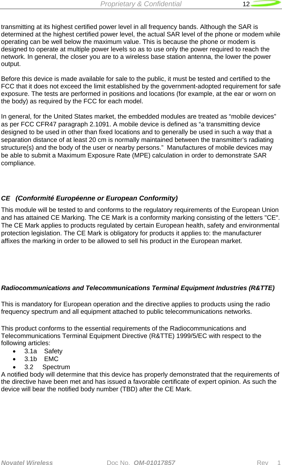
![Proprietary & Confidential 74 Novatel Wireless Doc No. OM-01017857 Rev 1 D1 D1 should be a low capacitance ESD diode array (5 pF or less). It is important to minimize the capacitance on the IO line. D1 should be placed close to the SIM connector. There is no ESD protection on the HSDPA module. It is recommended that the ESD protection meet IEC61000-4-2, level 4 (±15kV air, ±8kV contact). Signal routing The CLK line is a high speed digital signal and care must be taken to insure it is isolated from the other signals. A guard trace between it and the other signals should be used if they are to be adjacent for any length. A multi-layer PCB with a ground plane should be used. Traces should be as short as possible. All the SIM interface signals should be routed carefully to avoid being corrupted by each other or external signals. IO signal capacitance The rise time of the IO signal is determined by the total capacitance on the line and the pull-up resistance. The module has a maximum capacitance of 50 pF and the SIM is considered to have a maximum capacitance of 30 pF. The laptop capacitance on the IO signal (including connectors) should be as targeted to be lower than 30 pF. Additional capacitance may be required to reduce noise, however the IO circuit rise time limit of 1 µs must be considered. IO signal resistance The SIM may also have a pull-up on the IO signal, which would have the effect of injecting up to 1 mA into the ME when the ME is transmitting a low level. Series resistance of the IO signal must be kept very low as the voltage drop across it due to the injected current may cause the output voltage to rise above the voltage output low specification. Certification As the SIM interface is unique to each laptop, each laptop must pass several test cases to obtain certification. The SIM electrical test cases are specified in section 27.17.2 in reference [5]. The following is a summary of these tests: • 27.17.2.1.1 Electrical tests on contact C1 (VCC) – Test 1 e.1) The voltage on contact C1 of the SIM/ME interface shall be 3V ± 10 % for Icc up to 6 mA when the interface is in 3V operation mode. e.2) The voltage on contact C1 of the SIM/ME interface shall be 1.8V ± 10 % for Icc up to 4 mA when the interface is in 1.8V operation mode. • 27.17.2.1.2 Electrical tests on contact C1 (VCC) – Test 2 e.1) The voltage on contact C1 of the SIM/ME interface shall be 3V ± 10 % for spikes in the current consumption with a maximum charge of 12 nAs with no more than 400 ns duration and an amplitude of at most 60 mA when the interface is in 3V operation mode. e.2) The voltage on contact C1 of the SIM/ME interface shall be 1.8V ± 10 % for spikes in the current consumption with a maximum charge of 12 nAs with no more than 400 ns duration and an amplitude of at most 60 mA when the interface is in 1.8V operation mode.](https://usermanual.wiki/Novatel-Wireless/NRM-EU860D.Part-1/User-Guide-754578-Page-74.png)